1
R
Reference Designs
System Monitor
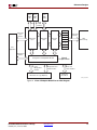
Every member of the Virtex-5 FPGA family contains a single System Monitor (Figure 6),
which is located in the center of every die. The System Monitor function is built around a
10-bit, 200-kSPS (kilosamples per second) Analog-to-Digital Converter (ADC). When
combined with a number of on-chip sensors, the ADC is used to measure FPGA physical
operating parameters like on-chip power supply voltages and die temperatures. Access to
external voltages is provided through a dedicated analog-input pair (VP/VN) and 16 userselectable analog inputs, known as auxiliary analog inputs (VAUXP[15:0], VAUXN[15:0]).
The external analog inputs allow the ADC to monitor the physical environment of the
board or enclosure. System Monitor is fully functional on power up, and measurement
data can be accessed via the JTAG port pre-configuration.
System Monitor
VAUXP[0]
VAUXN[0]
VAUXP[14]
VAUXN[14]
Mux
VAUXP[15]
VAUXN[15]
VP
VN
Temperature
Sensor
Mux
°C
10-Bits
200 kSPS
ADC
Register File Interface
00h
01h
02h
03h
40h
41h
42h
43h
Status Registers
Control Registers
3Eh
3Fh
7Eh
7Fh
Control Logic
Dynamic
Reconfiguration
Port (DRP)
VCCINT
VCCAUX
VREFP
VREFN
Supply Sensor
Internal Supplies
STATUS ALARM
CLOCK
and
CONTROL
DRP
FPGA Interconnect
JTAG TAP
Controller
UG349_06_062309
Figure 6:
System Monitor Block Diagram
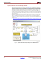
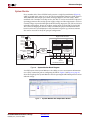
A useful feature of the System Monitor is the ability to access measurement information
over a JTAG connection prior to configuring the FPGA. Figure 7 and Figure 8, page 22
show the ChipScope Pro System Monitor console reporting the ML510 temperature and an
onboard voltage.
Figure 7:
ML505/ML506/ML507 Reference Design
UG349 (v3.1) June 23, 2009
System Monitor Die Temperature Sensor
www.xilinx.com
21