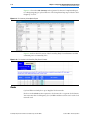
1
PowerPlay Early Power Estimator User Guide for Cyclone III FPGAs 101 Innovation Drive San Jose, CA 95134 www.altera.com UG-01013-2.0 Software Version: Document Version: Document Date: QII v9.0 SP2 2.0 June 2009 Copyright © 2009 Altera Corporation. All rights reserved. Altera, The Programmable Solutions Company, the stylized Altera logo, specific device designations, and all other words and logos that are identified as trademarks and/or service marks are, unless noted otherwise, the trademarks and service marks of Altera Corporation in the U.S. and other countries. All other product or service names are the property of their respective holders. Altera products are protected under numerous U.S. and foreign patents and pending applications, maskwork rights, and copyrights. Altera warrants performance of its semiconductor products to current specifications in accordance with Altera's standard warranty, but reserves the right to make changes to any products and services at any time without notice. Altera assumes no responsibility or liability arising out of the application or use of any information, product, or service described herein except as expressly agreed to in writing by Altera Corporation. Altera customers are advised to obtain the latest version of device specifications before relying on any published information and before placing orders for products or services. UG-01013-2.0 Contents Chapter 1. About Cyclone III PowerPlay Early Power Estimator Release Information . . . . . . . . . . . . . . . . . . . . . . . . . . . . . . . . . . . . . . . . . . . . . . . . . . . . . . . . . . . . . . . . . . . . . 1–1 Device Family Support . . . . . . . . . . . . . . . . . . . . . . . . . . . . . . . . . . . . . . . . . . . . . . . . . . . . . . . . . . . . . . . . . . . 1–1 General Description . . . . . . . . . . . . . . . . . . . . . . . . . . . . . . . . . . . . . . . . . . . . . . . . . . . . . . . . . . . . . . . . . . . . . 1–1 Features . . . . . . . . . . . . . . . . . . . . . . . . . . . . . . . . . . . . . . . . . . . . . . . . . . . . . . . . . . . . . . . . . . . . . . . . . . . . . . . . 1–2 Chapter 2. Setting Up Cyclone III PowerPlay Early Power Estimator System Requirements . . . . . . . . . . . . . . . . . . . . . . . . . . . . . . . . . . . . . . . . . . . . . . . . . . . . . . . . . . . . . . . . . . . . 2–1 Download and Install PowerPlay Early Power Estimator . . . . . . . . . . . . . . . . . . . . . . . . . . . . . . . . . . . . . 2–1 Estimating Power . . . . . . . . . . . . . . . . . . . . . . . . . . . . . . . . . . . . . . . . . . . . . . . . . . . . . . . . . . . . . . . . . . . . . . . 2–1 Estimating Power Before Creating FPGA Design . . . . . . . . . . . . . . . . . . . . . . . . . . . . . . . . . . . . . . . . . . 2–2 Estimating Power While Creating the FPGA Design . . . . . . . . . . . . . . . . . . . . . . . . . . . . . . . . . . . . . . . 2–2 Estimating Power After Completing the FPGA Design . . . . . . . . . . . . . . . . . . . . . . . . . . . . . . . . . . . . . 2–3 Entering Information into the PowerPlay Early Power Estimator . . . . . . . . . . . . . . . . . . . . . . . . . . . . . . 2–4 Clearing All Values . . . . . . . . . . . . . . . . . . . . . . . . . . . . . . . . . . . . . . . . . . . . . . . . . . . . . . . . . . . . . . . . . . . 2–4 Manually Entering Information . . . . . . . . . . . . . . . . . . . . . . . . . . . . . . . . . . . . . . . . . . . . . . . . . . . . . . . . . 2–4 Importing a File . . . . . . . . . . . . . . . . . . . . . . . . . . . . . . . . . . . . . . . . . . . . . . . . . . . . . . . . . . . . . . . . . . . . . . . 2–4 Chapter 3. Using Cyclone III PowerPlay Early Power Estimator Introduction . . . . . . . . . . . . . . . . . . . . . . . . . . . . . . . . . . . . . . . . . . . . . . . . . . . . . . . . . . . . . . . . . . . . . . . . . . . . 3–1 PowerPlay Early Power Estimator Inputs . . . . . . . . . . . . . . . . . . . . . . . . . . . . . . . . . . . . . . . . . . . . . . . . . . . 3–1 Main Input Parameters . . . . . . . . . . . . . . . . . . . . . . . . . . . . . . . . . . . . . . . . . . . . . . . . . . . . . . . . . . . . . . . . 3–1 Logic . . . . . . . . . . . . . . . . . . . . . . . . . . . . . . . . . . . . . . . . . . . . . . . . . . . . . . . . . . . . . . . . . . . . . . . . . . . . . . . . 3–4 RAM Blocks . . . . . . . . . . . . . . . . . . . . . . . . . . . . . . . . . . . . . . . . . . . . . . . . . . . . . . . . . . . . . . . . . . . . . . . . . . 3–6 DSP . . . . . . . . . . . . . . . . . . . . . . . . . . . . . . . . . . . . . . . . . . . . . . . . . . . . . . . . . . . . . . . . . . . . . . . . . . . . . . . . . 3–9 General I/O Pins . . . . . . . . . . . . . . . . . . . . . . . . . . . . . . . . . . . . . . . . . . . . . . . . . . . . . . . . . . . . . . . . . . . . . 3–11 Phase-Locked Loops . . . . . . . . . . . . . . . . . . . . . . . . . . . . . . . . . . . . . . . . . . . . . . . . . . . . . . . . . . . . . . . . . 3–15 Clocks . . . . . . . . . . . . . . . . . . . . . . . . . . . . . . . . . . . . . . . . . . . . . . . . . . . . . . . . . . . . . . . . . . . . . . . . . . . . . . 3–16 Power Analysis . . . . . . . . . . . . . . . . . . . . . . . . . . . . . . . . . . . . . . . . . . . . . . . . . . . . . . . . . . . . . . . . . . . . . . . . 3–18 Thermal Power . . . . . . . . . . . . . . . . . . . . . . . . . . . . . . . . . . . . . . . . . . . . . . . . . . . . . . . . . . . . . . . . . . . . . . 3–18 Thermal Analysis . . . . . . . . . . . . . . . . . . . . . . . . . . . . . . . . . . . . . . . . . . . . . . . . . . . . . . . . . . . . . . . . . . . . 3–19 Not Using a Heat Sink . . . . . . . . . . . . . . . . . . . . . . . . . . . . . . . . . . . . . . . . . . . . . . . . . . . . . . . . . . . . . . 3–20 Using a Heat Sink . . . . . . . . . . . . . . . . . . . . . . . . . . . . . . . . . . . . . . . . . . . . . . . . . . . . . . . . . . . . . . . . . 3–21 Power Supply Current (A) . . . . . . . . . . . . . . . . . . . . . . . . . . . . . . . . . . . . . . . . . . . . . . . . . . . . . . . . . . . . 3–23 Factors Affecting PowerPlay Early Power Estimator Accuracy . . . . . . . . . . . . . . . . . . . . . . . . . . . . . . . . 3–24 Toggle Rate . . . . . . . . . . . . . . . . . . . . . . . . . . . . . . . . . . . . . . . . . . . . . . . . . . . . . . . . . . . . . . . . . . . . . . . . . 3–24 Airflow . . . . . . . . . . . . . . . . . . . . . . . . . . . . . . . . . . . . . . . . . . . . . . . . . . . . . . . . . . . . . . . . . . . . . . . . . . . . . 3–26 Temperature . . . . . . . . . . . . . . . . . . . . . . . . . . . . . . . . . . . . . . . . . . . . . . . . . . . . . . . . . . . . . . . . . . . . . . . . 3–27 Heat Sink . . . . . . . . . . . . . . . . . . . . . . . . . . . . . . . . . . . . . . . . . . . . . . . . . . . . . . . . . . . . . . . . . . . . . . . . . . . 3–28 Additional Information Revision History . . . . . . . . . . . . . . . . . . . . . . . . . . . . . . . . . . . . . . . . . . . . . . . . . . . . . . . . . . . . . . . . . . . . . Info–1 How to Contact Altera . . . . . . . . . . . . . . . . . . . . . . . . . . . . . . . . . . . . . . . . . . . . . . . . . . . . . . . . . . . . . . . . Info–1 Typographic Conventions . . . . . . . . . . . . . . . . . . . . . . . . . . . . . . . . . . . . . . . . . . . . . . . . . . . . . . . . . . . . . Info–1 © June 2009 Altera Corporation PowerPlay Early Power Estimator User Guide for Cyclone III FPGAs iv PowerPlay Early Power Estimator User Guide for Cyclone III FPGAs © June 2009 Altera Corporation 1. About Cyclone III PowerPlay Early Power Estimator Release Information This user guide explains how to use the Cyclone® III PowerPlay Early Power Estimator spreadsheet version 9.0 SP2 and later to estimate device power consumption. Device Family Support The Microsoft Excel-based PowerPlay Early Power Estimator spreadsheet provides preliminary support for the Cyclone III device family. General Description As designs grow larger and processes continue to shrink, power concerns increase. PCB designers need an accurate estimate of power the device consumes to develop an appropriate power budget and design the power supplies, voltage regulators, heat sink, and cooling system. You can calculate the power requirements of a Cyclone III device family by using the Microsoft Excel-based PowerPlay Early Power Estimator from the PowerPlay Early Power Estimators (EPE) and Power Analyzer page on the Altera website, or the PowerPlay Power Analyzer in the Quartus® II. To access the PowerPlay Power Analyzer in the Quartus II software, open Quartus II, point to Processing, and choose the PowerPlay Power Analyzer Tool option. You must enter the device resources, operating frequency, toggle rates, and other parameters in the PowerPlay Early Power Estimator. 1 f © June 2009 These calculations are only meant to be used as an estimate of power, and not as a specification. You must ensure that you verify the actual power during device operation, as the information is sensitive to the device design and the environmental operating conditions. For more information about available device resources, I/O standard support, and other device features, refer to the appropriate device family handbooks. Altera Corporation PowerPlay Early Power Estimator User Guide for Cyclone III FPGAs 1–2 Chapter 1: About Cyclone III PowerPlay Early Power Estimator Features Features With the PowerPlay Early Power Estimator you are able to: ■ Estimate your design's power usage before creating the design, during the design process, or after the design is complete. ■ Import device resource information from the Quartus II software into the PowerPlay Early Power Estimator with the use of the Quartus II-generated PowerPlay Early Power Estimator file. ■ Perform preliminary thermal analysis of your design. PowerPlay Early Power Estimator User Guide for Cyclone III FPGAs © June 2009 Altera Corporation 2. Setting Up Cyclone III PowerPlay Early Power Estimator System Requirements The PowerPlay Early Power Estimator requires: ■ A personal computer (PC) with Windows NT, 2000, or XP operating system ■ Microsoft Excel 2003 or later ■ Quartus® II software version 9.0 SP2 or later (if generating a file for import) Download and Install PowerPlay Early Power Estimator The Cyclone® III PowerPlay Early Power Estimator for Altera® devices is available from the PowerPlay Early Power Estimators (EPE) and Power Analyzer page on the Altera website. After reading the terms and conditions, click on the I Agree button. You can then download the Microsoft Excel file and save it into your hard drive. 1 By default, the Microsoft Excel 2003 macro security level is set to high. When the macro security level is set to high, macros are automatically disabled. To change the macro security level in Microsoft Excel 2003, click Options on the Tools menu. On the Security tab of the Options window, click Macro Security. On the Security Level tab of the Security dialog box, choose Medium. When the macro security level is set to Medium, a pop-up window asks you whether to enable macros or disable macros each time you open a spreadsheet that contains macros. After changing the macro security level, you must close the spreadsheet and re-open it in order to use the macros. Estimating Power You can estimate power at any point in your design cycle. You can use the PowerPlay Early Power Estimator to estimate the power consumption if you have not begun your design or if your design is not complete. While the PowerPlay Early Power Estimator can provide you with an estimate for your complete design, Altera highly recommends that you use the PowerPlay Power Analyzer in the Quartus II software to obtain this estimate. In general, using the PowerPlay Power Analyzer in the Quartus II software should be your preferred method of generating power estimates because the PowerPlay Power Analyzer knows your exact routing and various modes of operation. f For more information about the power estimation feature in the Quartus II software, refer to the PowerPlay Power Analysis chapter in volume 3 of the Quartus II Handbook. You must enter the device resources, operating frequency, toggle rates, and other parameters into the PowerPlay Early Power Estimator. If you do not have an existing design, you must estimate the number of device resources your design might use in order to enter the information into the PowerPlay Early Power Estimator. © June 2009 Altera Corporation PowerPlay Early Power Estimator User Guide for Cyclone III FPGAs 2–2 Chapter 2: Setting Up Cyclone III PowerPlay Early Power Estimator Estimating Power Estimating Power Before Creating FPGA Design FPGAs provide the convenience of a shorter design cycle and faster time-to-market than ASICs or ASSPs. The board design often takes places during the FPGA design cycle. Thus, the power planning for the device can happen before the FPGA design is complete. Table 2–1 shows the advantages and disadvantages of using the PowerPlay Early Power Estimator before you begin the FPGA design. Table 2–1. Power Estimation Before Designing FPGA Advantages ■ Power estimation can be done before the FPGA design is complete. Disadvantages ■ Accuracy depends on your input and estimate of the device resources— this information can change during or after the completion of your design, therefore affecting the accuracy of your power estimation results. ■ Process is time consuming. Perform the following steps to estimate power usage with the PowerPlay Early Power Estimator if you have not started your FPGA design: 1. Download the PowerPlay Early power Estimator from the Altera website on PowerPlay Early Power Estimators (EPE) and Power Analyzer page. 2. Select the target family and device package from the Device section of the PowerPlay Early Power Estimator spreadsheet's. 3. Enter values in the fields on each section in the PowerPlay Early Power Estimator. Different worksheets in the file display different power sections, such as clocks and phase-locked loops (PLLs). Power is calculated automatically and subtotals are given for each section. The calculator displays the estimated power usage in the Total section. Estimating Power While Creating the FPGA Design When the FPGA design is partially complete, you can use the PowerPlay Early Power Estimator file (<revision name>_early_pwr.csv) generated by the Quartus II software to supply information to the PowerPlay Early Power Estimator. After importing the power estimation file information into the PowerPlay Early Power Estimator, you can edit the PowerPlay Early Power Estimator to reflect the device resource estimates for the final design. f For more information about generating the power estimation file in the Quartus II software, refer to the PowerPlay Power Analysis chapter in volume 3 of the Quartus II Handbook. PowerPlay Early Power Estimator User Guide for Cyclone III FPGAs © June 2009 Altera Corporation Chapter 2: Setting Up Cyclone III PowerPlay Early Power Estimator Estimating Power 2–3 Table 2–2 shows the advantages and disadvantages of using the PowerPlay Early Power Estimator for an FPGA design that is partially complete. Table 2–2. Power Estimation When FPGA Design Is Partially Complete Advantages Disadvantages ■ Power estimation can be done early in the FPGA design cycle. ■ Provides the flexibility to automatically fill in the PowerPlay Early Power Estimator based on Quartus II software compilation results. ■ Accuracy dependents on your input and estimate of the final design device resources—this information can change during or after the completion of your design, therefore affecting the accuracy of your power estimation results. Use the following steps to estimate power usage with the PowerPlay Early Power Estimator if your FPGA design is partially complete: 1. Compile the partial FPGA design in the Quartus II software. 2. Generate the PowerPlay Early Power Estimator file (<revision name>_early_pwr.csv) in the Quartus II software by clicking Generate PowerPlay Early Power Estimator File on the Project menu. 3. Download the PowerPlay Early Power Estimator from the Altera website on the PowerPlay Early Power Estimators (EPE) and Power Analyzer page. 4. Import the PowerPlay Early Power Estimator file into the PowerPlay Early Power Estimator to automatically populate the entries. 5. After importing the file to populate the PowerPlay Early Power Estimator, you can manually edit the cells to reflect the final device resource estimates. Estimating Power After Completing the FPGA Design When you complete your FPGA design, the PowerPlay Power Analyzer in the Quartus II software provides the most accurate power consumption estimate of your device. In addition to place-and-route information, the PowerPlay Analyzer also uses simulation, user mode, and default toggle rate assignments to determine power consumption. Altera strongly recommends using the PowerPlay Power Analyzer when your FPGA design is complete. f © June 2009 For more information about how to use the PowerPlay Power Analyzer in the Quartus II software, refer to the PowerPlay Power Analysis chapter in volume 3 of the Quartus II Handbook. Altera Corporation PowerPlay Early Power Estimator User Guide for Cyclone III FPGAs 2–4 Chapter 2: Setting Up Cyclone III PowerPlay Early Power Estimator Entering Information into the PowerPlay Early Power Estimator Entering Information into the PowerPlay Early Power Estimator You can either manually enter power information into the PowerPlay Early Power Estimator, or load a PowerPlay Early Power Estimator file generated by the Quartus II software, version 9.0 SP2 or later. You can also clear all the values currently in the PowerPlay Early Power Estimator. Clearing All Values You can reset all the user-entered values in the PowerPlay Early Power Estimator by clicking Reset. 1 In order to use the Reset EPE feature, you must enable macros for the spreadsheet. If you have not enabled macros for the spreadsheet, you must manually reset all userentered values. Manually Entering Information You can manually enter values into the PowerPlay Early Power Estimator in the appropriate section. White, unshaded cells are input cells and can be modified. Each section contains a column that allows you to specify a module name based on your design. Importing a File If you already have an existing design or a partially completed design, the PowerPlay Early Power Estimator file generated by the Quartus II software contains the device resource information. You can import the device resource information from the Quartus II software power estimation file into the PowerPlay Early Power Estimator. Importing a file saves your time and effort otherwise spent manually entering information into the PowerPlay Early Power Estimator. You can also manually change any of the values after importing a file. To generate the power estimation file, first compile your design in the Quartus II software. After compiling the design, click Generate PowerPlay Early Power Estimator File on the Project menu. The Quartus II software creates a power estimation file with the name <revision name>_early_pwr.csv. f For more information about generating the power estimation file in the Quartus II software, refer to the PowerPlay Power Analysis chapter in the Quartus II Handbook. To import data into the PowerPlay Early Power Estimator, perform the following steps: 1. Click Import Quartus II File in the PowerPlay Early Power Estimator. 2. Browse to a power estimation file generated from the Quartus II software and click Open. The file is named <revision name>_early_pwr.csv. 3. Click OK in the confirmation window. 4. When the file is imported, click OK. Clicking OK acknowledges that the import is complete. If there are any errors during the import, an .err file is generated with details. PowerPlay Early Power Estimator User Guide for Cyclone III FPGAs © June 2009 Altera Corporation Chapter 2: Setting Up Cyclone III PowerPlay Early Power Estimator Entering Information into the PowerPlay Early Power Estimator 1 2–5 After importing a file, you must verify all your information. Importing a file from the Quartus II software populates all input parameters on the Main page that is specified in the Quartus II software. These parameters include: ■ Family ■ Device ■ Package ■ Temperature grade ■ Power characteristics ■ Ambient or junction temperature ■ Airflow ■ Heat sink ■ Custom SA or Custom JA ■ Board thermal model The ambient or junction temperature, airflow, heat sink, Custom SA or Custom JA, and board thermal model parameters are optional. For more information about these parameters, refer to “Main Input Parameters” on page 3–1. The fMAX values imported into the PowerPlay Early Power Estimator are the same as the fMAX values specified by the designer in the Quartus II software. You can manually edit the fMAX and the toggle percentage in the PowerPlay Early Power Estimator to suit your system requirements. © June 2009 Altera Corporation PowerPlay Early Power Estimator User Guide for Cyclone III FPGAs 2–6 PowerPlay Early Power Estimator User Guide for Cyclone III FPGAs Chapter 2: Setting Up Cyclone III PowerPlay Early Power Estimator Entering Information into the PowerPlay Early Power Estimator © June 2009 Altera Corporation 3. Using Cyclone III PowerPlay Early Power Estimator Introduction The PowerPlay Early Power Estimator enables you to enter information into sections based on architectural features. The PowerPlay Early Power Estimator also provides a subtotal of power consumed by each architectural feature and is reported in each section in watts (W). PowerPlay Early Power Estimator Inputs The following sections explain what values you must enter for each section of the PowerPlay Early Power Estimator. The different Excel worksheets of the PowerPlay Early Power Estimator are referred to as sections. Sections in the PowerPlay Early Power Estimator calculate power representing architectural features of the device, such as clocks, RAM blocks, or digital signal processing (DSP) blocks. Main Input Parameters Different Cyclone® III devices consume different amounts of power for the same design. The larger the device, the more power it consumes because of the larger die and longer interconnects in the device. In the Main section, you can enter the following parameters for the device and design: 1 © June 2009 ■ Family ■ Device ■ Package ■ Temperature grade ■ Power characteristics ■ Ambient or junction temperature ■ Heat sink used ■ Airflow ■ Custom heat sink information ■ Board thermal model Required parameters depend on whether junction temperature is manually entered or auto-computed. Altera Corporation PowerPlay Early Power Estimator User Guide for Cyclone III FPGAs 3–2 Chapter 3: Using Cyclone III PowerPlay Early Power Estimator PowerPlay Early Power Estimator Inputs Table 3–1 describes the values that must be specified in the Main section of the PowerPlay Early Power Estimator. Table 3–1. Main Section Information (Part 1 of 2) Input Parameter Family Description Select the device family. Only the Cyclone III device family is available. Device Select your device. Larger devices consume more static power and have higher clock dynamic power. All other power components are unaffected by the device. Package Select the package that is used. Larger packages provide a larger cooling surface and more contact points to the circuit board, leading to lower thermal resistance. Package selection does not affect dynamic power. Temperature Grade Select the appropriate temperature grade. This field only affects the maximum junction temperature. Power Characteristics Select the typical or theoretical worst-case silicon process. Currently, only the typical silicon process is available for Cyclone III LS devices. There is process variation from die-to-die. This primarily impacts the static power consumption. Typical provides results that line up with average device measurements. Junction Temp, TJ (°C) Enter the junction temperature of the device. This value can range from 0°C to 85°C for commercial grade devices and -40°C to 100°C industrial grade devices. This field is only available when you select User Entered TJ. In this case, junction temperature is not calculated based on the thermal information provided. Ambient Temp, TA (°C) Enter the air temperature near the device. This field is only available when you select Auto Computed TJ. If Estimated Theta JA is selected, this field is used to compute junction temperature based on power dissipation and thermal resistances through the top-side cooling solution (heat sink or none) and board (if applicable). If Custom Theta JA is selected, this field is used to compute junction temperature based on power dissipation and the custom JA entered. Heat Sink Select the heat sink being used. You can specify no heat sink, a custom solution, or specify a heat sink with set parameters. This field is only available when you select Auto Computed TJ and Estimated Theta JA. Representative examples of heat sinks are provided. Larger heat sinks provide lower thermal resistance and thus lower junction temperature. If the heat sink is known, refer to the data sheet and enter a Custom heatsink-to-ambient value according to the airflow in your system. The heat sink selection updates SA and the new value is seen in the Custom SA (°C/W) parameter. If you select a custom solution, the value is the same as the value entered for Custom SA (°C/W). Airflow Select an available ambient airflow in linear-feet per minute (lfm) or meters per second (m/s). The options are 100 lfm (0.5 m/s), 200 lfm (1.0 m/s), 400 lfm (2.0 m/s), or still air. This field is only available when you select Auto Computed TJ and Estimated Theta JA. Increased airflow results in a lower case-to-air thermal resistance and thus lower junction temperature. PowerPlay Early Power Estimator User Guide for Cyclone III FPGAs © June 2009 Altera Corporation Chapter 3: Using Cyclone III PowerPlay Early Power Estimator PowerPlay Early Power Estimator Inputs 3–3 Table 3–1. Main Section Information (Part 2 of 2) Input Parameter Description Custom JA (°C/W) Enter the junction-to-ambient thermal resistance between the device and ambient air (oC/W). This field is only available when you select Auto Computed TJ and Custom Theta JA. This field represents the increase between ambient temperature and junction temperature for every watt of additional power dissipation. Custom SA (°C/W) Enter the heatsink-to-ambient thermal resistance from the heat sink data sheet if you select a custom heat sink. The quoted values depend on system airflow and may also depend on thermal power dissipation. This field is only available when you select Auto Computed TJ, Estimated Theta JA, and if you set the Heat Sink parameter to Custom Solution. The Custom SA parameter is combined with a representative case-to-heatsink resistance and an Altera-provided junction-to-case resistance to compute overall junction-to-ambient resistance through the top of the device. Board Thermal Model Select the type of board to be used in thermal analysis. The value can either be None (Conservative), JEDEC (2s2p) or Typical Board. This field is only available when you select Auto Computed TJ and Estimated Theta JA. If None (Conservative) is selected, the thermal model assumes no heat is dissipated through the board. This results in a pessimistic calculated junction temperature. If JEDEC (2s2p) is selected, the thermal model assumes the characteristics of the JEDEC 2s2p test board specified in standard JESD51-9. If Typical Board is selected, the thermal model assumes the characteristics of a typical customer board stack, which is based on the selected device and package. Altera recommends performing a detailed thermal simulation of your system to determine the final junction temperature. This two-resistor thermal model is for early estimation only. Figure 3–1 shows the Main section of the PowerPlay Early Power Estimator. Figure 3–1. Cyclone III PowerPlay Early Power Estimator Main Section © June 2009 Altera Corporation PowerPlay Early Power Estimator User Guide for Cyclone III FPGAs 3–4 Chapter 3: Using Cyclone III PowerPlay Early Power Estimator PowerPlay Early Power Estimator Inputs Logic A design is a combination of several design modules operating at different frequencies and toggle rates. Each design module can have a different amount of logic. For the most accurate power estimation, partition the design into different design modules. You can partition your design by grouping modules by clock frequency, location, hierarchy, or entities. Each row in the Logic section represents a separate design module. You must enter the following parameters for each design module: ■ Number of combinational look-up tables (LUTs) ■ Number of registers (FFs) ■ Clock frequency (fMAX) in MHz ■ Toggle percentage Table 3–2 describes the values that must be specified in the Logic section of the PowerPlay Early Power Estimator. Table 3–2. Logic Section Information (Part 1 of 2) Parameter Description Module Enter a name for each module of the design. This is an optional value. # LUTs Enter the number of LUTs used in the whole design as reported in the Quartus II software Compilation Report in the Fitter > Resource Section > Resource Usage Summary section. For the number of LUTs to use, add the values from the following rows in the Fitter Resource Usage Summary: # FFs ■ 4 input functions ■ 3 input functions ■ 2 input functions Enter the number of registers used in the whole design as reported in the Quartus II software Compilation Report. The number of registers used in Cyclone III device family is reported in the Dedicated logic registers row in the Resource Usage Summary. To get to the Resource Usage Summary, under Fitter open Resource Section and select Resource Usage Summary. Clock routing power is calculated separately on the Clocks section of the PowerPlay Early Power Estimator. Clock Freq (MHz) Enter a clock frequency for the module in MHz. This value is limited by the maximum frequency specification for the device family. 100 MHz with a 12.5% toggle means that each LUT or flip-flop output toggles 12.5 million times per second (100 × 12.5%). PowerPlay Early Power Estimator User Guide for Cyclone III FPGAs © June 2009 Altera Corporation Chapter 3: Using Cyclone III PowerPlay Early Power Estimator PowerPlay Early Power Estimator Inputs 3–5 Table 3–2. Logic Section Information (Part 2 of 2) Parameter Toggle % Description Enter the average percentage of logic toggling on each clock cycle. The toggle percentage ranges from 0 to 100%. Typically, the toggle percentage is 12.5%, which is the toggle percentage of a 16-bit counter. To ensure you do not underestimate the toggle percentage, you can use a higher toggle percentage. Most logic only toggles infrequently, and hence toggle rates of less than 50% are more realistic. For example, a T-flip-flop (TFF) with its input tied to VCC has a toggle rate of 100% because its output is changing logic states on every clock cycle (Figure 3–2). Figure 3–3 shows an example of a 4-bit counter. The first TFF with the LSB output cout0 has a toggle rate of 100% because the signal toggles on every clock cycle. The toggle rate for the second TFF with output cout1 is 50% since the signal only toggles on every two clock cycles. Consequently, the toggle rate for the third TFF with output cout2 and fourth TFF with output cout3 are 25% and 12.5%, respectively. Therefore, the average toggle percentage for this 4-bit counter is (100 + 50 + 25 + 12.5) /4 = 46.875%. Average Fanout Enter the average number of blocks fed by the outputs of LUTs and FFs. Thermal Power (W), Routing This parameter shows the power dissipation due to estimated routing (in W). Routing power is highly dependent on placement and routing, which is itself a function of design complexity. The values shown are representative of routing power based on experimentation across over 100 customer designs. Use the Quartus II PowerPlay Power Analyzer for detailed analysis based on the routing used in your design. Thermal Power (W), Block This parameter shows the power dissipation due to internal toggling of the logic elements (in W). Logic block power is a result of the function implemented and relative toggle rates of the various inputs. The PowerPlay Early Power Estimator uses an estimate based on observed behavior across over 100 customer designs. Use the Quartus II PowerPlay Power Analyzer for accurate analysis based on the exact synthesis of your design. Thermal Power (W), Total This shows the total power dissipation (W). The total power dissipation is the sum of the routing and block power. User Comments Enter any comments. This is an optional entry. Figure 3–2 and Figure 3–3 show examples of a TFF and a 4-bit counter. Figure 3–2. TFF Example VCC clock INPUT VCC TFF T PRN Q OUTPUT tff output CLRN © June 2009 Altera Corporation PowerPlay Early Power Estimator User Guide for Cyclone III FPGAs 3–6 Chapter 3: Using Cyclone III PowerPlay Early Power Estimator PowerPlay Early Power Estimator Inputs Figure 3–3. 4-Bit Counter Example VCC VCC TFF PRN T Q clock VCC TFF PRN T Q TFF PRN T Q cout1 cout0 CLRN VCC TFF CLRN T CLRN cout0 OUTPUT cout0 cout1 OUTPUT cout1 cout3 cout3 cout2 CLRN cout2 PRN Q OUTPUT OUTPUT cout2 cout3 Figure 3–4 shows the Logic section in the PowerPlay Early Power Estimator and the estimated power consumed by the logic. Figure 3–4. Logic Section in the PowerPlay Early Power Estimator RAM Blocks Cyclone III device family feature M9K RAM blocks. Each row in the RAM section represents a design module where the RAM blocks have the same data width, RAM depth, RAM mode, port parameters, and output toggle rate. If some or all the RAM blocks in your design have different configurations, enter the information in different rows. For each design module, you must enter the number of RAM blocks, the data width, the RAM mode, and the output toggle rate. You must also enter the following parameters for each port: ■ Clock frequency (in MHz) ■ The percentage of time the RAM clock is enabled ■ The percentage of time the port is writing compared to reading PowerPlay Early Power Estimator User Guide for Cyclone III FPGAs © June 2009 Altera Corporation Chapter 3: Using Cyclone III PowerPlay Early Power Estimator PowerPlay Early Power Estimator Inputs 1 3–7 When selecting the RAM block mode, you must know how the ports in your RAM are implemented by the Quartus II Compiler. For example, if a ROM is implemented with two ports, it is considered a true dual-port memory and not a ROM. Single-port and ROM implementations only use Port A. Simple dual-port and true dual-port implementations use Port A and Port B. Table 3–3 describes the parameters in the RAM section of the PowerPlay Early Power Estimator. Table 3–3. RAM Selection Information (Part 1 of 2) Parameter Description Module Enter a name for the RAM module in this column. This is an optional value. RAM Type Select whether the RAM is implemented as an M9K block. The RAM type can be found in the Type column of the Quartus II Compilation Report. In the Compilation Report, select Fitter, and click Resource Section. Click RAM Summary. # RAM Blocks Enter the number of RAM blocks in the module that use the same type and mode and have the same parameters for each port. The parameters for each port are: ■ clock frequency in MHz ■ percentage of time the RAM is enabled ■ percentage of time the port is writing as opposed to reading The number of RAM blocks can be found in the M9K column of the Quartus II Compilation Report. In the Compilation Report, select Fitter, and click Resource Section. Click RAM Summary. Data Width Enter the width of the data for the RAM block. This value must be between 1 and 18 for RAM blocks in True Dual-Port mode. This value must be between 1 and 36 for all other RAM modes. The width of the RAM block can be found in the Port A Width or the Port B Width column of the Quartus II Compilation Report. In the Compilation Report, select Fitter, and click Resource Section. Click RAM Summary. For RAM blocks that have different widths for Port A and Port B, use the larger of the two widths. RAM Depth Enter the depth of the RAM block. The depth of the RAM block can be found in the Port A Depth or the Port B Depth column of the Quartus II Compilation Report. In the Compilation Report, select Fitter, and click Resource Section. Click RAM Summary. RAM Mode Select from the following modes: ■ Single-Port ■ Simple Dual-Port ■ True Dual-Port ■ ROM The mode is based on how the Quartus II Compiler implements the RAM. If you are unsure on how your memory module is implemented, Altera recommends compiling a test case in the required configuration in the Quartus II software. The RAM mode can be found in the Mode column of the Quartus II Compilation Report. In the Compilation Report, select Fitter, and click Resource Section. Click RAM Summary. A single-port RAM has one port with a read or write control signal. A simple dual-port RAM has one read port and one write port. A true dual-port RAM has two ports, each with a read or write control signal. ROMs are read-only single-port RAMs. © June 2009 Altera Corporation PowerPlay Early Power Estimator User Guide for Cyclone III FPGAs 3–8 Chapter 3: Using Cyclone III PowerPlay Early Power Estimator PowerPlay Early Power Estimator Inputs Table 3–3. RAM Selection Information (Part 2 of 2) Parameter Description Port A – Clock Freq (MHz) Enter the clock frequency for Port A of the RAM block or blocks in MHz. This value is limited by the maximum frequency specification for the RAM type and device family. Port A – Enable % Enter the average percentage of time the input clock enable for Port A is active, regardless of activity on RAM data and address inputs. The enable percentage ranges from 0 to 100%. The default is 25%. RAM power is primarily consumed when a clock event occurs. Using a clock enable signal to disable a port when no read or write operation is occurring can result in significant power savings. Port A – Write % Enter the average percentage of time Port A of the RAM block is in write mode as opposed to read mode. For simple dual-port (one read or one write) RAMs, the write port (A) is inactive when not executing a write. For single-port and true dual-port RAMs, Port A reads when not written to. This field is ignored for RAMs in ROM mode. This value must be a percentage number between 0% and 100%. The default is 50%. Port B – Clock Freq (MHz) Enter the clock frequency for Port B of the RAM block or blocks in MHz. This value is limited by the maximum frequency specification for the RAM type and device family. Port B is ignored for RAM blocks in ROM or single-port mode. Port B – Enable % Enter the average percentage of time the input clock enable for Port B is active, regardless of activity on RAM data and address inputs. The enable percentage ranges from 0 to 100%. The default is 25%. Port B is ignored for RAM blocks in ROM or single-port mode. RAM power is primarily consumed when a clock event occurs. Using a clock enable signal to disable a port when no read or write operation is occurring can result in significant power savings. Port B – R/W % For RAM blocks in true dual-port mode, enter the average percentage of time Port B of the RAM block is in write mode as opposed to read mode. For RAM blocks in simple dual-port mode, enter the percentage of time Port B of the RAM block is reading. You cannot write to Port B in simple dual-port mode. Port B is ignored for RAM blocks in ROM or single-port mode. This value must be a percentage number between 0% and 100%. The default is 50%. Toggle % The average percentage for how often each block output signal changes value on each enabled clock cycle is multiplied by the clock frequency and enable percentage to determine the number of transitions per second. This only affects routing power. 50% corresponds to a randomly changing signal. A random signal changes states only half the time. Thermal Power (W), This shows the power dissipation due to estimated routing (in W). Routing Routing power is highly dependent on placement and routing, which is itself a function of design complexity. The values shown are representative of routing power based on experimentation across over 100 customer designs. Use the Quartus II PowerPlay Power Analyzer for detailed analysis based on the routing used in your design. This value is calculated automatically. Thermal Power (W), Block This shows the power dissipation due to internal toggling of the RAM (in W). Thermal Power (W), Total This shows the estimated power in W, based on the inputs you entered. It is the total power consumed by RAM blocks and is equal to the routing power and the block power. This value is automatically calculated. User Comments Enter any comments. This is an optional entry. Use the Quartus II PowerPlay Power Analyzer for accurate analysis based on the exact RAM modes in your design. This value is automatically calculated. PowerPlay Early Power Estimator User Guide for Cyclone III FPGAs © June 2009 Altera Corporation Chapter 3: Using Cyclone III PowerPlay Early Power Estimator PowerPlay Early Power Estimator Inputs 3–9 Figure 3–5 shows the RAM section of the PowerPlay Early Power Estimator and the estimated power consumed by RAM blocks. Figure 3–5. RAM Section in the PowerPlay Early Power Estimator DSP Cyclone III device family implement DSP functions in embedded multipliers. These embedded multiplier blocks are optimized for multiplier-intensive, low-cost DSP applications. The DSP section in the PowerPlay Early Power Estimator provides power information for Cyclone III multiplier blocks. Each row in the DSP section represents a multiplier design module where all instances of the module have the same configuration, clock frequency, toggle percentage, and register usage. If some or all DSP or multiplier instances have different configurations, you must enter the information in different rows. You must enter the following information for each multiplier module: f ■ Configuration ■ Number of instances ■ Clock frequency (fMAX) in MHz ■ Toggle percentage of the data outputs ■ Whether or not the inputs and outputs are registered For more information about Cyclone III DSP block configurations, refer to the Embedded Multipliers in Cyclone III Devices chapter in volume 1 of the Cyclone III Device Handbook. Table 3–4 describes the values that must be entered in the DSP section of the PowerPlay Early Power Estimator. Table 3–4. DSP and Multiplier Section Information (Part 1 of 2) Parameters Description Module Enter a name for the DSP module in this column. This is an optional value. Configuration Select the DSP block configuration for the module. Cyclone III DSP blocks offer the following configurations: © June 2009 Altera Corporation ■ 9 × 9 multiplier ■ 18 × 18 multiplier PowerPlay Early Power Estimator User Guide for Cyclone III FPGAs 3–10 Chapter 3: Using Cyclone III PowerPlay Early Power Estimator PowerPlay Early Power Estimator Inputs Table 3–4. DSP and Multiplier Section Information (Part 2 of 2) Parameters # of Instances Description Enter the number of DSP block instances that have the same configuration, clock frequency, toggle percentage, and register usage. This value is independent of the number of dedicated DSP blocks being used. For example, it is possible to use two 9 × 9 simple multipliers that would all be implemented in the same DSP block in a Cyclone III device. In this case, the number of instances would be two. Clock Freq (MHz) Enter the clock frequency for the module in MHz. This value is limited by the maximum frequency specification for the device family. Toggle % Enter the average percentage of DSP data outputs toggling on each clock cycle. The toggle percentage ranges from 0 to 50%. Typically the toggle percentage is 12.5%. For a more conservative power estimate, you can use a higher toggle percentage. A toggle rate of 50% corresponds to a randomly changing signal (since half the time the signal changes from a 0 0 or 1 1). This is considered the highest meaningful toggle rate for a DSP block. Reg Inputs? Select whether the input to the dedicated DSP block or multiplier block is registered using the dedicated input registers. If the dedicated input registers in the DSP or multiplier block are being used, select Yes. If the inputs are registered using registers in LEs, select No. Reg Outputs? Select whether the outputs of the dedicated DSP block or multiplier block are registered using the dedicated output registers. If the dedicated output registers in the DSP or multiplier block are being used, select Yes. If the outputs are registered using registers in LEs, select No. Pipe-lined? Select whether the dedicated DSP block is pipelined. Thermal Power (W), Routing This shows the power dissipation due to estimated routing (in W). Routing power is highly dependent on placement and routing, which is itself a function of design complexity. The values shown are representative of routing power based on experimentation on over 100 customer designs. Use the Quartus II PowerPlay Power Analyzer for detailed analysis based on the routing used in your design. This value is automatically calculated. Thermal Power (W), Block This shows the estimated power consumed by the DSP blocks (in W). This value is automatically calculated. Thermal Power (W), Total This shows the estimated power (in W), based on the inputs you entered. It is the total power consumed by DSP blocks and is equal to the routing power and the block power. This value is automatically calculated. User Comments Enter any comments. This is an optional entry. PowerPlay Early Power Estimator User Guide for Cyclone III FPGAs © June 2009 Altera Corporation Chapter 3: Using Cyclone III PowerPlay Early Power Estimator PowerPlay Early Power Estimator Inputs 3–11 Figure 3–6 shows the DSP section of the PowerPlay Early Power Estimator and the estimated power consumed by the DSP blocks. Figure 3–6. DSP Section in the PowerPlay Early Power Estimator General I/O Pins Cyclone III device family feature programmable I/O pins that support a wide range of industry I/O standards for increased design flexibility. The I/O section in the PowerPlay Early Power Estimator allows you to estimate the I/O pin power consumption based on the I/O standard of the pin. 1 The PowerPlay Early Power Estimator assumes that you are using external termination resistors when you design with I/O standards that recommend termination resistors (for example, SSTL and HSTL). If your design does not use external termination resistors, Altera recommends choosing the LVTTL/LVCMOS I/O standard with the same VCCIO and similar current strength as the terminated I/O standard. For example, if you are using the SSTL-2 Class II I/O standard without termination resistors (using a point-to-point connection), you should select 2.5 V as your I/O standard in the PowerPlay Early Power Estimator. The power reported for I/O signals includes thermal and external I/O power. The total thermal power is the sum of the thermal power consumed by the device from each power rail as specified in Equation 3–1. Equation 3–1. Sum of The Thermal Power. thermal power = thermal PINT + thermal PIO © June 2009 Altera Corporation PowerPlay Early Power Estimator User Guide for Cyclone III FPGAs 3–12 Chapter 3: Using Cyclone III PowerPlay Early Power Estimator PowerPlay Early Power Estimator Inputs Figure 3–7 shows a graphical representation of the I/O power consumption. The ICCIO rail power includes both the thermal PIO and external PIO. Figure 3–7. I/O Power Representation V V CCINT I CCIO I CCINT CCIO Cyclone III Device Thermal P INT Thermal P IO External P IO VREF pins consume minimal current (less than 10 A) that is negligible when compared to the power consumed by the general purpose I/O pins. Therefore, the PowerPlay Early Power Estimator does not include the current for VREF pins in the calculations. Each row in the I/O section represents a design module where the I/O pins have the same I/O standard, current strength or output termination, data rate, clock frequency, output enable static probability, and capacitive load. You must enter the following parameters for each design module: ■ I/O standard ■ Current Strength/Output Termination ■ Number of input, output, and bidirectional pins ■ I/O data rate ■ Clock frequency (fMAX) in MHz ■ Average pin toggle percentage ■ Output enable static probability ■ Capacitance of the load PowerPlay Early Power Estimator User Guide for Cyclone III FPGAs © June 2009 Altera Corporation Chapter 3: Using Cyclone III PowerPlay Early Power Estimator PowerPlay Early Power Estimator Inputs 3–13 Table 3–5 describes the I/O power rail information in the I/O section of the PowerPlay Early Power Estimator. Table 3–5. I/O Power Rail Information in the I/O Section Parameter Description Power Rails Power supply rails for the I/O pins Voltage (V) The voltage applied to the specified power rail in Volts (V) Current (A) The current drawn from the specified power rail in Amps (A) Table 3–6 describes the parameters in the I/O section of the PowerPlay Early Power Estimator. Table 3–6. I/O Section Information (Part 1 of 2) Parameter Description Module Enter a name for the module in this column. This is an optional value. I/O Standard Select the I/O standard used for the input, output, and bidirectional pins in this module from the list. The calculated I/O power varies based on the I/O standard. For I/O standards that recommend termination (SSTL and HSTL), the PowerPlay Early Power Estimator assumes that you are using external termination resistors. If you are not using external termination resistors, Altera recommends that you choose the LVTTL/LVCMOS I/O standard with the same voltage as the terminated I/O standard. There are up and down scroll bars to view all the I/O standards in the pull-down list. Current Strength/ Output Termination Select the current strength or output termination implemented for the I/O pin or pins in this module. Current strength and output termination are mutually exclusive. Slew Rate Select the slew rate setting for the output and bidirectional pin or pins in this module. Using a lower slew rate setting helps reduce switching noise but may increase delay. # Input Pins Enter the number of input pins used in this module. A differential pair of pins should be considered as one pin. # Output Pins Enter the number of output pins used in this module. A differential pair of pins should be considered as one pin. # Bidir Pins Enter the number of bidirectional pins used in this module. The I/O pin is treated as an output when its output enable signal is active and an input when the output enable is disabled. An I/O pin configured as bidirectional but used only as an output consumes more power than one configured as output-only, due to the toggling of the input buffer every time the output buffer toggles (they share a common pin). Data Rate Select either SDR or DDR as the I/O data rate. This indicates whether the I/O value is updated once (SDR) or twice (DDR) a cycle. If the data rate of the pin is DDR, it is possible to set the data rate to SDR and double the toggle percentage. The Quartus II software often uses this method to output information. Clock Freq (MHz) Enter the clock frequency (in MHz). This value is limited by the maximum frequency specification for the device family. 100 MHz with a 12.5% toggle rate means that each I/O pin toggles 12.5 million times per second (100 × 12.5%). © June 2009 Altera Corporation PowerPlay Early Power Estimator User Guide for Cyclone III FPGAs 3–14 Chapter 3: Using Cyclone III PowerPlay Early Power Estimator PowerPlay Early Power Estimator Inputs Table 3–6. I/O Section Information (Part 2 of 2) Parameter Toggle % Description Enter the average percentage of input, output, and bidirectional pins toggling on each clock cycle. The toggle percentage ranges from 0 to 200% for input pins used as clocks because clocks toggle at twice the frequency. If the pins use a DDR circuitry, you can set the data rate to SDR and double the toggle percentage. The Quartus II software often uses this method to output information. Typically the toggle percentage is 12.5%. To be more conservative, you can use a higher toggle percentage. OE % Enter the average percentage of time that: ■ Output I/O pins are enabled ■ Bidirectional I/O pins are outputs and enabled During the remaining time: ■ Output I/O pins are tristated ■ Bidirectional I/O pins are inputs This number must be a percentage between 0% and 100%. Load (pF) Enter the pin loading external to the chip (in pF). This only applies to outputs and bidirectional pins. Pin and package capacitance is already included in the I/O model. Therefore, you only need to include off-chip capacitance in the Load parameter. Thermal Power (W), Routing This shows the power dissipation due to estimated routing (in W). Routing power is highly dependent on placement and routing, which is itself a function of design complexity. The values shown are representative of routing power based on experimentation on over 100 customer designs. Use the Quartus II PowerPlay Power Analyzer for detailed analysis based on the routing used in your design. This value is calculated automatically. Thermal Power (W), Block This shows the power dissipation due to internal and load toggling of the I/O (in W). Use the Quartus II PowerPlay Power Analyzer for accurate analysis based on the exact I/O configuration of your design. This value is calculated automatically. Thermal Power (W), Total This shows the estimated power (in W), based on the inputs you entered. It is the total power consumed by the I/O pins and is equal to the sum of the routing power and the block power. This value is calculated automatically. Supply Current (A), ICCINT This shows the current drawn from the VCCINT rail. It powers internal digital circuitry and routing. This value is calculated automatically. Supply Current (A), ICCIO This shows the current drawn from the VCCIO rail. Some of this current may be drawn into off-chip termination resistors. This value is calculated automatically. User Comments Enter any comments. This is an optional entry. PowerPlay Early Power Estimator User Guide for Cyclone III FPGAs © June 2009 Altera Corporation Chapter 3: Using Cyclone III PowerPlay Early Power Estimator PowerPlay Early Power Estimator Inputs 3–15 Figure 3–8 shows the I/O section of the PowerPlay Early Power Estimator and the estimated power consumed by the I/O pins. Figure 3–8. PowerPlay Early Power Estimator I/O Section Phase-Locked Loops Cyclone III device family feature fast phase-locked loops (PLLs). Each row in the PLL section represents one or more PLLs in the device. You need to enter the maximum output frequency and the VCO frequency for each PLL. Table 3–7 describes the values that need to be entered in the PLL section of the PowerPlay Early Power Estimator. Table 3–7. PLL Section Information Parameters Description Module Enter a name for the PLL in this column. This is an optional value. # PLL Blocks Enter the number of PLL blocks with the same specific output frequency and VCO frequency combination. Output Freq (MHz) Enter the maximum output frequency (fMAX) of the PLL (in MHz). The maximum output frequency is reported in the Output Frequency column of the Quartus II Compilation Report. In the Compilation Report, select Fitter, and click Resource Section. Select PLL Usage, and click Output Frequency. If there are multiple clock outputs from the PLL, choose the maximum output frequency listed. VCO Freq (MHz) Enter the frequency of the voltage controlled oscillator in MHz. The VCO frequency is reported in the Nominal VCO frequency row of the Quartus II Compilation Report. In the Compilation Report, select Fitter, and click Resource Section. Select PLL Summary, and click Nominal VCO frequency. Total Power (W) This shows the estimated combined power for VCCA and V CCD (in W), based on the maximum output frequency and the VCO frequency you entered. This value is calculated automatically. User Comments Enter any comments. This is an optional entry. © June 2009 Altera Corporation PowerPlay Early Power Estimator User Guide for Cyclone III FPGAs 3–16 Chapter 3: Using Cyclone III PowerPlay Early Power Estimator PowerPlay Early Power Estimator Inputs Figure 3–9 shows the PLL Summary in the Quartus II software Compilation Report for a design targeting a Cyclone III device. The Compilation Report provides the VCO frequency of a PLL. Figure 3–9. PLL Summary in Compilation Report Figure 3–10 shows the PLL section of the PowerPlay Early Power Estimator and the estimated power consumed by PLLs. Figure 3–10. PLL Section in the PowerPlay Early Power Estimator Clocks Cyclone III device family have up to 20 global clock networks. Each row in the Clocks section represents a clock network or a separate clock domain. You must enter the clock frequency (fMAX) in MHz and the total fan-out for each clock network used. PowerPlay Early Power Estimator User Guide for Cyclone III FPGAs © June 2009 Altera Corporation Chapter 3: Using Cyclone III PowerPlay Early Power Estimator PowerPlay Early Power Estimator Inputs 3–17 Table 3–8 describes the parameters in the Clock section of the PowerPlay Early Power Estimator. Table 3–8. Clock Section Information Parameter Description Domain Enter a name for the clock network in this column. This is an optional value. Clock Freq (MHz) Enter the frequency of the clock domain. This value is limited by the maximum frequency specification for the device family. Total Fanout Enter the total number of flip-flops and RAM, DSP, and I/O blocks fed by this clock. The number of resources driven by every global clock signal is reported in the Fan-out column of the Quartus II Compilation Report. In the Compilation Report, select Fitter and click Resource Section. Select Global & Other Fast Signals and click Fan-out. Global Enable % Enter the average % of time that the entire clock tree is enabled. Each global clock buffer has an enable signal that can be used to dynamically shut down the entire clock tree. Local Enable % Enter the average % of time that clock enable is high for destination flip-flops. Local clock enables for flip-flops in LEs are promoted to LAB-wide signals. When a given flip-flop is disabled, the LAB-wide clock is also disabled, cutting clock power in addition to power for down-stream logic. This sheet models only the impact on clock tree power. Total Power This is the total power dissipation due to clock distribution (in W). This value is calculated automatically. User Comments Enter any comments. This is an optional entry. Figure 3–11 shows the Clocks section of the PowerPlay Early Power Estimator and the estimated power consumed by clocks. Figure 3–11. Clocks Section in the PowerPlay Early Power Estimator © June 2009 Altera Corporation PowerPlay Early Power Estimator User Guide for Cyclone III FPGAs 3–18 Chapter 3: Using Cyclone III PowerPlay Early Power Estimator Power Analysis Power Analysis The Main section of the PowerPlay Early Power Estimator summarizes the power and current estimates for the design. The Main section displays the total thermal power, thermal analysis, and power supply sizing information. The accuracy of the information depends on the information entered. The power consumed can also vary greatly depending on the toggle rates entered. The following sections provide a description of the results of the PowerPlay Early Power Estimator. Figure 3–12 shows the Thermal Power, Thermal Analysis, and Power Supply Current areas in the Main section. Figure 3–12. Power Areas in Main Section Thermal Power Thermal power is the power dissipated in the device. The total thermal power is shown in W and is a sum of the thermal power of all the resources being used in the device. The total thermal power includes the maximum power from standby and dynamic power. 1 The total thermal power only includes the thermal component for the I/O section and does not include the external power dissipation, such as from voltage referenced termination resistors. Figure 3–13 shows the total thermal power in watts and the static power (Pstatic) consumed by the device. The thermal power for each section is displayed. To see how the thermal power for a section was calculated, click on the section to view the inputs entered for that section. PowerPlay Early Power Estimator User Guide for Cyclone III FPGAs © June 2009 Altera Corporation Chapter 3: Using Cyclone III PowerPlay Early Power Estimator Power Analysis 3–19 Figure 3–13. Thermal Power in the PowerPlay Early Power Estimator Table 3–9 describes the thermal power parameters in the PowerPlay Early Power Estimator. Table 3–9. Thermal Power Section Information Parameter Description Logic This shows the dynamic power consumed by LUTs and associated routing. For details, click Logic. RAM This shows the dynamic power consumed by RAM blocks and associated routing. For details, click RAM. DSP This shows the dynamic power consumed by DSP blocks and associated routing. For details, click DSP. I/O This shows the thermal power consumed by I/O pins and associated routing. This includes static power dissipated in terminated I/O standards on-chip and stand-by power dissipated in I/O banks. For details, click I/O. PLL This shows the dynamic power consumed by PLLs. For details, click PLL. Clocks This shows the dynamic power consumed by clock networks. For details, click Clocks. Pstatic This shows the static power consumed regardless of clock frequency. This does not include static I/O current due to termination resistors, which is included in the I/O power above. Pstatic is affected by junction temperature, selected device, and power characteristics. TOTAL This shows the total power dissipated as heat from the FPGA. This does not include power dissipated in off-chip termination resistors. For current draw from the FPGA supply rails, refer to “Power Supply Current (A)” on page 3–23. This may differ due to currents supplied to off-chip components and thus not dissipated as heat in the FPGA. Thermal Analysis You can choose to enter TJ directly or compute TJ based on information provided. If you choose to enter TJ, select User Entered TJ in the Input Parameters section. If you choose to automatically compute TJ, select Auto Computed TJ in the Input Parameters section. When computing TJ value obtained, the ambient temperature of the device, airflow, heat sink solution, and board thermal model are considered to determine the junction temperature (TJ) in °. TJ is the estimated operating junction temperature based on your device and thermal conditions. © June 2009 Altera Corporation PowerPlay Early Power Estimator User Guide for Cyclone III FPGAs 3–20 Chapter 3: Using Cyclone III PowerPlay Early Power Estimator Power Analysis The device can be considered a heat source and the junction temperature is the temperature at the device. For simplicity, we can assume that the temperature of the device is constant regardless of where it is being measured. In reality, the temperature varies across the device. Power can be dissipated from the device through many paths. Different paths become significant depending on the thermal properties of the system. In particular, the significance of power dissipation paths vary depending on whether or not a heat sink is being used for the device. Not Using a Heat Sink When a heat sink is not used, the major paths of power dissipation are from the device to the air. This can be referred to as a junction-to-ambient thermal resistance (JA). In this case, there are two significant use the symbol for junction-to-ambient thermal resistance's acronym paths. The first is from the device through the case to the air. The second is from the device through the board to the air. Figure 3–14 shows the thermal representation without a heat sink. Figure 3–14. Thermal Representation without a Heat Sink θJA Case Device Board Thermal Representation without Heat Sink In the model used in the PowerPlay Early Power Estimator, power is dissipated through the case and board. Values of JA have been calculated for differing air flow options accounting for the paths through the case and through the board. Figure 3–15 shows the thermal model for the PowerPlay Early Power Estimator without a heat sink. Figure 3–15. Thermal Model in the PowerPlay Early Power Estimator without a Heat Sink TJ Power (P) Heat Source θJA TA The ambient temperature does not change, but the junction temperature changes depending on the thermal properties. Since a change in junction temperature affects the thermal device properties used to calculate junction temperature, calculating junction temperature is an iterative process. PowerPlay Early Power Estimator User Guide for Cyclone III FPGAs © June 2009 Altera Corporation Chapter 3: Using Cyclone III PowerPlay Early Power Estimator Power Analysis 3–21 The total power is calculated based on the JA, ambient temperature, and junction temperature using the following Equation 3–2. Equation 3–2. Total Power Calculation for Not Using a Heat Sink TJ – TA P = ---------------------JA Using a Heat Sink When a heat sink is used, the major paths of power dissipation are from the device through the case, thermal interface material, and heat sink. There is also a path of power dissipation through the board. The path through the board has much less impact than the path to air. Figure 3–16 shows the thermal representation with a heat sink. Figure 3–16. Thermal Representation with a Heat Sink θSA Heat Sink θCS Thermal Interface Material Case θJC Device Board θJA BOTTOM Thermal Representation with Heat Sink In the model used in the PowerPlay Early Power Estimator, power can be dissipated through the board or through the case and heat sink. The thermal resistance of the path through the board is referred to as the junction-to-ambient bottom thermal resistance (JA BOTTOM). The thermal resistance of the path through the case, thermal interface material, and heat sink is referred to as the junction-to-ambient thermal resistance (JA TOP). Figure 3–17 shows the thermal model for the PowerPlay Early Power Estimator. Figure 3–17. Thermal Model for the PowerPlay Early Power Estimator with a Heat Sink TJ TJ Power (P) Power (P) θJA BOTTOM TA θJC Heat Source TC θCS TS θSA TA © June 2009 Altera Corporation PowerPlay Early Power Estimator User Guide for Cyclone III FPGAs 3–22 Chapter 3: Using Cyclone III PowerPlay Early Power Estimator Power Analysis If you want the PowerPlay Early Power Estimator thermal model to take the JABOTTOM thermal resistance into consideration, set the Board Thermal Model to either Typical Board or JEDEC (2s2p). If you do not want the PowerPlay Early Power Estimator thermal model to take the JA BOTTOM resistance into consideration, set the Board Thermal Model to None (conservative). In this case, the path through the board is not considered for power dissipation and a more conservative thermal power estimate is obtained. The JA TOP is determined by the sum of the junction-to-case thermal resistance (JC), the case-to-heat sink thermal resistance (CS), and the heat sink-to ambient thermal resistance (SA): JA TOP = JC + CS + SA Based on the device, package, airflow, and heat sink solution selected in the main input parameters, the PowerPlay Early Power Estimator determines the junction-to-ambient thermal resistance (JA TOP). If you are using a low, medium, or high profile heat sink, select the airflow from the options of still air and airflow rates of 100 lfm (0.5 m/s), 200 lfm (1.0 m/s), and 400-lfm (2.0 m/s). If you are using a custom heat sink, enter the heat sink-to-ambient thermal resistance (SA). The airflow should also be incorporated into SA. Therefore, the Airflow parameter is not applicable in this case. Obtain these values from the heat sink manufacturer. The ambient temperature does not change, but the junction temperature changes depending on the thermal properties. Since a change in junction temperature affects the thermal device properties used to calculate junction temperature, calculating junction temperature is an iterative process. The total power is calculated based on the total JA, ambient temperature, and junction temperature using Equation 3–3. Equation 3–3. Total Power Calculation Using a Heat Sink TJ – TA P = ---------------------JA Figure 3–18 shows the thermal analysis, including the junction temperature (TJ), total JA, and the maximum allowed TA values. For details on the values of the thermal parameters not listed, click the Details button. Figure 3–18. Thermal Analysis in the PowerPlay Early Power Estimator PowerPlay Early Power Estimator User Guide for Cyclone III FPGAs © June 2009 Altera Corporation Chapter 3: Using Cyclone III PowerPlay Early Power Estimator Power Analysis 3–23 Table 3–10 describes the thermal analysis parameters in the PowerPlay Early Power Estimator. Table 3–10. Thermal Analysis Section Information Parameter Junction Temp, TJ (°C) Description This shows the device junction temperature estimated based on supplied thermal parameters. The junction temperature is determined by dissipating the total thermal power through the top of the chip and through the board (if selected). For detailed calculations used, click Details. JA Junction-Ambient This shows the junction-to-ambient thermal resistance between the device and ambient air (in °C/W). This represents the increase in temperature between ambient and junction for every watt of additional power dissipation. Maximum Allowed TA (°C) This shows a guideline for the maximum ambient temperature (in °C) that the device can be subjected to without violating maximum junction temperature, based on the supplied cooling solution and device temperature grade. Power Supply Current (A) The power supply current section provides the estimated current draw from all power supplies. The ICCINT /ICCA /ICCD current is the supply current required from VCCINT /VCCA /VCCD, respectively. The total ICCIO current is the supply current required from all VCCIO power supplies. For estimates of ICCIO based on power supply, refer to the I/O section of the PowerPlay Early Power Estimator. Figure 3–19 shows the power supply current estimation. ICCINT, ICCA, ICCD, and ICCIO are displayed. Figure 3–19. Power Supply Current in the PowerPlay Early Power Estimator Table 3–11 describes the parameters in the Power Supply Current section of the PowerPlay Early Power Estimator. Table 3–11. Power Supply Current Information (Part 1 of 2) Parameter Description ICCINT This shows the total current drawn from the VCCINT supply (in A). ICCA This shows the total current drawn from the VCCA supply (in A). © June 2009 Altera Corporation PowerPlay Early Power Estimator User Guide for Cyclone III FPGAs 3–24 Chapter 3: Using Cyclone III PowerPlay Early Power Estimator Factors Affecting PowerPlay Early Power Estimator Accuracy Table 3–11. Power Supply Current Information (Part 2 of 2) Parameter Description ICCD This shows the total current drawn from the VCCD supply (in A). ICCIO This shows the total current drawn from the VCCIO power rail or rails. See the I/O sheet for details on the current drawn from each I/O rail. ICCIO includes any current drawn through the I/O into off-chip termination resistors. This can result in ICCIO values that are higher than the reported I/O thermal power, since this off-chip current is dissipated as heat elsewhere and does not factor into the calculation of device temperature. Factors Affecting PowerPlay Early Power Estimator Accuracy There are many factors that greatly affect the estimated values displayed in the PowerPlay Early Power Estimator. You must determine if the input parameters entered are accurate to ensure that the system is modeled correctly in the PowerPlay Early Power Estimator. In particular, information entered concerning toggle rates, airflow, temperature, and heat sinks are extremely important. Toggle Rate The toggle rates specified in the PowerPlay Early Power Estimator can have a very large impact on the dynamic power consumption displayed. In order to obtain an accurate estimate, you must input toggle rates that are realistic. Determining realistic toggle rates is a non-trivial problem that requires the designer to know what kind of input the FPGA is receiving and how often it toggles. If the design is not yet complete, it is very difficult to get an accurate estimate. The best way to approach the problem is to isolate the separate modules in the design by functionality and estimate resource usage along with toggle rates of the resources. The easiest way to accomplish this is to leverage previous designs to estimate toggle rates for modules with similar functionality. For example, assume that there is a simple design with an input data bus that has been encoded for data transmission and has a roughly 50% toggle rate. The design then goes through a decoder and is stored in RAM. The data is then filtered before being modulated with another input data bus and the result is encoded for transmission. A simple block diagram is shown in Figure 3–20. Figure 3–20. Decoder and Encoder Block Diagram PowerPlay Early Power Estimator User Guide for Cyclone III FPGAs © June 2009 Altera Corporation Chapter 3: Using Cyclone III PowerPlay Early Power Estimator Factors Affecting PowerPlay Early Power Estimator Accuracy 3–25 In this example, you must estimate the following: ■ Data toggle rate ■ Mod input toggle rate ■ Resource estimate for Decoder module ■ Resource estimate for RAM ■ Resource estimate for Filter ■ Resource estimate for Modulator ■ Resource estimate for Encoder ■ Toggle rate for Decoder module ■ Toggle rate for RAM ■ Toggle rate for Filter ■ Toggle rate for Modulator ■ Toggle rate for Encoder These estimates can be performed in the following ways: ■ If similar modules were used in the past with data inputs of roughly the same toggle rate, you can leverage that information. ■ If there are MATLAB simulations available for some blocks, you can obtain the toggle rate information. ■ If the HDL is available for some of the modules, you can simulate them. ■ If the HDL is complete, the best way to determine toggle rate is to simulate the design. 1 The accuracy of toggle rate estimates depends heavily on the accuracy of the input vectors. Therefore, determining whether or not the simulation coverage is high gives you a good estimate of how accurate the toggle rate information is. The Quartus II software can determine toggle rates of each resource used in the design if you provide information from simulation tools. Designs can be simulated in many different tools and information provided for the Quartus II software through a signal activity file (.saf). The Quartus II PowerPlay Power Analyzer provides the most accurate power estimate. You can use the comma-separated value file (.csv) from the Quartus II software with the PowerPlay Early Power Estimator for estimating power after the design is complete. © June 2009 Altera Corporation PowerPlay Early Power Estimator User Guide for Cyclone III FPGAs 3–26 Chapter 3: Using Cyclone III PowerPlay Early Power Estimator Factors Affecting PowerPlay Early Power Estimator Accuracy Airflow The PowerPlay Early Power Estimator allows you to specify the airflow present at the device. This value affects thermal analysis and bears directly on the power consumed by the device. To obtain an accurate estimate, you must correctly determine the airflow at the FPGA, not the output of the fan providing the airflow. Often it is difficult to place the device adjacent to the fan providing the airflow. In that case, the path of the airflow is likely to traverse a length on the board before reaching the device, thus diminishing the actual airflow the device receives. In the example shown in Figure 3–21, a fan is placed at the end of the board. The airflow at the FPGA is weaker than what it is at the fan. Figure 3–21. Airflow and FPGA Position F A N FPGA In many cases, you must also take into consideration blocked airflow. In the following example (Figure 3–22), there is a device blocking the airflow from the FPGA, significantly reducing the airflow seen at the FPGA. Also, the airflow from the fan often cools board components and other devices before reaching the FPGA. Figure 3–22. Airflow with Component and FPGA Positions F A N Device FPGA If you are using a custom heat sink, there is no need to enter the airflow directly into the PowerPlay Early Power Estimator, but it is required to compute the SA for the heat sink with the knowledge of what the airflow is at the device. Most heat sinks have fins located above the heat sink to facilitate airflow. Figure 3–23 shows the case of an FPGA with a heat sink. Figure 3–23. AirFlow and Heat Sinks F A N Heat Sink Fins Heat Sink FPGA PowerPlay Early Power Estimator User Guide for Cyclone III FPGAs © June 2009 Altera Corporation Chapter 3: Using Cyclone III PowerPlay Early Power Estimator Factors Affecting PowerPlay Early Power Estimator Accuracy 3–27 When placing the heat sink on the FPGA, the direction of the fins must correspond with the direction of the airflow. The top view shows the correct orientation of the fins (Figure 3–24). Figure 3–24. Heat Sink (Top View) F A N Heat Sink Fins These considerations can heavily influence the airflow seen at the device. When entering information into the PowerPlay Early Power Estimator, you must consider these implications in order to get an accurate airflow value. You must determine the actual airflow at the FPGA and correctly input this value into the PowerPlay Early Power Estimator. Temperature The PowerPlay Early Power Estimator requires you to enter the ambient air temperature for the device in order to calculate the thermal information of device correctly. Ambient temperature refers to the temperature of the air around the device. This is almost always much higher than the ambient temperature outside of the system. To get an accurate representation of ambient temperature for the device, the temperature must be measured as close to the device as possible. This can be done with a thermocouple. Entering an incorrect ambient air temperature can drastically alter the power estimates in the PowerPlay Early Power Estimator. Figure 3–25 illustrates a simple system with the FPGA housed in a box. In this case, the temperature is very different at each of the numbered locations. Figure 3–25. Temperature Variances 4 2 F A N 3 FPGA © June 2009 Altera Corporation 1 PowerPlay Early Power Estimator User Guide for Cyclone III FPGAs 3–28 Chapter 3: Using Cyclone III PowerPlay Early Power Estimator Factors Affecting PowerPlay Early Power Estimator Accuracy For example, location 3 is where the ambient temperature pertaining to the device should be obtained for input into the PowerPlay Early Power Estimator. Location 1 and 2 are cooler than location 3, and location 4 is likely close to 25°C. Temperatures close to devices in a system are often in the range of 50 to 60°C, but the values can vary significantly. In order to obtain accurate power estimates from the PowerPlay Early Power Estimator, you must get a realistic estimate of the ambient temperature near the FPGA device. Heat Sink When using a heat sink, the power is determined by the following two equations. P = (TJ - TA) / JA JA = JC + CS + SA The value JC is specific to the FPGA and can be obtained from the data sheet. The value CS refers to the material that binds the heat sink to the FPGA and is approximated to be 0.1 C/W. The value SA is obtained from the manufacturer of the heat sink. You must ensure that the value obtained is for the right conditions for the FPGA, which include analyzing the correct heat sink information at the appropriate airflow at the device. f For more information about how to determine heat sink information, refer to AN 358: Thermal Management for 90-nm FPGAs. The information contained in the application note is also applicable to 65-nm FPGAs. PowerPlay Early Power Estimator User Guide for Cyclone III FPGAs © June 2009 Altera Corporation Additional Information Revision History The following table shows the revision history for this user guide. Date Version June 2009 1.1 December 2008 1.0 Changes Made ■ Updated “Cyclone III LS” to “Cyclone III Family Devices” ■ Updated “System Requirements” on page 2–1 ■ Updated “Entering Information into the PowerPlay Early Power Estimator” on page 2–4 ■ Updated Table 3–1 on page 3–2 and Table 3–2 on page 3–4 ■ Updated Figure 3–1 on page 3–3 and Figure 3–12 on page 3–18 Initial release How to Contact Altera For the most up-to-date information about Altera® products, see the following table. Contact Method Contact (Note 1) Address Technical support Website www.altera.com/support Technical training Website www.altera.com/training Email [email protected] Altera literature services Email [email protected] Non-technical support (General) Email [email protected] (Software Licensing) Email [email protected] Note: (1) You can also contact your local Altera sales office or sales representative. Typographic Conventions The following table shows the typographic conventions that this document uses. Visual Cue Meaning Bold Type with Initial Capital Letters Indicates command names, dialog box titles, dialog box options, and other GUI labels. For example, Save As dialog box. For GUI elements, capitalization matches the GUI. bold type Indicates directory names, project names, disk drive names, file names, file name extensions, dialog box options, software utility names, and other GUI labels. For example, \qdesigns directory, d: drive, and chiptrip.gdf file. Italic Type with Initial Capital Letters Indicates document titles. For example, AN 519: Stratix IV Design Guidelines. © June 2009 Altera Corporation PowerPlay Early Power Estimator User Guide for Cyclone III FPGAs Preliminary Typographic Conventions Visual Cue Italic type Meaning Indicates variables. For example, n + 1. Variable names are enclosed in angle brackets (< >). For example, <file name> and <project name>.pof file. Initial Capital Letters Indicates keyboard keys and menu names. For example, Delete key and the Options menu. “Subheading Title” Quotation marks indicate references to sections within a document and titles of Quartus II Help topics. For example, “Typographic Conventions.” Courier type Indicates signal, port, register, bit, block, and primitive names. For example, data1, tdi, and input. Active-low signals are denoted by suffix n. For example, resetn. Indicates command line commands and anything that must be typed exactly as it appears. For example, c:\qdesigns\tutorial\chiptrip.gdf. Also indicates sections of an actual file, such as a Report File, references to parts of files (for example, the AHDL keyword SUBDESIGN), and logic function names (for example, TRI). 1., 2., 3., and a., b., c., and so on. Numbered steps indicate a list of items when the sequence of the items is important, such as the steps listed in a procedure. ■ ■ Bullets indicate a list of items when the sequence of the items is not important. 1 The hand points to information that requires special attention. c A caution calls attention to a condition or possible situation that can damage or destroy the product or your work. w A warning calls attention to a condition or possible situation that can cause you injury. r The angled arrow instructs you to press Enter. f The feet direct you to more information about a particular topic. 101 Innovation Drive San Jose, CA 95134 www.altera.com Technical Support www.altera.com/support Copyright © 2009 Altera Corporation. All rights reserved. Altera, The Programmable Solutions Company, the stylized Altera logo, specific device designations, and all other words and logos that are identified as trademarks and/or service marks are, unless noted otherwise, the trademarks and service marks of Altera Corporation in the U.S. and other countries. All other product or service names are the property of their respective holders. Altera products are protected under numerous U.S. and foreign patents and pending applications, maskwork rights, and copyrights. Altera warrants performance of its semiconductor products to current specifications in accordance with Altera's standard warranty, but reserves the right to make changes to any products and services at any time without notice. Altera assumes no responsibility or liability arising out of the application or use of any information, product, or service described herein except as expressly agreed to in writing by Altera Corporation. Altera customers are advised to obtain the latest version of device specifications before relying on any published information and before placing orders for products or services.