1
Cat. No. W250-E1-02
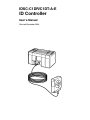
IDSC-C1DR/C1DT-A-E
ID Controller
USER’S MANUAL
IDSC-C1DR/C1DT-A-E
ID Controller
User’s Manual
Revised December 2004
iv
Notice:
OMRON products are manufactured for use according to proper procedures by a qualified operator
and only for the purposes described in this manual.
The following conventions are used to indicate and classify precautions in this manual. Always heed
the information provided with them. Failure to heed precautions can result in injury to people or damage to the product.
DANGER
Indicates an imminently hazardous situation which, if not avoided, will result in death or
serious injury.
! WARNING
Indicates a potentially hazardous situation which, if not avoided, could result in death or
serious injury.
! Caution
Indicates a potentially hazardous situation which, if not avoided, may result in minor or
moderate injury, or property damage.
!
OMRON Product References
All OMRON products are capitalized in this manual. The word “Unit” is also capitalized when it refers
to an OMRON product, regardless of whether or not it appears in the proper name of the product.
The abbreviation “Ch,” which appears in some displays and on some OMRON products, often means
“word” and is abbreviated “Wd” in documentation in this sense.
The abbreviation “PC” means Programmable Controller and is not used as an abbreviation for anything else.
Visual Aids
The following headings appear in the left column of the manual to help you locate different types of
information.
Note Indicates information of particular interest for efficient and convenient operation
of the product.
1, 2, 3...
1. Indicates lists of one sort or another, such as procedures, checklists, etc.
OMRON, 1995
All rights reserved. No part of this publication may be reproduced, stored in a retrieval system, or transmitted, in any
form, or by any means, mechanical, electronic, photocopying, recording, or otherwise, without the prior written permission of OMRON.
No patent liability is assumed with respect to the use of the information contained herein. Moreover, because OMRON is
constantly striving to improve its high-quality products, the information contained in this manual is subject to change
without notice. Every precaution has been taken in the preparation of this manual. Nevertheless, OMRON assumes no
responsibility for errors or omissions. Neither is any liability assumed for damages resulting from the use of the information contained in this publication.
v
vi
TABLE OF CONTENTS
SECTION 1
Features and System Configuration . . . . . . . . . . . . . . . . .
1-1
1-2
ID Controller Features . . . . . . . . . . . . . . . . . . . . . . . . . . . . . . . . . . . . . . . . . . . . . . . . . . . .
Overall ID Controller Procedure . . . . . . . . . . . . . . . . . . . . . . . . . . . . . . . . . . . . . . . . . . . .
SECTION 2
Hardware Components and Installation . . . . . . . . . . . . .
2-1
2-2
2-3
Component Names and Functions . . . . . . . . . . . . . . . . . . . . . . . . . . . . . . . . . . . . . . . . . . .
System Configuration and Installation . . . . . . . . . . . . . . . . . . . . . . . . . . . . . . . . . . . . . . . .
Installing the ID Controller . . . . . . . . . . . . . . . . . . . . . . . . . . . . . . . . . . . . . . . . . . . . . . . .
SECTION 3
Programming Device Operations . . . . . . . . . . . . . . . . . . .
3-1
3-2
3-3
3-4
3-5
Applicable Programming Devices . . . . . . . . . . . . . . . . . . . . . . . . . . . . . . . . . . . . . . . . . . .
Programming Console Preparations . . . . . . . . . . . . . . . . . . . . . . . . . . . . . . . . . . . . . . . . . .
Programming Console Operations . . . . . . . . . . . . . . . . . . . . . . . . . . . . . . . . . . . . . . . . . . .
LSS Operations . . . . . . . . . . . . . . . . . . . . . . . . . . . . . . . . . . . . . . . . . . . . . . . . . . . . . . . . . .
SSS Operations . . . . . . . . . . . . . . . . . . . . . . . . . . . . . . . . . . . . . . . . . . . . . . . . . . . . . . . . . .
SECTION 4
Data Areas . . . . . . . . . . . . . . . . . . . . . . . . . . . . . . . . . . . . .
4-1
4-2
4-3
Data Area Structure . . . . . . . . . . . . . . . . . . . . . . . . . . . . . . . . . . . . . . . . . . . . . . . . . . . . . .
Data Area Functions . . . . . . . . . . . . . . . . . . . . . . . . . . . . . . . . . . . . . . . . . . . . . . . . . . . . . .
ID Controller Area . . . . . . . . . . . . . . . . . . . . . . . . . . . . . . . . . . . . . . . . . . . . . . . . . . . . . . .
SECTION 5
ID Controller Functions and Setup . . . . . . . . . . . . . . . . .
5-1
5-2
5-3
5-4
5-5
5-6
ID Controller Setup . . . . . . . . . . . . . . . . . . . . . . . . . . . . . . . . . . . . . . . . . . . . . . . . . . . . . .
Basic Operations and I/O Processes . . . . . . . . . . . . . . . . . . . . . . . . . . . . . . . . . . . . . . . . . .
ID Communications . . . . . . . . . . . . . . . . . . . . . . . . . . . . . . . . . . . . . . . . . . . . . . . . . . . . . .
Advanced I/O Instructions . . . . . . . . . . . . . . . . . . . . . . . . . . . . . . . . . . . . . . . . . . . . . . . . .
Using Interrupts . . . . . . . . . . . . . . . . . . . . . . . . . . . . . . . . . . . . . . . . . . . . . . . . . . . . . . . . .
Communications . . . . . . . . . . . . . . . . . . . . . . . . . . . . . . . . . . . . . . . . . . . . . . . . . . . . . . . . .
SECTION 6
Programming . . . . . . . . . . . . . . . . . . . . . . . . . . . . . . . . . . .
6-1
6-2
6-3
6-4
6-5
Instruction Set . . . . . . . . . . . . . . . . . . . . . . . . . . . . . . . . . . . . . . . . . . . . . . . . . . . . . . . . . .
Basic Programming Concepts . . . . . . . . . . . . . . . . . . . . . . . . . . . . . . . . . . . . . . . . . . . . . .
ID Communications Instructions . . . . . . . . . . . . . . . . . . . . . . . . . . . . . . . . . . . . . . . . . . . .
Basic Instructions . . . . . . . . . . . . . . . . . . . . . . . . . . . . . . . . . . . . . . . . . . . . . . . . . . . . . . . .
Selected Special Instructions . . . . . . . . . . . . . . . . . . . . . . . . . . . . . . . . . . . . . . . . . . . . . . .
SECTION 7
Programming Examples . . . . . . . . . . . . . . . . . . . . . . . . . .
7-1
7-2
7-3
7-4
Recording Data . . . . . . . . . . . . . . . . . . . . . . . . . . . . . . . . . . . . . . . . . . . . . . . . . . . . . . . . . .
Displaying Worker Instructions . . . . . . . . . . . . . . . . . . . . . . . . . . . . . . . . . . . . . . . . . . . . .
Managing Production Histories . . . . . . . . . . . . . . . . . . . . . . . . . . . . . . . . . . . . . . . . . . . . .
Controlling Workpiece Flow . . . . . . . . . . . . . . . . . . . . . . . . . . . . . . . . . . . . . . . . . . . . . . .
SECTION 8
Internal Processing . . . . . . . . . . . . . . . . . . . . . . . . . . . . . .
8-1
8-2
8-3
Internal Processing . . . . . . . . . . . . . . . . . . . . . . . . . . . . . . . . . . . . . . . . . . . . . . . . . . . . . . .
Computing the Cycle Time . . . . . . . . . . . . . . . . . . . . . . . . . . . . . . . . . . . . . . . . . . . . . . . .
Execution Times for ID Communications . . . . . . . . . . . . . . . . . . . . . . . . . . . . . . . . . . . . .
1
2
7
9
10
15
28
33
34
34
37
52
53
55
56
57
60
63
64
69
73
86
94
110
121
122
126
134
140
145
155
156
157
158
159
161
162
163
165
vii
TABLE OF CONTENTS
SECTION 9
Troubleshooting . . . . . . . . . . . . . . . . . . . . . . . . . . . . . . . . .
9-1
9-2
9-3
9-4
9-5
9-6
9-7
9-8
9-9
Introduction . . . . . . . . . . . . . . . . . . . . . . . . . . . . . . . . . . . . . . . . . . . . . . . . . . . . . . . . . . . .
Programming Console Operation Errors . . . . . . . . . . . . . . . . . . . . . . . . . . . . . . . . . . . . . .
Programming Errors . . . . . . . . . . . . . . . . . . . . . . . . . . . . . . . . . . . . . . . . . . . . . . . . . . . . . .
User-defined Errors . . . . . . . . . . . . . . . . . . . . . . . . . . . . . . . . . . . . . . . . . . . . . . . . . . . . . .
Operating Errors . . . . . . . . . . . . . . . . . . . . . . . . . . . . . . . . . . . . . . . . . . . . . . . . . . . . . . . . .
ID Indicators . . . . . . . . . . . . . . . . . . . . . . . . . . . . . . . . . . . . . . . . . . . . . . . . . . . . . . . . . . . .
ID Controller Flags . . . . . . . . . . . . . . . . . . . . . . . . . . . . . . . . . . . . . . . . . . . . . . . . . . . . . . .
ID Error Logs . . . . . . . . . . . . . . . . . . . . . . . . . . . . . . . . . . . . . . . . . . . . . . . . . . . . . . . . . . .
Troubleshooting Flowcharts . . . . . . . . . . . . . . . . . . . . . . . . . . . . . . . . . . . . . . . . . . . . . . . .
171
172
173
173
174
175
177
178
179
181
Appendices
A
B
C
D
E
Standard Models . . . . . . . . . . . . . . . . . . . . . . . . . . . . . . . . . . . . . . . . . . . . . . . . . . . . . . . . . . .
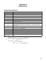
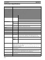
Specifications . . . . . . . . . . . . . . . . . . . . . . . . . . . . . . . . . . . . . . . . . . . . . . . . . . . . . . . . . . . . . .
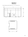
Dimensions . . . . . . . . . . . . . . . . . . . . . . . . . . . . . . . . . . . . . . . . . . . . . . . . . . . . . . . . . . . . . . . .
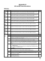
SR and AR Area Allocations . . . . . . . . . . . . . . . . . . . . . . . . . . . . . . . . . . . . . . . . . . . . . . . . . .
Extended ASCII . . . . . . . . . . . . . . . . . . . . . . . . . . . . . . . . . . . . . . . . . . . . . . . . . . . . . . . . . . . .
Glossary . . . . . . . . . . . . . . . . . . . . . . . . . . . . . . . . . . . . . . .
Index . . . . . . . . . . . . . . . . . . . . . . . . . . . . . . . . . . . . . . . . . .
Revision History . . . . . . . . . . . . . . . . . . . . . . . . . . . . . . . . .
viii
189
191
193
195
201
203
217
223
About this Manual:
This manual describes the installation and operation of the IDSC-C1DR-AE and IDSC-C1DT-AE ID Controllers and includes the sections described below. These ID Controllers provide complete Programmable
Controller (PC) functionality and use a electromagnetic coupling system to enable construction of noncontact information recognition (IDentification) systems.
Although this is the only manual provided specially for the ID Controllers, the following manuals must be
referenced as required when setting up, programming, installing, and operating an ID Controller System.
Information on
Constructing ID Systems, including information on Read/Write Heads, Data Carriers, etc.
Manual
V600 FA ID Sensor Serial Interface
Operation Manual (Z44)
V600 FA ID Sensor Parallel Interface
Operation Manual (Z45)
Programmable Controllers
CQM1 Programmable Controller
Programming Manual (W228)
Inputting programs or operating PCs
SYSMAC C-Series PC Ladder Support Software
Operation Manual (W237)
Please read this manual and the related manuals carefully and be sure you understand the information
provided before attempting to install and operate an ID Controller.
Section 1 describes the features of an ID Controller and the types of system configuration in which it can
be used.
Section 2 describes the components that make up an ID Controller and the procedures necessary to
install and mount an ID Controller.
Section 3 describes the Programming Console, Ladder Support Software (LSS) Operations, and SYSMAC Support Software (SSS) Operations used with an ID Controller System.
Section 4 describes the structure and use of the data areas used by the ID Controller.
Section 5 describes the functions of the ID Controller and the Setup that can be used to control those
functions.
Section 6 describes some of the ladder-diagram programming used to program the ID Controller. Refer
to the CQM1 Programming Manual for more information on ladder-diagram programming.
Section 7 provides four programming examples using ID communications instructions.
Section 8 described the processing that takes place within the ID Controller and explains how to calculate
the time required for program execution and related processing (called the scan time).
Section 9 describes how to diagnose and correct the hardware and software errors that can occur during
ID Controller operation and how to create user errors based on program execution.
The Appendices provide information on standard models, specifications, dimensions, SR and AR Area
allocations, and extended ASCII.
! WARNING Failure to read and understand the information provided in this manual may result in
personal injury or death, damage to the product, or product failure. Please read each
section in its entirety and be sure you understand the information provided in the section
and related sections before attempting any of the procedures or operations given.
ix
SECTION 1
Features and System Configuration
This section describes the features of an ID Controller and the types of system configuration in which it can be used.
1-1
1-2
ID Controller Features . . . . . . . . . . . . . . . . . . . . . . . . . . . . . . . . . . . . . . . . . . . . . . . . . . . . .
1-1-1 Overview . . . . . . . . . . . . . . . . . . . . . . . . . . . . . . . . . . . . . . . . . . . . . . . . . . . . . . . .
1-1-2 ID Controller Features . . . . . . . . . . . . . . . . . . . . . . . . . . . . . . . . . . . . . . . . . . . . . .
1-1-3 ID Controller Functions . . . . . . . . . . . . . . . . . . . . . . . . . . . . . . . . . . . . . . . . . . . . .
1-1-4 ID Controller Applications . . . . . . . . . . . . . . . . . . . . . . . . . . . . . . . . . . . . . . . . . .
Overall ID Controller Procedure . . . . . . . . . . . . . . . . . . . . . . . . . . . . . . . . . . . . . . . . . . . . .
2
2
3
3
4
7
1
Section 1-1
ID Controller Features
1-1
ID Controller Features
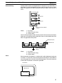
1-1-1 Overview
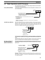
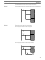
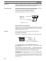
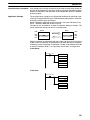
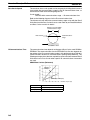
An ID Controller can be used to create a non-contact information system and is
equipped the complete functionality of a compact, high-speed Programmable
Controller (PC). Data is transferred between a Read/Write Head and Data Carriers in systems like the one shown in the following illustration.
ID Controller
Read/Write Head
Data Carrier
Moving object
Refer to the following page numbers for specific information.
2
• Hardware
24-VDC Inputs:
Transistor Outputs:
Contact Outputs:
Power Supply Wiring:
Read/Write Head Connections:
Page 21
Page 23
Page 24
Page 30
Page 31
• Data Areas:
Page 56
• Basic Operation and I/O:
Page 69
• Data Carrier Communications:
Page 73
• Communications Ports:
Page 110
• Data Carrier Memory:
Page 75
• ID Communications Instructions
DC READ/AUTOREAD:
DC WRITE/AUTOWRITE:
DC CLEAR:
DC MANAGE DATA:
All the Above Instructions:
Page 79
Page 80
Page 82
Page 83
Page 134
• Advanced I/O Instructions:
Page 86
• Interrupts:
Page 94
• Programming Console Operations:
Page 37
Section 1-1
ID Controller Features
1-1-2 ID Controller Features
• The ID Controller is equipped with an interface for electromagnetic-coupling ID
Sensors and one Read/Write Head can be connected. Communications (content read/write) with Data Carriers featuring this interface is performed by sequential programming commands.
• Interrupt functions are provided, and specific subroutines can be executed in
response to ID communications.
• The ID Controller can be used for various types of communications, such as
host links, NT links to PT, 1:1 links, and RS-232C.
• The controller is equipped with 32 I/O points (16 input points and 16 output
points).
• The details of up to 30 errors generated during communications with the Data
Carrier can be logged in response to errors in ID communication commands.
Other functions, such as online communications test, are available to test communications with Data Carriers.
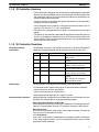
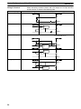
1-1-3 ID Controller Functions
ID Communications
Instructions
The following instructions are provided specifically for ID communications to
control data reception between the ID Controller and Data Carriers (DC).
Code
Mnemonic
61
IDRD
DC READ
Name
62
IDWT
DC WRITE
63
IDAR
DC AUTOREAD
64
IDAW
DC AUTOWRITE
65
IDCA
DC CLEAR
66
IDMD
DC MANAGE DATA
Function
Reads data from memory in the
Data Carrier.
Writes data to memory in the Data
Carrier.
Waits for approach of a Data
Carrier and then reads data.
Waits for approach of a Data
Carrier and then writes data.
Initializes memory in the Data
Carrier with the specified data.
Checks memory in the Data
Carrier.
Also manages the write life in
EEPROM Data Carriers.
ID Interrupts
The ID Controller is equipped with the following interrupt functions.
• ID communications response interrupt for ID communications responses.
• Input interrupts for external input signals
• Interval timer interrupts for internal timers
• High-speed counter interrupts for an internal counter
Communication Functions
Equipped with both a peripheral and an RS232 port, the ID Controller can communicate with external devices using the following methods
Host Link Communications or NT Links
Communications by Host Link commands is enabled by connecting the ID Controller to a Programmable Terminal (PT), personal computer or other device.
RS-232C Devices
Data can be read from bar code readers, measuring instruments, and other devices and data can be output to a printer.
1:1 Link Systems
Data areas can be linked by connecting the ID Controller to other ID Controller.
In this setup, operating status can be synchronized while the status of other
equipment can be monitored.
3
Section 1-1
ID Controller Features
32 I/O Points
ID Error Log
• Outputs:
16 contact outputs or 16 transistor outputs
• Inputs:
16 24-VDC inputs
The log of errors generated during ID communication is stored in the DM area in
the order generated (serial error log) or as statistical data by error type (error
statistics log). The time that an error was generated can also be stored in
memory if a Memory Cassette equipped with clock functions is provided.
Serial and error statistics logs can be checked from a Programming Console
connected to the ID Controller.
ID Communication Errors
Error
code
70
71
72
7A
7C
7D
PC Functions
Programming
Console message
COM.DC
VERIFY
NO DC
ADRS
R/WD
PROTCT
E
E
E
E
E
E
Meaning
Data Carrier communications error.
Data mismatch.
Data Carrier missing.
Data Carrier address error.
Read/Write Head not connected.
Protection error.
I/O and communication functions can be controlled with the ladder-diagram program in the PC. Advanced I/O instructions that input and output data with a
single instructions, macro instructions to call up subroutines, and differential
monitoring to monitor changes (via LSS/SSS) in signals are also provided to
help simplify programming and operation.
Note Refer to the CQM1 Programming and Operation Manuals for details on PC functions.
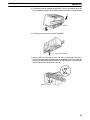
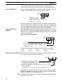
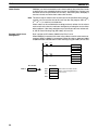
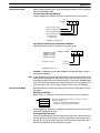
1-1-4 ID Controller Applications
The ID Controller facilitates the construction of non-contact ID systems that recognize data using and electromagnetic induction and can process the data using Programmable Controller (PC) functions. The contents of Data Carrier
memory can be read without direct connections or contact with Data Carriers
mounted on moving objects simply by connecting a Read/Write (R/W) Head to
the ID Controller, as shown in the following illustration.
ID Controller
Data Carrier
Read/Write Head
Data Carrier
Moving object
Moving object
4
Section 1-1
ID Controller Features
As a result, products or other articles can be distributed, and specific products
can be extracted automatically. (Refer to 7-4 Controlling Workpiece Flow.)
And since the ID Controller can write to Data Carriers, information such as
whether work was completed or work results can be recorded at any stage to the
Data Carrier of moving objects. (Refer to 7-1 Recording Data and 7-3 Managing
Production Histories.)
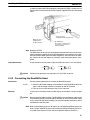
Connecting Programmable Terminals (PTs), shown in the following illustration,
to a ID Controller enables data confirmation, displays for work details applicable
in the ID system and other capabilities. (Refer to 7-2 Displaying Worker Instructions.)
ID Controller
Data Carrier
PT
Read/Write Head
Data Carrier
Moving object
Moving object
Data Recording
The ID Controller and Programmable Terminal can also be used to record data in
the Data Carrier. Workers can record data in the Data Carrier with a few simple
operations while confirming data details on a Programmable Terminal (PT)
fnscreen.
ID Controller
NT link to RS-232C port
Data registered for writing to Data Carrier
PT
Data input
Data Carrier
Workpiece
Read/
Write
Head
Workpieces
Worker
Data Carrier
Worker Instructions
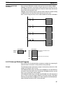
The ID Controller can read work data from Data Carriers and display the results
on lamp to direct line workers.
Part racks
Work start lamp
ID Controller
Lamp control signals
Workpiece
Data Carrier
#1
#2
#3
#4
#5
#6
#7
#8
Read/Write
Head
Worker
Assembly
End button
5
Section 1-1
ID Controller Features
Production History Control
The production history of products can be controlled in extreme detail at each
process by writing assembly and inspection results together with other information, such as time and line workers, to the Data Carriers. Clock functions can be
provided for time data if a clock-equipped Memory Cassette is used.
ID Controller
Instructions for writing inspection results
Data Carrier
Product
Inspection results
input panel
Read/Write
Head
Worker
Inspection
Distribution
The ID Controller can be used to distribute (route to another line by destination,
for example) articles on a conveyor.
In addition to distribution control with a simple mechanism like a pusher, the ID
Controller is also ideally suited to advanced distribution control using devices
that demand complex processing by servomotors and other equipment.
ID Controller
Data Carrier
Read/Write
Head
Motor control
Servomotor/controller
6
Product
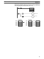
Overall ID Controller Procedure
1-2
Section 1-2
Overall ID Controller Procedure
The following flowchart illustrates the overall flow of using an ID Controller.
START
Design system.
Draw sequence diagrams.
Allocate Data Carrier memory.
Allocate I/O bits.
2-3 Installing the ID Controller
Section 4 Data Areas
Section 5 Using ID Control Features
Draw ladder-diagram program.
3-4 LSS Operations
3-5 SSS Operations
Connect and wire system.
Code program.
Apply power to ID Controller.
Input program.
Section 6 Programming Instructions
3-3 Programming Console Operations
Debug program.
Correct program.
Test system under trial operation.
Save program.
Operate system.
7
SECTION 2
Hardware Components and Installation
This section describes the components that make up an ID Controller and the procedures necessary to install and mount an ID
Controller.
2-1
2-2
2-3
Component Names and Functions . . . . . . . . . . . . . . . . . . . . . . . . . . . . . . . . . . . . . . . . . . . .
2-1-1 DIP Switch . . . . . . . . . . . . . . . . . . . . . . . . . . . . . . . . . . . . . . . . . . . . . . . . . . . . . . .
2-1-2 Indicators . . . . . . . . . . . . . . . . . . . . . . . . . . . . . . . . . . . . . . . . . . . . . . . . . . . . . . . .
2-1-3 ID Controller Operating Modes . . . . . . . . . . . . . . . . . . . . . . . . . . . . . . . . . . . . . . .
2-1-4 Memory Cassettes . . . . . . . . . . . . . . . . . . . . . . . . . . . . . . . . . . . . . . . . . . . . . . . . .
System Configuration and Installation . . . . . . . . . . . . . . . . . . . . . . . . . . . . . . . . . . . . . . . . .
2-2-1 Basic Configuration . . . . . . . . . . . . . . . . . . . . . . . . . . . . . . . . . . . . . . . . . . . . . . . .
2-2-2 Installation Precautions . . . . . . . . . . . . . . . . . . . . . . . . . . . . . . . . . . . . . . . . . . . . .
2-2-3 Terminal Blocks . . . . . . . . . . . . . . . . . . . . . . . . . . . . . . . . . . . . . . . . . . . . . . . . . . .
2-2-4 I/O Wiring Precautions . . . . . . . . . . . . . . . . . . . . . . . . . . . . . . . . . . . . . . . . . . . . .
2-2-5 I/O Specifications . . . . . . . . . . . . . . . . . . . . . . . . . . . . . . . . . . . . . . . . . . . . . . . . .
2-2-6 Connectable Devices . . . . . . . . . . . . . . . . . . . . . . . . . . . . . . . . . . . . . . . . . . . . . . .
2-2-7 Connecting External Devices via RS-232C Port . . . . . . . . . . . . . . . . . . . . . . . . . .
Installing the ID Controller . . . . . . . . . . . . . . . . . . . . . . . . . . . . . . . . . . . . . . . . . . . . . . . . .
2-3-1 Mounting the ID Controller . . . . . . . . . . . . . . . . . . . . . . . . . . . . . . . . . . . . . . . . . .
2-3-2 Wiring the Power Supply . . . . . . . . . . . . . . . . . . . . . . . . . . . . . . . . . . . . . . . . . . . .
2-3-3 Connecting the Read/Write Head . . . . . . . . . . . . . . . . . . . . . . . . . . . . . . . . . . . . .
10
10
11
12
13
15
15
16
18
18
21
25
26
28
28
30
31
9
Section 2-1
Component Names and Functions
2-1
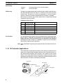
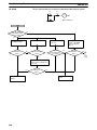
Component Names and Functions
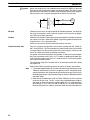
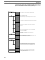
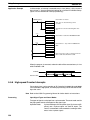
The following diagram shows the basic components that are used in general operation of the ID Controller.
Input Terminals and Indicators
Sixteen, 24-VDC input terminals including 4
interrupt inputs and up/down counter inputs.
Indicators
Display operating status.
Output Terminals and Indicators
Sixteen contact or 16 transistor
outputs.
Battery Set
Memory
Cassette
(optional)
Read/Write Head Connector
Used to connect the Read/Write
Head for the ID Sensor.
DIP switch
RS-232C Port
Used for communications with external
devices, such as a computer running
LSS/SSS, or other ID Controllers.
Power Supply and Indicator
Peripheral Port
Indicator lights when power is being sup- Used to connect to Peripheral Units such as a Proplied. External connection terminals.
gramming Console or a computer running LSS/SSS.
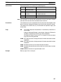
2-1-1 DIP Switch
The DIP switch is located under a cover on the front of the ID Controller as shown
above. The setting of these switches is described in the following table.
Pin
1
Setting
ON
OFF
Program Memory and read-only DM (DM 6144 to DM 6655) data
cannot be overwritten from a Peripheral Device.
Program Memory and read-only DM (DM 6144 to DM 6655) data
can be overwritten from a Peripheral Device.
Autoboot enabled. The contents of Memory Cassette will be
transferred to the ID Controller automatically at start-up.
Autoboot disabled.
ON
Programming Console messages will be displayed in English.
OFF
Programming Console messages will be displayed in the language stored in system ROM. (Messages will be displayed in
Japanese with the Japanese version of system ROM.)
ON
Expansion instructions set by user. Normally ON when using a
host computer for programming/monitoring.
Expansion instructions set to defaults.
OFF
2
3
4
ON
OFF
5
ON
OFF
6
Function
ON
OFF
RS-232C communications governed by default settings.
(1 start bit, even parity, 7-bit data, 1 stop bit, 2,400 bps)
RS-232C communications not governed by default settings.
The setting of pin 6 determines the ON/OFF status of AR 0712. If
pin 6 is ON
ON, AR 0712 will be ON and if pin 6 is OFF
OFF, AR 0712 will
be OFF.
Note All DIP switch pins except pin 3 are turned OFF at the factory.
10
Section 2-1
Component Names and Functions
2-1-2 Indicators
ID Controller indicators provide visual information on the general operation of
the ID Controller. Although not substitutes for proper error programming using
the flags and other error indicators provided in the data areas of memory, these
indicators provide ready confirmation of proper operation. ID Controller indicators are shown below and are described in the following table.
ID function indicators
RDY, ERR, T/R
RUN indicator (Green)
Output status indicators
0 1 2 3
Error/alarm
indicator (Red)
4 5 6 7
Input status indicators
8 9 10 11
12 13 14 15
Output inhibited indicator (Orange)
Peripheral port indicator (COM1) (Orange)
RS-232C port indicator (COM2) (Orange)
Indicator
RUN
(Green)
ERR/ALM
(Red)
Name
RUN indicator
Error/Alarm indicator
Function
Lights when the ID Controller is operating
normally.
Flashes when there is a non-fatal error.
The ID Controller will continue operating.
Lit when there is a fatal error. When this
indicator lights, the RUN indicator will go
off, ID Controller operation will be
stopped, and all outputs will be turned
OFF.
COM1
(Orange)
Peripheral port indicator
Flashes then the ID Controller is
communicating with another device via
the peripheral port.
COM2
(Orange)
RS-232C port indicator
Flashes when the ID Controller is
communicating with another device via
the RS-232C port.
OUT INH
(Orange)
Output inhibited indicator Lights when the Output OFF Bit,
SR 25215, is turned ON. All ID Controller
outputs will be turned OFF.
0, 1, 2 . . .
Input status indicators
Indicate the ON and OFF status of input
bits in IR 000.
0, 1, 2 . . .
Output status indicators
Indicate the ON and OFF status of output
bits in IR 100.
ID Function Indicators
RDY
(Green)
ERR (Red)
T/R
(Orange)
Operation Ready
Lit when ID functions are possible.
Error/Alarm
Lit when there is an error in the ID
Controller Setup or when operation stops
during communications.
ID Communications
Flashes when there is an error in ID
communications.
Lit when communications are taking place
with the Read/Write Head.
11
Section 2-1
Component Names and Functions
2-1-3 ID Controller Operating Modes
ID Controllers have three operating modes: PROGRAM, MONITOR, and RUN.
The ID Controller mode can be changed from the mode selector on the Programming Console.
Mode selector
MONITOR
RUN
PROGRAM
The key cannot be removed when the
mode selector is set to PROGRAM.
Note Some Programming Devices (e.g., the Programming Console) will clear the current display and display the new operating mode when the mode selector is
changed. You can change the mode without changing the display by first pressing the SHIFT Key and then changing the setting of the mode selector. When
changing between RUN and PROGRAM mode, press the SHIFT Key once and
change to MONITOR mode and then press the SHIFT Key again before switching to the final mode.
RUN Mode
RUN mode is used when operating the ID Controller in normal control conditions. Bit status cannot be force set or reset, and SVs, PVs, and data cannot be
changed online.
MONITOR Mode
MONITOR mode is used when monitoring program execution, such as making a
trial run of a program. The program is executed just as it is in RUN mode, but bit
status, timer and counter SV/PV, and the data content of most words can be
changed online. Output points will be turned ON when the corresponding output
bit is ON.
PROGRAM Mode
PROGRAM mode is used when making basic changes to the ID Controller program or settings, such as transferring, writing, editing, or checking the program,
or changing the ID Controller Setup. The program is not executed in PROGRAM
mode.
Mode Changes
The factors that determine the initial operating mode of the ID Controller (the
mode when the ID Controller is turned on) are listed below.
1, 2, 3...
1. No Devices mounted: RUN mode
If no Peripheral Devices are mounted to the ID Controller, the ID Controller
will enter RUN mode when turned ON unless the startup mode setting in the
ID Controller Setup (DM 6600) has been set to MONITOR or PROGRAM
Mode.
2. Programming Console mounted:
If the Programming Console is connected to the ID Controller when ID Controller power is applied, the ID Controller will enter the mode set on the Programming Console’s mode selector.
3. Other Peripheral Device mounted:
If a Programming Console is not mounted to the ID Controller, but another
Peripheral Device is connected to the ID Controller, the ID Controller will enter PROGRAM mode.
12
Section 2-1
Component Names and Functions
If the ID Controller power supply is already turned on when a Peripheral Device
is attached to the ID Controller, the ID Controller will stay in the same mode it was
in before the peripheral device was attached. If the Programming Console is
connected, the ID Controller will enter the mode set on the Programming Console’s mode selector once the password has been entered.
2-1-4 Memory Cassettes
Six Memory Cassettes are available as accessories to store the program or ID
Controller Setup. The following CQM1 Memory Cassettes are used for ID Controllers.
Note When pin 2 of the ID Controller’s DIP switch is ON, the contents of the Memory
Cassette will be transferred to the ID Controller automatically at start-up.
Memory
EEPROM
EPROM
Clock Function
Model
Comments
The Programming Console is
used to write to EEPROM
EEPROM.
(4K words)
No
CQM1-ME04K
Yes
CQM1-ME04R
No
CQM1-ME08K
Yes
CQM1-ME08R
The Programming Console is
used to write to EEPROM
EEPROM.
(8K words)
No
Yes
CQM1-MP08K
CQM1-MP08R
A PROM Writer is used to write
to EPROM
EPROM.
Memory Cassette Installation Follow the procedure below to install a Memory Cassette in the ID Controller.
! Caution
Always turn off power to the ID Controller before installing or removing a Memory
Cassette.
1, 2, 3...
1. Remove the mounting bracket from inside the memory cassette compartment.
2. Slide the Memory Cassette into the ID Controller on the tracks provided.
Press the Memory Cassette in so that the connectors fit securely.
Memory cassette
3. Replace the bracket as shown below and tighten the screw.
Mounting bracket
13
Section 2-1
Component Names and Functions
EEPROM Write Protection
! Caution
Turn on the write-protect switch on the EEPROM Memory Cassette to prevent
the program or ID Controller Setup from being deleted accidentally. Turn the
switch off when writing to the Memory Cassette.
Always turn off the ID Controller and remove the Memory Cassette when changing the write-protect switch setting.
Read/write
Read-only
(write-protected)
Note Flag AR 1302 will be ON when the write-protect switch is ON.
EPROM Version
The three EPROM Chips listed below can be used in the Memory Cassettes.
These Chips are made by OMRON.
EPROM version
Capacity
Access speed
Model number
27128
8K words
150 ns
ROM-ID-B
27256
16K words
150 ns
ROM-JD-B
27512
32K words
150 ns
ROM-KD-B
Be sure that the EPROM version set with the switch on the Memory Cassette
agrees with the EPROM version of the installed chip. Refer to the following diagram and table for the location of the switch and its settings.
ON
OFF
EPROM Version
Pin 1 Setting
Pin 2 Setting
27128
OFF
OFF
27256
ON
OFF
27512
ON
ON
Install an EPROM chip onto the Memory Cassette as shown in the following diagram.
14
System Configuration and Installation
2-2
Section 2-2
System Configuration and Installation
2-2-1 Basic Configuration
The basic components of an ID Controller System are shown in the following illustration.
Input Terminals
Output Terminals
(transistor or contact)
Power Supply
V600-series Read/Write
Head (R/W Head, Electromagnetic Coupling)
V600-series Data
Carrier (DC)
Read/Write Head Connector
Peripheral Port
(See note)
RS-232C Port
(See note)
Note These ports can be connected to a Programming Console (CQM1-PRO01-E or
C200H-PRO27-E) or to an IBM PC/AT or compatible computer (running Ladder
Support Software or SYSMAC Support Software).
ID Controller
I/O points:
Program capacity:
Data memory:
32
3.2K words
6K words
ID Communications
Connectable R/W Heads:
Data transmission capacity:
Communications instructions:
1
256 bytes max.
Six for ID communications
Power Supply
Voltage:
Power supply capacity:
100 to 240 VAC
3.6 A (18 W) at 5 VDC
Input Terminals
Number of inputs:
Voltage:
16
24 V
Output Terminals
See following table.
Item
Transistor outputs
Contact outputs
Number of outputs
16
16
Voltage
4.5 to 26.4 V
250 VAC/24 VDC
Max. switching capacity
0.3 A
2 A (8 A total)
15
System Configuration and Installation
Section 2-2
2-2-2 Installation Precautions
This section provides precautions for installing the ID Controller.
! Caution Static electricity can damage ID Controller components. Your body can carry an
electrostatic charge, especially when the humidity is low. Before touching the ID
Controller, be sure to first touch a grounded metallic object, such as a metal water pipe, in order to discharge any static build-up.
Ambient Conditions
Do not install the ID Controller in any of the following locations. Doing so will affect ID Controller life and may affect operating performance.
• Locations subject to ambient temperatures lower than 0°C or higher than
55°C, or 0°C to 45°C when a Programming Console is used.
• Locations subject to drastic temperature changes or condensation.
• Locations subject to ambient humidity lower than 10% or higher than 90%.
• Locations subject to corrosive or flammable gases.
• Locations subject to excessive dust (especially iron dust) or chloride.
• Locations that would subject the ID Controller to direct shock or vibration.
• Locations that would subject the ID Controller to water, oil, or chemical reagents.
• Locations exposed to direct sunlight.
• Do not install the ID Controller over heaters, transformers, high-capacity resistors, or other devices that generate heat.
High-voltage Equipment
To maintain safe operating conditions, locate the ID Controller as far away from
high-voltage equipment as possible.
Clearance
The ID Controller needs to have sufficient room to allow for I/O wiring, and additional room to ensure that the I/O wiring does not hamper cooling or does not
strike the cover to the control panel when it is closed. As a general rule, allow at
least 20 mm above and below the ID Controller.
Cooling Fan
A cooling fan is not always necessary, but may be needed in some installations.
Try to avoid mounting the ID Controller in a warm area or over a source of heat. A
cooling fan is needed if the ambient temperature may become higher than that
specified. If the ID Controller is mounted in an enclosure, install a cooling fan, as
shown in the following diagram, to maintain the ambient temperature within
specifications.
Fan
ID
Controller
Louver
16
System Configuration and Installation
External Wiring
Section 2-2
If power cables must be run alongside the I/O wiring (that is, in parallel with it), at
least 300 mm must be left between the power cables and the I/O wiring as shown
below. This applies to all cables carrying 10 A or less at 400 V or 20 A or less at
220 V.
Low current cable
1
300 mm min.
Control cable
2
Power cable
300 mm min.
3
Class-3 ground (to 100 Ω
or less)
Where:
1 = I/O wiring
2 = General control wiring
3 = Power cables
If the I/O wiring and power cables must be placed in the same duct (for example,
where they are connected to the equipment), they must be shielded from each
other using grounded metal plates.
Metal plate (iron)
200 mm min.
1
2
3
Class-3 ground (to 100 Ω
or less)
Where:
Noise
1 = I/O wiring
2 = General control wiring
3 = Power cables
Do not mount the ID Controller in a control panel in which high-power equipment
is installed,. To avoid noise, make sure the point of installation is at least 200 mm
away from power lines as shown in the following diagram. Ensure that the plate
to which the ID Controller is mounted is grounded.
Power lines
200 mm min.
ID Controller
200 mm min.
17
System Configuration and Installation
Mounting Direction
Section 2-2
Always mount the ID Controller with the cooling vents facing up. Never mount it
on it’s side or end.
Correct
Wrong
Wrong
2-2-3 Terminal Blocks
The I/O Controller’s terminal blocks are removable. Be sure that the connector
tabs are in the locked position, as shown in the following diagram.
To remove the terminal block, push the connector tabs to the sides and lift the
terminal block off of the connector, as shown in the following diagram.
Open the tabs as widely
as necessary.
Crimp connectors for I/O wiring should be less than 6.2 mm wide (M3).
6.2 mm max.
! Caution
6.2 mm max.
Forked crimp connectors are required by UL and CSA standards.
2-2-4 I/O Wiring Precautions
The following must be considered when connecting electrical devices to I/O terminals: leakage currents, inrush currents, noise, and inductive loads
! Caution
Tighten the terminal screws to a torque of 0.5 to 0.6 Nm.
! WARNING Do not apply voltages exceeding the maximum permissible input voltage to
inputs nor voltages exceeding the switching capacity to output. Doing so may
result in damage or destruction of the ID Controller or may result in fire.
Leakage Current (24 VDC)
18
A leakage current can cause false inputs when using 2-wire sensors (proximity
switches or photoelectric switches) or limit switches with LEDs on 24-VDC inputs.
System Configuration and Installation
Section 2-2
If the leakage current exceeds 1.3 mA, insert a bleeder resistor in the circuit to
reduce the input impedance, as shown in the following diagram.
Input power
supply
R = 7.2/(2.4I–3) kΩ max.
W = 2.3/R W min.
IDSC
R
Bleeder resistor
2-wire method
sensor, etc.
I: Device’s leakage current (mA)
R: Bleeder resistance (kΩ)
W: Bleeder resistor’s power rating (W)
The equations above were derived from the following equation:
I
Input voltage (24)
R Input current (10)
Input voltage (24)
R + Input current (10)
≤ OFF voltage (3)
W ≥ Input voltage (24)/R Input voltage (24) tolerance (4)
Inrush Current (Transistor)
The following diagram shows two methods that can be used to reduce the large
inrush current caused by certain loads, such as incandescent light bulbs, when
connected to transistor outputs
Example 1
Example 2
OUT
OUT
R
R
COM
COM
Generating a dark current (about 1/3 of the
rated current) through the incandescent bulb.
Inserting a regulating resistance.
Be careful not to damage the output transistor.
Noise on Input Signal Lines
I/O cables must be placed in separate ducts or wiring tubes both inside and outside of the control panel, as shown in the following diagram.
ÉÉÉÉÉÉ
ÉÉÉÉÉÉ ÉÉÉÉÉÉÉÉ
ÉÉÉÉÉÉÉÉ
ÉÉÉÉÉÉÉÉ
ÉÉÉÉÉÉÉÉ ÉÉÉÉÉÉ
ÉÉÉÉÉÉÉÉ ÉÉÉÉÉÉ
1
1
2
1
2
2
Floor ducts
Wiring tubes
(1): I/O Cables
(2): Power lines
Suspended ducts
Inductive Loads
When connecting an inductive load to an I/O terminal, connect a diode in parallel
with the load. The diode should satisfy the following requirements:
1, 2, 3...
1. Peak reverse-breakdown voltage must be at least 3 times the load voltage.
2. Average rectified current must be 1 A.
Inputs
Outputs
IN
Diode
COM
OUT
DC input
Contact output
Transistor output
Diode
COM
19
System Configuration and Installation
Wiring I/O Terminal
Device output type
Contact output
Section 2-2
When connecting an external device with a DC output to a DC input terminal,
wire the device as shown in the following table.
Circuit Diagram (External device on left; input terminals on right
Relay
IN
COM(+)
NPN open collector
Sensor
+
Sensor power
supply
Output
IN
COM(+)
0V
Use the same power supply
for the input and sensor.
NPN current output
Constant current
circuit
+
Output
0V
IN
Sensor power
supply
+
COM(+)
PNP current output
+
Sensor power
supply
Output
IN
0V
COM(–)
Voltage output
COM (+)
Output
0V
20
IN
Sensor power
supply
System Configuration and Installation
Section 2-2
2-2-5 I/O Specifications
24-VDC Inputs (16 pts)
Item
Specification
Model
IDSC-C1Dj-A-E
Input Voltage
24 VDC +10%/–15%
Input Impedance
IN4 and IN5: 2.2 kΩ; other inputs: 3.9 kΩ
Input Current
IN4 and IN5: 10 mA typical; other inputs: 6 mA typical (at 24 VDC)
ON Voltage
14.4 VDC min.
OFF Voltage
5.0 VDC max.
ON Delay
Default: 8 ms max. (can be set between 1 and 128 ms in ID Controller Setup; see note)
OFF Delay
Default: 8 ms max. (can be set between 1 and 128 ms in ID Controller Setup; see note)
No. of Inputs
16 points (16 inputs/common, 1 circuit)
Circuit Configuration
IN0
to
IN15
Input
LED
3.9 kΩ
(2.2 kΩ)
COM
Internal
Circuits
560 Ω
Note Figures in parentheses are for IN4 and IN5.
The input power supply polarity may be connected in either direction.
Terminal Connections
0
1
B0
A0
2
3
B1
A1
4
5
B2
A2
6
7
B3
A3
8
9
B4
A4
10
11
B5
A5
12
13
B6
A6
14
15
B7
A7
COM
–
COM
B8
A8
–
Note IN0 through IN3 can be set for use as input interrupts in the ID Controller Setup.
The ON and OFF delays for input interrupts are fixed at 0.1 ms max. and 0.5 ms
max., respectively. IN4 through IN6 can be set for use as high-speed counter
interrupts. The delays for high-speed counter interrupts are shown in the following table.
Input
IN4 (A)
IN5 (B)
IN6 (Z)
Increment input mode
5 KHz
Normal input
Differential phase mode
2.5 KHz
ON: 100 ms min. required; OFF delay: 500 ms min. required
21
System Configuration and Installation
Section 2-2
The minimum response pulses will be as follows:
Input A (IN4), Input B (IN5)
Increment Mode (5 kHz max.)
200 µs min.
90 µs min.
ON
Phase A
OFF
90 µs min.
Phase-input Difference Mode (2.5 kHz max.)
400 µs min.
ON
Phase A
OFF
ON
Phase B
OFF
T1
T2
T3
T4
T1, T2, T3, T4: 90 µs min.
Input Z (IN6)
100 µs min.
ON
Phase Z
OFF
500 µs min.
22
System Configuration and Installation
Section 2-2
Transistor Outputs (16 pts)
Item
Specification
Model
IDSC-C1DT-A-E
Max. Switching Capacity
50 mA at 4.5 VDC to 300 mA at 26.4 V (see diagram below)
Leakage Current
0.1 mA max.
Residual Voltage
0.8 V max.
ON Delay
0.1 ms max.
OFF Delay
0.4 ms max.
No. of Outputs
16 points (16 points/common, 1 circuit)
Internal Current
Consumption
Fuse
170 mA max. at 5 VDC
Service Power Supply
40 mA min. at 5 to 24 VDC "10% (2.5 mA number of ON points)
5 A (one per common), one only (Fuse is not user replaceable.)
Circuit Configuration
+V
Output
LED
OUT0
to
OUT15
Internal
Circuits
COM
Fuse
5A
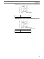
Max. Switch Capacity (per Point)
4.5
to
26.4
VDC
Max. Switch Capacity (Total)
5.0
4.8
Ic max. (A)
Ic max. (mA)
300
3.0
2.8
50
4.5
20.4
26.4 +V (V)
External power supply voltage
0
Terminal Connections
0
1
B0
A0
2
3
B1
A1
4
5
B2
A2
6
7
B3
A3
8
9
B4
A4
10
11
B5
A5
12
13
B6
A6
14
15
B7
A7
+DC
COM
–
45
55
(_C)
Ambient temperature
B8
A8
23
System Configuration and Installation
Section 2-2
Contact Outputs (16 pts)
Item
Specification
Model
IDSC-C1DR-A-E
Max. Switching
Capacity
2 A, 250 VAC (cosφ= 1)
2 A, 250 VAC (cosφ= 0.4)
2 A, 24 VDC (8 A total)
10 mA, 5 VDC
Min. Switching
Capacity
Relay
Service Life of
Relay
ON Delay
OFF Delay
No. of Outputs
Internal Current
Consumption
Circuit
Configuration
G6D-1A
Electrical: 300,000 operations (resistive load) 100,000 operations (inductive load)
Mechanical: 20,000,000 operations
10 ms max.
5 ms max.
16 points (16 points/common, 1 circuit))
850 mA max. at 5 VDC
Output
LED
OUT0
OUT15
Internal
Circuits
COM
Terminal
Connections
0
1
B0
A0
2
3
B1
A1
4
5
B2
A2
6
7
B3
A3
8
9
B4
A4
10
11
B5
A5
12
13
B6
A6
14
15
B7
A7
COM
COM
24
B8
A8
Maximum
250 VAC: 2 A
24 VDC: 2 A
System Configuration and Installation
Section 2-2
2-2-6 Connectable Devices
Memory Cassettes
Memory
EEPROM
EPROM ((socket only)
y)
Battery Set
Name
Read/Write Heads and Data
Carriers
Model
CQM1-ME04K
CQM1-ME04R
CQM1-ME08K
CQM1-ME08R
CQM1-MP08K
CQM1-MP08R
Clock
No
Yes
No
Yes
No
Yes
Capacity
4K words
8K words
8K words
Model
Battery Set
3G2A9-BAT08
Name
Read/Write Head
Model
V600-H07
Comments
30.5 m max.
V600-H11/H51/H52
50.5 m max.
V600-DjjRjj
Built-in lithium battery
V600-DjjPjj
No battery
Data Carrier
Note Not all combinations of Data Carrier and Read/Write Head are possible. Refer to
the following manuals for details: V600 FA ID Sensor Serial Interface Operation
Manual (Z44-E1-2) and V600 FA ID Sensor Parallel Interface Operation Manual
(Z45-E1-2).
Programming Devices
The ID Controller can be programmed and operated either from an IBM PC/AT
or compatible running the LSS/SSS or from a Programming Console.
Connect the computer using the illustrated cables. The computer must run the
Ladder Support Software (LSS) version 3 or later (on 3.5” floppy disks:
C500-SF312-EV3; on 5” floppy disks: C500-SF711-EV3), or SYSMAC Support
Software (SSS) (C500-ZL3AT1-E).
RS-232C
connector
CQM1-CIF02 Connecting Cable
Peripheral port
RS-232C cable (provided by user)
RS-232C
connector
RS-232C port
25
System Configuration and Installation
Section 2-2
Connect the Programming Console using the illustrated cables.
CQM1 Programming Console
CQM1-PRO01-E
Use enclosed cable.
Peripheral port
C-series Programming Console
C200H-PRO27-E
Connecting Cable:
C200H-CN222 (2 m)
C200H-CN422 (4 m)
Peripheral port
2-2-7 Connecting External Devices via RS-232C Port
Various types of devices can be connected to the ID Controller via the RS-232C.
A few examples are shown in the following illustration.
Host link
RS-232C Devices
Personal computer
Printer
Bar Code Reader
PT
26
1 to 1 link
System Configuration and Installation
Section 2-2
RS-232C Port Specifications
The specifications for the RS-232C port are given below. Devices that meet
these specifications can be connected.
Connector Pin Assignments
Pin assignments for the RS-232C port are given in the following table.
Pin
1
6
9
5
Personal Computer
Abbreviation
Name
Direction
1
FG
Field ground
---
2
SD (TXD)
Send data
Output
3
RD (RXD)
Receive data
Input
4
RS (RTS)
Request to send
Output
5
CS (CTS)
Clear to send
Input
6
---
Not used.
---
7
---
Not used.
---
8
---
Not used.
---
9
SG
Signal ground
---
Connector fitting
FG
Field ground
---
The connections between the ID Controller and a personal computer are illustrated below as an example.
ID Controller
Personal Computer
Signal
Pin
No.
Pin
No.
Signal
FG
1
1
–
SD
2
2
RD
RD
3
3
SD
RS
4
4
DTR
CS
5
5
SG
–
6
6
DSR
–
7
7
RS
–
8
8
CS
SG
9
9
–
Shielded cable
One-to-one Link Connections The RS-232C port can be connected to the same port on another ID Controller to
create a data link. Wire the cable as shown in the diagram below.
ID Controller
ID Controller
Signal
Abb.
Pin
No.
Pin
No.
Signal
Abb.
FG
1
1
FG
SD
2
2
SD
RD
3
3
RD
RS
4
4
RS
CS
5
5
CS
–
6
6
–
–
7
7
–
–
8
8
–
SG
9
9
SG
Ground the FG terminals of ID Controller at a resistance of less than 100 Ω.
27
Installing the ID Controller
Section 2-3
Applicable Connectors
The following connectors are applicable. One plug and one hood are included
with the ID Controller.
Plug: XM2A-0901 (OMRON) or equivalent
Hood: XM2S-0901 (OMRON) or equivalent
Port Specifications
Item
2-3
Specification
Communications method
Half duplex
Sync
Start-stop
Baud rate
1,200, 2,400, 4,800, 9,600, or 19,200 bps
Transmission method
Point to point
Transmission distance
15 m max.
Interface
EIA RS-232C
Installing the ID Controller
2-3-1 Mounting the ID Controller
An ID Controller must be installed on DIN Track and secured with the DIN Track
Brackets shown below.
DIN Track
(PFP-50N or PFP-100N)
DIN Track Brackets (PFP-M)
Use the following procedure to install an ID Controller on DIN Track.
1, 2, 3...
1. Mount the DIN Track securely to the control board or inside the control panel
using screws in at least 3 separate locations.
2. Release the pins on the backs of the ID Controller. These pins lock the ID
Controller to the DIN Track.
DIN track
mounting pin
28
Unlock
Installing the ID Controller
Section 2-3
3. Fit the back of the ID Controller onto the DIN Track by inserting the top of the
track and then pressing in at the bottom of the ID Controller, as shown below.
DIN track
4. Lock the pins on the backs of the ID Controller.
DIN track mounting pin
5. Install a DIN Track Bracket on each side of the ID Controller. To install a
bracket, hook the bottom of the Bracket on the bottom of the track, rotate the
Bracket to hook the top of the Bracket on the top of the track, and then tighten the screw to lock the Bracket in place.
DIN Track Brackets
29
Installing the ID Controller
Section 2-3
2-3-2 Wiring the Power Supply
The following diagram shows the proper connection to an AC power supply. The
AC voltage should be between 100 and 240 VAC with an allowable range of 85 to
264 VAC.
The cross-sectional area of each wire must be 2 mm2 min.
Insulating transformer
Breaker
AC power supply
An insulating transformer greatly
reduces the noise that may be
induced between the power line and
ground. Do not ground the secondary
side of the insulating transformer.
Twist the wires.
! Caution
Wiring Precautions for
Ground Wires
Be sure that the AC power supply voltage remains within the allowed fluctuation
range of 85 to 264 VAC. Exceeding this range may destroy the ID Controller.
Wire the grounding wires according to the diagram shown below. The ID Controller with the lot number jjZ5 manufactured in December 1995 and later is
provided with the LG-GR short-circuit bar and the DIN-track cable.
Terminal Block for External Connections
The following diagram shows the terminal blocks for the external power supply.
AC
Use an AC power supply
input between 100 and 240 VAC.
LG
Noise filter neutral terminal
GR
Protective earth terminal
The wire used should be at least 2 mm2. Provide the grounding point as close to
the ID Controller as possible.
! WARNING LG:
Noise filter neutral terminal. Short-circuit the LG terminal and GR terminals
using the attached short-circuit bar and ground them at a resistance of less than
100 Ω to reduce noise and prevent electric shock.
! WARNING GR:
Protective earth terminal. Connect to a separate ground wire of at least 2 mm2 to
ground the terminal at a resistance of less than 100 Ω to prevent electric shock.
! Caution
Avoid sharing the grounding wire with other equipment or attaching to the beam
of a building, otherwise it may cause an adverse effect.
Correct
ID Controller
30
Incorrect
Other
equipment
ID Controller
Other
equipment
Installing the ID Controller
Section 2-3
In order to improve the Electro Magnetic Compatibility (EMC), connect the LG
terminal to the screw on the end plate using the supplied DIN-track connecting
cable.
Short-circuit bar
(Supplied with the ID Controller)
DIN-track cable
(Supplied with
the ID Controller)
Grounding wire
(Use a wire of at least 2 mm2
to ground at a resistance of
less than 100 Ω.)
Note Definition of EMC:
The EMC refers to the capacity of equipment represented in terms of emission,
which indicates the degree to which electromagnetic waves produced by equipment do not affect other communications equipment, and also in terms of immunity, which indicates the degree of resistance against electromagnetic disturbance.
Crimp connectors for the power supply should be less than 7 mm wide (M3.5).
Crimp Connectors
7 mm max.
! Caution
7 mm max.
Forked crimp connectors are required by UL and CSA standards.
2-3-3 Connecting the Read/Write Head
Connection
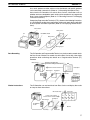
Use the following procedure to connect the Read/Write Head.
1, 2, 3...
1. Hold on to the rubber molding at the connector of the Read/Write Head and
align it with the keyed slot on the connector on the ID Controller.
2. Press in firmly on the connector until it clicks into place.
Removal
To remove the connector, hold onto the ring on the connector and pull straight
out.
! Caution
Do not pull on the rubber molding. The Read/Write Head connector cable cannot
be removed by pulling out on the rubber molding; you must hold onto the sliding
ring. If you pull on the rubber molding, you may damage the connector or break
connections inside the cable.
Note Refer to the following manuals for details on installing Read/Write Heads and
Data Carriers: V600 FA ID Sensor Serial Interface Operation Manual (Z44-E1-2)
and V600 FA ID Sensor Parallel Interface Operation Manual (Z45-E1-2)
31
SECTION 3
Programming Device Operations
This section describes the Programming Console, Ladder Support Software (LSS) Operations, and SYSMAC Support Software (SSS) Operations used with an ID Controller System.
3-1
3-2
3-3
3-4
3-5
Applicable Programming Devices . . . . . . . . . . . . . . . . . . . . . . . . . . . . . . . . . . . . . . . . . . . .
Programming Console Preparations . . . . . . . . . . . . . . . . . . . . . . . . . . . . . . . . . . . . . . . . . . .
Programming Console Operations . . . . . . . . . . . . . . . . . . . . . . . . . . . . . . . . . . . . . . . . . . . .
3-3-1 Testing ID Communications . . . . . . . . . . . . . . . . . . . . . . . . . . . . . . . . . . . . . . . . .
3-3-2 Reading the ID Error Log . . . . . . . . . . . . . . . . . . . . . . . . . . . . . . . . . . . . . . . . . . .
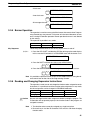
3-3-3 Clearing Memory . . . . . . . . . . . . . . . . . . . . . . . . . . . . . . . . . . . . . . . . . . . . . . . . . .
3-3-4 Reading/Clearing Error Messages . . . . . . . . . . . . . . . . . . . . . . . . . . . . . . . . . . . . .
3-3-5 Buzzer Operation . . . . . . . . . . . . . . . . . . . . . . . . . . . . . . . . . . . . . . . . . . . . . . . . . .
3-3-6 Reading and Changing Expansion Instructions . . . . . . . . . . . . . . . . . . . . . . . . . . .
3-3-7 Reading and Changing the Clock . . . . . . . . . . . . . . . . . . . . . . . . . . . . . . . . . . . . .
3-3-8 Setting and Reading a Program Memory Address . . . . . . . . . . . . . . . . . . . . . . . . .
3-3-9 Inserting and Deleting Instructions . . . . . . . . . . . . . . . . . . . . . . . . . . . . . . . . . . . .
3-3-10 Entering or Editing Programs . . . . . . . . . . . . . . . . . . . . . . . . . . . . . . . . . . . . . . . .
3-3-11 Checking the Program . . . . . . . . . . . . . . . . . . . . . . . . . . . . . . . . . . . . . . . . . . . . . .
3-3-12 Bit, Digit, Word Monitor . . . . . . . . . . . . . . . . . . . . . . . . . . . . . . . . . . . . . . . . . . . .
3-3-13 Hex-ASCII Display Change . . . . . . . . . . . . . . . . . . . . . . . . . . . . . . . . . . . . . . . . .
3-3-14 Displaying the Cycle Time . . . . . . . . . . . . . . . . . . . . . . . . . . . . . . . . . . . . . . . . . .
3-3-15 Force Set, Reset . . . . . . . . . . . . . . . . . . . . . . . . . . . . . . . . . . . . . . . . . . . . . . . . . . .
3-3-16 Clear Force Set/Reset . . . . . . . . . . . . . . . . . . . . . . . . . . . . . . . . . . . . . . . . . . . . . . .
3-3-17 Binary Monitor . . . . . . . . . . . . . . . . . . . . . . . . . . . . . . . . . . . . . . . . . . . . . . . . . . .
3-3-18 Hexadecimal, BCD Data Modification . . . . . . . . . . . . . . . . . . . . . . . . . . . . . . . . .
3-3-19 Binary Data Modification . . . . . . . . . . . . . . . . . . . . . . . . . . . . . . . . . . . . . . . . . . .
LSS Operations . . . . . . . . . . . . . . . . . . . . . . . . . . . . . . . . . . . . . . . . . . . . . . . . . . . . . . . . . .
SSS Operations . . . . . . . . . . . . . . . . . . . . . . . . . . . . . . . . . . . . . . . . . . . . . . . . . . . . . . . . . . .
34
34
37
37
38
39
40
41
41
42
43
44
45
47
47
49
49
49
50
50
51
51
52
53
33
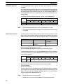
Programming Console Preparations
3-1
Section 3-2
Applicable Programming Devices
The following Programming Devices can be used with an ID Controller System.
Programming Consoles
CQM1-PRO01-E or C200H-PRO27-E
Ladder Support Software
Version 3 or later running on an IBM PC/AT or compatible:
C500-SF312-EV3 (on 3.5” floppy disks)
C500-SF711-EV3 (on 5” floppy disks)
Note Be sure to perform the operations listed in 3-4 LSS Operations before using the
LSS or 3-5 SSS Operations before using the SSS for an ID Controller.
3-2
Programming Console Preparations
This and the following section provide an introduction to the main operations
possible on a Programming Console, although there are other operations that
can also be used for an ID Controller System. Refer to the CQM1 Programmable
Controller Operation Manual (W226-E1-2A) for details on other possible operations.
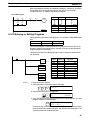
Key Sequences
Graphic key sequences are provided for Programming Console operations. Just
press the keys in the order they are shown. Many of the keys show example data
they should be replace with actual data during operation.
Initial Display
Most key sequences are given assuming that the Programming Console is
showing the initial display. If the initial display is not on the Programming Console when you want to start a new operation, just press the CLEAR Key repeatedly until you reach the initial display.
Components and Functions
There are two Programming Consoles that can be used with the ID Controller:
the CQM1-PRO01-E and the C200H-PRO27-E. The key functions for these
Programming Consoles are identical.
Press the Shift Key to input a letter shown in the upper-left corner of the key or
the upper function of a key that has two functions. For example, the
CQM1-PRO01-E’s AR/HR key can specify either the AR or HR Area; press and
release the Shift Key and then press the AR/HR Key to specify the AR Area.
C200H-PRO27-E
(Use a C200H-CN222 (2 m)
or C200H-CN422 (4 m)
Connecting Cable.)
CQM1-PRO01-E
(A 2-m connecting cable is
included.)
LCD display
Mode
selector
ID Controller operating
mode
Instruction
keys
Numeric
keys
Operation
keys
34
Programming Console Preparations
! Caution
Section 3-2
When turning on the ID Controller, set it to PROGRAM mode using the mode
selector as described in 2-1-3 ID Controller Operating Modes unless you have a
specific reason to use another mode. If the ID Controller is set to RUN or MONITOR mode, the program will be executed when it is turned on, possibly causing
a ID Controller-controlled system to begin operation.
Note The following three sets of keys are labeled differently on the CQM1-PRO01-E
and the C200H-PRO27-E. The operation of the two keys in each pair are identical.
CQM1-PRO01-E
C200H-PRO27-E
AR
HR
HR
PLAY
SET
SET
REC
RESET
RESET
Connecting the
Programming Console
Connect the Programming Console’s connecting cable to the ID Controller’s peripheral port, as shown below. Refer to 2-2-6 Connectable Devices for details on
connections.
Peripheral port
Monitoring Errors
The following key sequence can be used to read the ID communications error
log any time during ID Controller operation. The ID Controller may be in any operating mode.
CLR
ID Function Test
SHIFT
CLR
MONTR
1
↑
2
↓
The Programming Console can be used to test ID communications. The ID Controller must be in PROGRAM mode for this set to be carried out.
1, 2, 3...
1. Turn bits SR 23208 and SR 23209 ON and then OFF from the Programming
Console to execute the test.
Data will be written and read from specific addresses in the Data Carrier at
1-second intervals and any errors occurring during the test will be recorded
in word SR 234.
2. Read the contents of SR 234 to check the results of the test.
Other Operations
Refer to the next section for other operations or to the CQM1 Programmable
Controller Operation Manual.
35
Programming Console Preparations
Section 3-2
The basic operations required to prepare for programming are listed below.
Preparatory Operations
1, 2, 3...
1. Set the Programming Console’s mode selector to PROGRAM mode.
2. Enter the password by pressing the CLR and then the MONTR Key.
At this point, the SHIFT and then the 1 key can be pressed to turn on and off
the Programming Console’s buzzer. Refer to page 41.
3. If you are going to input a new program, clear the ID Controller’s memory by
pressing the CLR, SET, NOT, RESET, and then the MONTR Key. Refer to
page 39.
4. Display and clear any error messages by pressing the CLR, FUN, and then
the MONTR Key. Continue pressing the MONTR Key until all error messages have been cleared. Refer to page 40.
5. Press the CLR Key to bring up the initial programming display (program address 00000).
Changing Displays
The following diagram shows which keys to press in order to change Programming Console displays.
Example mode display (connected to ID Controller)
{PROGRAM}
CLR
BZ
SHIFT
The ID Controller’s operating mode will be displayed.
CLR
(or switch modes)
Initial programming display
00000
CLR
Press several times.
(See note.)
Various operational displays
Note When cancelling an operation or beginning operation, press the CLR Key several times to return to the initial display.
After the SHIFT Key is pressed, changing the mode by means of the modechange switch will cause the mode to change while retaining the current display.
When switching between RUN and PROGRAM, first go into MONITOR and
press the SHIFT Key again.
36
Programming Console Operations
3-3
Section 3-3
Programming Console Operations
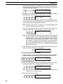
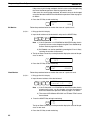
3-3-1 Testing ID Communications
This operation can be used to show the status of errors generated by executing
either a read or a write communications operation repeatedly every second for a
specific Data Carrier address. In the read test, one byte is read from the Data
Carrier repeatedly, while in the write test one byte is written to the Data Carrier
repeatedly. This operation is possible in PROGRAM mode only.
RUN
MONITOR
PROGRAM
No
No
OK
Note Data contained in the Data Carrier will not be overwritten, so the test can be used
for checks and other operations at system startup. At the same time, this function can also perform various adjustment tests, such as on-site adjustment of the
distance between the Data Carriers and the Read/Write Head.
1, 2, 3...
1. Monitor the content of word SR 234 in the ID controller.
CH
SHIFT
*
C
2
D
3
E
4
MONTR
c234
0000
2. Display bit SR 23209, and select the test mode (read or write) by turning
SR 23209 ON or OFF with the Set or Reset Key. (A read test is specified in
the following example.)
Read test: Turn OFF SR 23209.
Write test: Turn ON SR 23209.
SHIFT
CONT
C
#
2
D
3
C
2
REC
RESET
A
0
9
MONTR
23209 c234
OFF 0000
3. Display bit SR 23208 and turn it ON to start the test.
SHIFT
CONT
#
C
2
D
3
C
2
PLAY
SET
A
0
8
MONTR
23208 23209 c234
ON
OFF FFFF
During the test, the T/R indicator for the ID function will flash, and the test
results will be placed in word SR 234, as shown below.
FFFF: ID communication in progress
0x00: Normal end
0xxx: Error end
4. Refer to ID Communications Errors on page 178 for the meaning of error
messages and error codes.
5. When the next communication is executed normally, the error display will
automatically leave the screen.
6. Turn off bit 23208 to cancel the test or before shifting to the another operation. The following display shows a normal ending for the test.
REC
RESET
! Caution
23208 23209 c234
OFF
OFF 0100
Do not change ID Controller operating mode while the test function is being
executed (i.e., while SR 23208 is ON).
37
Programming Console Operations
Section 3-3
3-3-2 Reading the ID Error Log
When the ID Controller is running in the operating mode, information on various
types of errors is stored in the DM area in the ID Error Log and in the ID Error
Statistics Log. This information can be displayed on the Programming Console
as error messages.
ID Error Log
The last 30 errors are displayed in order of the error log data number.
ID Error Statistics Log
The numbers of ID communications errors generated are displayed by the type
of error.
Note The ID Error Log and ID Error Statistics Log may or may not be stored in memory
depending on ID Controller Setup. ID error log information is stored in one of two
ways, leaving either the newest error or the first 30 errors. Refer to 5-1 ID Controller Setup for details.
Displaying ID Error Log Records
1, 2, 3...
1. Press the Shift Key and the Monitor Key to display ID error menu.
SHIFT MONTR
ID ERRORS CHK
1:LAT. 2:STA.
2. Press the 1 Key to display the ID communications error log.
B
1
LAT. 05 10:14:20
NO1 RD
COM.DC E
The different portions of the display are given in the following table, using the
data in the above example display.
Displayed data
Meaning
05
The date that the error was generated.
10:14:20
The time that an error was generated. If the Memory
Cassette used is not equipped with a clock function, the
date and time will be displayed as all zeros.
NO1
RD
The error log data number. Here, N30 is the most recent,
and N01 is the oldest error.
The command that generated the error. In this case, it is
IDRD. The following displays will appear for ID
communications instructions:
RD: IDRD
WT: IDWT
MD: IDMD
COM.DC E
AR: IDAR
AW: IDAW
CA: IDCA
The error message. Refer to 1-1-3 ID Controller Functions
for the meaning of error messages.
3. Press the Down Cursor Key shifts the display from the current position to the
next most recent error.
↓
LAT. 04 15:19:31
NO2 WT
R/WH
E
Pressing the Up Cursor Key shifts the display from the current position to the
oldest error.
Pressing the Up Cursor Key with N01 data displayed, displays N30 data,
and pressing the Down Cursor Key with N30 data displayed, displays N01
data.
4. Press the Clear Key to leave the ID error log display, and returns to the initial
display.
The following display will appear when there are no ID error logs.
LAT. ERRORS INF.
NO ERROR
38
Programming Console Operations
Section 3-3
The following display will appear while reading the ID communications error log
and the display has been moved past the last recorded error.
LAT. 00 00:00:00
NO3
NO ERROR
ID errors are displayed by pressing the shift key and the monitor key in that order.
Displaying ID Error Statistics Log
1, 2, 3...
1. Press the Shift Key and the Monitor Key to display ID error menu.
SHIFT MONTR
ID ERRORS CHK
1:LAT. 2:STA.
2. Press the 2 Key to display the ID error statistics log.
C
2
STA. ERRORS INF.
S0004
COM.DC E
The different portions of the display are given in the following table, using the
data in the above example display.
Displayed data
0004
Meaning
The number of times the specified type of error has
occurred.
The error message. Refer to 1-1-3 ID Controller Functions
for the meaning of error messages.
COM.DC E
3. Press the Down Cursor Key to display the number of times an error was generated for the next error code number.
↓
STA. ERRORS INF.
S0000
VERIFY E
Pressing the Up Cursor Key displays the number of times an error was generated for the previous error code number.
4. Press the Clear Key to quit the ID Error Statistics Log display and return to
the initial screen.
3-3-3 Clearing Memory
This operation is used to clear all or part of the Program Memory and any data
areas that are not read-only. This operation is possible in PROGRAM mode only.
! Caution
All Clear
RUN
MONITOR
PROGRAM
No
No
OK
The ID Controller Setup (DM 6600 through DM 6655) will be cleared along with
the rest of the DM area if the DM area is specified for clearing. The error log,
however, will not be cleared.
The following procedure is used to clear memory completely.
1, 2, 3...
1. Bring up the initial display by pressing the CLR key repeatedly.
2. Press the SET, NOT, and then the RESET Key to begin the operation.
SET
NOT
RESET
00000 MEM CLR ?
HR
CNT DM
3. Press the MONTR Key to clear memory completely.
MONTR
00000 MEM CLR
END HR
CNT DM
39
Programming Console Operations
Section 3-3
It is possible to retain the data in specified areas or part of the Program
Memory. To retain the data in the HR, TC, or DM Areas, press the appropriate key after pressing SET, NOT, and RESET. Any data area that still appears on the display will be cleared when the MONTR Key is pressed.
Partial Clear
The HR Key is used to specify both the AR and HR Areas, the CNT Key is
used to specify the entire timer/counter area, and the DM Key is used to
specify the DM Area.
It is also possible to retain a portion of the Program Memory from the first
memory address to a specified address. After designating the data areas to
be retained, specify the first Program Memory address to be cleared. For example, input 030 to leave addresses 000 to 029 untouched, but to clear addresses from 030 to the end of Program Memory.
Example
As an example, follow the procedure below to retain the timer/counter area and
Program Memory addresses 000 through 122:
1, 2, 3...
1. Bring up the initial display.
2. Press the SET, NOT, and then the RESET Key to begin the operation.
3. Press the CNT Key to remove the timer/counter area from the data areas
shown on the display.
CNT
00000 MEM CLR ?
HR
DM
4. Press 123 to specify 123 as the starting program address.
B
1
C
2
D
3
00123 MEM CLR ?
HR
DM
5. Press the MONTR Key to clear the specified regions of memory.
MONTR
00000 MEM CLR
END HR
DM
3-3-4 Reading/Clearing Error Messages
This operation is used to display and clear error messages. It is possible to display and clear non-fatal errors and MESSAGE instruction messages in any
mode, but fatal errors can be displayed and cleared in PROGRAM mode only.
RUN
MONITOR
PROGRAM
OK
OK
OK
Before inputting a new program, any error messages recorded in memory
should be cleared. It is assumed here that the causes of any of the errors for
which error messages appear have already been taken care of. If the buzzer
sounds when an attempt is made to clear an error message, eliminate the
cause of the error, and then clear the error message.
Key Sequence
Follow the procedure below to display and clear messages.
1, 2, 3...
1. Bring up the initial display.
2. Press the FUN and then the MONTR Key to begin the operation. If there are
no messages, the following display will appear:
FUN
MONTR
00000ERR CHK
OK
If there are messages, the most serious message will be displayed when the
MONTR Key is pressed. Pressing MONTR again will clear the present message and display the next most serious error message. Continue pressing
MONTR until all messages have been cleared. These are some examples
of error messages:
40
Programming Console Operations
Section 3-3
A fatal error:
MONTR
MEMORY ERR
A non-fatal error:
MONTR
SYS FAIL FAL01
All messages cleared:
MONTR
ERR/MSG CHK OK
3-3-5 Buzzer Operation
This operation is used to turn on and off the buzzer that sounds when Programming Console keys are pressed. This buzzer will also sound whenever an error
occurs during ID Controller operation. Buzzer operation for errors is not affected
by this setting.
This operation is possible in any mode.
Key Sequence
RUN
MONITOR
PROGRAM
OK
OK
OK
Follow the procedure below to turn the key-input buzzer on and off.
1, 2, 3...
1. Press the CLR, SHIFT, and then the CLR Key to bring up the mode display.
In this case the ID Controller is in PROGRAM mode and the buzzer is on.
{PROGRAM}
BZ
2. Press the SHIFT and then the 1 Key to turn off the buzzer.
SHIFT
B
1
{PROGRAM}
3. Press the SHIFT and then the 1 Key again to turn the buzzer back on.
SHIFT
B
1
{PROGRAM}
BZ
Note It is possible to adjust the buzzer volume on the C200H-PRO27-E using the volume control lever on the side of the Programming Console.
3-3-6 Reading and Changing Expansion Instructions
This operation is used to read and change the function codes assigned to certain
instructions. It is possible to read the function code assignments in any mode,
but the assignments can be changed in PROGRAM mode only.
Operation
! Caution
Note
RUN
MONITOR
PROGRAM
Reading
OK
OK
OK
Changing
No
No
OK
Be sure to change function code assignments before inputting the program. The
ID Controller will not operate properly if the function codes in the program are
assigned incorrectly.
1. Two function codes cannot be assigned to a single instruction.
2. Be sure that pin 4 of the ID Controller’s DIP switch is ON when changing
function codes.
41
Programming Console Operations
Reading Function Codes
1, 2, 3...
Section 3-3
Follow the procedure below to read out function code assignments.
1. Bring up the initial display.
2. Press the EXT Key.
EXT
INST TBL
READ
FUN17:ASFT
3. Use the Up and Down Cursor Keys to scroll through the function codes and
read their corresponding instructions.
↑
↓
Changing Function Codes
1, 2, 3...
INST TBL
READ
FUN18:TKY
Follow the procedure below to change function code assignments. The assignments can be changed in PROGRAM mode only.
1. Follow the procedure above to read out the function code which will be
changed.
2. Press the CHG Key. The following display will appear.
CHG
INST TBL
CHG?
FUN18:TKY →????
3. Use the Up and Down Cursor Keys to scroll through the available instructions.
↓
INST TBL
CHG?
FUN18:TKY →HKY
4. When the desired instruction is displayed, press the WRITE Key to change
the function code assignment. The following display will appear if the selected instruction has not been assigned to another function code.
WRITE
INST TBL
READ
FUN18:HKY
Note It is not possible to change to an instruction which is already assigned
to a different function code.
3-3-7 Reading and Changing the Clock
This operation is used to read and change the clock in ID Controllers that have a
Memory Cassette equipped with a clock. It is possible to read the clock in any
mode, but the clock can be changed in MONITOR or PROGRAM mode only.
Operation
Reading the Clock
RUN
MONITOR
PROGRAM
Reading
OK
OK
OK
Changing
No
OK
OK
Follow the procedure below to read the clock.
1, 2, 3...
1. Bring up the initial display.
2. Press the FUN, SHIFT, and then the MONTR Key. The current clock setting
will be displayed.
FUN
Changing the Clock
SHIFT MONTR
Follow the procedure below to change the clock setting. The clock setting cannot
be changed in RUN mode.
1, 2, 3...
1. Follow the procedure above to display the current clock setting.
2. Press the CHG Key. The following display will appear.
CHG
42
TIM
93Ć03Ć17
10:56:36
TUE(2)
TIM CHG?~3Ć03Ć17
10:57:00
TUE(2)
Programming Console Operations
Section 3-3
3. Use the Up and Down Cursor Keys to move the cursor to the unit that will be
changed. In this case, the day of the week is being changed.
↑
↓
TIM CHG?93Ć03Ć17
10:58:00 TUE(~)
4. Input the new value and press the WRITE Key. The new setting will appear
on the display.
D
3
WRITE
TIM
93Ć03Ć17
10:58:30
WED(3)
Note The days of the week correspond to the following numbers: Sun.=0,
Mon.=1, Tue.=2, Wed.=3, Thu.=4, Fri.=5, and Sat.=6.
3-3-8 Setting and Reading a Program Memory Address
This operation is used to display the specified program memory address and is
possible in any mode.
RUN
MONITOR
PROGRAM
OK
OK
OK
When inputting a program for the first time, it is generally written to Program
Memory starting from address 00000. Because this address appears when
the display is cleared, it is not necessary to specify it.
When inputting a program starting from other than 00000 or to read or modify
a program that already exists in memory, the desired address must be designated.
1, 2, 3...
1. Bring up the initial display.
2. Input the desired address. It is not necessary to input leading zeroes.
C
2
A
0
A
0
00200
3. Press the Down Cursor Key.
↓
00200READ
LD
OFF
00000
Note The ON/OFF status of any displayed bit will be shown if the ID Controller is in RUN or MONITOR mode.
4. Press the Up and Down Cursor Keys to scroll through the program.
↓
00201READ
AND
ON
00001
↑
00200READ
LD
OFF
00000
43
Programming Console Operations
Section 3-3
3-3-9 Inserting and Deleting Instructions
This operation is used to insert or delete instructions from the program. It is possible in PROGRAM mode only.
RUN
MONITOR
No
No
PROGRAM
OK
To demonstrate this operation, an IR 00105 NO condition will be inserted at
program address 00206 and an IR 00103 NO condition deleted from address
00205, as shown in the following diagram.
Original Program
00100
00101
00104
00103
Address
Instruction
00205
00206
00207
00208
AND
AND NOT
OUT
END(01)
Operands
10000
00201
00102
Delete
00105
Delete
Insert
END(01)
Insertion
00103
00104
10000
-
Insert
Follow the procedure below to insert the IR 00105 NO condition at address
00206.
1, 2, 3...
1. Bring up the initial display.
2. Input the address where the NO condition will be inserted and press the
Down Cursor Key. It is not necessary to input leading zeroes.
C
2
A
0
6
↓
00206READ
AND NOT
00104
3. Input the new instruction and press the INS Key.
AND
B
1
A
0
F
5
INS
00206INSERT?
AND
00105
4. Press the Down Cursor Key to insert the new instruction.
Note For instructions that require more operands, input the operands and
then press the WRITE Key.
↓
Deletion
00207INSERT END
AND NOT
00104
Follow the procedure below to delete the IR 00103 NO condition at address
00205.
1, 2, 3...
1. Bring up the initial display.
2. Input the address where the NO condition will be deleted and press the
Down Cursor Key. It is not necessary to input leading zeroes.
C
2
A
0
F
5
↓
00205READ
AND
00103
3. Press the DEL Key.
DEL
00205DELETE?
AND
00103
4. Press the Up Cursor Key to delete the specified instruction.
If the instruction has more operands, the operands will be deleted automatically with the instruction.
↑
44
00205DELETE END
AND
00105
Programming Console Operations
Section 3-3
After completing the insertion and deletion procedures, use the Up and Down
Cursor Keys to scroll through the program and verify that it has been
changed correctly, as shown in the following diagram.
Corrected Program
00100
00101
00105
00104
Address
Instruction
00205
00206
00207
00208
AND
AND NOT
OUT
END(01)
Operands
10000
00201
00102
END(01)
00105
00104
10000
-
3-3-10 Entering or Editing Programs
This operation is used enter or edit programs. It is possible in PROGRAM mode
only.
RUN
MONITOR
PROGRAM
No
No
OK
The same procedure is used to either input a program for the first time or to
change a program that already exists. In either case, the current contents of
Program Memory is overwritten.
The program shown in the following diagram will be entered to demonstrate
this operation.
00002
Address
TIM 000
#0123
12.3 s
Instruction
00200
00201
LD
TIM
00202
MOV(21)
Operands
IR
00002
000
0123
MOV(21)
#0100
#0100
10
LR 10
LR
00203
ADB(50)
ADB(50)
#0100
#FFF6
DM 0000
#0100
#FFF6
DM 0000
1, 2, 3...
1. Bring up the initial display.
2. Input the address where the program will begin.
C
2
A
0
A
0
00200
3. Input the first instruction and operand.
LD
C
2
00200
LD
00002
4. Press the WRITE Key to write the instruction to Program Memory. The next
program address will be displayed.
WRITE
00201READ
NOP (00)
If a mistake was made inputting the instruction, press the Up Cursor Key to
return to the previous program address and input the instruction again. The
mistaken instruction will be overwritten.
45
Programming Console Operations
Section 3-3
5. Input the second instruction and operand. (In this case it isn’t necessary to
enter the timer number, because it’s 000.) Press the WRITE Key to write the
instruction to Program Memory.
Timer number
TIM
WRITE
00201 TIM DATA
#0000
6. Input the SV as the second operand (123 to specify 12.3 seconds) and press
the WRITE Key. The next program address will be displayed.
B
1
C
2
D
3
WRITE
00202READ
NOP (00)
If a mistake was made inputting the operand, press the Up Cursor Key to
return to display the mistaken operand, press the CONT/# Key and 123
again. The mistaken operand will be overwritten.
Note Counters are input in the same basic way as timers except the CNT
Key is pressed instead of the TIM Key.
7. Input the third instruction and its operands. First input the instruction by
pressing the FUN Key and then the function code (21 in this case).
FUN
C
2
B
1
00202
MOV (21)
Note To input a differentiated instruction, press the NOT Key after entering
the function code. The “@” symbol will be displayed next to differentiated instructions. Press the NOT Key again to change back the
instruction back to a non-differentiated instruction. The “@” symbol
will disappear. To change an instruction after it has been entered,
simply scroll through the program until the desired instruction is displayed and press the NOT Key. The “@” symbol should be displayed
next to the instruction.
8. Press the WRITE Key to write the instruction to Program Memory. The input
display for the first operand will be displayed.
WRITE
00202 MOV DATA A
000
• Writing Hexadecimal, BCD Constants
9. Input the first operand and press the WRITE Key to write the instruction to
Program Memory. The input display for the second operand will appear.
CONT
#
B
1
A
0
A
0
WRITE
00202 MOV DATA B
#0000
• Writing Word Addresses
10. Input the second operand and press the WRITE Key to write the instruction
to Program Memory. The next program address will be displayed.
LR
B
1
A
0
WRITE
00203READ
NOP (00)
Note When an instruction operand is input, the designation the operand as
a bit or word can be abbreviated.
11. Write the application instruction.
FUN
46
F
5
A
0
WRITE
00202 ADB DATA A
#0000
Programming Console Operations
Section 3-3
3-3-11 Checking the Program
Once a program has been entered or edited, its syntax should be checked to
be sure that no programming rules have been violated.
This operation checks for programming errors and displays the program address and error when errors are found. It is possible in PROGRAM mode
only.
1, 2, 3...
RUN
MONITOR
PROGRAM
No
No
OK
1. Bring up the initial display.
2. Press the SRCH Key. An input prompt will appear requesting the desired
check level.
SRCH
00000PROG CHK
CHKLEVEL
(0Ć2)?
3. Input the desired check level (0, 1, or 2). The program check will begin when
the check level is input, and the first error found will be displayed.
A
0
00178CIRCUIT ERR
OUT
00200
Note Refer to 9-3 Programming Errors for details on check levels.
4. Press the SRCH Key to continue the search. The next error will be displayed. Continue pressing the SRCH Key to continue the search.
The search will continue until an END(01) instruction or the end of Program
Memory is reached. A display like this will appear if the end of Program
Memory is reached and END(01) is not found:
SRCH
03000NO END INST
END
A display like this will appear if an END instruction is reached:
03000PROG CHK
END (01)(03.2KW)
Note The search can be cancelled at any time by pressing the CLR Key.
3-3-12 Bit, Digit, Word Monitor
This operation is used to monitor the status of up to 16 bits and words, although only 3 can be shown on the display at any one time. Operation is possible in any mode.
Program Read then Monitor
1, 2, 3...
RUN
MONITOR
PROGRAM
OK
OK
OK
When a program address is being displayed, the status of the bit or word in that
address can be monitored by pressing the MONTR Key.
1. Bring up the initial display.
2. Input the desired program address and press the Down Cursor Key.
B
1
A
0
A
0
↓
00100READ
TIM
000
3. Press the MONTR Key to begin monitoring.
MONTR
T000
1234
47
Programming Console Operations
Section 3-3
If the status of a bit is being monitored, that bit’s status can be changed using
the Force Set/Reset operation. Refer to page 49 for details.
If the status of a word is being monitored, that word’s value can be changed
using the Hexadecimal/BCD Data Modification operation. Refer to page 51
for details.
4. Press the CLR Key to end monitoring.
CLR
Bit Monitor
00100
TIM
000
Follow the procedure below to monitor the status of a particular bit.
1, 2, 3...
1. Bring up the initial display.
2. Input the bit address of the desired bit and press the MONTR Key.
SHIFT
CONT
#
B
1
MONTR
00001
^
ON
Note a) If the ID Controller is in PROGRAM or MONITOR mode, the displayed bit’s status can be changed using the Force Set/Reset operation. Refer to page 49 for details.
b) Bit IR 00001 can also be specified by pressing the LD and 1 Keys,
reducing the number of keystrokes.
3. The Up or Down Cursor Key can be pressed to display the status of the previous or next bit.
↓
00002
^
OFF
4. Press the CLR Key to end monitoring.
CLR
Word Monitor
00100
CONT
00002
Follow the procedure below to monitor the status of a particular word.
1, 2, 3...
1. Bring up the initial display.
2. Input the word address of the desired word.
SHIFT
CH
*
LR
B
1
00000
channel LR
01
Note a) If the ID Controller is in PROGRAM or MONITOR mode, the displayed word’s status can be changed using the Hexadecimal/
BCD Data Modification operation. Refer to page 51 for details.
b) The status of SR 25503 to SR 25507 and TR 00 to TR 07 cannot
be monitored.
3. Press the MONTR Key to begin monitoring.
MONTR
cL01
FFFF
The Up or Down Cursor Key can be pressed to display the status of the previous or next word.
4. Press the CLR Key to end monitoring.
48
Programming Console Operations
Section 3-3
3-3-13 Hex-ASCII Display Change
This operation is used to convert word data displays back and forth between
4-digit hexadecimal data and ASCII. It is possible in any mode.
1, 2, 3...
RUN
MONITOR
PROGRAM
OK
OK
OK
1. Monitor the status of the desired word according to the procedure described
in 3-3-12 Bit, Digit, Word Monitor. If two or more words are being monitored,
the desired word should be leftmost on the display.
2. Press the TR Key to switch to ASCII display. The display will toggle between
hexadecimal and ASCII displays each time the TR Key is pressed.
TR
D0000
"AB"
TR
D0000
4142
3-3-14 Displaying the Cycle Time
This operation is used to display the current average cycle time (scan time).
It is possible only in RUN or MONITOR mode while the program is being executed.
1, 2, 3...
RUN
MONITOR
PROGRAM
OK
OK
No
1. Bring up the initial display.
2. Press the MONTR Key to display the cycle time.
MONTR
00000SCAN TIME
012.1MS
There might be differences in displayed values when the MONTR Key is
pressed repeatedly. These differences are caused by changing execution
conditions.
3-3-15 Force Set, Reset
This operation is used to force bits ON (force set) or OFF (force reset) and is
useful when debugging the program or checking output wiring. It is possible
in MONITOR or PROGRAM mode only.
1, 2, 3...
RUN
MONITOR
PROGRAM
No
OK
OK
1. Monitor the status of the desired bit according to the procedure described in
3-3-12 Bit, Digit, Word Monitor. If two or more words are being monitored,
the desired bit should be leftmost on the display.
2. Press the SET Key to force the bit ON or press the RESET Key to turn the bit
OFF.
SET
0010000500
ON^ OFF
The cursor in the lower left corner of the display indicates that the force set/
reset is in progress. Bit status will remain ON or OFF only as long as the key
is held down; the original status will return one cycle after the key is released.
If a timer or counter is force reset in MONITOR mode, it will begin operation
again after completion if its input is on and will stop when the time is up.
49
Programming Console Operations
Section 3-3
3. Press the SHIFT+SET or SHIFT+RESET Keys to maintain the status of the
bit after the key is released. In this case, the force-set status is indicated by
an “S” and the force-reset status is indicated by an “R.”
To return the bit to its original status, press the NOT key or perform the Clear
Force Set/Reset operation. (Refer to 3-3-16 Clear Force Set/Reset for details.) Forced status will also be cleared when the ID Controller’s operating
mode is changed (unless SR 25211 is ON, in which case forced status will
not be cleared when changing from PROGRAM to MONITOR mode) or
when operation stops as the result of an error or power interruption.
3-3-16 Clear Force Set/Reset
This operation is used to restore the status of all bits which have been force
set or reset. It is possible in MONITOR or PROGRAM mode only.
1, 2, 3...
RUN
MONITOR
PROGRAM
No
OK
OK
1. Bring up the initial display.
2. Press the SET and then the RESET Key. A confirmation message will appear.
SET
RESET
00000FORCE RELE?
Note If you mistakenly press the wrong key, press CLR and start again
from the beginning.
3. Press the NOT Key to clear the force-set/reset status of bits in all data areas.
NOT
00000FORCE RELE
END
Note Forced status will also be cleared when the ID Controller’s operating mode is
changed (unless SR 25211 is ON, in which case forced status will not be cleared
when changing from PROGRAM to MONITOR mode) or when operation stops
as the result of an error or power interruption.
3-3-17 Binary Monitor
This operation is used to monitor the ON/OFF status of any word’s 16 bits. It
is possible in any mode.
1, 2, 3...
RUN
MONITOR
PROGRAM
OK
OK
OK
1. Monitor the status of the desired word according to the procedure described
in 3-3-12 Bit, Digit, Word Monitor. The desired word should be leftmost on
the display if 2 or more words are being monitored.
2. Press the SHIFT and then the MONTR Key to begin binary monitoring. The
ON/OFF status of the selected word’s 16 bits will be shown along the bottom
of the display. A 1 indicates a bit is on, and a 0 indicates it is off.
SHIFT MONTR
C100 MONTR
1111111111111111
The status of force-set bits is indicated by “S,” and the status of a force-reset
bits is indicated by “R,” as shown below.
C100 MONTR
0000S0100R0110SR
Force-set bit
50
Force-reset bit
Programming Console Operations
Section 3-3
Note a) The status of displayed bits can be changed at this point. Refer to
3-3-19 Binary Data Modification for details.
b) The Up or Down Cursor Key can be pressed to display the status
of the previous or next word’s bits.
3. Press the CLR Key to end binary monitoring and return to the normal monitoring display.
Press the SHIFT+CLR Keys to end monitoring altogether.
3-3-18 Hexadecimal, BCD Data Modification
This operation is used to change the BCD or hexadecimal value of a word
being monitored using the procedure described in 3-3-12 Bit, Digit, Word
Monitor. It is possible in MONITOR or PROGRAM mode only.
RUN
MONITOR
PROGRAM
No
OK
OK
Words SR 253 to SR 255 cannot be changed.
1, 2, 3...
1. Monitor the status of the desired word according to the procedure described
in 3-3-12 Bit, Digit, Word Monitor. If two or more words are being monitored,
the desired word should be leftmost on the display.
2. Press the CHG Key to begin hexadecimal, BCD data modification.
CHG
PRES VAL?
D0000 0119
????
If a timer or counter is leftmost on the display, its PV will be displayed and will
be the value changed.
In MONITOR mode, the timer’s PV will be counting down if the timer is on.
3. Input the new PV and press the WRITE Key to change the PV. Be sure to
input timer or counter PVs in BCD only.
The operation will end and the normal monitoring display will return when
the WRITE Key is pressed.
C
2
A
0
A
0
WRITE
D0000
0200
The timer’s PV will continue counting down from the new PV if the timer is
on.
3-3-19 Binary Data Modification
This operation is used to change the status of a word’s bits when the word is
monitored using the procedure described in 3-3-17 Binary Monitor. It is possible in MONITOR or PROGRAM mode only.
RUN
MONITOR
PROGRAM
No
OK
OK
Bits SR 25300 to SR 25507 cannot be changed.
1, 2, 3...
1. Monitor the status of the desired word according to the procedure described
3-3-17 Binary Monitor.
2. Press the CHG Key to begin binary data modification.
CHG
c001
CHG?
000010101010101
A flashing cursor will appear over bit 15. The cursor indicates which bit can
be changed.
3. Three sets of keys are used to move the cursor and change bit status:
a) Use the Up and Down Cursor Keys to move the cursor to the left and
right.
51
LSS Operations
Section 3-4
b) Use the 1 and 0 keys to change a bit’s status to on or off. The cursor will
move one bit to the right after one of these keys is pressed.
c) Use the SHIFT+SET and SHIFT+RESET Keys to force-set or force-reset a bit’s status. The cursor will move one bit to the right after one of
these keys is pressed. The NOT Key will clear force-set or force-reset
status.
B
1
A
0
↓
↓
SHIFT
↑
c001
CHG?
10 0010101010101
PLAY
c001
CHG?
100S 10101010101
SET
Note Bits in the DM Area cannot be force-set or force-reset.
4. Press the WRITE Key to write the changes in memory.
WRITE
3-4
c001
MONTR
100S010101010101
LSS Operations
This section describes LSS operations required for communications with the ID
Controller and settings in the LSS’s System Setup necessary for the ID Controller. Perform these operations before using the LSS for the ID Controller.
! Caution
Be sure to set the correct PC model (ID Controller) before using the LSS. All LSS
data will be cleared if the PC model specified in the LSS System Setup is
changed from one PC group to another. (Even if the PC model is changed within
the same group, the I/O table, I/O comments, time chart data, data trace data,
and step trace data are deleted.)
PC Model for ID Controller
Set the PC model to the CQM1 when using the LSS for the ID Controller. Press
the K Key on the System Setup Menu to specify the PC model setting and then
press the E Key to specify the CQM1. (The LSS treats the ID Controller as a
CQM1 PC.)
Expansion Instructions
Go to online LSS operations and transfer the expansion instructions from the ID
Controller to the LSS. Press the A Key from the online Utility Menu and then confirm the operation on the prompt that appears next.
Program Transfer
When transferring the program from the ID Controller to the computer running
the LSS, specify “E:SEND TO END.” This will ensure that the expansion instructions table will transferred to the computer after transfer of the program has been
completed.
Note To avoid having to go online with the ID Controller to transfer the expansion
instructions each time you use the LSS for the ID Controller, you can transfer
them to the LSS once and then save them to disk using the A:RETRIEVE/SAVE
INSTRUCTIONS operation on the offline Utility Menu. Once the expansion
instructions have been saved to disk, the A:RETRIEVE/SAVE INSTRUCTIONS
operation can be used to retrieve them to use the LSS offline for the ID Controller.
52
SSS Operations
3-5
Section 3-5
SSS Operations
This section describes SSS operations required for communications with the ID
Controller and settings in the SSS’s System Setup necessary for the ID Controller. Perform these operations before using the SSS for the ID Controller.
! Caution
Be sure to set the correct PC model (ID Controller) before using the SSS. All SSS
data will be cleared if the PC model specified in the SSS System Setup is
changed from one PC group to another. (Even if the PC model is changed within
the same group, the I/O comment, I/O table, time chart data, data trace data, and
step trace data are deleted.)
PC Model for ID Controller
Set the PC model to the CQM1 when using the SSS for the ID Controller. Press
the K Key on the System Setup Menu to specify the PC model setting and then
press the H Key to specify the CQM1. (The SSS treats the ID Controller as a
CQM1 PC.)
Expansion Instructions
The expansion instructions for the ID Controller are already registered in the
SSS. It is thus not necessary to transfer the expansion instructions when using
the SSS; just be sure to transfer the instructions table.
Program Transfer
When transferring the program from the ID Controller to the computer running
the SSS, specify “E:SEND TO END.” This will ensure that the expansion instructions table will transferred to the computer after transfer of the program has been
completed.
53
SECTION 4
Data Areas
This section describes the structure and use of the data areas used by the ID Controller.
4-1
4-2
4-3
Data Area Structure . . . . . . . . . . . . . . . . . . . . . . . . . . . . . . . . . . . . . . . . . . . . . . . . . . . . . . .
Data Area Functions . . . . . . . . . . . . . . . . . . . . . . . . . . . . . . . . . . . . . . . . . . . . . . . . . . . . . . .
ID Controller Area . . . . . . . . . . . . . . . . . . . . . . . . . . . . . . . . . . . . . . . . . . . . . . . . . . . . . . . .
4-3-1 ID Flags Timing . . . . . . . . . . . . . . . . . . . . . . . . . . . . . . . . . . . . . . . . . . . . . . . . . . .
4-3-2 Autoread/Write Flags . . . . . . . . . . . . . . . . . . . . . . . . . . . . . . . . . . . . . . . . . . . . . . .
56
57
60
61
61
55
Section 4-1
Data Area Structure
4-1
Data Area Structure
The following memory areas can be used with the ID Controller.
Data Area
IR
area1
Size
Function
Allocated to I/O terminals.
3,584
,
bits
min.
i
IR 00000 to IR 01515
IR 10000 to IR 11515
IR 00100 to IR 09515
IR 10100 to IR 19515
IR 20000 to IR 22915
IR 24000 to IR 24315
Input area
64 bits
IR 096 to IR 099
IR 09600 to IR 09915
Output area
64 bits
IR 196 to IR 199
IR 19600 to IR 19915
Used when the MACRO instruction, MCRO(99), is used. When
the MACRO instruction is not
used these bits may be used as
used,
work bits.
High-speed Counter
PV1
32 bits
IR 230 to IR 231
IR 23000 to IR 23115
Read/Write
16 bits
SR 232
SR 23200 to SR 23215 Used for ID communications. Refer to 4-3 ID Controller Area and
5-3 ID Communications for details.
Read-only
112 bits
SR 233 to SR 239
SR 23300 to SR 23915
Read/Write
144 bits
SR 244 to SR 252
SR 24400 to SR 25215 These bits serve specific functions
such as flags
g and control bits.
Read-only
48 bits
SR 253 to SR 255
SR 25300 to SR 25515 Can be used as work bits, but not
as holding bits.
TR area
8 bits
---
TR 0 to TR 7
These bits are used to temporarily
store ON/OFF status at program
branches.
HR area
1,600 bits
HR 00 to HR 99
HR 0000 to HR 9915
These bits store data and retain
their ON/OFF status when power
is turned off.
AR area
448 bits
AR 00 to AR 27
AR 0000 to AR 2715
These bits serve specific functions
such as flags and control bits.
LR area1
1,024 bits
LR 00 to LR 63
LR 0000 to LR 6315
Used for 1:1 data link through the
RS-232 port.
Timer/Counter area2
512 bits
TC 000 to TC 511 (timer/counter numbers)
DM area Read/write
6,144
DM 0000 to
words
DM 6143
512 words DM 6144 to
DM 6655
ID Controller
area
SR area
32 bits
Bits
IR 000 to IR 015
IR 100 to IR 115
IR 001 to IR 095
IR 101 to IR 195
IR 200 to IR 229
IR 240 to IR 243
MACRO
operand
area1
Input area
Output area
Work areas
Words
Read-only
Work bits do not have anyy specific
p
f
function,
i
and
d they
h can b
be ffreely
l
program
used within the program.
Used to store the present values
of the high-speed counter.
The same numbers are used for
both timers and counters.
DM area data can be accessed in word units only. Word
values are retained when the power is turned off.
Cannot be overwritten from program.
DM 6450 to DM 6540 (91 words): ID Error Log
DM 6541 to DM 6546 (6 words): ID Error Statistics Log
DM 6569 to DM 6599: Error History Area
DM 6600 to DM 6655: ID Controller Setup
User program area
(UM area)
3,200
words
Note
---
Used to store the program.
Retained when the power is turned
off.
1. IR and LR bits that are not used for their allocated functions can be used as
work bits.
2. When accessing a PV, TC numbers are used as word data; when accessing
Completion Flags, they are used as bit data.
56
Data Area Functions
4-2
Section 4-2
Data Area Functions
The functions of the various data areas are explained below.
IR Area
IR area bits are allocated to I/O terminals. They reflect the ON/OFF status of input and output signals. Input bits run from IR 00000 to IR 00015, and output bits
run from IR 10000 to IR 10015.
Note Input bits cannot be used in output instructions. Do not use the same output bit in
more than one OUT and/or OUT NOT instruction, or the program will not execute
properly.
Work Bit Area
Any of the bits between IR 001 and IR 229 and IR 240 to IR 243 not used for
specific functions can be used as work bits.
The work bits can be used freely within the program. They can only be used within the program, however, and not for direct external I/O. Work bits are reset (i.e.,
turned OFF) when the ID Controller power supply is turned off or when operation
begins or stops.
The bits in the ranges shown below have specific functions, but can still be used
as work bits when their specific functions are not being used.
Range
IR 096 to IR 099
IR 196 to IR 199
IR 230 to IR 231
Function
When the MACRO instruction is used, these bits serve as operand input bits.
When the MACRO instruction is used, these bits serve as operand output bits.
When high-speed counter is used, these bits are used to store
its present value.
LR 00 to LR 63 are used as link bits, but they can also be used as work bits when
not linked to another ID Controller. Refer to the CQM1 Programming Manual for
details on using link bits in 1-to-1 communications.
SR Area
These bits mainly serve as flags related to ID Controller operation. For details on
the various bit functions, refer to Appendix D AR and SR Area Allocations.
SR 244 to SR 247 can also be used as work bits, when input interrupts are not
used in Counter Mode.
TR Area
When a complex ladder diagram cannot be programmed in mnemonic code just
as it is, these bits are used to temporarily store ON/OFF execution conditions at
program branches. They are used only for mnemonic code. When programming
directly with ladder diagrams using the Ladder Support Software (LSS) or SYSMAC Support Software (SSS), TR bits are automatically processed for you.
The same TR bits cannot be used more than once within the same instruction
block, but can be used again in different instruction blocks. The ON/OFF status
of TR bits cannot be monitored from a Peripheral Device.
HR Area
These bits retain their ON/OFF status even after the ID Controller power supply
has been turned off or when operation begins or stops. They are used in the
same way as work bits.
57
Data Area Functions
Section 4-2
! Caution
Never use an input bit in a NC condition on the reset (R) for KEEP(11) when the
input device uses an AC power supply (see diagram below). The delay in shutting down the ID Controller’s DC power supply relative to the AC power supply to
the input device can cause the designate bit of KEEP(11) to be reset.
A
Input Unit
AC
B
A
Set
KEEP
HR0000
Reset
AR Area
These bits mainly serve as flags related to ID Controller operation. For details on
the various bit functions, refer to relevant sections in this manual or to Appendix D AR and SR Area Allocations.
LR Area
When the ID Controller is linked one to one with another ID Controller, these bits
are used to share data. Refer to the CQM1 Programming Manual for details on
using link bits in 1-to-1 communications.
LR bits can be used as work bits when not used for data links.
Timers/Counters Area
This area is used to manage timers and counters created with TIM, TIMH(15),
CNT, and CNTR(12). The same numbers are used for both timers and counters
and each number can be used only once in the user program. Do not use the
same TC number twice even for different instructions.
TC number are used to create timers and counters, as well as to access Completion Flags and present values (PVs). If a TC number is designated for word data,
it will access the present value (PV); if it is used for bit data, it access the Completion Flag for the timer/counter.
The Completion Flag turns ON when the PV of the timer/counter that is being
used goes to 0.
Refer to the CQM1 Programming Manual for details on timers and counters.
Note
58
1. TC numbers 000 through 015 and interrupt processing should be used for
TIMH(15) whenever the cycle time is longer than 10 ms. Using other timer/
counter numbers or not using interrupt processing will lead to inaccuracy in
the high-speed timers. Interrupt processing can be set in DM 6629 of the ID
Controller Setup.
2. When the input condition turns OFF for TIM or TIMH(15), the PV is reset and
returns to the set value. The PV is also reset at the beginning of program
execution or when the interlock condition goes OFF in a interlocked program section (IL–ILC). The PV for CNT or CNTR(12) is not reset like one for
the timer instruction, but rather is reset only when the reset input goes ON.
Data Area Functions
Section 4-2
DM Area
Data is accessed in word units. As shown below, the DM area contains both an
area that can be freely used and areas with specific functions.
DM 0000
This area has no specific functions and can be used
freely. Both reading and writing are possible from the
program.
DM 6144
Fixed DM
(See note 1)
This area cannot be written from the program. It is used
for storing information that is not to be changed. Writing
can be executed by means of peripheral devices only.
ID error log
This area is used to store errors that occur in ID communications. This area cannot be written by the user.
ID Error
Statistics Log
This area records the number of various types of errors
that occur in ID communications. This area cannot be written by the user.
Error History
This area stores the error log. This area cannot be written
by the user.
ID Controller
Setup
This area stores information related to ID Controller operation. The settings are made by means of peripheral devices.
DM 6450
DM 6541
DM 6569
DM 6600
DM 6655
Note
UM Area
1. Turning ON pin 1 of the DIP switch on the ID Controller will prevent writing
even by means of peripheral devices.
2. Fixed DM contents, the ID Controller Setup, the user program, and the
instructions table can all be saved to and loaded from a Memory Cassette as
a single unit.
The UM area stores the user’s program. UM area contents can be read and written only as program data, and not as words. The UM Area can contain up to 3.2K
words of programming.
59
ID Controller Area
4-3
Section 4-3
ID Controller Area
The following table lists the dedicated bits used for the ID Controller.
Word
SR 232
(Read/Write)
Bit(s)
00
Function
AUTOREAD/WRITE Cancel Bit
ON:
Autoread/write canceled (RUN mode only)
01
Flag Reset Bit
OFF:
ON:
Autoread/write enabled.
SR 233 flags reset except (ID Ready Flag).
OFF:
SR 233 flags operative.
02 to 07
08
Reserved
Test Bit
Do not use.
ON:
Test executed (PROGRAM mode only)
Test Read/Write Bit
OFF:
ON:
Test stopped.
Write test.
10
ID Error Log Clear Bit
OFF:
ON:
Read test.
Error log
g cleared. ((RUN or PROGRAM mode only)
y)
11
ID Error Statistics Log Clear Bit
Will automatically turn back OFF.
12 to 15
Reserved
Do not use.
00
ID Ready Flag
Turns ON when ID communications instruction is issued,
turns OFF as soon as instruction is executed, and turns
back ON when communications are completed.
01
ID Completed Flag
Turns ON as soon as processing for communications with
Data Carrier via ID communications instruction has been
completed.
02
ID Communications Error Flag
Turns ON when an error occurs in communications (ON
when any flag between SR 23308 and SR 23313 is ON).
09
SR 233
(Read-only)
Name
Turns OFF when error is cleared and ID communications
instruction is executed.
SR 234
(Read-only)
(Read
only)
SR 235 to
SR 239
03 to 05
06
Reserved
DC Battery Warning Flag
Do not use.
Turns ON when the voltage of the battery built into the Data
Carrier is low, indicating the battery has passed its service
life.
07
ID Check Warning Flag
08
09
10
11
12
13
14, 15
DC Missing Error Flag
Write Protected Error Flag
DC Communications Error Flag
Address Error Flag
Verification Error Flag
No Head Error Flag
Reserved
Turns ON when an error is detected for the IDMD (66)
(ID CHECK) instruction.
Turn ON when corresponding
p
g error is detected,,
00 to 07
Error Code
70 to 7D
08 to 11
Instruction Code
1 to 6
12 to 15
Reserved
Do not use.
00 to 15
Reserved
Do not use.
Turn OFF when SR 23201 (Flag Reset Bit) turns ON.
Turn OFF when ID communications instruction is executed.
Do not use.
ID communications in progress:
FFFF
Normal end: Instruction code + “00”
Error end:
Instruction code + error code
Note When the Flag Reset Bit (SR 23201) is turned ON, all flags in SR 233 except the
ID Ready Flag (SR 23300) will turn OFF and the Error Code and Instruction
Code in SR 234 will be cleared.
60
ID Controller Area
Section 4-3
4-3-1 ID Flags Timing
ID Controller Bits in SR 232 are refreshed once each scan during overseeing
processing. The setting for the refresh method in DM 6611, bits 03 to 07 does not
affect the refreshing of these flags
ID Controller Flags and Data in SR 233 and SR 234 are refreshed according to
the setting for the refresh method in DM 6611, bits 03 to 07 and can be set either
for cyclic or interrupt processing.
Cyclic processing refreshes memory only once each scan. Interrupt processing
causes an interrupt to be generated when ID communications have been completed, refreshing SR 233 and SR 234 immediately after communications.
If the Error Flag (SR 25503) is not ON, the contents of SR 233 and SR 234 will be
as shown below immediately after an ID communications instruction has been
issued, prevent other ID communications instructions from being executed.
SR 233:
SR 234:
$0000
$FFFF
When ID communications have been completed, the ID Ready Flag (SR 23300)
will turn ON, again enabling execution of ID communications instructions.
Note If the Flag Reset Bit (SR 23201) is ON when ID communications are completed,
the content of SR 233 and SR 234 will be refreshed normally once, and then their
content will be reset during the next overseeing processing stage.
The following timing chart illustrates the operation of the ID Controller Bits and
Flags.
Scan time
CPU processing
Program
execution
ID communications instruction executed
Program
execution
Program
execution
Program
execution
ID communications instruction executed
ID Ready Flag
(SR 23300)
ID Completed
Flag (SR 23301)
Error
ID Comm Error
Flag (SR 23302)
No error
Error
Warning Flags
(SR 23306/07)
No error
Error
Error Flags
SR 23308 to
SR 23315
No error
4-3-2 Autoread/Write Flags
The ID Ready Flag (SR 23300) will turn OFF when the AUTOREAD (IDAR) or
AUTOWRITE (IDAW) instruction is executed. If the Data Carrier cannot be detected within a specified period of time (i.e., if the ID Ready Flag does not come
ON for a specified period of time), the Autoread/Write Cancel Bit (SR 23200) can
be turned ON to cancel the read/write instruction. The status of the ID Controller
Flags will be as follows after the instruction has been cancelled:
ID Ready Flag (SR 23300):
Other Flags (SR 23301 to SR 23315):
ON
OFF
61
ID Controller Area
Section 4-3
The Autoread/Write Cancel Bit (SR 23200) will not be effective, however, if it is
turned ON after a Data Carrier has been detected. In this case, execution of the
AUTOREAD (IDAR) or AUTOWRITE (IDAW) instruction will be continued normally.
Note
62
1. Make sure that the ID Ready Flag (SR 23300) is OFF when you turn on the
Autoread/Write Cancel Bit (SR 23200).
2. Data at the write destination for the AUTOREAD (IDAR) or AUTOWRITE
(IDAW) instruction will not be changed if the instruction is cancelled.
SECTION 5
ID Controller Functions and Setup
This section describes the functions of the ID Controller and the Setup that can be used to control those functions.
5-1
5-2
5-3
5-4
5-5
5-6
ID Controller Setup . . . . . . . . . . . . . . . . . . . . . . . . . . . . . . . . . . . . . . . . . . . . . . . . . . . . . . .
Basic Operations and I/O Processes . . . . . . . . . . . . . . . . . . . . . . . . . . . . . . . . . . . . . . . . . . .
ID Communications . . . . . . . . . . . . . . . . . . . . . . . . . . . . . . . . . . . . . . . . . . . . . . . . . . . . . . .
5-3-1 ID Communications Mode (DM 6611, Bits 00 to 03) . . . . . . . . . . . . . . . . . . . . . .
5-3-2 ID Communication Response Refresh Method (DM 6611, Bits 04 to 07) . . . . . .
5-3-3 Data Carrier Standby Time (DM 6643) . . . . . . . . . . . . . . . . . . . . . . . . . . . . . . . . .
5-3-4 Data Carrier Memory . . . . . . . . . . . . . . . . . . . . . . . . . . . . . . . . . . . . . . . . . . . . . . .
5-3-5 Data Carrier Life Detection Functions . . . . . . . . . . . . . . . . . . . . . . . . . . . . . . . . .
5-3-6 ID Communications Instructions . . . . . . . . . . . . . . . . . . . . . . . . . . . . . . . . . . . . . .
5-3-7 Reading Data Carriers –– IDRD(61)/IDAR(63) . . . . . . . . . . . . . . . . . . . . . . . . . .
5-3-8 Writing Data Carriers –– IDWT(62)/IDAW(64) . . . . . . . . . . . . . . . . . . . . . . . . . .
5-3-9 Cancelling DC AUTOREAD and DC AUTOWRITE . . . . . . . . . . . . . . . . . . . . . .
5-3-10 Clearing Data Carriers –– IDCA(65) . . . . . . . . . . . . . . . . . . . . . . . . . . . . . . . . . . .
5-3-11 Checking Data Carriers –– IDMD(66) . . . . . . . . . . . . . . . . . . . . . . . . . . . . . . . . .
5-3-12 Interrupt Refresh Program . . . . . . . . . . . . . . . . . . . . . . . . . . . . . . . . . . . . . . . . . . .
Advanced I/O Instructions . . . . . . . . . . . . . . . . . . . . . . . . . . . . . . . . . . . . . . . . . . . . . . . . . .
5-4-1 TEN-KEY INPUT – TKY(––) . . . . . . . . . . . . . . . . . . . . . . . . . . . . . . . . . . . . . . .
5-4-2 HEXADECIMAL KEY INPUT – HKY(––) . . . . . . . . . . . . . . . . . . . . . . . . . . . . .
5-4-3 DIGITAL SWITCH INPUT – DSW(––) . . . . . . . . . . . . . . . . . . . . . . . . . . . . . . . .
5-4-4 7-SEGMENT DISPLAY OUTPUT – 7SEG(––) . . . . . . . . . . . . . . . . . . . . . . . . . .
5-4-5 Alternate I/O Bits . . . . . . . . . . . . . . . . . . . . . . . . . . . . . . . . . . . . . . . . . . . . . . . . . .
Using Interrupts . . . . . . . . . . . . . . . . . . . . . . . . . . . . . . . . . . . . . . . . . . . . . . . . . . . . . . . . . .
5-5-1 Types of Interrupts . . . . . . . . . . . . . . . . . . . . . . . . . . . . . . . . . . . . . . . . . . . . . . . . .
5-5-2 ID Communications Response Interrupts . . . . . . . . . . . . . . . . . . . . . . . . . . . . . . .
5-5-3 Input Interrupts . . . . . . . . . . . . . . . . . . . . . . . . . . . . . . . . . . . . . . . . . . . . . . . . . . .
5-5-4 Masking All Interrupts . . . . . . . . . . . . . . . . . . . . . . . . . . . . . . . . . . . . . . . . . . . . . .
5-5-5 Interval Timer Interrupts . . . . . . . . . . . . . . . . . . . . . . . . . . . . . . . . . . . . . . . . . . . .
5-5-6 High-speed Counter Interrupts . . . . . . . . . . . . . . . . . . . . . . . . . . . . . . . . . . . . . . .
Communications . . . . . . . . . . . . . . . . . . . . . . . . . . . . . . . . . . . . . . . . . . . . . . . . . . . . . . . . . .
5-6-1 ID Controller Setup . . . . . . . . . . . . . . . . . . . . . . . . . . . . . . . . . . . . . . . . . . . . . . . .
5-6-2 Host Link and RS-232C Communications Parameters . . . . . . . . . . . . . . . . . . . . .
5-6-3 Host Link Communications . . . . . . . . . . . . . . . . . . . . . . . . . . . . . . . . . . . . . . . . . .
5-6-4 RS-232C Communications . . . . . . . . . . . . . . . . . . . . . . . . . . . . . . . . . . . . . . . . . .
5-6-5 One-to-one Link Communications . . . . . . . . . . . . . . . . . . . . . . . . . . . . . . . . . . . .
5-6-6 NT Link Communications . . . . . . . . . . . . . . . . . . . . . . . . . . . . . . . . . . . . . . . . . . .
64
69
73
73
73
74
75
77
78
79
80
82
82
83
85
86
86
88
89
91
93
94
94
96
96
101
101
104
110
111
111
112
114
118
120
63
Section 5-1
ID Controller Setup
5-1
ID Controller Setup
The ID Controller Setup comprises various operating parameters that control ID
Controller operation. In order to make the maximum use of ID Controller functionality when using interrupt processing and communications functions, the ID
Controller Setup may be customized according to operating conditions.
At the time of shipping, the defaults are set for general operating conditions, so
that the ID Controller can be used without having to change the settings. You are,
however, advised to check the default values before operation.
The ID Controller Setup is broadly divided into three categories: 1) Settings related to basic ID Controller operation and I/O processes, 2) Settings related to
interrupts, and 3) Settings related to communications. This section will explain
the settings according to these classifications.
The following table shows the setting in order in the DM area. For details, refer to
the page numbers shown.
Word(s)
Bit(s)
Function
Page
Startup Processing (DM 6600 to DM 6614)
The following settings are effective after transfer to the ID Controller only after the ID Controller is restarted.
DM 6600
00 to 07
08 to 15
DM 6601
00 to 07
08 to 11
12 to 15
Startup mode (effective when bits 08 to 15 are set to 02).
00: PROGRAM; 01: MONITOR 02: RUN
Startup mode designation
00: Programming Console switch (default; RUN mode when not connected)
01: Continue operating mode last used before power was turned off
02: Setting in 00 to 07
Reserved (Set to 00.)
IOM Hold Bit (SR 25212) Status
0: Reset (default); 1: Maintain
Forced Status Hold Bit (SR 25211) Status
0: Reset (default); 1: Maintain
DM 6602 to
DM 6610
00 to 15
Reserved
DM 6611
00 to 03
08 to 15
ID Communications Mode (effective when Data Carrier is EEPROM)
0: Communications distance given priority; 1: baud rate given priority
ID Communications Response Refresh Method
0: Cyclic refresh; 1: Interrupt refresh (can trigger interrupt subroutines 04 to 09)
Reserved (Set to 00.)
00 to 15
Reserved.
04 to 07
DM 6612 to
DM 6614
69
69
73
Port Settings (DM 6615 to DM 6619)
The following settings are effective after transfer to the ID Controller the next time operation is started.
DM 6615
00 to 15
Reserved.
DM 6616
00 to 07
Servicing time for RS-232C port (effective when bits 08 to 15 are set to 01)
00 to 99 (BCD): Percentage of cycle time used to service RS-232C port.
RS-232C port servicing setting enable
00: Do not set service time (5% of scan time; default)
01: Use time in 00 to 07.
08 to 15
DM 6617
00 to 07
08 to 15
64
Servicing time for peripheral port (effective when bits 08 to 15 are set to 01)
00 to 99 (BCD): Percentage of cycle time used to service peripheral.
Peripheral port servicing setting enable
00: Do not set service time (120 ms; default)
01: Use time in 00 to 07.
69
Section 5-1
ID Controller Setup
Word(s)
DM 6618
Bit(s)
00 to 07
08 to 15
DM 6619
00 to 15
Function
Cycle monitor time (effective when bits 08 to 15 are set to 01, 02, or 03)
00 to 99 (BCD): Setting (see 08 to 15)
Cycle monitor enable (Setting in 00 to 07 x unit; 99 s max.)
00: 120 ms (default; setting in bits 00 to 07 disabled)
01: Setting unit: 10 ms
02: Setting unit: 100 ms
03: Setting unit: 1 s
Cycle time
0000: Variable (default; no minimum)
0001 to 9999 (BCD): Minimum time in ms
Page
71
70
Interrupt Processing (DM 6620 to DM 6639)
The following settings are effective after transfer to the ID Controller the next time operation is started.
DM 6620
00 to 03 Input constant for IR 00000 to IR 00007
0: 8 ms; 1: 1 ms; 2: 2 ms; 3: 4 ms; 4: 8 ms; 5: 16 ms; 6: 32 ms; 7: 64 ms; 8: 128 ms
04 to 07 Input constant for IR 00008 to IR 00015 (Setting same as bits 00 to 03)
08 to 15 Reserved.
DM 6621 to 00 to 15 Reserved
DM 6627
DM 6628
00 to 03 Interrupt enable for IR 00000 (0: Normal input; 1: Interrupt input)
04 to 07 Interrupt enable for IR 00001 (0: Normal input; 1: Interrupt input)
08 to 11 Interrupt enable for IR 00002 (0: Normal input; 1: Interrupt input)
12 to 15 Interrupt enable for IR 00003 (0: Normal input; 1: Interrupt input)
DM 6629
00 to 07 Number of high-speed timers for interrupt refreshing
00 to 15 (BCD; e.g., set 15 for 00 to 14)
08 to 15 High-speed timer interrupt refresh enable
00: 16 timers (default; setting in bits 00 to 07 disabled)
01: Use setting in 00 to 07
DM 6630
00 to 07 Set to 00.
DM 6631
DM 6632
DM 6633
DM 6634
DM 6635
DM 6636
DM 6637
DM 6638
DM 6639
08 to 15
00 to 07
08 to 15
00 to 07
08 to 15
00 to 07
08 to 15
00 to 07
08 to 15
00 to 15
00 to 07
08 to 15
00 to 07
08 to 15
00 to 07
08 to 15
00 to 07
08 to 15
70
97
70
97
Input Refresh Setting for input interrupt 0: 00: Refresh; 01: Don’t refresh
Set to 00.
Input Refresh Setting for input interrupt 1: 00: Refresh; 01: Don’t refresh
Set to 00.
Input Refresh Setting for input interrupt 2: 00: Refresh; 01: Don’t refresh
Set to 00.
Input Refresh Setting for input interrupt 3: 00: Refresh; 01: Don’t refresh
Set to 00.
Input Refresh Setting for ID communications response interrupt: 00: Refresh; 01:
Don’t refresh
Reserved
Set to 00.
Input Refresh Setting for interval timer 0: 00: Refresh; 01: Don’t refresh
Set to 00.
Input Refresh Setting for interval timer 1: 00: Refresh; 01: Don’t refresh
Set to 00.
Input Refresh Setting for interval timer 2 (also used for high-speed counter): 00: Refresh; 01: Don’t refresh
Output refresh method
00: Cyclic (default); 01: Direct
Number of digits for DIGITAL SWITCH (DSW) instruction
00: 4 digits (default); 01: 8 digits
102,, 106
71, 163
71, 89
65
Section 5-1
ID Controller Setup
Word(s)
Bit(s)
Function
Page
High-speed Counter Settings (DM 6640 to DM 6644)
The following settings are effective after transfer to the ID Controller the next time operation is started.
DM 6640 to 00 to 15 Reserved
DM 6641
DM 6642
00 to 03 High-speed counter mode
0: Up/down counter mode
4: Incremental counter mode
04 to 07
High-speed counter reset mode
0: Z phase and software reset
1: Software reset only
08 to 15
High-speed counter enable
00: Do not use high-speed counter
01: Use high-speed counter with settings in 00 to 07
DM 6643
00 to 15
Data Carrier standby time (for autoread/write execution).
0000: No limit
0001 to 9999: 0.1 to 999.9 s
DM 6644
00 to 15
Reserved
106
74
RS-232C Port Settings
The following settings are effective after transfer to the ID Controller.
DM 6645
00 to 07 Port settings
00: Standard (1 start bit, 7-bit data, even parity, 2 stop bits, 9,600 bps)
01: Settings in DM 6646
08 to 11
12 to 15
DM 6646
00 to 07
08 to 15
DM 6647
00 to 15
DM 6648
00 to 07
08 to 11
12 to 15
66
Link words for 1:1 link
0: LR 00 to LR 63; 1: LR 00 to LR 31; 2: LR 00 to LR 15
Communications mode
0: Host link; 1: RS-232C (no protocol); 2: 1:1 data link slave; 3: 1:1 data link master;
4: NT link
Baud rate
00: 1.2K, 01: 2.4K, 02: 4.8K, 03: 9.6K, 04: 19.2K
Frame format
Start
Length
Stop
Parity
00:
1 bit
7 bits
1 bit
Even
01:
1 bit
7 bits
1 bit
Odd
02:
1 bit
7 bits
1 bit
None
03:
1 bit
7 bits
2 bit
Even
04:
1 bit
7 bits
2 bit
Odd
05:
1 bit
7 bits
2 bit
None
06:
1 bit
8 bits
1 bit
Even
07:
1 bit
8 bits
1 bit
Odd
08:
1 bit
8 bits
1 bit
None
09:
1 bit
8 bits
2 bit
Even
10:
1 bit
8 bits
2 bit
Odd
11:
1 bit
8 bits
2 bit
None
Transmission delay (Host Link)
0000 to 9999 (BCD): Set in units of 10 ms, e.g., setting of 0001 equals 10 ms
Node number (Host link)
00 to 31 (BCD; default: 00))
Start code enable (RS-232C)
0: Disable (default); 1: Set
End code enable (RS-232C)
0: Disable (default; number of bytes received)
1: Set (specified end code)
2: CR, LF
111
Section 5-1
ID Controller Setup
Word(s)
DM 6649
Bit(s)
00 to 07
08 to 15
Function
Page
111
Start code (RS-232C)
00 to FF (binary)
12 to 15 of DM 6648 set to 0:
Number of bytes received
00: Default setting (256 bytes)
01 to FF: 1 to 255 bytes
12 to 15 of DM 6648 set to 1:
End code (RS-232C)
00 to FF (binary)
Peripheral Port Settings
The following settings are effective after transfer to the ID Controller.
DM 6650
00 to 07 Port settings
00: Standard (1 start bit, 7-bit data, even parity, 2 stop bits, 9,600 bps)
01: Settings in DM 6651
08 to 11
12 to 15
DM 6651
00 to 07
08 to 15
DM 6652
00 to 15
DM 6653
00 to 07
08 to 11
12 to 15
DM 6654
00 to 07
08 to 15
Reserved
Communications mode
0: Host link; 1: RS-232C
Baud rate
00: 1.2K, 01: 2.4K, 02: 4.8K, 03: 9.6K, 04: 19.2K
Frame format
Start
Length
Stop
00:
1 bit
7 bits
1 bit
01:
1 bit
7 bits
1 bit
02:
1 bit
7 bits
1 bit
03:
1 bit
7 bits
2 bit
04:
1 bit
7 bits
2 bit
05:
1 bit
7 bits
2 bit
06:
1 bit
8 bits
1 bit
07:
1 bit
8 bits
1 bit
08:
1 bit
8 bits
1 bit
09:
1 bit
8 bits
2 bit
10:
1 bit
8 bits
2 bit
11:
1 bit
8 bits
2 bit
Transmission delay (Host Link)
0000 to 9999: In ms.
Node number (Host link)
00 to 31 (BCD; default: 00)
Start code enable (RS-232C)
0: Disable; 1: Set
End code enable (RS-232C)
0: Disable (number of bytes received)
1: Set (specified end code)
2: CR, LF
Start code (RS-232C)
00 to FF (binary)
12 to 15 of DM 6653 set to 0:
Number of bytes received
00: Default setting (256 bytes)
01 to FF: 1 to 255 bytes
111
111
Parity
Even
Odd
None
Even
Odd
None
Even
Odd
None
Even
Odd
None
12 to 15 of DM 6653 set to 1:
End code (RS-232C)
00 to FF (binary)
67
Section 5-1
ID Controller Setup
Word(s)
Bit(s)
Function
Page
Error Log Settings (DM 6655)
The following settings are effective after transfer to the ID Controller.
DM 6655
00 to 03 Error Log Style
0: Shift after 10 records have been stored (default)
1: Store only first 10 records (no shifting)
2 to F: Do not store records
04 to 07 ID Error Log Style
0: Shift after 30 records have been stored (default)
1: Store only first 30 records (no shifting)
2 to F: Do not store records
08 to 11 Cycle time monitor enable
0: Detect long cycles as non-fatal errors (default)
1: Do not detect long cycles
12 to 15
72
72
72
Low battery error enable
0: Detect low battery voltage as non-fatal error (default)
1: Do not detect low batter voltage
Default Values
The default values for the ID Controller Setup are 0000 for all words. The default
values can be reset at any time by turning ON SR 25210.
! Caution
Changing the Setup
When data memory (DM) is cleared from a Programming Device, the ID Controller Setup settings will also be cleared to all zeros.
Changes in ID Controller Setup settings are effective and will affect ID Controller
operation at various times depending on the setting, as described below.
DM 6600 to DM 6614: Effective when ID Controller power supply is turned on.
DM 6615 to DM 6644: Effective when program execution begins.
DM 6645 to DM 6655: Effective any time that ID Controller power is on.
(DM 6611 and DM 6643 are read once when power is turned on and once when
program execution begins.)
Note Changes in the ID Controller Setup are effective only at the times given above.
Be sure to take the proper measures to make changes effective before continuing operation.
Although the ID Controller Setup is stored in DM 6600 to DM 6655, settings can
be made and changed only from a Programming Device (e.g., LSS, SSS, or Programming Console). DM 6600 to DM 6644 can be set or changed only while in
PROGRAM mode. DM 6645 to DM 6655 can be set or changed while in either
PROGRAM mode or MONITOR mode.
Note The ID Controller Setup can be read, but not written into, from the user program.
Writing can only be done by means of a Programming Device.
If a ID Controller Setup setting is improper, then a non-fatal error (error code 9B)
will be generated when the ID Controller reads that setting, and the appropriate
bit between AR 2400 and AR 2402 will turn ON. (The erroneous setting will be
read at the default value.)
The following settings can be made in PROGRAM mode from the LSS/SSS using menu operations. All other settings must be made using the hexadecimal
setting operation.
Startup Mode (DM 6600)
I/O Hold Bit Status and Forced Status Hold Bit Status (DM 6601)
Cycle Monitor Time (DM 6618)
Cycle Time (DM 6619)
RS-232C Port Settings (DM 6645 to DM 6649)
68
Basic Operations and I/O Processes
5-2
Section 5-2
Basic Operations and I/O Processes
This section explains the ID Controller Setup settings related to basic ID Controller operation and I/O processes.
Startup Mode (DM 6600)
The operation mode the ID Controller will start in when power is turned on can be
set as shown below.
Bit 15
0
DM6600
Startup Mode Designation
00: Programming Console Mode Selector (If not connected: RUN mode)
01: Operating mode last used before power was turned off
02: Mode set in bits 00 to 07
Startup Mode (Bits 08 to 15: Valid when bits 00 to 07 are set to 02)
00: PROGRAM mode
01: MONITOR mode
02: RUN mode
Default: Programming Console Mode Selector or RUN mode when Programming
Console is not connected.
Hold BIt Status (DM 6601)
Make the settings shown below to determine whether, when the power supply is
turned on, the Forced Status Hold Bit (SR 25211) and/or IOM Hold Bit
(SR 25212) will retain the status that was in effect when the power was last
turned off, or whether the previous status will be cleared.
Bit 15
DM6601
0
0
0
Always 00
SR 25211 setting
0: Clear status
1: Retain status
SR 25212 setting
0: Clear status
1: Retain status
Default: Clear both.
The Forced Status Hold Bit (SR 25211) determines whether or not the forced
set/reset status is retained when changing from PROGRAM mode to MONITOR
mode.
The IOM Hold Bit (SR 25212) determines whether or not the status of IR bits and
LR bits is retained when ID Controller operation is started and stopped.
RS-232C and Peripheral
Port Servicing Times
(DM 6616 and DM 6617)
The following settings are used to determine the percentage of the cycle time
devoted to servicing the RS-232C port and the percentage devoted to the peripheral port.
Bit 15
RS-232C port: DM 6616
Peripheral port: DM 6617
0
DM6616, DM6617
Servicing time setting enable
00: Disabled (5% used)
01: Enabled (setting in bits 00 to 07 used)
Servicing time (%, valid with bits 08 to 15 are 01)
00 to 99 (BCD, two digits)
Default: 5% of cycle time
Example: If DM 6616 is set to 0110, the RS-232C port will be serviced for 10% of
the cycle time. If DM 6617 is set to 0115, the peripheral port will be serviced for
15% of the cycle time.
69
Basic Operations and I/O Processes
Section 5-2
The servicing time will be 0.34 ms minimum even if a lower time is set.
The entire servicing time will not be used unless processing requests exist.
Cycle Time (DM 6619)
Make the settings shown below to standardize the cycle time and to eliminate
variations in I/O response time by setting a minimum cycle time.
Bit 15
0
DM6619
Cycle time (4 digits BCD)
0000:Cycle time variable
0001 to 9999: Minimum cycle time (Unit: 1 ms)
Default: Cycle time variable
If the actual cycle time is shorter than the minimum cycle time, execution will wait
until the minimum time has expired. If the actual cycle time is longer than the
minimum cycle time, then operation will proceed according to the actual cycle
time. AR 2405 will turn ON if the minimum cycle time is exceeded.
Input Time Constants
(DM 6620)
Make the settings shown below to set the time from when the actual inputs are
turned ON or OFF until the corresponding input bits are updated (i.e., until their
ON/OFF status is changed). Make these settings when you want to adjust the
time until inputs stabilize.
Input Time Constants for IR 000
Bit 15
DM6620
0
Not used.
Time constant for IR 00008 to IR 00015 (1 digit BCD; see below.)
Time constant for IR 00000 to IR 00007 (1 digit BCD; see below.)
Default: 8 ms for each.
The nine possible settings for the input time constant are shown below.
0: 8 ms
1: 1 ms
2: 2 ms
3: 4 ms
4: 8 ms
5: 16 ms
6: 32 ms
7: 64 ms
8: 128 ms
High-speed Timers (DM 6629) Make the settings shown below to set the number of high-speed timers created
with TIMH(15) that will use interrupt processing.
Bit 15
0
DM6629
High-speed timer interrupt setting enable
00: Setting disabled (Interrupt processing for all high-speed timers, TIM 000 to TIM 015)
01: Enabled (Use setting in bits 00 to 07.)
Number of high-speed timer for interrupts (valid when bits 08 to 15 are 01)
00 to 15 (2 digits BCD)
Default: Interrupt processing for all high-speed timers,TIM 000 to TIM 015.
The setting indicates the number of timers that will use interrupt processing beginning with TIM 000. For example, if “0108” is specified, then eight timers,
TIM 000 to TIM 007 will use interrupt processing.
Note High-speed timers will not be accurate without interrupt processing unless the
cycle time is 10 ms or less.
70
Basic Operations and I/O Processes
Section 5-2
Interrupt response time for other interrupts will be improved if interrupt processing is set to 00 when high-speed timer processing is not required. This includes
any time the cycle time is less than 10 ms.
Note If the SPED(––) instruction is used and pulses are output at a frequency of
500 Hz or greater, then set the number of high-speed timers with interrupt processing to four or less. Refer to information on the SPED(––) instruction in the
CQM1 Programming Manual for details.
Make the settings shown below to set the number of input digits the DSW(––)
instruction, and to set the output refresh method.
DSW Input Digits and
Output Refresh Method
(DM 6639)
Bit 15
DM 6639
0
Number of input digits for the DSW
00: 4 digits
01: 8 digits
Output refresh method
00: Cyclic
01: Direct
Default: The number of input digits for the DSW instruction
is set to “4” and the output refresh method is cyclic.
Refer to the CQM1 Programming Manual for details on the DSW instruction and
for details on I/O refresh methods.
Error Log Settings
Make the settings shown below for detecting errors and storing the error log.
Cycle Monitor Time (DM 6618)
Bit 15
DM6618
0
Cycle Monitor Time Enable and Unit
00: Setting disabled (time fixed at 120 ms)
01: Setting in 00 to 07 enabled; unit:10 ms
02: Setting in 00 to 07 enabled; unit:100 ms
03: Setting in 00 to 07 enabled; unit:1 s
Cycle monitor time setting (When bits 08 to 15 are not 00)
00 to 99 (2 digits BCD; unit set in bits 08 to 15.)
Default: 120 ms.
The cycle monitor time is used for checking for extremely long cycle times, as
can happen when the program goes into an infinite loop. If the cycle time exceeds the cycle monitor setting, a fatal error (FALS 9F) will be generated.
Note
1. The unit used for the maximum and current cycle times recorded in AR 26
and AR 27 will change according to the unit set for the cycle monitor time as
shown below.
Bits 08 to 15 set to 00 or 01: 0.1 ms
Bits 08 to 15 set to 02:
1 ms
Bits 08 to 15 set to 03:
10 ms
2. When bits 08 to 15 are set to 02 or 03, the cycle time read from Programming
Devices will not exceed 999.9 ms even if the cycle time is 1 s or longer. The
correct maximum and current cycle times will be recorded in AR 26 and AR
27.
Example
If 0230 is set in DM 6618, an FALS 9F error will not occur until the cycle time
exceeds 3 s. If the actual cycle time is 2.59 s, AR 27 will contain 2590 (ms), but
the cycle time read from a Programming Device will be 999.9 ms.
71
Basic Operations and I/O Processes
Section 5-2
A “cycle time over” error (non-fatal) will be generated when the cycle time exceeds 100 ms unless detection of long cycle times is disable using the setting in
DM 6655.
Error Detection and Error Log Operation (DM 6655)
Make the settings shown below to determine whether or not a non-fatal error is to
be generated when the cycle time exceeds 100 ms or when the voltage of the
built-in battery drops, and to set the method for storing records in the error log
when errors occur.
Bit 15
0
DM6655
Low battery voltage detection
0: Detect
1: Don’t detect
Cycle time over detection
0: Detect
1: Don’t detect
ID Error log storage method
0: Error records for 30 most recent errors always stored
(older errors deleted).
1: Only first 30 error records stored (no errors stored beyond that point).
2 to F: Error records not stored.
Error log storage method
0: Error records for 10 most recent errors always stored (older errors deleted).
1: Only first 10 error records stored (no errors stored beyond that point).
2 to F: Error records not stored.
Default: Low battery voltage and cycle time over errors detected, and error records
stored for the 10 most recent errors.
Battery errors and cycle time overrun errors are non-fatal errors.
For details on the normal error log, refer to the CQM1 Programming Manual. For
details on the ID error log, refer to 9-8 ID Error Logs.
ID Error Log Storage Method The ID error log storage method is set in the ID Controller Setup (DM 6655). Set
any of the following methods.
1, 2, 3...
1. You can store the most recent 30 ID error log records and discard older records. This is achieved by shifting the records as shown below so that the
oldest record (record 1) is lost whenever a new record is generated.
Lost
Error log record 1
Error log record 2
All records shifted
Error log record 29
Error log record 30
New record added
2. You can store only the first 30 ID error log records, and ignore any subsequent errors beyond those 30 (setting = 1).
3. You can disable the log so that no records are stored (setting = 2 to F).
The default setting is the first method. Refer to ID Error Log Settings on page 71
for details on the ID Controller Setup for the error log.
If a Memory Cassette without a clock is mounted, the date and time will be all
zeros.
72
ID Communications
Section 5-3
Error records will be stored even if pin 1 on the ID Controller’s DIP switch is
turned ON to protect DM 6144 to DM 6655.
For further details on the ID error log, refer to 9-8 ID Error Logs.
5-3
ID Communications
Follow the procedures below to use the ID communication functions of the ID
Controller.
1, 2, 3...
1. Set the parameters in the ID Controller Setup related to ID communications,
including the ID communications mode and the ID communication response
refresh method.
2. Setup the Data Carrier parameters.
3. Execute the ladder-diagram program containing the required ID communications instructions. References to these are shown in the following list.
DC READ/AUTOREAD:
DC WRITE/AUTOWRITE:
DC CLEAR:
DC MANAGE DATA:
Page 79
Page 80
Page 82
Page 83
5-3-1 ID Communications Mode (DM 6611, Bits 00 to 03)
These settings designate whether the communications distance (setting: 0) or
the communications speed (setting: 1) will take precedence in EEPROM Data
Carriers (not powered by batteries).
AR 2400 will turn ON if an error is generated by the ID Controller Setup when
operation is started (i.e., when power is turned on or after switching to RUN
mode).
5-3-2 ID Communication Response Refresh Method
(DM 6611, Bits 04 to 07)
This setting specifies one of two ID communication response refresh methods
for ID communication instructions.
• Cyclic Refreshes (0)
ID communication response data will be returned once per scan
• Interrupt Refreshes (1)
This setting will cause interrupts to be generated when ID communications
response data is returned. Subroutines 004 to 009 in the user program will
be executed in response to these interrupts.
IDRD(61):
Subroutine 004
IDWT(62):
Subroutine 005
IDAR(63):
Subroutine 006
IDAW(64):
Subroutine 007
IDCA(65):
Subroutine 008
IDMD(66):
Subroutine 009
AR 2400 will turn ON if an error is generated by the ID Controller Setup when
operation is started (i.e., when power is turned on or after switching to RUN
mode).
73
ID Communications
Section 5-3
5-3-3 Data Carrier Standby Time (DM 6643)
This setting determines the Data Carrier standby time for ID AUTOREAD
(IDAR(63)) and ID AUTOWRITE (IDAW(64)). The time is designated between
0001 (0.1 s) to 9999 (999.9 s). Designating 0000, sets continuous standby until a
Data Carrier is detected.
The following error will be generated if an approaching Data Carrier is not
detected before the standby time has elapsed.
DC missing error (Error code 72)
AR 2401 will turn ON if an error is generated by the ID Controller Setup when
operation is started (i.e., when power is turned on or after switching to RUN
mode).
Bit SR 23200 (AUTOREAD/WRITE Cancel Bit) can be manipulated from the
program to cancel the standby status when executing CD AUTOREAD/CD AUTOWRITE with a standby setting of 0000 (indefinite standby). The following two
examples show two ways this bit can be used.
Canceling with Input Bit
ID Ready Flag
Canceling with Timer
Start
23300
SET
23300
IDAR(63)
23200
ID Ready Flag
23300
RSET
23200
ID Ready Flag
23300
T000
T000
23200
Standby cancelled
74
ID Communications
Section 5-3
5-3-4 Data Carrier Memory
A one byte of data (8 bits) can be written to each address in the Data Carrier.
The way that Data Carrier memory is used depends on its memory capacity. The
production month/year area is not available if Data Carrier memory capacity is
less than 256 bytes.
DC with a Memory Capacity of 256 Bytes or Less
Data
Address
0000
Write protected area
0001
0002
0003
:
User area
:
:
:
1 byte
DC with a Memory Capacity of More Than 256 Bytes
Data
Address
0000
Production date (month, year) area
0001
0002
to
Write protected area
0005
0006
to
to
00FF
0100
to
to
01FF
1 byte
The Data Carrier memory capacities and accessible address ranges are shown
in the following table.
Data Carrier
Memory capacity
Address range
V600-D2KR0j
2K bytes
0000 to 07FF
V600-D8KR0j
8K bytes
0000 to 1FFF
Note There are two types of Data Carrier: SRAM Data Carriers, which have built-in
batteries, and EEPROM Data Carriers, which do not require batteries. The ID
Communications Mode and other settings in the ID Controller Setup depend on
the type of Data Carrier being used. The ID Communications Mode in DM 6611
is valid only for EEPROM Data Carriers.
75
ID Communications
Section 5-3
Production Date Area
The production date format is valid for a DC with a memory capacity of more than
256 bytes.
For checking the life of the DC battery, the manufacturer registers the production
date in the first two bytes of the memory area immediately prior to shipping the
DC from the factory. Data can be read from this area, but cannot be written to it. If
a write operation to this area is attempted by mistake, an error message, “7D,”
will be issued.
The contents of the production date area is shown in the following table.
Address
Bit
7
Note
6
5
4
3
2
0000
Month, first digit
Month, second digit
0001
Year, first digit
Year, second digit
1
0
1. The last two digits of the year is used. For example, 92 for 1992.
2. The month is represented by two digits. For example, 03 for March and 10
for October.
Write Protect Function
The write protect function protects important data stored in the memory of the
Data Carrier, such as product number and model, from inadvertent write access.
With this function, the data up to a specified memory address can be protected.
Data Carrier capacity
Specification
256 bytes or less
End address specified.
More than 256 bytes
Start and end address
specified.
Write protect setting
In 0000 (start address is
fixed at 0001)
0002 to 0005
Memory Capacity of 256 Bytes or Less
It is recommended that important data be write-protected as follows:
The write protect function is set in address 0000 of the Data Carrier’s memory.
The most significant bit of address 0000 determines whether or not the write protect function is in effect.
Address
Bit
7
00
YES/
NO
6
5
4
3
2
1
0
Last 2 digits of end address
Write protect execution bit (most significant bit of address 0000)
1: Write-protected
0: Not write-protected
The end address can be set between 00 and 7F. Setting the address to 00 protects all bytes from 01 through FD. Setting the address to a value from 01 to 7F
protects all bytes from 01 through the specified address. It is not possible to
specify an end address between 80 and FF.
Note
1. Address 00 cannot be write-protected.
2. Address 01 is always the starting address of the write-protect area.
76
ID Communications
Section 5-3
Memory Capacity of More Than 256 Bytes
It is recommended that important data be write-protected as follows:
The write protect function is set in addresses 0002 to 0005 of the Data Carrier’s
memory. The most significant bit of address 0002 determines whether or not the
write protect function is in effect.
Address
Bit
7
0002
6
5
4
3
0003
YES/
First (leftmost) 2 digits of start address
NO
Last (rightmost) 2 digits of start address
0004
First (leftmost) 2 digits of end address
0005
Last (rightmost) 2 digits of end address
2
1
0
Write protect execution bit (most significant bit of address 0002)
1: Write-protected
0: Not write-protected
The start address can be set between 0006 and 7FFF. The end address can be
set between 0006 and FFFF.
Note
1. If the setting of the end address exceeds the last address in the Data Carrier,
protection will still be in effect through the last address.
2. If the start address is larger than the end address, two areas will be protected: from 0006 through the end address and from the start address
through the last address in the Data Carrier.
5-3-5 Data Carrier Life Detection Functions
SRAM Data Carriers
A check on the service life of batteries can be executed by reading two bytes of
data from an address between 0000 to 0001 of the Data Carrier. After the data is
read, the results of the battery check will be reflected in the status of SR 23306
(DC Battery Warning Flag). This flag will be turned ON when the service life of
the battery is at an end and will be OFF if the battery is still normal.
The service life of Data Carrier battery is checked by running a fixed current
momentarily through the internal circuits of the Data Carrier. The battery thus will
be quickly consumed if a service life check of the batteries is executed every
time a Data Carrier is accessed. We recommend a routine check once a day in
the system program.
! Caution
EEPROM Data Carriers
In a service life check on the battery of a Data Carrier that has been sitting
around unused for several months, the DC battery service life warning may be
ON even if the battery is still serviceable. Therefore, execute a read operation for
10 minutes to activate the batteries before conducting a check on Data Carriers
that have been sitting around for an extended amount of time.
The DC MANAGE DATA (IDMD(66)) instruction can be used to determine
whether the EEPROM overwrite count has been exceeded.
When the IDMD(66) instruction is executed, the results are reflected in the status of SR 23307 (ID Check Warning Flag).
77
ID Communications
Section 5-3
5-3-6 ID Communications Instructions
The ID communication instructions are shown in the following table.
Code
Mnemonic
61
IDRD
DC READ
Name
62
IDWT
DC WRITE
63
IDAR
DC AUTOREAD
64
IDAW
DC AUTOWRITE
65
IDCA
DC CLEAR
66
IDMD
DC MANAGE DATA
Function
Reads data from memory in the
Data Carrier.
Writes data to memory in the Data
Carrier.
Waits for approach of a Data
Carrier and then reads data.
Waits for approach of a Data
Carrier and then writes data.
Initializes memory in the Data
Carrier with the specified data.
Checks memory in the Data
Carrier.
Also manages the write life of Data
Carriers.
There are two types of ID communications instructions: those executed normally and those executed automatically. These instructions differ in the processing
execute start timing for the Data Carrier.
Automatic Execution: IDAR(63) and IDAW(64)
After the instruction is executed, the ID Controller will remain in standby until a
Data Carrier is within the communications range of the Read/Write Head, and
then processing will be carried out. Execute the instruction before the Data Carrier approaches.
The instruction can be interrupted by turn on the AUTOREAD/WRITE Cancel
Flag (SR 23200) when the ID Controller is in the standby mode waiting for a Data
Carrier to approach. Standby time can also be set using the Data Carrier Standby Time settings (DM 6643). If a Data Carrier does not approach within the set
amount of time, a DC missing error (SR 23308) will be generated.
Ladder diagram execution
ID processing
Confirm presence
Execute instruction
No
Data Carrier?
Yes
Process instruction
Process response
Confirm response
Automatic execution can be used in systems without synchronized sensors
when the Data Carriers do not stop in front of the Read/Write Head.
78
ID Communications
Section 5-3
Normal Execution: IDRD(61), IDWT(62), IDCA(65), and IDMD(66)
When the instruction is executed, processing is carried out only if a Data Carrier
is present within the communications range of the Read/Write Head. If no Data
Carrier is present, a DC missing error (SR 23308) will be generated. Execute the
instruction after making sure that a Data Carrier is present.
Ladder diagram execution
ID processing
Confirm presence
Execute instruction
No
Data Carrier?
Yes
Process instruction
Process response
Confirm response
Use normal execution when a Data Carrier is stopped in front of the Read/Write
Head.
5-3-7 Reading Data Carriers –– IDRD(61)/IDAR(63)
The DC READ (IDRD(61)) and DC AUTOREAD (IDAR(63)) instructions are
used to read data from a Data Carrier. The maximum amount of data that can be
read each time an instruction is executed is 256 bytes.
IDRD(61) reads data from the Data Carrier memory (S: first address) and stores
the data in the ID Controller memory (D: first word).
IDAR(63) places execution of the read operation on standby until a Data Carrier
is detected. It then reads data from Data Carrier memory and stores the data in
the ID Controller.
Using the Instruction
(@) IDRD(61)
(@) IDAR(63)
S: First source address in DC (4-digit HEX)
S
S
C
C
D
D
C: Control data (number of bytes)
D: First destination word in ID Controller
Refer to page 134 for further details on control data.
Note Data returned from reads can be processed return once per scan using cyclic
refreshes or it can be processed via interrupts generated at the end of communications with the Data Carrier (interrupt refreshes). Set the ID communications
response refresh method in DM 6611, bits 04 to 07. With the interrupt refresh
method, subroutines 004 to 009 of the user program can be executed.
Example
The following example reads five bytes of data starting at address $0010 of the
Data Carrier and stores the data starting at DM 0100 in the ID Controller.
If SR 23300 (ID Ready Flag) is ON when input IR 00100 turns ON, 5 bytes of data
are read starting from address $0010 to and written starting at DM 0100. The
data is stored with the most significant bytes first.
79
ID Communications
Section 5-3
SR 23301 (ID Completed Flag) will turn ON when execution of IDRD(61) has
been completed and this will signal either a normal or error end, depending on
the status of SR 23302 (ID Communications Error Flag).
00100
23300
@IDRD(61)
#0010
#0005
DM 0100
23301
23302
Normal end
23302
Error end
Data Carrier
$0010
ID Controller
01
DM0100
0102
02
DM0101
0304
03
DM0102
05::
04
**: Previous data will remain unchanged.
05
5-3-8 Writing Data Carriers –– IDWT(62)/IDAW(64)
The DC WRITE (IDWT(62)) and DC AUTOWRITE (IDAW(64)) instructions are
used to write data to Data Carriers. The maximum amount of data that can be
written each time a instruction is executed is 256 bytes.
Data cannot be written to areas that are write-protected. Any attempt to do so will
generate a “write protected” error.
IDWT(62) reads data from one or more words (S: first word) of the ID Controller
and then writes the data to memory (D: first address) designated in the Data Carrier.
IDAW(64) places execution of the write operation on standby until a Data Carrier
is detected. It then reads data from the ID Controller and writes the data to
memory in the Data Carrier.
Using the Instruction
(@) IDWT(62)
(@) IDAW(64)
D: First destination address in DC (4-digit HEX)
D
D
C
C
S
S
C: Control data (number of bytes)
S: First source word in ID Controller
Refer to page 136 for further details on control data.
Example
The following example reads 10 bytes of data between DM 0200 and DM 0204 in
the ID Controller and writes the data starting from address $0020 of the Data
Carrier.
If SR 23300 (ID Ready Flag) is ON when input IR 00100 turns ON, 10 bytes of
data will be read starting from DM 0200 and written to the Data Carrier starting
from address $0020. The write operation will be executed when the Data Carrier
is detected.
80
ID Communications
Section 5-3
SR 23301 (ID Completed Flag) will turn ON when execution of IDAW(64) has
been completed and this will signal either a normal or error end, depending on
the status of SR 23302 (ID Communications Error Flag).
00100
23300
@IDAW(64)
#0020
#0010
DM 0200
23301
23302
Normal end
23302
Error end
ID Controller
Data Carrier
DM0200
1122
$0020
11
$0025
66
DM0201
3344
$0021
22
$0026
77
DM0202
5566
$0022
33
$0027
88
DM0203
7788
$0023
44
$0028
99
DM0204
99AA
$0024
55
$0029
AA
81
ID Communications
Section 5-3
5-3-9 Cancelling DC AUTOREAD and DC AUTOWRITE
The AUTOREAD/WRITE Cancel Bit (SR 23200) is used to cancel read/write operations that are waiting for detection of a Data Carrier when IDAW(64) or
IDAR(63) is executed.
Example
The following example shows how to cancel processing while a read initiated by
DC AUTOREAD (IDAR(63)) is in progress for 5 bytes of data starting from
address $0010 of the Data Carrier.
If SR 23300 (ID Ready Flag) is ON when input IR 00100 turns ON, IDAR(63) will
be executed and execution of the read operation will wait for detection of a Data
Carrier.
The AUTOREAD/WRITE Cancel Bit (SR 23200) will turn ON when IR 00101
turns ON, canceling the read operation.
After the read operation is canceled, SR 23300 (ID Ready Flag) will turn ON,
turning OFF the AUTOREAD/WRITE Cancel Bit (SR 23200).
00100
23300
@IDAR(63)
#0010
#0005
DM 0100
00101
DIFU(13)
00102
00102
23300
23200
23200
! Caution
The data at the specified destination word(s) or address(es) will not be overwritten if IDAR(63) or IDAW(64) processing is cancelled.
5-3-10 Clearing Data Carriers –– IDCA(65)
The DC CLEAR (IDCA(65)) instruction initializes the memory (D: first address)
of the Data Carrier with designated data (S: word or constant). All data in designated user areas will be initialized whether the area is write-protected or not.
Using the Instruction
(@) IDCA(65)
D: First destination address in DC (4-digit HEX)
D
C
S
C: Control data
(number of bytes; 0000: end of memory)
S: Source word in ID Controller or constant
Refer to page 137 for further details on control data.
Example
The following example shows how to initialize all Data Carrier data with $00.
If SR 23300 (ID Ready Flag) is ON when input IR 00100 turns ON, all addresses
(i.e., from $0000 to the last address except the production month/year) will be
cleared to 00.
82
ID Communications
Section 5-3
SR 23301 (ID Completed Flag) will turn ON when execution of IDCA(65) has
been completed and this will signal either a normal or error end, depending on
the status of SR 23302 (ID Communications Error Flag).
00100
23300
@IDCA(65)
#0000
#0000
#0000
23301
23302
Normal end
23302
Error end
If execution ends normally, all addresses except the production month/year of
the Data Carrier will be cleared to 00.
5-3-11 Checking Data Carriers –– IDMD(66)
The DC MANAGE DATA (IDMD(66)) instruction has two main functions. It can
be used to add a check code to data in the Data Carrier and then again to detect
data errors in reading previously written check codes. It can also be used to
count the number of times data is written to the Data Carrier in order to manage
the writing service life.
Using the Instruction
(@) IDMD(66)
S
S: First address of DC management area
(4-digit HEX)
C1
C1: Control data 1
C2
C2: Control data 2
Refer to page 138 for further details on control data.
Write Count Control
The number of times that data is written to a Data Carrier can be counted in order
to manage the writing service life of EEPROM Data Carriers.
IDMD(66) is used to create write count management areas to count the number
of times data is written to the most frequently overwritten address in the Data
Carrier and is placed immediately after a write instruction for that address. When
the instruction is used after writing data several times, the number of times that
writing took place can be specified in the control data as an increment to add to
the count.
Note With IDMD(66), any overwrite count service life can be managed by setting separate 3-byte write count management areas separate from the area used for the
100,000-cycle overwrite service life.
Counting Modes
The write count mode can be set in the control data. In incremental write count
management, the number designated for the incremental/decremental count is
added each time IDMD(66) is executed. When the write count management
area exceeds 100,000, the ID Check Warning Flag (SR 23307) will turn ON.
In decremental write count management, the write management count is written
in the write count management area ahead of time with the write instruction. The
number designated by the incremental/decremental count is subtracted each
time IDMD(66) is executed. The ID Check Warning Flag (SR 23307) will turn ON
when the write count management area reaches 0.
83
ID Communications
Code Checks
Section 5-3
IDMD(66) can also be executed to add a check code to data in the Data Carrier
to detect data errors caused by battery service life (SRAM Data Carriers) and
overwrite service life (EEPROM Data Carriers). After writing data, IDMD(66) is
used to calculate and write check codes after the data.
Note The check code is written in the last two bytes of the specified check code calculation area. Do not write data to this area from the user program. CRC (X16 +
X12 + X5 + 1) is used for error detection.
Check codes can be verified before reading previously written data in order to
make sure that the data has not been damaged by reaching the service life or
other problems. If the check code does not match the one that was written earlier, the ID Check Warning Flag (SR 23307) will turn ON.
Example: Write Count
Management
Data is written to DC address $0040 in the Data Carrier.
When IDMD(66) is executed, the count in the address used for write count management ($0041 to $0043) is incremented. When the value in addresses #0041
to $0043 exceeds 100,000, the ID Check Warning Flag (SR 23307) will turn ON.
00000
23300
IDWT(62)
#0040
#0001
DM 0010
00100
23300
IDMD(66)
#0041
#0000
#0001
ID Controller
DM0010
84
FF- -
Data Carrier
0040
FF
0041
Leftmost digit
0042
Middle digit
0043
Rightmost digit
Data written from ID Controller
Write count management area
(three bytes)
ID Communications
Example: Check Code
Verification
Section 5-3
Data starting at DM 0010 is written starting at Data Carrier address $0040.
IDMD(66) is executed to calculate the check code for data starting at DC address $0040 (check for 4 bytes written plus 2 bytes for check code) and write the
check code to the specified words.
IDMD(66) is then executed again to verify the check code for the 6 bytes starting
at $0040 and the last instruction will be executed no errors occur.
Data is read starting from Data Carrier address $0040 and written to DM 0020.
00000
23300
IDWT(62)
#0040
#0004
DM 0010
00100
23300
IDMD(66)
#0040
#0002
#0006
00001
23300
IDMD(66)
#0040
#0003
#0006
00101
23300
IDRD(61)
#0040
#0004
DM 0020
ID Controller
Data Carrier
DM0010
1234
$0040
12
DM0011
5678
$0041
34
$0042
56
$0043
78
$0043
Leftmost digit
$0044
Rightmost digit
Data written from ID Controller
(four bytes)
Check code area (two bytes)
5-3-12 Interrupt Refresh Program
Data returned for ID communications responses resulting from executing ID
communications instructions can be processed using interrupts
Example
The following example shows how to program interrupts to process data after
reading and writing to a Data Carrier.
If SR 23300 (ID Ready Flag) is ON when input IR 00000 turns ON, the IDWT(62)
instruction reads two bytes of data starting from DM 0000 and writes it to the
Data Carrier starting from address $0010.
If SR 23300 (ID Ready Flag) is ON when input IR 00001 turns ON, two bytes of
data are read starting from address $0010 to and written starting at DM 1000.
When the read operation for IDRD(61) has been completed, subroutine 004 (between SBN 004 and the first RET) will be executed.
85
Advanced I/O Instructions
Section 5-4
When the write operation for IDWT(62) has been completed, subroutine 005
(between SBN 005 and the last RET) will be executed.
00000
23300
IDWT(62)
#0010
#0002
DM 0000
00001
23300
IDRD(61)
#0010
#0002
DM 1000
SBN(92)
004
25313
MOV(21)
#0000
100
RET(93)
SBN(92)
005
25313
MOV(21)
#FFFF
100
RET(93)
END(01)
5-4
Advanced I/O Instructions
Advanced I/O instructions enable control, with a single instruction, of complex
operations involving external I/O devices (digital switches, 7-segment displays,
etc.). This section introduces advanced I/O instructions. Refer to the CQM1 Operation Programming Manual for further details.
There are four advanced I/O instructions, as shown in the following table. All of
these are expansion instructions and must be assigned to function codes before
they can be used.
Name
Mnemonic
Function
TEN-KEY INPUT
TKY(––)
BCD input from 10-key keypad
HEXADECIMAL KEY INPUT
HKY(––)
DIGITAL SWITCH INPUT
DSW(––)
Hexadecimal input from 16-key
keypad
SV input from digital switch
7-SEGMENT DISPLAY OUTPUT
7SEG(––)
BCD output to 7-segment display
5-4-1 TEN-KEY INPUT – TKY(––)
This instruction inputs 8 digits in BCD from a 10-key keypad and uses 10 input
points from 00 though 09.
Hardware
86
Prepare a 10-key keypad, and connect it so that the switches for numeric keys 0
through 9 are input to points 0 through 9.
Advanced I/O Instructions
Section 5-4
Using the Instruction
TKY
IW: Input word
IW
D1: First register word
D1
D2: Key input word
D2
If the input word for connecting the 10-key keypad is specified for IW, then operation will proceed as shown below when the program is executed. (Assume that
several numbers have already been entered.)
IW
D1+1
00
Before
execution
01
02
D1
3
5
0
1
2
4
3
8
(1)
5
0
1
2
4
3
8
1
(2)
0
1
2
4
3
8
1
0
(3)
1
2
4
3
8
1
0
2
(4)
2
4
3
8
1
0
2
9
Input from 10-key
to
09
D2
00
01
Flags corresponding
to 10-key inputs (The
flags remain ON until
the next input.)
02
to
09
ON if a key is pressed.
10
(1)
(2)
Note
(3)
(4)
1. While one key is being pressed, input from other keys will not be accepted.
2. If more than eight digits are input, digits will be deleted beginning with the
leftmost digit.
3. Input bits not used here can be used as ordinary input bits.
Application Example
In this example, a program for inputting numbers from the 10-key is shown. Assume that the 10-key is connected to IR 000.
25313 (Always ON)
TKY
000
DM1000
DM1002
00015
@XFER(70)
#0002
DM1000
DM 0000
The 10-key information input to IR 000 using TKY(––) is converted to BCD and
stored in DM 1000 and DM 1001. Key information is stored in DM 1002.
IR 00015 is used as an “ENTER key,” and when IR 00015 turns ON, the data
stored in DM 1000 and DM 1001 will be transferred to DM 0000 and DM 0001.
87
Advanced I/O Instructions
Section 5-4
5-4-2 HEXADECIMAL KEY INPUT – HKY(––)
This instruction inputs 8 digits in hexadecimal from a hexadecimal keyboard. It
utilizes 5 output bits and 4 input bits of the I/O terminals (sixteen, 24-VDC inputs
and sixteen transistor outputs).
! Caution
Hardware
This instruction cannot be used with contact outputs.
Prepare the hexadecimal keyboard, and connect the 0 to F numeric key
switches to input points 0 through 3 and output points 0 through 3. Output point 4
will be turned ON while any key is being pressed, but there is no need to connect
it.
Using the Instruction
HKY
IW
IW: Input word
0W
OW: Control signal output word
D
D: First register word
If the input word for connecting the hexadecimal keyboard is specified at IW, and
the output word is specified at OW, then operation will proceed as shown below
when the program is executed. (Assume that several numbers have already
been entered.)
IW
00
01
02
03
16-key
0
to
9
to
F
16-key selection
control signals
Status of 16 keys
D+2
00
to
09
to
15
OW
04
Flags corresponding
to input keys (The
flags remain ON until
the next input.)
ON if a key is
pressed.
1 2 3 4 5 6 7 8 9 101112
Once per 12 cycles
0A01
230F
A012
30FF
0123
0FF9
D+1
D
D+1
D
D+1
D
SR 25408 will turn ON while HKY(––) is being executed.
Note
88
1. Do not use HKY(––) more than once within the same program.
2. When using HKY(––), set the input constant for the relevant input word to
less than the cycle time. (Input constants can be changed from DM 6620
onwards.)
3. While one key is being pressed, input from other keys will not be accepted.
4. If more than eight digits are input, digits will be deleted beginning with the
leftmost digit.
5. Input and output bits not used here can be used as ordinary input and output
bits.
Advanced I/O Instructions
Section 5-4
With this instruction, one key input is read in 3 to 12 cycles. More than one cycle
is required because the ON keys can only be determined as the outputs are
turned ON to test them.
Application Example
This example shows a program for inputting numbers from a hexadecimal keyboard. Assume that the hexadecimal keyboard is connected to IR 000 (input)
and IR 100 (output).
25313 (Always ON)
HKY
000
100
DM1000
00015
@XFER(70)
#0002
DM1000
DM0000
The hexadecimal key information that is input to IR 000 by HKY(––) is converted
to hexadecimal and stored in words DM1000 and DM1001.
IR 00015 is used as an “ENTER key,” and when IR 00015 turns ON, the numbers
stored in DM 1000 and DM 1001 are transferred to DM 0000 and DM 0001.
5-4-3 DIGITAL SWITCH INPUT – DSW(––)
With this instruction, 4-digit or 8-digit set values are read from a digital switch.
DSW(––) utilizes 5 output bits and either 4 input bits (for 4 digits) or 8 input bits
(for 8 digits) of the I/O terminals (sixteen, 24-VDC inputs and sixteen transistor
outputs).
! Caution
This instruction cannot be used with contact outputs.
Hardware
Connect the digital switch (e.g., A7E) or thumbwheel switch (e.g., A7B) and I/O
terminals. When using a 4-digit input, connect D0 through D3 from the digital
switch (least-significant digits) through an interface to input points 0 through 3.
When using a 8-digit input, connect D0 through D7 from the digital switch
through an interface to input points 0 through 7. The output terminals 0 to 4 are
connected to the CS, RD, and similar terminals. In either case, output point 5 will
be turned ON when one round of data is read, but there is no need to connect
output point 5 unless required for the application.
Preparations
When using DSW(––), make the following setting in the ID Controller Setup in
PROGRAM mode before executing the program.
Digital Switch Settings (ID Controller Setup)
Bit 15
DM6639
0
–
–
Number of digits to read
00: 4 digits
01: 8 digits
Default: 4 digits
Do not make any changes to bits 0 to 7. They are not related to DSW(––).
89
Advanced I/O Instructions
Section 5-4
Using the Instruction
DSW
IW
OW
R
IW: Input word
OW: Output word
R: First register word
If the input word for connecting the digital switch is specified at for IW, and the
output word is specified for OW, then operation will proceed as shown below
when the program is executed.
IW
Four digits: 00 to 03
100
101
102
103
Eight digits: 00 to 03, 04 to 07
Wd 0
Input data
Leftmost
4 digits
D+1
Rightmost
4 digits
D
00
When only 4 digits are read,
only word D is used.
01
CS signal
02
03
04
RD (read) signal
05
1 Round Flag
1
2
3
4
5
6
7
8
9
10 11 12 13 14 15 16
16 cycles to complete one round of execution
SR 25410 will turn ON while DSW(––) is being executed.
Note
90
1. Do not use DSW(––) more than once within the same program.
2. When using DSW(––), set the input constant for the relevant input word to
less than the cycle time. (Input constants can be changed from DM 6620
onwards.) The characteristics of the digital switch must also be considered
in system and program design.
3. Input and output bits not used here can be used as ordinary input and output
bits.
With this instruction, 4-digit or 8-digit set values can be read in 16 cycles.
Advanced I/O Instructions
Application Example
Section 5-4
This example shows a program for reading 4 digits from the digital switch. Assume that the digital switch is connected to IR 000 (input) and IR 100 (output),
and assume the default status for all the ID Controller Setup (4 digits to read).
00015
0501
05000
05000
05000
DSW
000
100
HR51
10005
DIFD
0501
@MOV
HR51
DM0000
When IR 00015 turns ON, the IR 05000 will hold itself ON until the One Round
Flag (IR 10005) turns ON upon completion of one round of reading by DSW(––).
The data set from the digital switch by DSW(––) is stored in HR 51.
When the One Round Flag (10005) turns ON after reading has been completed,
the number stored in HR 51 is transferred to DM 0000.
5-4-4 7-SEGMENT DISPLAY OUTPUT – 7SEG(––)
This instruction outputs word data to a 7-segment display. It utilizes either 8 (for 4
digits) or 12 (for 8 points) output bit of the I/O terminals (sixteen, 24-VDC inputs
and sixteen transistor outputs).
! Caution
Hardware
This instruction cannot be used with contact outputs.
The data outputs are connected to output points 0 through 3 for the rightmost
four digits and to output points 4 through 7 for the leftmost four digits. The latch
outputs are connected to output points 4 through 7 if only four digits are being
displayed and to output points 8 through 11 if all eight digits are being displayed.
Output point 12 (for 8-digit display) or output point 8 (for 4-digit display) will be
turned ON when one round of data is displayed, but there is no need to connect
them unless required by the application.
Note Output terminals employ negative logic. The 7-segment display may require either positive or negative logic, depending on the model.
Using the Instruction
7SEG
S
O
S: First source word
O: Output word
C: Control data
C
If the first word holding the data to be displayed is specified at S, and the output
word is specified at O, and the SV taken from the table below is specified at C,
then operation will proceed as shown below when the program is executed.
91
Advanced I/O Instructions
Section 5-4
Data Storage Format
Leftmost 4 digits
Rightmost 4 digits
S+1
S
If only four digits are displayed, then only word S will be used.
Set Values for Selecting Logic and Number of Digits (C)
Number of digits displayed
4 digits
g ((4 digits,
g , 1 block))
Display Unit data input and
output logic
Same
Display Unit latch input and
output logic
Same
Different
Same
Different
Same
Different
Same
Different
Different
8 digits
g (4
( digits,
g , 2 blocks))
Same
Different
C setting data
000
001
002
003
004
005
006
007
Note Do not set C to values other than 000 to 007.
Function
Bit(s) in O
(4 digits,
1 block)
Output
p status (Data
(
and latch logic
g depends
p
on C))
(4 digits,
2 blocks)
00 to 03
00 to 03
04 to 07
Latch output 0
04
08
Latch output 1
05
09
Latch output 2
06
10
Latch output 3
07
11
One Round Flag
08
12
Data output
100
1
2
3
101
4
5
6
102
7
8
9
103
Note 0 to 3: Data output for word S
4 to 7: Data output for word S+1
10 11 12 1
12 cycles required to complete one round
SR 25409 will turn ON while 7SEG(––) is being executed.
Note
1. Do not use 7SEG(––) more than once within the same program.
2. Consider the cycle time and the characteristics of the 7-segment display
when designing the system.
3. Output bits not used here can be used as ordinary output bits.
With this instruction, 4 digits or 8 digits are displayed in 12 cycles.
Operation will proceed from the first execution without regard to the status prior
to execution.
92
Advanced I/O Instructions
Application Example
Section 5-4
This example shows a program for displaying the ID Controller’s 8-digit BCD
numbers at the 7-segment LED display. Assume that the 7-segment display is
connected to output word IR 100. Also assume that the output is using negative
logic, and that the 7-segment display logic is also negative for data signals and
latch signals.
25313 (Always ON)
7SEG
DM0120
100
004
The 8-digit data in DM 0120 (rightmost 4 digits) and DM 0121 (leftmost 4 digits)
are always displayed by means of 7SEG(––). When the contents of DM 0120
and DM 0121 change, the display will also change.
5-4-5 Alternate I/O Bits
Although the advanced I/O instructions generally using I/O bits starting from bit
00 of the specified words, they can be programmed through intermediate words
to use other I/O bits. The following example shows how this can be achieved for
HKY(––). Refer to the CQM1 Programming Manual for further details.
Example
The following wiring and program examples show how to use input bits IR 00004
through IR 00007 and output bits IR 10004 through IR 10007 to input values from
a hexadecimal keypad.
Program
25313 (Always ON)
MOVD(83)
000
#0001
Bits 04 through 07 of IR 000 are
transferred to bits 00 through 03 of
DM 0000.
DM0000
HKY
DM0000
DM0100
HKY is coded using DM 0000 as the
input word and DM 0100 as the
output word. Execution results are
placed in DM 1000 to DM 1002.
DM1000
MOVD (83)
DM0100
Bits 00 through 03 of DM 0100 are
transferred to bits 04 through 07 of
IR 100.
#0100
100
15
0
15
Output
IR 000
0
DM 0100
HKY execution
DM 0000
Input
IR 100
93
Using Interrupts
5-5
Section 5-5
Using Interrupts
This section explains the settings and methods for using the ID Controller’s interrupt functions.
5-5-1 Types of Interrupts
The ID Controller has four types of interrupt processing, as outlined below.
ID Communications Response Interrupts:
Interrupt processing is executed as required to process ID communications.
Input interrupts:
Interrupt processing is executed when an input from an external source turns
ON one of ID Controller bits 00000 to 00003.
Interval timer interrupts:
Interrupt processing is executed by an interval timer with a precision of 0.1 ms.
High-speed counter interrupts:
Interrupt processing is executed according to the present value (PV) of a built-in
high-speed counter. All ID Controllers are equipped with a high-speed counter,
which counts pulse inputs to one of ID Controller bits 00004 to 00006. Twophase pulses up to 2.5 kHz can be counted.
Interrupt Processing
1, 2, 3...
When an interrupt is generated, the specified interrupt processing routine is
executed. Interrupts have the following priority ranking.
1. Input interrupt 0 > Input interrupt 1 > Input interrupt 2 > Input interrupt 3
2. ID communications response interrupt
3. High-speed counter interrupt
4. Interval timer interrupt 0 > Interval timer interrupt 1 > Interval timer interrupt 2
(Interval timer interrupt 2 = high-speed counter interrupt)
When an interrupt with a higher priority is received during interrupt processing,
the current processes will be stopped and the newly received interrupt will be
processed instead. After that routine has been completely executed, then processing of the previous interrupt will be resumed.
When an interrupt with a lower or equal priority is received during interrupt processing, then the newly received interrupt will be processed as soon as the routine currently being processed has been completely executed.
Just as with ordinary subroutines, interrupt processing routines are defined using SBN(92) and RET(93) at the end of the main program.
When interrupt processing routines are executed, a specified range of input bits
can be refreshed.
When an interrupt processing routine is defined, a “no SBS error” will be generated during the program check but execution will proceed normally. If this error
occurs, check all normal subroutines to be sure that SBS(91) has been programmed before proceeding.
Pulse Output Instructions
and Interrupts
The following instructions will not be executed in an interrupt subroutine when an
instruction that controls pulse I/O or high-speed counters is being executed in
the main program: (SR 25503 will turn ON)
INI(––), PRV(––), CTBL(––), SPED(––), PULS(––)
94
Using Interrupts
Section 5-5
The following methods can be used to circumvent this limitation:
Method 1
All interrupt processing can be masked while the instruction is being executed.
@INT(––)
100
000
000
@CTBL
000
000
DM 0000
@INT(––)
200
000
000
Method 2
Execute the instruction again in the main program.
This is the program section from the main program:
@PRV(––)
001
002
DM 0000
LR0000
@CTBL(––)
001
000
DM 0000
RSET LR 0000
This is the program section from the interrupt subroutine:
SBN(92) 000
25313
@CTBL(––)
001
000
DM 0000
25313
LR
0000
95
Using Interrupts
Section 5-5
5-5-2 ID Communications Response Interrupts
Refreshing interrupts for ID communications responses can be specified in
bits 04 to 07 of DM 6611 of the ID Controller Setup to enable the generation of
interrupts to process ID communications. Subroutines 004 through 009 are
used to process ID communications, with the specific subroutine depending on
the instruction that is executed as shown below.
Instruction Subroutine
executed
IDRD(61):
004
IDWT(62):
005
IDAR(63):
006
IDAW(64):
007
IDCA(65):
008
IDMD(66):
009
Using ID communications response interrupts will increase the speed of communications with Data Carriers and will enable executing the appropriate programming (i.e., subroutine) as soon as Data Carrier communications end. This
will allow you to process data from Data Carriers immediately using ladder-diagram programming and then write the results back to the Data Carriers without
being affected by the scan time of the ID Controller.
ID Controller Setup
To execute subroutines upon completion of ID communications, set the ID communications response refresh method in bit 04 to 07 of DM 6611 to “1.” This setting must be made with the ID Controller in PROGRAM mode before the program is executed. If you do not make this setting, interrupts will not be generated
at the completion of ID communications and execution results will be refreshed
only once each scan.
Bit 15
DM 6611
0
ID communications response interrupts
0: No interrupts
1: Interrupts enabled
Default: No interrupts
Note Subroutines 004 through 009 can be used as normal subroutines if ID communications response interrupts are not being used.
5-5-3 Input Interrupts
The ID Controller’s inputs allocated IR 00000 to IR 00003 can be used for interrupts from external sources. Input interrupts 0 through 3 correspond respectively to these bits and are always used to call the subroutines numbered 000
through 003 respectively. When input interrupts are not used, subroutine numbers 000 to 003 can be used for ordinary subroutines.
Processing
96
There are two modes for processing input interrupts.
The first is the Input Interrupt Mode, in which the interrupt is carried out in response to an external input. In the Input Interrupt Mode, signals with a length of
100 ms or more can be detected.
The second is the Counter Mode, in which signals from an external source are
counted at high speed, and an interrupt is carried out once for every certain number of signals. In the Counter Mode, signals up to 1 kHz can be counted.
Using Interrupts
ID Controller Setup
Section 5-5
Before executing the program, make the following settings in the ID Controller
Setup in PROGRAM mode.
Interrupt Input Settings (DM 6628)
If these settings are not made, interrupts cannot be used in the program.
Bit 15
0
DM6628
Input interrupt 3 setting
Input interrupt 2 setting
Input interrupt 1 setting
Input interrupt 0 setting
0: Normal input
1: Interrupt input
Default: All normal inputs.
Input Refresh Word Settings (DM 6630 to DM 6633)
Make these settings when it is necessary to refresh inputs.
Bit 15
DM 6630: Interrupt 0
DM 6631: Interrupt 1
DM 6632: Interrupt 2
DM 6633: Interrupt 3
0
DM6630 to DM 6633
Input refresh setting
00 or 01
Set to 00
Default: No input refresh
Example: If DM 6630 is set to 0100, IR 000 will be refreshed when a signal is
received for interrupt 0.
Note If input refreshing is not used, input signal status within the interrupt routine will
not be turned ON during execution of the routine. This includes even the status
of the interrupt input bit that activated the interrupt. For example, IR 00000 would
not be ON in interrupt routine for input interrupt 0 unless it was refreshed (in this
case, the Always ON Flag, SR 25313 could be used in place of IR 00000).
Input Interrupt Mode
Use the following instructions to program input interrupts using the Input Interrupt Mode.
Masking of Interrupts
With the INT(––) instruction, set or clear input interrupt masks as required.
(@)INT
000
000
Make the settings with the D bits 0 to 3, which correspond to
input interrupts 0 to 3.
0: Mask cleared. (Input interrupt permitted.)
1: Mask set. (Input interrupt not permitted.)
D
At the beginning of operation, all of the input interrupts are masked and must be
unmasked (cleared) to be used.
Clearing Masked Interrupts
If the bit corresponding to an input interrupt turns ON while masked, that input
interrupt will be saved in memory and will be executed as soon as the mask is
cleared. In order for that input interrupt not to be executed when the mask is
cleared, the interrupt must be cleared from memory.
97
Using Interrupts
Section 5-5
Only one interrupt signal will be saved in memory for each interrupt number.
With the INT(––) instruction, clear the input interrupt from memory.
If D bits 0 to 3, which correspond to input interrupts 0 to 3, are
set to “1,” then the input interrupts will be cleared from memory.
0: Input interrupt retained.
1: Input interrupt cleared.
(@)INT
001
000
D
Reading Mask Status
With the INT instruction, read the input interrupt mask status.
The status of the rightmost digit of the data stored in word D (bits
0 to 3) show the mask status.
0: Mask cleared. (Input interrupt permitted.)
1: Mask set. (Input interrupt not permitted.)
(@)INT
002
000
D
Counter Mode
Use the following steps to program input interrupts using the Input Interrupt
Mode.
Note The SR words used in the Counter Mode (SR 244 to SR 251) all contain binary
(hexadecimal) data (not BCD).
1, 2, 3...
1. Write the set values for counter operation to SR words correspond to interrupts 0 to 3. The set values are written between 0000 and FFFF (0 to
65,535). A value of 0000 will disable the count operation until a new value is
set and step 2, below, is repeated.
Note These SR bits are cleared at the beginning of operation, and must be
written from the program.
That maximum input signal that can be counted is 1 kHz.
Interrupt
Word
Input interrupt 0
SR 244
Input interrupt 1
SR 245
Input interrupt 2
SR 246
Input interrupt 3
SR 247
If the Counter Mode is not used, these SR bits can be used as work bits.
2. With the INT(––) instruction, refresh the Counter Mode set value and enable
interrupts.
(@)INT
003
000
D
If D bits 0 to 3, which correspond to input interrupts 0 to 3,
are set to “0,” then the set value will be refreshed and interrupts will be permitted.
0: Counter mode set value refreshed and mask cleared.
1: Nothing happens. (Set to 1 the bits for all interrupts
that are not being changed.)
The input interrupt for which the set value is refreshed will be enabled in Counter
Mode. When the counter reaches the set value, an interrupt will occur, the counter will be reset, and counting/interrupts will continue until the counter is stopped.
Note
98
1. If the INT(––) instruction is used during counting, the present value (PV) will
return to the set value (SV). You must, therefore, use the differentiated form
of the instruction or an interrupt may never occur.
2. The set value will be set when the INT(––) instruction is executed. If
interrupts are already in operation, then the set value will not be changed
just by changing the content of SR 244 to SR 247, i.e., if the contents is
changed, the set value must be refreshed by executing the INT(––)
instruction again.
Using Interrupts
Section 5-5
Interrupts can be masked using the same process as for the Input Interrupt
Mode, but is masked are cleared using the same process, the Counter Mode will
not be maintained and the Input Interrupt Mode will be used instead. Interrupt
signals received for masked interrupts can also be cleared using the same process as for the Input Interrupt Mode.
Counter PV in Counter Mode
When input interrupts are used in Counter Mode, the counter PV will be stored in
the SR word corresponding to input interrupts 0 to 3. Values are 0000 to FFFE (0
to 65,534) and will equal the counter PV minus one.
Interrupt
Word
Input interrupt 0
SR 248
Input interrupt 1
SR 249
Input interrupt 2
SR 250
Input interrupt 3
SR 251
Example: The present value for an interrupt whose set value is 000A will be recorded as 0009 immediately after INT(––) is executed.
Note Even if input interrupts are not used in Counter Mode, these SR bits cannot be
used as work bits.
Application Example
In this example, input interrupt 0 is used in Input Interrupt Mode and input interrupt 1 is used in Counter Mode. Before executing the program, check to be sure
the ID Controller Setup.
99
Using Interrupts
Section 5-5
ID Controller Setup: DM 6628: 0011 (IR 00000 and IR 00001 used for input interrupts) The default settings are used for all other ID Controller Setup parameters.
(Inputs are not refreshed at the time of interrupt processing.)
25315 (ON for 1 scan)
Sets 10 as the counter mode SV for input interrupt 1.
MOV(21)
#000A
245
00100
(@)INT
001
When IR 00100 turns ON:
Masked interrupts for input interrupts 0 and 1 are cleared.
000
#0003
(@)INT
Interrupts are enabled in input interrupt mode for interrupt 0.
000
000
#000E
(@)INT
003
Interrupts are enabled in counter mode for interrupt 1.
(SV: 10 )
000
#000D
BCD (24)
249
D0000
The contents of SR 249 (PV – 1) are converted to BCD
and stored in DM 0000.
D0000
The content to DM 0000 is incremented to the ID
Controller.
INC(38)
00100
(@)INT
000
000
When IR 00100 turns OFF, input interrupts 0 and 1 are
masked and interrupts are prohibited.
#000F
SBN(92)
000
25313 (Always ON)
ADB(50)
245
#000A
245
INT
When the Input interrupt is executed for interrupt 0, subroutine 000 is called and the counter mode is refreshed
with the SV for input interrupt 1 with 10 added (SV = 20)
003
000
#000D
RET(93)
SBN(92)
RET(93)
100
001
When the count is reached for the input interrupt 1
counter, subroutine 001 is called and the interrupt processing routine is executed.
Using Interrupts
Section 5-5
When the program is executed, operation will be as shown in the following diagram.
00000
Subroutine 000
10 counts
10 counts
20 counts
00001
Subroutine 001
(see note 1)
(see note 1)
00100
(see note 2)
Note
1. The counter will continue operating even while the interrupt routine is being
executed.
2. The input interrupt will remained masked.
5-5-4 Masking All Interrupts
All interrupts, including input interrupts, interval timer interrupts, and high-speed
counter interrupts, and ID communications response interrupts, can be masked
and unmasked as a group by means of the INT(––) instruction. The mask is in
addition to any masks on the individual types of interrupts. Furthermore, clearing
the masks for all interrupts does not clear the masks on the individual types of
interrupts, but restores them to the masked conditions that existed before
INT(––) was executed to mask them as a group.
Do not use INT(––) to mask interrupts unless it is necessary to temporarily mask
all interrupts and always use INT(––) instructions in pairs to do so, using the first
INT(––) instruction to mask and the second one to unmask interrupts.
INT(––) cannot be used to mask and unmask all interrupts from within interrupt
routines.
Masking Interrupts
Use the INT instruction to disable all interrupts.
(@)INT
100
000
000
If an interrupt is generated while interrupts are masked, interrupt processing will
not be executed but the interrupt will be recorded for the input, interval timer, and
high-speed counter interrupts. The interrupts will then be serviced as soon as
interrupts are unmasked.
Unmasking Interrupts
Use the INT(––) instruction to unmask interrupts as follows:
(@)INT
200
000
000
5-5-5 Interval Timer Interrupts
High-speed, high-precision timer interrupt processing can be executed using interval timers. The ID Controller provides three interval timers, numbered from 0
to 2.
Note
1. Interval timer 0 cannot be used when pulses are being output by means of
the SPED(––) instruction.
2. Interval timer 2 cannot be used at the same time as the high-speed counter.
101
Using Interrupts
Section 5-5
Processing
There are two modes for interval timer operation, the One-shot Mode, in which
only one interrupt will be executed when time expires, and the Scheduled Interrupt Mode, in which the interrupt is repeated at a fixed interval.
ID Controller Setup
When using interval timer interrupts, make the following settings in the ID Controller Setup in PROGRAM mode before executing the program.
Input Refresh Word Settings (DM 6636 to DM 6638)
Make these settings when it is necessary to refresh inputs.
Bit 15
DM 6636: Timer 0
DM 6637: Timer 1
DM 6638: Timer 2
0
DM6636 to DM 6638
Input refresh setting (2 digits BCD)00 or 01
Set to 00
Default: No input refresh
High-speed Counter Settings (DM 6642)
When using interval timer 2, check before beginning operation to be sure that the
high-speed counter (ID Controller Setup: DM 6642) is set to the default setting
(0000: High-speed counter not used).
Operation
Use the following instruction to activate and control the interval timer.
Starting Up in One-Shot Mode
Use the STIM(––) instruction to start the interval timer in the one-shot mode.
(@)STIM
C1
C2
C3
C1: Interval timer no.
Interval timer 0:
Interval timer 1:
Interval timer 2:
000
001
002
C2: Timer set value (first word address)
C3: Subroutine no. (4 digits BCD): 0000 to 0127
C2: Decrementing counter set value (4 digits BCD): 0000 to 9999
C2 + 1: Decrementing time interval (4 digits BCD; unit: 0.1 ms): 0005 to 0320
(0.5 ms to 32 ms)
Each time that the interval specified in word C2 + 1 elapses, the decrementing
counter will decrement the present value by one. When the PV reaches 0, the
designated subroutine will be called just once and the timer will stop.
The time from when the STIM instruction is executed until time elapses is calculated as follows:
(Contents of word C2) x (Contents of word C2 + 1) x 0.1 ms = (0.5 to 319,968 ms)
If a constant is set for C2, then the set value of the decrementing counter will take
that value and the decrementing time interval will be 10 (1 ms). (The set value is
expressed in ms.)
102
Using Interrupts
Section 5-5
Starting Up in Scheduled Interrupt Mode
Use the STIM(––) instruction to start the interval timer in the scheduled interrupt
mode.
(@)STIM
C1
C2
C3
C1: Interval timer no.
Interval timer 0:
Interval timer 1:
Interval timer 2:
003
004
005
C2: Timer set value (leading word no.)
C3: Subroutine no. (4 digits BCD): 0000 to 0127
C2: Decrementing counter set value (4 digits BCD): 0000 to 9999
C2 + 1: Decrementing time interval (4 digits BCD; unit: 0.1 ms): 0005 to 0320
(0.5 ms to 32 ms)
The meanings of the settings are the same as for the one-shot mode, but in the
scheduled interrupt mode the timer PV will be reset to the set value and decrementing will begin again after the subroutine has been called. In the scheduled
interrupt mode, interrupts will continue to be repeated at fixed intervals until the
operation is stopped.
Reading the Timer’s Elapsed Time
Use the STIM(––) instruction to read the timer’s elapsed time.
(@)STIM
C1
C2
C3
C1: Interval timer no.
Interval timer 0:
Interval timer 1:
Interval timer 2:
006
007
008
C2: Leading word of parameter 1
C3: Parameter 2
C2:
Number of times counter has been decremented (4 digits BCD)
C2 + 1: Decrementing counter time interval (4 digits BCD; unit: 0.1 ms)
Time since previous decrement (4 digits BCD; unit: 0.1 ms)
C3:
The time from when the interval timer is started until the execution of this instruction is calculated as follows:
{(Contents of word C2) x (Contents of word C2 + 1) + (Contents of word C3)} x 0.1 ms
If the specified interval timer is stopped, then “0000” will be stored.
Stopping Timers
Use the STIM(––) instruction to stop the interval timer.
(@)STIM
C1
000
000
C1: Interval timer no.
Interval timer 0:
Interval timer 1:
Interval timer 2:
010
011
012
The specified interval timer will stop.
103
Using Interrupts
Application Example
Section 5-5
In this example, an interrupt is executed every 2.4 ms (0.6 ms x 4) by means of
interval timer 1. Assume the default settings for all of the ID Controller Setup.
(Inputs are not refreshed for interrupt processing.)
25315 First Cycle Flag
ON for 1 cycle
Interval timer set values:
MOV(21)
#0004
Sets 4 for the decrementing counter
set value.
DM 0010
MOV(21)
#0006
Sets 0.6 ms for the decrementing time interval.
DM 0011
00100
@STIM
Interval timer 1 starts when IR 00100 turns ON.
004
DM 0010
#0023
00100
@STIM
011
Interval timer 1 stops when IR 00100 turns
OFF.
000
000
SBN(92)
023
Every 2.4 ms the count is reached for interval
timer 1, and subroutine 023 is called.
RET(93)
When the program is executed, subroutine 023 will be executed every 2.4 ms
while IR 00100 is ON.
IR 00100
2.4 ms
2.4 ms
2.4 ms
Subroutine 023
5-5-6 High-speed Counter Interrupts
Pulse signals from a pulse encoder to ID Controller bits 00004 through 00006
can be counted at high speed, and interrupt processing can be executed according to the count.
Note Refer to the CQM1 Programming Manual for further details on instructions.
Processing
Input Signal Types and Count Modes
Two types of signals can be input from a pulse encoder. The count mode used for
the high-speed counter will depend on the signal type.
Up/Down Mode:
104
A phase-difference 4X two-phase signal (A-phase and Bphase) and a Z-phase signal are used for inputs. The
count is incremented or decremented according to differences in the 2-phase signals.
Using Interrupts
Section 5-5
Incrementing mode: One single-phase pulse signal and a count reset signal
are used for inputs. The count is incremented according to
the single-phase signal.
Incrementing Mode
Up/Down Mode
Pulse
input
A-phase
B-phase
Count
1 2 3 4 5 6 7 8 7 6 5 4 3 2 1 0 –1 –2
Incremented
Note
Count
1
2
3
4
Incremented only
Decremented
1. The count will go to 0FFFFFFF for overflows and FFFFFFFF for underflows
and counting and comparisons will stop (although comparison table data
will remain).
2. One of the methods in the following section should always be used to reset
the counter when restarting it. The counter will be automatically reset when
program execution is started or stopped.
The following signal transitions are handled as forward (incrementing) pulses:
A-phase leading edge to B-phase leading edge to A-phase trailing edge to Bphase trailing edge. The following signal transitions are handled as reverse
(decrementing) pulses: B-phase leading edge to A-phase leading edge to Bphase trailing edge to A-phase trailing edge.
The count range is from –32,767 to 32,767 for Up/Down Mode, and from 0 to
65,535 for Incrementing Mode. Pulse signals can be counted at up to 2.5 kHz in
Up/Down Mode, and up to 5.0 kHz in Incrementing Mode.
The Up/Down Mode always uses a 4X phase-difference input. The number of
counts for each encoder revolution would be 4 times the resolution of the counter. Select the encoder based on the countable ranges.
Reset Methods
Either of the two methods described below may be selected for resetting the PV
of the count (i.e., setting it to 0).
Z-phase signal + software reset: The PV is reset when the Z-phase signal (reset input) turns ON after the High-speed
Counter Reset Bit (SR 25200) is turned ON.
Software reset: The PV is reset when the High-speed Counter Reset Bit
(SR 25200) is turned ON.
Z-phase signal + software reset
Software reset
1 or more cycles
Z-phase
(reset input)
1 or more cycles
SR25200
1 or more cycles
Reset by interrupt.
Note
SR25200
Within 1 cycle
Within 1 cycle
Reset by cycle.
Not reset.
Reset by cycle.
1. The High-speed Counter Reset Bit (SR 25200) is refreshed once every
cycle, so in order for it to be read reliably it must be ON for at least one cycle.
105
Using Interrupts
Section 5-5
2. The comparison table, comparison execution status, and range comparison
results data will be preserved when the counter is reset, allowing execution
to continue from the same condition as before being reset.
The “Z” in “Z-phase” is an abbreviation for “Zero.” It is a signal that shows that the
encoder has completed one cycle.
High-speed Counter Interrupt Count
For high-speed counter interrupts, a comparison table is used instead of a
“count up.” The count check can be carried out by either of the two methods described below. In the comparison table, comparison conditions (for comparing to
the PV) and interrupt routine combinations are saved.
Wiring
Target value:
A maximum of 16 comparison conditions (target
values and count directions) and interrupt routine
combinations are saved in the comparison table.
When the counter PV and the count direction match
the comparison conditions, then the specified interrupt routine is executed.
Range comparison:
Eight comparison conditions (upper and lower limits) and interrupt routine combinations are saved in
the comparison table. When the PV is greater than
or equal to the lower limit and less than or equal to
the upper limit, then the specified interrupt routine
is executed.
Depending on the count mode, the input signals from the pulse encoder to the ID
Controller’s input terminal are as shown below.
Terminal no.
Up/Down Mode
Incrementing Mode
4
Encoder A-phase
Pulse count input
5
Encoder B-phase
---
6
Encoder Z-phase
Reset input
If only the software reset is to be used, terminal 6 can be used as an ordinary
input. When in Incrementing Mode, terminal 5 can be used as an ordinary input.
ID Controller Setup
When using high-speed counter interrupts, make the settings in PROGRAM
mode shown below before executing the program.
Input Refresh Word Settings (DM 6638)
Make these settings when it is necessary to refresh inputs. The setting is the
same as that for interval timer 2.
Bit 15
DM6638
Input refresh setting
00 or 01
Set to 00
Default: No input refresh
106
0
Using Interrupts
Section 5-5
High-speed Counter Settings (DM 6642)
If these settings are not made, the high-speed counter cannot be used in the program.
Bit 15
DM6642
0
0
1
High-speed counter used.
Reset method
0: Z-phase and software reset
1: Software reset
Count mode
0: Up/Down Mode
4: Incrementing Mode
Default: High-speed counter not used.
Changes in the setting in DM 6642 are effective only when power is turned on or
ID Controller program execution is started.
Programming
Use the following steps to program the high-speed counter.
The high-speed counter begins the counting operation when the proper ID Controller Setup settings are made, but comparisons will not be made with the comparison table and interrupts will not be generated unless the CTBL(––) instruction is executed.
The high-speed counter is reset to “0” when power is turned ON, when operation
begins.
The present value of the high-speed counter is maintained in SR 230 and
SR 231.
Controlling High-speed Counter Interrupts
1, 2, 3...
1. Use the CTBL(––) instruction to save the comparison table in the ID Controller and begin comparisons.
(@)CTBL
000
C
TB
C: (3 digits BCD)
000:
Target table set and comparison begun
001:
Range table set and comparison begun
002:
Target table set only
003:
Range table set only
TB: Beginning word of comparison table
If C is set to 000, then comparisons will be made by the target matching method;
if 001, then they will be made by the range comparison method. The comparison
table will be saved, and, when the save operation is complete, then comparisons
will begin. While comparisons are being executed, high-speed counter interrupts will be executed according to the comparison table.
Note The comparison results are stored in AR 1100 through AR 1107 while the range
comparison is being executed.
If C is set to 002, then comparisons will be made by the target matching method;
if 003, then they will be made by the range comparison method. For either of
these settings, the comparison table will be saved, but comparisons will not begin, and the INI(––) instruction must be used to begin comparisons.
107
Using Interrupts
Section 5-5
The following diagram shows the structure of a target value comparison table for
use with the high-speed counter.
TB
TB+1
TB+2
TB+3
0001 to 0016
Number of target values (BCD)
Target value #1, lower 4 digits (BCD)
Target value #1, upper 4 digits (BCD)
Subroutine number (See note.)
One target value setting
Note The subroutine number can be F000 to F127 to activate the subroutine when decrementing and 0000 to 0127 to activate the subroutine
when incrementing.
The following diagram shows the structure of a range comparison table for use
with the high-speed counter.
TB
TB+1
TB+2
TB+3
TB+4
Lower limit #1, lower 4 digits (BCD)
Lower limit #1, upper 4 digits (BCD)
Upper limit #1, lower 4 digits (BCD)
Upper limit #1, upper 4 digits (BCD)
Subroutine number (See note 1.)
First range setting
TB+35
TB+36
TB+37
TB+38
TB+39
Lower limit #8, lower 4 digits (BCD)
Lower limit #8, upper 4 digits (BCD)
Upper limit #8, lower 4 digits (BCD)
Upper limit #8, upper 4 digits (BCD)
Subroutine number (See note.)
Eighth range setting
Note The subroutine number can be 0000 to 0127 and the subroutine will
be executed as long as the counter’s PV is within the specified range.
A value of FFFF indicates that no subroutine is to be executed.
2. To stop comparisons, execute the INI(––) instruction as shown below.
(@)INI
000
001
000
To start comparisons again, set the second operand to “000” (execute comparison), and execute the INI(––) instruction.
Once a table has been saved, it will be retained in the ID Controller during operation (i.e., during program execution) as long as no other table is saved.
Reading the PV
There are two ways to read the PV. The first is to read it from SR 230 and SR 231,
and the second to use the PRV(––) instruction.
Reading SR 230 and SR 231
The PV of the high-speed counter is stored in SR 230 and SR 231 as shown below. The leftmost bit will be F for negative values.
Leftmost 4 digits
SR 231
Rightmost 4 digits
SR 230
Up/Down Mode
F0032767 to 00032767
(–32767)
Incrementing Mode
00000000 to 00065535
Note These words are refreshed only once every cycle, so there may be a difference
from the actual PV. The PRV(––) instruction will provide more accurate results.
108
Using Interrupts
Section 5-5
When the high-speed counter is not being used, the bits in these words can be
used as work bits.
Using the PRV(––) Instruction
Read the PV of the high-speed counter by using the PRV(––) instruction.
(@)PRV
000
P1: Leading word of PV
000
P1
The PV of the high-speed counter is stored as shown below. The leftmost bit will
be F for negative values.
Leftmost 4 digits
P1+1
Rightmost 4 digits
Up/Down Mode
P1
F0032767 to 00032767
(–32767)
Incrementing Mode
00000000 to 00065535
The PV is read when the PRV(––) instruction is actually executed.
Changing the PV
There are two ways to change the PV of the high-speed counter. The first way is
to reset it by using the reset methods. (In this case the PV is reset to 0.) The second way is to use the INI(––) instruction.
The method using the INI instruction is explained here. For an explanation of the
reset method, refer to the beginning of this description of the high-speed counter.
Change the counter PV by using the INI(––) instruction as shown below.
(@)INI
D: Leading word for storing PV change data
000
002
D
Leftmost 4 digits
D+1
Rightmost 4 digits
D
Up/Down Mode
F0032767 to 00032767
Incrementing Mode
00000000 to 00065535
To specify a negative number, set F in the leftmost digit.
Operation Example
This example shows a program for using the high-speed counter in the Incrementing Mode, making comparisons by means of the target matching method,
and changing the frequency of pulse outputs according to the counter’s PV. Before executing the program, set the ID Controller Setup as follows:
DM 6642: 0114 (high-speed counter used with software reset and Incrementing
Mode). For all other ID Controller Setup, use the default settings. (Inputs are not
refreshed at the time of interrupt processing, and pulse outputs are executed for
IR 100.)
109
Communications
Section 5-6
In addition, the following data is stored for the comparison table:
DM 0000
0002 Number of comparison conditions: 2
DM 0001
1000 Target value 1: 1000
DM 0002
0000
DM 0003
0101 Comparison 1 interrupt processing routine no.: 101
DM 0004
2000 Target value 1: 2000
DM 0005
0000
DM 0006
0102 Comparison 2 interrupt processing routine no.: 102
25315 (ON for 1 scan)
CTBL
Saves the comparison table in target matching format,
and begins comparing.
000
000
DM 0000
SPED
020
Begins continuous pulse output to IR10002 at 500 Hz.
001
#0050
SBN(92)
101
25313 (Always ON)
SPED
When the high-speed counter value reaches 1000, subroutine
101 is called and the frequency of the pulse output is changed to
200 Hz.
020
001
#0020
RET(93)
SBN(92)
102
25313 (Always ON)
SPED
When the high-speed counter value reaches 2000, subroutine 102
is called and the pulse output is stopped by setting the frequency
to 0.
020
001
#0000
RET(93)
When the program is executed, operation will be as follows:
Pulse frequency (Hz)
500
200
Time elapsed (s)
0
5-6
2
7
Communications
The following types of communications can be executed through the ports of the
ID Controller.
• Host link communications with a host computer
• RS-232C communications with a computer or other device
• One-to-one link communications with another ID Controller
• NT links with Programmable Terminals
This section explains the required ID Controller Setup and methods for using
these types of communications.
110
Communications
Section 5-6
5-6-1 ID Controller Setup
The ID Controller Setup parameters in DM 6645 through DM 6654 are used to
set parameters for the communications ports. The parameters for the RS-232C
port in DM 6645 through DM 6649 can be set from menu operations using the
LSS/SSS.
Note If pin 5 on the ID Controller’s DIP switch is turned ON, the ID Controller Setup
communications parameters will be ignored and the following parameters will be
used.
Mode:
Node number:
Start bits:
Data length:
Stop bits:
Parity:
Baud rate:
Transmission delay:
Host link
00
1 bit
7 bits
1 bit
Even
2,400 bps
None
The settings in DM 6645 and DM 6650 determine the main communications parameters, as shown in the following diagram.
Bit 15
0
DM 6645: RS-232C port
DM 6650: Peripheral port
Communications mode
0: Host link
1: RS-232C
2: One-to-one link slave
3: One-to-one link master
4: NT link
Link words for one-to-one link
0: LR 00 to LR 63
1: LR 00 to LR 31
2: LR 00 to LR 16
Port settings
00: Standard communication conditions
01: According to setting in DM 6646, DM 6651
Default: Host link using standard parameters
Note Settings 2 through 4 of the Communications Mode can be used only for the
RS-232C port.
5-6-2 Host Link and RS-232C Communications Parameters
Select either host link or RS-232C communications and then set the communications parameters as described next. Match the communications conditions
to the settings at the device with which communications are being carried out.
Standard Communications
If the following settings are satisfactory for these communications conditions,
then set the two rightmost digits to 00. The settings in DM 6646 and DM 6651 will
be ignored for this setting.
Start bits:
Data length:
Stop bits:
Parity:
Baud rate:
1 bit
7 bits
2 bits
Even
9,600 bps
111
Communications
Section 5-6
Setting Communications Conditions
Bit 15
0
DM 6646: RS-232C port
DM 6651: Peripheral port
Transmission Frame Format (See table below.)
Baud rate (See table below.)
Default: Standard communication conditions.
Transmission Frame Format
Setting
Stop bits
Data length
Stop bits
Parity
00
1
7
1
Even
01
1
7
1
Odd
02
1
7
1
None
03
1
7
2
Even
04
1
7
2
Odd
05
1
7
2
None
06
1
8
1
Even
07
1
8
1
Odd
08
1
8
1
None
09
1
8
2
Even
10
1
8
2
Odd
11
1
8
2
None
Baud Rate
Setting
Transmission Delay Time
Baud rate
00
1,200 bps
01
2,400 bps
02
4,800 bps
03
9,600 bps
04
19,200 bps
Depending on the devices connected to the RS-232 port, it may be necessary to
allow time for transmission. When that is the case, set the transmission delay to
regulate the amount of time allowed.
Bit 15
0
DM 6647: RS-232C port
DM 6652: Peripheral port
Transmission delay (4 digits BCD; unit: 10 ms)
Default: No delay
Resetting Ports
To reset the RS-232C port (i.e., to restore the initial status), turn ON SR 25209.
To reset the peripheral port, turn ON SR 25208. These bits will turn OFF automatically after the reset.
5-6-3 Host Link Communications
Host link communications were developed by OMRON for the purpose of connecting ID Controllers and one or more host computers by RS-232C cable, and
controlling ID Controller communications from the host computer. Normally the
host computer issues a command to a ID Controller, and the ID Controller automatically sends back a response. Thus the communications are carried out without the ID Controllers being actively involved. The ID Controllers also have the
ability to initiate data transmissions when direct involvement is necessary.
112
Communications
Section 5-6
In general, there are two means for implementing host link communications.
One is based on C-mode commands, and the other on FINS (CV-mode) commands. The ID Controller supports C-mode commands only. For details on host
link communications, refer to the CQM1 Programming Manual.
Communications Parameters Communications parameters such as the communication conditions, mode,
and unit number must be set to use host link communications. Set the ID Controller Setup for host link communications (i.e., set bits 12 to 15 of DM 6645 or
DM 6650 to zero ) when communicating via host link standards. Always set the
same parameters as the other parties in the communications are using.
Host Link Node Number
A node number must be set for host link communications to differentiate between nodes when multiple nodes are participating in communications. This setting is required only for host link communications. To use host link communications, the host link must be specified as the communications mode and the communications parameters must be set (see following section).
Bit 15
DM 6648: RS-232C port
DM 6653: Peripheral port
0
0
0
Node number
(2 digits BCD): 00 to 31
Default: 00
Set the node number to 00 unless multiple nodes are connected in a network.
Communications Procedure
This section explains how to use the host link to execute data transmissions from
the ID Controller. Using this method enables automatic data transmission from
the ID Controller when data is changed, and thus simplifies the communications
process by eliminating the need for constant monitoring by the computer.
1, 2, 3...
1. Check to see that AR 0805 (RS-232C Port Transmit Ready Flag) is ON.
2. Use the TXD(––) instruction to transmit the data.
S: Beginning word no. of transmission data
(@)TXD
S
C
N
C: Control data
Bits 00 to 11 = 0000
Bits 12 to 15
0: RS-232C port
1: Peripheral port
N: Number of bytes of data to be sent (4 digits BCD)
0000 to 0061
From the time this instruction is executed until the data transmission is complete,
AR 0805 (or AR 0813 for the peripheral port) will remain OFF. It will turn ON
again upon completion of the data transmission. The TXD(––) instruction does
not provide for a response, so in order to receive confirmation that the computer
has received the data, the computer’s program must be written so that it gives
notification when data is written from the ID Controller.
The transmission data frame is as shown below for data transmitted in the Host
Link Mode by means of the TXD(––) instruction.
@
x 101 x 100
Node
No.
E
:
X
Header code
(Must be “EX”)
Data (up to 122 characters)
FCS
↵
Terminator
To reset the RS-232C port (i.e., to restore the initial status), turn ON SR 25209.
To reset the peripheral port, turn ON SR 25208. These bits will turn OFF automatically after the reset.
113
Communications
Section 5-6
If the TXD(––) instruction is executed while the ID Controller is in the middle of
responding to a command from the computer, the response transmission will
first be completed before the transmission is executed according to the TXD(––)
instruction. In all other cases, data transmission based on a TXD(––) instruction
will be given first priority.
Application Example
This example shows a program for using the RS-232C port in the Host Link
Mode to transmit 10 bytes of data (DM 0000 to DM 0004) to the computer. The
default values are assumed for all the ID Controller Setup (i.e., the RS-232C port
is used in Host Link Mode, the node number is 00, and the standard communications conditions are used.) From DM 0000 to DM 0004, “1234” is stored in every
word. From the computer, execute a program to receive ID Controller data with
the standard communications conditions.
00100 AR0805
@TXD
DM 0000
#0000
#0010
If AR 0805 (the Transmit Ready Flag) is ON
when IR 00100 turns ON, the ten bytes of
data (DM 0000 to DM 0004) will be transmitted.
The following type of program must be prepared in the host computer to receive
the data. This program allows the computer to read and display the data received from the ID Controller while a host link read command is being executed
to read data from the ID Controller.
10 ’IDSC SAMPLE PROGRAM FOR EXCEPTION
20 CLOSE 1
30 CLS
40 OPEN “COM:E73” AS #1
50 :KEYIN
60 INPUT “DATA ––––––––”,S$
70 IF S$=”” THEN GOTO 190
80 PRINT “SEND DATA = ”;S$
90 ST$=S$
100 INPUT “SEND OK? Y or N?=”,B$
110 IF B$=”Y” THEN GOTO 130 ELSE GOTO :KEYIN
120 S$=ST$
130 PRINT #1,S$
’Sends command to ID Controller
140 INPUT #1,R$
’Receives response from ID Controller
150 PRINT “RECV DATA = ”;R$
160 IF MID$(R$,4,2)=”EX” THEN GOTO 210 ’Identifies command
170 IF RIGHT$(R$,1)<>”:” THEN S$=”” :GOTO 130
180 GOTO :KEYIN
190 CLOSE 1
200 END
210 PRINT “EXCEPTION!! DATA”
220 GOTO 140
The data received by the computer will be as shown below. (FCS is “59.”)
“@00EX1234123412341234123459:CR”
5-6-4 RS-232C Communications
This section explains RS-232C communications. By using RS-232C communications, the data can be printed out by a printer or read by a bar code reader.
Handshaking is not supported for RS-232C communications.
114
Communications
Section 5-6
Communications Parameters Communications parameters such as the communication conditions, mode,
start code, end code, data received, etc. Set the ID Controller Setup for
RS-232C communications (i.e., set bits 12 to 15 of DM 6645 or DM 6650 to 1 )
when communicating via RS-232C standards. Always set the same parameters
as the other parties in the communications are using.
RS-232C Start and End
Codes and Data Received
Start and end codes or the amount of data to be received can be set as shown in
the following diagrams if required for RS-232C communications. This setting is
required only for RS-232C communications. To use RS-232C communications,
the RS-232C must be specified as the communications mode and the communications parameters must be set (see next section).
Enabling Start and End Codes
DM 6648: RS-232C port
DM 6653: Peripheral port
Bit
15
0
0
0
End code
0: Not set (Amount of reception data specified.)
1: Set (End code specified.)
2: CR/LF
Start code
0: Not set
1: Set (Start code specified.)
Defaults: No start code; data reception complete at 256 bytes.
Specify whether or not a start code is to be set at the beginning of the data, and
whether or not an end code is to be set at the end. Instead of setting the end
code, it is possible to specify the number of bytes to be received before the reception operation is completed. Both the codes and the number of bytes of data
to be received are set in DM 6649 or DM 6654.
Setting the Start Code, End Code, and Amount of Reception Data
Bit 15
0
DM 6649: RS-232C port
DM 6654: Peripheral port
End code or number of bytes to be received
For end code: (00 to FF)
For amount of reception data: 2 digits hexadecimal, 00 to FF (00: 256 bytes)
Start code 00 to FF
Defaults: No start code; data reception complete at 256 bytes.
Communications Procedure
Transmissions
1, 2, 3...
1. Check to see that AR 0805 (the RS-232C Port Transmit Ready Flag) or
AR 0813 (Peripheral Port Transmit Ready Flag) has turned ON.
2. Use the TXD(––) instruction to transmit the data.
(@)TXD
S: Leading word no. of data to be transmitted
S
C
N
C: Control data
Bits 00 to 03
0: Leftmost bytes first
1: Rightmost bytes first
Bits 12 to 15
0: RS-232C port
1: Peripheral port
N: Number of bytes to be transmitted (4 digits BCD), 0000 to 0256
From the time this instruction is executed until the data transmission is complete,
AR 0805 ( or AR0813 for the peripheral port) will remain OFF. (It will turn ON
again upon completion of the data transmission.)
115
Communications
Section 5-6
Start and end codes are not included when the number of bytes to be transmitted
is specified. The largest transmission that can be sent with or without start and
end codes in 256 bytes, N will be between 254 and 256 depending on the designations for start and end codes. If the number of bytes to be sent is set to 0000,
only the start and end codes will be sent.
256 bytes max.
Start code
Data
End code
To reset the RS-232C port (i.e., to restore the initial status), turn on SR 25209. To
reset the peripheral port, turn on SR 25208. These bits will turn OFF automatically after the reset.
Receptions
1, 2, 3...
1. Confirm that AR 0806 (RS-232C Reception Complete Flag) or AR 0814 (Peripheral Reception Complete Flag) is ON.
2. Use the RXD(––) instruction to receive the data.
(@)RXD
D: Leading word no. for storing reception data
D
C
N
C: Control data
Bits 00 to 03
0: Leftmost bytes first
1: Rightmost bytes first
Bits 12 to 15
0: RS-232C port
1: Peripheral port
N: Number of bytes stored (4 digits BCD), 0000 to 0256
3. The results of reading the data received will be stored in the AR area. Check
to see that the operation was successfully completed. The contents of these
bits will be reset each time RXD(––) is executed.
RS-232C
port
AR 0800 to
AR 0803
Peripheral
port
AR 0808 to
AR 0811
Error
AR 0804
AR0812
Communications error
AR 0807
AR0815
Reception Overrun Flag (After reception was completed, the subsequent data was received before the
data was read by means of the RXD instruction.)
AR 09
AR10
Number of bytes received
RS-232C port error code (1 digit BCD) 0: Normal
completion 1: Parity error 2: Framing error 3: Overrun error
To reset the RS-232C port (i.e., to restore the initial status), turn ON SR 25209.
To reset the peripheral port, turn ON SR 25208. These bits will turn OFF automatically after the reset.
The start code and end code are not included in AR 09 or AR 10 (number of bytes
received).
116
Communications
Application Example
Section 5-6
This example shows a program for using the RS-232C port in the RS-232C
Mode to transmit 10 bytes of data (DM 0100 to DM 0104) to the computer, and to
store the data received from the computer in the DM area beginning with
DM 0200. Before executing the program, the following ID Controller Setup setting must be made.
DM 6645: 1000 (RS-232C port in RS-232C Mode; standard communications
conditions)
DM 6648: 2000 (No start code; end code CR/LF)
The default values are assumed for all other ID Controller Setup settings. From
DM 0100 to DM 0104, 3132 is stored in every word. From the computer, execute
a program to receive ID Controller data with the standard communications
conditions.
00100
DIFU(13)
00101
00101 AR0805
@TXD
DM 0100
#0000
If AR 0805 (the Transmit Ready Flag) is ON
when IR 00100 turns ON, the ten bytes of data
(DM 0100 to DM 0104) will be transmitted, leftmost bytes first.
#0010
AR0806
@RXD
DM 0200
#0000
AR09
When AR 0806 (Reception Completed Flag)
goes ON, the number of bytes of data specified
in AR 09 will be read from the ID Controller’s
reception buffer and stored in memory starting
at DM 0200, leftmost bytes first.
The data will be as follows:
“31323132313231323132CR LF”
117
Communications
Section 5-6
5-6-5 One-to-one Link Communications
If two ID Controllers are linked one-to-one by connecting them together through
their RS-232C ports, they can share common LR areas. When two ID Controllers are linked one-to-one, one of them will serve as the master and the other as
the slave.
Note The peripheral port cannot be used for 1:1 links.
One-to-one Links
A one-to-one link allows two ID Controllers to share common data in their LR
areas. As shown in the diagram below, when data is written into a word the LR
area of one of the linked ID Controllers, it will automatically be written identically
into the same word of the other ID Controller. Each ID Controller has specified
words to which it can write and specified words that are written to by the other ID
Controller. Each can read, but cannot write, the words written by the other ID
Controller.
Master
Master area
Slave
1
Write “1”
Master area
Written automatically.
1
Slave area
1
ID Controller
Write Slave area
ID Controller
RS-232C 1:1 link
Read/Write Head
Read/Write Head
Data Carrier
Data Carrier
Moving object
ID Controller Setup
Moving object
To use a 1:1 link, the only settings necessary are the communications mode and
the link words. Set the communications mode for one of the ID Controllers to the
1:1 master and the other to the 1:1 slave, and then set the link words in the ID
Controller designated as the master. Bits 08 to 11 are valid only for the master for
link one-to-one.
The word used by each ID Controller will be as shown in the following table, according to the settings for the master, slave, and link words.
DM 6645 setting
118
LR 00 to LR 63
LR 00 to LR 31
LR 00 to LR 15
Master words
LR00 to LR31
LR00 to LR15
LR00 to LR07
Slave words
LR32 to LR63
LR16 to LR31
LR08 to LR15
Communications
Section 5-6
Communications Procedure
If the settings for the master and the slave are made correctly, then the one-toone link will be automatically started up simply by turning on the power supply to
both the ID Controllers and operation will be independent of the ID Controller
operating modes.
Application Example
This example shows a program for verifying the conditions for executing a oneto-one link using the RS-232C ports. Before executing the program, set the following ID Controller Setup parameters.
Master: DM 6645: 3200 (one-to-one link master; Area used: LR 00 to LR 15)
Slave: DM 6645: 2000 (one-to-one link slave)
The defaults are assumed for all other ID Controller Setup parameters. The
words used for the one-to-one link are as shown below.
LR00
Master
Slave
Area for writing
LR07
LR08
LR00
Area for reading
Area for reading
Area for writing
LR15
LR07
LR08
LR15
When the program is executed at both the master and the slave, the status of
IR 001 of each ID Controller will be reflected in IR 100 of the other ID Controller.
Likewise, the status of the other ID Controller’s IR 001 will be reflected in IR 100
of each ID Controller. IR 001 is an input word and IR 100 is an output word
In the Master
25313 (Always ON)
MOV(21)
001
LR00
MOV(21)
LR08
100
In the Slave
25313 (Always ON)
MOV(21)
001
LR08
MOV(21)
LR00
100
119
Communications
Section 5-6
5-6-6 NT Link Communications
The setting and procedures required to communicate with a Programmable Terminal (PT) connected to the ID Controller via an NT link are described in this section.
An NT link allows you to connect a PT to the RS-232C port via a special cable to
allow direct data access between the PT and the ID Controlling using a special
communications system developed by OMRON.
Displays on the PT can be generated from ID Controller data and data input from
the PT can be written to ID Controller memory. Because the PT can directly access and control bit and word data in the ID controller, it can be connected to the
ID Controller without necessarily requiring changes to the ladder-diagram program. This lightens the load on the ID Controller and makes program development far more efficient.
Note NT links are not possible on the peripheral port.
ID Controller Setup
Set bits 12 to 15 of DM 6645 to “4” to specify an NT link for the RS-232C port. Pin
5 on the ID Controller’s DIP switch must be turned OFF to enable this setting.
Communications Procedure
As long as the proper setting is made in the ID Controller Setup and as long as
the PT and ID Controller and connected with the proper Connecting Cable, the
NT link will be established automatically as soon as power is turned on to the ID
Controller and the PT. The PT will then be able to freely read the contents of ID
Controller data areas, such as the DM area, IR area, SR area, TIM/CNT area,
etc.
120
SECTION 6
Programming
This section describes some of the ladder-diagram programming used to program the ID Controller. Refer to the CQM1 Programming Manual for more information on ladder-diagram programming.
6-1
6-2
6-3
6-4
6-5
Instruction Set . . . . . . . . . . . . . . . . . . . . . . . . . . . . . . . . . . . . . . . . . . . . . . . . . . . . . . . . . . .
Basic Programming Concepts . . . . . . . . . . . . . . . . . . . . . . . . . . . . . . . . . . . . . . . . . . . . . . .
6-2-1 Notation . . . . . . . . . . . . . . . . . . . . . . . . . . . . . . . . . . . . . . . . . . . . . . . . . . . . . . . . .
6-2-2 Instruction Format . . . . . . . . . . . . . . . . . . . . . . . . . . . . . . . . . . . . . . . . . . . . . . . . .
6-2-3 Programming Precautions . . . . . . . . . . . . . . . . . . . . . . . . . . . . . . . . . . . . . . . . . . .
6-2-4 Instruction Classifications . . . . . . . . . . . . . . . . . . . . . . . . . . . . . . . . . . . . . . . . . . .
6-2-5 Logic Block Instructions . . . . . . . . . . . . . . . . . . . . . . . . . . . . . . . . . . . . . . . . . . . .
6-2-6 Differentiated Instructions . . . . . . . . . . . . . . . . . . . . . . . . . . . . . . . . . . . . . . . . . . .
ID Communications Instructions . . . . . . . . . . . . . . . . . . . . . . . . . . . . . . . . . . . . . . . . . . . . .
6-3-1 DC READ and DC AUTOREAD – IDRD(61)/IDAR(63) . . . . . . . . . . . . . . . . . .
6-3-2 DC WRITE and DC AUTOWRITE – IDWT(62)/IDAW(64) . . . . . . . . . . . . . . . .
6-3-3 DC CLEAR – IDCA(65) . . . . . . . . . . . . . . . . . . . . . . . . . . . . . . . . . . . . . . . . . . . .
6-3-4 DC MANAGE DATA – IDMD(66) . . . . . . . . . . . . . . . . . . . . . . . . . . . . . . . . . . . .
Basic Instructions . . . . . . . . . . . . . . . . . . . . . . . . . . . . . . . . . . . . . . . . . . . . . . . . . . . . . . . . .
6-4-1 LOAD, LOAD NOT, AND, AND NOT, OR, and OR NOT . . . . . . . . . . . . . . . . .
6-4-2 AND LOAD and OR LOAD . . . . . . . . . . . . . . . . . . . . . . . . . . . . . . . . . . . . . . . . .
6-4-3 OUTPUT and OUTPUT NOT – OUT and OUT NOT . . . . . . . . . . . . . . . . . . . . .
6-4-4 SET and RESET – SET and RSET . . . . . . . . . . . . . . . . . . . . . . . . . . . . . . . . . . . .
6-4-5 TIMER – TIM . . . . . . . . . . . . . . . . . . . . . . . . . . . . . . . . . . . . . . . . . . . . . . . . . . . .
6-4-6 COUNTER – CNT . . . . . . . . . . . . . . . . . . . . . . . . . . . . . . . . . . . . . . . . . . . . . . . . .
Selected Special Instructions . . . . . . . . . . . . . . . . . . . . . . . . . . . . . . . . . . . . . . . . . . . . . . . .
6-5-1 END – END(01) . . . . . . . . . . . . . . . . . . . . . . . . . . . . . . . . . . . . . . . . . . . . . . . . . .
6-5-2 COMPARE – CMP(20) . . . . . . . . . . . . . . . . . . . . . . . . . . . . . . . . . . . . . . . . . . . . .
6-5-3 MOVE – MOV(21) . . . . . . . . . . . . . . . . . . . . . . . . . . . . . . . . . . . . . . . . . . . . . . . .
6-5-4 MOVE DIGIT – MOVD(83) . . . . . . . . . . . . . . . . . . . . . . . . . . . . . . . . . . . . . . . . .
6-5-5 BLOCK TRANSFER – XFER(70) . . . . . . . . . . . . . . . . . . . . . . . . . . . . . . . . . . . .
6-5-6 RECEIVE – RXD(47) . . . . . . . . . . . . . . . . . . . . . . . . . . . . . . . . . . . . . . . . . . . . . .
6-5-7 TRANSMIT – TXD(48) . . . . . . . . . . . . . . . . . . . . . . . . . . . . . . . . . . . . . . . . . . . .
122
126
126
126
128
131
131
133
134
134
136
137
138
140
140
141
141
142
142
143
145
145
145
146
147
149
150
151
121
Section 6-1
Instruction Set
6-1
Instruction Set
The following tables list the instructions that can be used to program the ID Controller. Some programming information is provided later in this section (see page
numbers given in the following tables). Refer to the CQM1 Programing Manual
for information on instructions not described in this manual and for more information on writing ladder-diagram programs.
Code
Mnemonic
Name
—
AND
AND
—
AND LD
AND LOAD
—
AND NOT
AND NOT
—
CNT
COUNTER
—
LD
—
—
Function
Page
Logically ANDs status of designated bit with execution
condition.
Logically ANDs results of preceding blocks.
140
Logically ANDs inverse of designated bit with execution
condition.
A decrementing counter.
140
LOAD
Used to start instruction line with the status of the designated bit or to define a logic block for use with AND LD
and OR LD.
140
LD NOT
LOAD NOT
Used to start instruction line with inverse of designated bit.
140
OR
OR
140
—
OR LD
OR LOAD
Logically ORs status of designated bit with execution condition.
Logically ORs results of preceding blocks.
—
OR NOT
OR NOT
—
OUT
OUTPUT
—
OUT NOT
OUTPUT NOT
—
RSET
RESET
Turns the operand bit OFF when the execution condition is
ON, and does not affect the status of the operand bit when
the execution condition is OFF.
142
—
SET
SET
Turns the operand bit ON when the execution condition is
ON, and does not affect the status of the operand bit when
the execution condition is OFF.
142
—
TIM
TIMER
ON-delay (decrementing) timer operation.
142
00
NOP
NO OPERATION
---
01
END
END
02
IL
INTERLOCK
03
ILC
INTERLOCK CLEAR
04
05
JMP
JME
JUMP
JUMP END
Nothing is executed and program moves to next instruction.
Required at the end of the program.
If interlock condition is OFF, all outputs are turned OFF
and all timer PVs reset between this IL(02) and the next
ILC(03). Other instructions are treated as NOP; counter
PVs are maintained.
If jjump
p condition is OFF,, all instructions between JMP(04)
( )
and
d th
the corresponding
di JME(05) are iignored.
d
06
(@)FAL
FALS
08
STEP
Generates a non-fatal error and outputs the designated
FAL number to the Programming Console.
Generates a fatal error and outputs the designated FALS
number to the Programming Console.
When used with a control bit, defines the start of a new
step and resets the previous step. When used without N,
defines the end of step execution.
---
07
FAILURE ALARM
AND RESET
SEVERE FAILURE
ALARM
STEP DEFINE
09
SNXT
STEP START
---
10
SFT
SHIFT REGISTER
Used with a control bit to indicate the end of the step, reset
the step, and start the next step.
Creates a bit shift register.
11
KEEP
KEEP
Defines a bit as a latch controlled by set and reset inputs.
---
12
CNTR
REVERSIBLE
COUNTER
Increases or decreases PV by one whenever the increment input or decrement input signals, respectively, go
from OFF to ON.
---
122
141
143
141
Logically ORs inverse of designated bit with execution con- 140
dition.
Turns ON operand bit for ON execution condition; turns
141
OFF operand bit for OFF execution condition.
Turns operand bit OFF for ON execution condition; turns
141
operand bit ON for OFF execution condition (i.e., inverts
operation).
145
---------
-----
---
Section 6-1
Instruction Set
Code
Mnemonic
Name
13
DIFU
DIFFERENTIATE UP
14
DIFD
15
TIMH
DIFFERENTIATE
DOWN
HIGH-SPEED TIMER
16
(@)WSFT
WORD SHIFT
17
(@)ASFT
ASYNCHRONOUS
SHIFT REGISTER
18
(@)SRCH
19
(@)MCMP
20
Function
Page
Turns ON the designated bit for one cycle on the rising
edge of the input signal.
Turns ON the bit for one cycle on the trailing edge.
---
A high-speed, ON-delay (decrementing) timer.
---
Shifts data between starting and ending words in word
units, writing zeros into starting word.
Creates a shift register that exchanges the contents of
adjacent words when one of the words is zero and the other is not.
---
DATA SEARCH
Searches the specified range of memory for the specified
data. Outputs the word address(es) of words in the range
that contain the data.
---
21
(@)MOV
MOVE
Compares a block of 16 consecutive words to another
block of 16 consecutive words.
Compares the contents of two words and outputs result to
GR, EQ, and LE Flags.
Copies source data (word or constant) to destination word.
---
CMP
MULTI-WORD
COMPARE
COMPARE
22
(@)MVN
MOVE NOT
---
23
(@)BIN
BCD TO BINARY
24
(@)BCD
BINARY TO BCD
25
(@)ASL
26
(@)ASR
(@)ROL
Shifts each bit in single word of data one bit to right, with
CY.
Rotates bits in single word of data one bit to left, with CY.
---
27
ARITHMETIC SHIFT
LEFT
ARITHMETIC SHIFT
RIGHT
ROTATE LEFT
Inverts source data (word or constant) and then copies it to
destination word.
Converts four-digit, BCD data in source word into 16-bit
binary data, and outputs converted data to result word.
Converts binary data in source word into BCD, and outputs
converted data to result word.
Shifts each bit in single word of data one bit to left, with CY.
28
(@)ROR
ROTATE RIGHT
Rotates bits in single word of data one bit to right, with CY.
---
29
(@)COM
COMPLEMENT
Inverts bit status of one word of data.
---
30
(@)ADD
BCD ADD
---
31
(@)SUB
BCD SUBTRACT
32
(@)MUL
BCD MULTIPLY
33
(@)DIV
BCD DIVIDE
34
(@)ANDW
LOGICAL AND
Adds two four-digit BCD values and content of CY, and
outputs result to specified result word.
Subtracts a four-digit BCD value and CY from another
four-digit BCD value and outputs result to the result word.
Multiplies two four-digit BCD values and outputs result to
specified result words.
Divides four-digit BCD dividend by four-digit BCD divisor
and outputs result to specified result words.
Logically ANDs two 16-bit input words and sets corresponding bit in result word if corresponding bits in input
words are both ON.
35
(@)ORW
LOGICAL OR
Logically ORs two 16-bit input words and sets corresponding bit in result word if one or both of corresponding bits in
input data are ON.
---
36
(@)XORW
EXCLUSIVE OR
Exclusively ORs two 16-bit input words and sets bit in result word when corresponding bits in input words differ in
status.
---
37
(@)XNRW
EXCLUSIVE NOR
Exclusively NORs two 16-bit input words and sets bit in
result word when corresponding bits in input words are
same in status.
---
38
(@)INC
BCD INCREMENT
Increments four-digit BCD word by one.
---
39
(@)DEC
BCD DECREMENT
Decrements four-digit BCD word by one.
---
40
(@)STC
SET CARRY
Sets carry flag (i.e., turns CY ON).
---
41
(@)CLC
CLEAR CARRY
Clears carry flag (i.e, turns CY OFF).
---
46
(@)MSG
MESSAGE
---
47
(@)RXD
RECEIVE
Displays a 16-character message on the Programming
Console display.
Receives data via a communications port.
---
---
145
146
-------
---
---------
150
123
Section 6-1
Instruction Set
Code
Mnemonic
Name
Function
Page
48
(@)TXD
TRANSMIT
Sends data via a communications port.
151
50
(@)ADB
BINARY ADD
Adds two four-digit hexadecimal values and content of CY,
and outputs result to specified result word.
---
51
(@)SBB
BINARY SUBTRACT
Subtracts a four-digit hexadecimal value and CY from
another four-digit hexadecimal value and outputs result to
the result word.
---
52
(@)MLB
BINARY MULTIPLY
Multiplies two four-digit hexadecimal values and outputs
result to specified result words.
---
53
(@)DVB
BINARY DIVIDE
Divides four-digit hexadecimal dividend by four-digit hexa- --decimal divisor and outputs result to specified result words.
54
(@)ADDL
DOUBLE BCD ADD
Adds two eight-digit values (2 words each) and content of
CY, and outputs result to specified result words.
---
55
(@)SUBL
DOUBLE BCD
SUBTRACT
Subtracts an eight-digit BCD value and CY from another
eight-digit BCD value and outputs result to the result
words.
---
56
(@)MULL
DOUBLE BCD
MULTIPLY
Multiplies two eight-digit BCD values and outputs result to
specified result words.
---
57
(@)DIVL
DOUBLE BCD
DIVIDE
Divides eight-digit BCD dividend by eight-digit BCD divisor
and outputs result to specified result words.
---
58
(@)BINL
DOUBLE BCD TO
DOUBLE BINARY
Converts BCD value in two consecutive source words into
binary and outputs converted data to two consecutive result words.
---
59
(@)BCDL
DOUBLE BINARY TO
DOUBLE BCD
Converts binary value in two consecutive source words
into BCD and outputs converted data to two consecutive
result words.
---
60
CMPL
DOUBLE COMPARE
Compares two eight-digit hexadecimal values.
---
61
(@)IDRD
DC READ
Reads data from memory in the Data Carrier.
134
62
(@)IDWT
DC WRITE
Writes data to memory in the Data Carrier.
136
63
(@)IDAR
DC AUTOREAD
Waits for approach of a Data Carrier and then reads data.
134
64
(@)IDAW
DC AUTOWRITE
Waits for approach of a Data Carrier and then writes data.
136
65
(@)IDCA
DC CLEAR
Initializes memory in the Data Carrier with the specified
data.
137
66
(@)IDMD
DC MANAGE DATA
Checks memory in the Data Carrier. Also manages the
write life of Data Carriers.
138
67
(@)BCNT
BIT COUNTER
Counts the total number of bits that are ON in the specified
block of words.
---
68
(@)BCMP
BLOCK COMPARE
Judges whether the value of a word is within 16 ranges
(defined by lower and upper limits).
---
69
(@)STIM
INTERVAL TIMER
Controls interval timers used to perform scheduled interrupts.
---
70
(@)XFER
BLOCK TRANSFER
Moves content of several consecutive source words to
consecutive destination words.
149
71
(@)BSET
BLOCK SET
Copies content of one word or constant to several consecutive words.
---
72
(@)ROOT
SQUARE ROOT
Computes square root of eight-digit BCD value and outputs truncated four-digit integer result to specified result
word.
---
73
(@)XCHG
DATA EXCHANGE
Exchanges contents of two different words.
---
74
(@)SLD
ONE DIGIT SHIFT
LEFT
Left shifts data between starting and ending words by one
digit (four bits).
---
75
(@)SRD
ONE DIGIT SHIFT
RIGHT
Right shifts data between starting and ending words by
one digit (four bits).
---
76
(@)MLPX
4-TO-16 DECODER
Converts up to four hexadecimal digits in source word into
decimal values from 0 to 15 and turns ON, in result
word(s), bit(s) whose position corresponds to converted
value.
---
77
(@)DMPX
16-TO-4 ENCODER
Determines position of highest ON bit in source word(s)
and turns ON corresponding bit(s) in result word.
---
124
Section 6-1
Instruction Set
Code
Mnemonic
78
(@)SDEC
80
(@)DIST
81
Name
Function
Page
7-SEGMENT
DECODER
SINGLE WORD
DISTRIBUTE
Converts hexadecimal values from source word to data for
seven-segment display.
Moves one word of source data to destination word whose
address is given by destination base word plus offset. Performs stack push operation.
---
(@)COLL
DATA COLLECT
---
82
(@)MOVB
MOVE BIT
83
(@)MOVD
MOVE DIGIT
84
(@)SFTR
85
(@)TCMP
REVERSIBLE SHIFT
REGISTER
TABLE COMPARE
86
(@)ASC
ASCII CONVERT
Extracts data from source word and writes it to destination
word. Performs stack pull operation.
Transfers designated bit of source word or constant to designated bit of destination word.
Moves hexadecimal content of specified four-bit source
digit(s) to specified destination digit(s) for up to four digits.
Shifts data in specified word or series of words to either left
or right.
Compares four-digit hexadecimal value with values in table
consisting of 16 words.
Converts hexadecimal values from the source word to
eight-bit ASCII code starting at leftmost or rightmost half of
starting destination word.
87
(@)HEX
Converts ASCII data to hexadecimal data.
---
88
(@)APR
ASCII-TO-HEXADECI
MAL
ARITHMETIC
PROCESS
89
(@)INT
INTERRUPT CONTROL
---
91
(@)SBS
92
SBN
Marks start of subroutine N.
---
93
RET
SUBROUTINE
ENTRY
SUBROUTINE
DEFINE
RETURN
Performs interrupt control, such as masking and unmasking the interrupt bits for I/O interrupts.
Calls and executes subroutine N.
---
97
(@)IORF
I/O REFRESH
Marks the end of a subroutine and returns control to main
program.
Refreshes all I/O words between the start and end words.
99
(@)MCRO
MACRO
Calls and executes a subroutine replacing I/O words.
---
---
--147
-------
Performs sine, cosine, or linear approximation calculations. ---
---
---
Expansion Instructions
The following table shows the instructions that are treated as expansion instructions. These instructions must be allocated function codes before they can be
used in programming. Refer to the CQM1 Programing Manual for information on
using expansion instructions.
Code
Mnemonic
---
7SEG
---
Name
Function
Page
Converts 4- or 8-digit data to 7-segment display format
and then outputs the converted data.
Adds the specified number of hexadecimal words and
computes the mean value. Rounds off to 4 digits past
the decimal point.
91
AVG
7-SEGMENT DISPLAY
OUTPUT
AVERAGE VALUE
---
(@)COLM
LINE TO COLUMN
---
---
(@)CTBL
---
DSW
COMPARISON TABLE
LOAD
DIGITAL SWITCH INPUT
Copies the 16 bits from the specified word to a bit column of 16 consecutive words.
Compares counter PVs and generates a direct table or
starts operation.
Inputs 4- or 8-digit BCD data from a digital switch.
---
(@)FCS
FCS CALCULATE
---
HKY
---
(@)HMS
HEXADECIMAL KEY INPUT
SECONDS TO HOURS
---
(@)INI
MODE CONTROL
---
(@)LINE
LINE
---
--89
Computes the FCS to check for errors in data trans--mitted by a Host Link command.
Inputs up to 8 digits of hexadecimal data from a 16-key 88
keypad.
Converts second data to hour and minute data.
--Starts and stops counter operation, compares and
changes counter PVs, and stops pulse output.
Copies a bit column from 16 consecutive words to the
specified word.
-----
125
Basic Programming Concepts
Code
Mnemonic
Section 6-2
Name
---
(@)MAX
FIND MAXIMUM
---
(@)MIN
FIND MINIMUM
---
(@)PRV
---
Function
Page
---
(@)PULS
HIGH-SPEED COUNTER
PV READ
SET PULSES
Finds the maximum value in specified data area and
outputs that value to another word.
Finds the minimum value in specified data area and
outputs that value to another word.
Reads counter PVs and status data for the high-speed
counter.
Sets the number of pulses to output.
---
(@)SCL
SCALE
Performs a scaling conversion on the calculated value.
---
---
(@)SEC
HOURS TO SECONDS
Converts hour and minute data to second data.
---
---
(@)SPED
SPEED OUTPUT
Outputs pulses at the specified frequency (20 Hz to
1 KHz in 10 Hz units). The output frequency can be
changed while pulses are being output.
---
---
(@)SUM
SUM CALCULATE
---
---
TKY
TEN KEY INPUT
Computes the sum of the contents of the words in the
specified range of memory.
Inputs 8 digits of BCD data from a 10-key keypad.
6-2
-------
86
Basic Programming Concepts
6-2-1 Notation
All instructions are referred to by their mnemonics. For example, the OUTPUT
instruction will be called OUT; the AND LOAD instruction, AND LD.
If an instruction is assigned a function code, it will be given in parentheses after
the mnemonic. These function codes, which are 2-digit decimal numbers, are
used to input most instructions into the ID Controller. Expansion instructions that
are not allocated function codes by default appear with dashes in place of the
function code to indicate that they must be allocated function codes before they
can be used, for example PULS(––).
An @ before a mnemonic indicates the differentiated version of that instruction.
Differentiated instructions are explained in Section 6-2-6.
6-2-2 Instruction Format
Most instructions have at least one or more operands associated with them. Operands indicate or provide the data on which an instruction is to be performed.
These are sometimes input as the actual numeric values (i.e., as constants), but
are usually the addresses of data area words or bits that contain the data to be
used. A bit whose address is designated as an operand is called an operand bit;
a word whose address is designated as an operand is called an operand word. In
some instructions, the word address designated in an instruction indicates the
first of multiple words containing the desired data.
Each instruction requires one or more words in Program Memory. The first word
is the instruction word, which specifies the instruction and contains any definers
(described below) or operand bits required by the instruction. Other operands
required by the instruction are contained in following words, one operand per
word. Some instructions require up to four words.
A definer is an operand associated with an instruction and contained in the same
word as the instruction itself. These operands define the instruction rather than
telling what data it is to use. Examples of definers are TC numbers, which are
used in timer and counter instructions to create timers and counters, as well as
jump numbers (which define which Jump instruction is paired with which Jump
End instruction). Bit operands are also contained in the same word as the instruction itself, although these are not considered definers.
126
Basic Programming Concepts
Word Structure
Section 6-2
Memory areas are divided up into words, each of which consists of 16 bits numbered 00 through 15 from right (least significant) to left (most significant). Words
IR 0000 and IR 0001 are shown below with bit numbers. Here, the content of
each word is shown as all zeros. Bit 00 is called the rightmost bit; bit 15, the leftmost bit.
The term least significant bit is often used for rightmost bit; the term most
significant bit, for leftmost bit.
Bit number
15
14
13
12
11
10
09
08
07
06
05
04
03
02
01
00
IR word 0000
0
0
0
0
0
0
0
0
0
0
0
0
0
0
0
0
IR word 0001
0
0
0
0
0
0
0
0
0
0
0
0
0
0
0
0
Data in the DM Area, as well as Timer and Counter PVs can be accessed as
words only. Timer and Counter Completion Flags can be accessed as bits
only. You cannot designate any of these for operands requiring bit data. Data
in the IR, AR, SR, HR, LR and other areas is accessible either by word or by
bit, depending on the instruction in which the data is being used.
To designate one of these areas by word, all that is necessary is the acronym, if required, and the two-, three-, or four-digit word address. To designate an area by bit, the word address is combined with the bit number as a
single four- to six-digit address. The following table shows examples of this.
The two rightmost digits of a bit address must be between 00 and 15.
The same timer and counter numbers can be used to designate either the
present value (PV) of the timer or counter, or the Completion Flag for the timer or counter.
Area
Data Structure
Contents
Bit designation
000
00015 (leftmost bit in word IR 000)
SR
252
25200 (rightmost bit in word SR 252)
DM
DM 1250
Not possible
TIM
TIM 215 (designates PV) TIM 215 (designates Completion Flag)
AR
AR 12
AR 1200
Word data input as decimal values is stored in binary-coded decimal (BCD);
word data entered as hexadecimal is stored in binary form. Each four bits of
a word represents one digit, either a hexadecimal or decimal digit, numerically equivalent to the value of the binary bits. One word of data thus contains
four digits, which are numbered from right to left. These digit numbers and
the corresponding bit numbers for one word are shown below.
Digit number
Bit number
Word designation
IR
3
2
1
0
15
14
13
12
11
10
09
08
07
06
05
04
03
02
01
00
0
0
0
0
0
0
0
0
0
0
0
0
0
0
0
0
When referring to the entire word, the digit numbered 0 is called the rightmost digit; the one numbered 3, the leftmost digit.
When inputting data, it must be input in the proper form for the intended purpose. Bits are either ON (equivalent to a binary value of 1) or OFF (a binary
value of 0). Word data, however, must be input either as decimal (i.e., BCD)
or as hexadecimal, depending on what is required by the instruction in which
it is being used.
127
Basic Programming Concepts
Converting Different Forms
of Data
Section 6-2
Binary and hexadecimal can be easily converted back and forth because
each four bits of a binary number is numerically equivalent to one digit of a
hexadecimal number. The binary number 0101 1111 0101 1111 is converted
to hexadecimal by considering each set of four bits in order from the right.
Binary 1111 is hexadecimal F; binary 0101 is hexadecimal 5. The hexadecimal equivalent would thus be 5F5F, or 24,415 in decimal (163 x 5 + 162 x 15
+ 16 x 5 + 15).
Decimal and BCD are easily converted back and forth. In this case, each
BCD digit (i.e., each group of four BCD bits) is numerically equivalent to the
corresponding decimal digit. The BCD bits 0101 0111 0101 0111 are converted to decimal by considering each four bits from the right. Binary 0101 is
decimal 5; binary 0111 is decimal 7. The decimal equivalent would thus be
5,757. Note that this is not the same numeric value as the hexadecimal
equivalent of 0101 0111 0101 0111, which would be 5,757 hexadecimal, or
22,359 in decimal (163 x 5 + 162 x 7 + 16 x 5 + 7).
Because each four BCD binary bits must be numerically equivalent to a decimal value, any four bit combination numerically greater than 9 cannot be
used, e.g., 1011 is not allowed because it is numerically equivalent to 11,
which cannot be expressed as a single digit in decimal notation. The binary
bits 1011 are allowed in hexadecimal and are equivalent to the hexadecimal
digit B.
There are instructions provided to convert data between BCD and hexadecimal.
Decimal Points
Decimal points are used in timers, although they are assumed and not actually input into memory. The least significant digit represents tenths of a second. All arithmetic instructions operate on integers only. When inputting data
for use in special applications, be sure to check on the type of data required
for the application.
6-2-3 Programming Precautions
The number of conditions that can be used in series or parallel is unlimited
as long as the memory capacity of the ID Controller is not exceeded. Therefore, use as many conditions as required to draw a clear diagram.
128
Basic Programming Concepts
Section 6-2
There must not be any conditions on lines running vertically between two other instruction lines. Diagram A shown below, for example, is not possible, and
should be drawn as diagram B. Mnemonic code is provided for diagram B
only; coding diagram A would be impossible.
00000
00002
Instruction 1
00004
00001
00003
Instruction 2
Diagram A: Not Programmable
00001
00004
00002
Address
Instruction
00000
00001
00002
00003
00004
00005
00006
00007
00008
00009
LD
AND
OR
AND
Instruction 1
LD
AND
OR
AND NOT
Instruction 2
Operands
Instruction 1
00000
00000
00004
00003
Instruction 2
00001
Diagram B: Correct Version
00001
00004
00000
00002
00000
00004
00001
00003
The number of times any particular bit can be assigned to conditions is not
limited, so use them as many times as required to simplify your program.
Often, complicated programs are the result of attempts to reduce the number
of times a bit is used.
Except for instructions for which conditions are not allowed (e.g., INTERLOCK CLEAR and JUMP END, see below), every instruction line must also
have at least one condition on it to determine the execution condition for the
instruction at the right. Again, diagram A , below, must be drawn as diagram
B. If an instruction must be continuously executed (e.g., if an output must
always be kept ON while the program is being executed), the Always ON
Flag (SR 25313) in the SR area can be used.
Instruction
Diagram A: Not Programmable for Most Instructions
25313
Instruction
Diagram B: Correct Version
Address
Instruction
00000
00001
LD
Instruction
Operands
25313
There are a few exceptions to this rule, including the INTERLOCK CLEAR,
JUMP END, and step instructions. Each of these instructions is used as the
second of a pair of instructions and is controlled by the execution condition of
the first of the pair. Conditions should not be placed on the instruction lines
leading to these instructions.
When drawing ladder diagrams, it is important to keep in mind the number of
instructions that will be required to input it. In diagram A, below, an OR LOAD
instruction will be required to combine the top and bottom instruction lines.
129
Basic Programming Concepts
Section 6-2
This can be avoided by redrawing as shown in diagram B so that no AND
LOAD or OR LOAD instructions are required. Refer to 6-4-2 AND LOAD and
OR LOAD for more details.
Address
00000
10007
00001 10007
00000
00001
00002
00003
00004
Instruction
Operands
LD
LD
AND
OR LD
OUT
00000
00001
10007
--10007
Diagram A
Address
00001 10007
10007
00000
00000
00001
00002
00003
Instruction
Operands
LD
AND
OR
OUT
00001
10007
00000
10007
Diagram B
Other Precautions
1, 2, 3...
1. There is no limit to the number of input conditions that can be used in series
or in parallel.
2. Instructions can be used not only to control output bit status directly, but also
to control the status of other bits in memory (called work bits) that are used to
control program execution (e.g., to trigger execution of other instructions).
There is no limit to the number of work bits that can be used. In the following
example, IR 10201 is used in programming to created a self-holding output.
Wrong Must be
moved to before
OUTPUT instruction
00000
00003
00004
10201
00001 10201
Work bit Creating self-holding output
3. You cannot place input conditions to the right of output instructions (i.e.,
instructions controlling bit status) or special instructions. In the above example, IR 00004 must be moved to before the OUTPUT instruction.
4. Do not use any bit or word addresses not supported by the ID Controller (see
Section 4 Data Areas for details).
5. Do not control the status of the same output bit with more than one place in
the program.
6. Output instructions can be programmed in parallel.
00000
00005
TIM 000
10202
130
Address
00000
00001
00002
00003
Instruction
LD
AND
OUT
OUT
Operands
TIM
00000
00005
000
10202
Basic Programming Concepts
Section 6-2
7. The END instruction must be placed at the end of the program. When the
CPU scans the program, it executes all instructions up to the first END instruction before returning to the beginning of the program and beginning execution again. Although an END instruction can be placed at any point in a
program, which is sometimes done when debugging, no instructions past
the first END instruction will be executed until it is removed. The number following the END instruction in the mnemonic code is its function code, which
is used when inputted most instruction into the ID Controller. These are described later. The END instruction requires no operands and no conditions
can be placed on the same instruction line with it.
00000
00001
Instruction
END(01)
Address
00500
00501
00502
00503
Instruction
LD
AND NOT
Instruction
END(01)
Program execution
ends here.
Operands
00000
00001
---
If there is no END instruction anywhere in the program, the program will not
be executed at all.
6-2-4 Instruction Classifications
There are four classifications of instructions used with the ID Controller.
• Basic Instructions: The most frequently used instructions.
• Special Instructions: A wide range of instructions for special purposes.
• Expansion Instructions: Additional special instructions requiring allocations
of function codes before usage.
• Advanced I/O Instructions: Special instructions used to control more complex I/O operations.
! Caution
6-2-5
Although ID communications instruction are classified as expansion instructions, you cannot change the function codes allocated to them.
Logic Block Instructions
Logic block instructions do not correspond to specific conditions on the ladder diagram; rather, they describe relationships between logic blocks. The
AND LOAD instruction logically ANDs the execution conditions produced by
two logic blocks. The OR LOAD instruction logically ORs the execution conditions produced by two logic blocks.
131
Basic Programming Concepts
AND LOAD
Section 6-2
Although simple in appearance, the diagram below requires an AND LOAD
instruction.
00000
00002
00001
00003
Instruction
Address
00000
00001
00002
00003
00004
00005
Instruction
LD
OR
LD
OR NOT
AND LD
Instruction
Operands
00000
00001
00002
00003
-----
The two logic blocks are indicated by dotted lines. In this example, an ON
execution condition will be produced when: either of the conditions in the left
logic block is ON (i.e., when either IR 00000 or IR 00001 is ON), and when
either of the conditions in the right logic block is ON (i.e., when either
IR 00002 is ON or IR 00003 is OFF).
The above ladder diagram cannot, however, be converted to mnemonic code
using AND and OR instructions alone. If an AND between IR 00002 and the
results of an OR between IR 00000 and IR 00001 is attempted, the OR NOT
between IR 00002 and IR 00003 is lost and the OR NOT ends up being an
OR NOT between just IR 00003 and the result of an AND between IR 00002
and the first OR. What we need is a way to do the OR (NOT)’s independently
and then combine the results.
To do this, we can use the LOAD or LOAD NOT instruction in the middle of
an instruction line. When LOAD or LOAD NOT is executed in this way, the
current execution condition is saved in special buffers and the logic process
is begun over. To combine the results of the current execution condition with
that of a previous “unused” execution condition, an AND LOAD or an OR
LOAD instruction is used. Here “LOAD” refers to loading the last unused execution condition. An unused execution condition is produced by using the
LOAD or LOAD NOT instruction for any but the first condition on an instruction line.
The condition for IR 00000 is a LOAD instruction and the condition below it is
an OR instruction between the status of IR 00000 and that of IR 00001. The
condition at IR 00002 is another LOAD instruction and the condition below is
an OR NOT instruction, i.e., an OR between the status of IR 00002 and the
inverse of the status of IR 00003. To arrive at the execution condition for the
instruction at the right, the logical AND of the execution conditions resulting
from these two blocks would have to be taken. AND LOAD does this. The
mnemonic code for the ladder diagram is shown below. The AND LOAD instruction requires no operands of its own, because it operates on previously
determined execution conditions. Here too, dashes are used to indicate that
no operands needs designated or input.
132
Basic Programming Concepts
Section 6-2
The following diagram requires an OR LOAD instruction between the top logic block and the bottom logic block. An ON execution condition would be produced for the instruction at the right either when IR 00000 is ON and
IR 00001 is OFF or when IR 00002 and IR 00003 are both ON. The operation of and mnemonic code for the OR LOAD instruction is exactly the same
as those for a AND LOAD instruction except that the current execution condition is ORed with the last unused execution condition.
OR LOAD
00000
00001
Instruction
00002
Address
00000
00001
00002
00003
00004
00005
00003
Instruction
Operands
LD
AND NOT
LD
AND
OR LD
Instruction
00000
00001
00002
00003
-----
Naturally, some diagrams will require both AND LOAD and OR LOAD instructions.
6-2-6 Differentiated Instructions
Most instructions are provided in both differentiated and non-differentiated
forms. Differentiated instructions are distinguished by an @ in front of the instruction mnemonic.
A non-differentiated instruction is executed each time it is scanned as long as its
execution condition is ON. A differentiated instruction is executed only once after its execution condition goes from OFF to ON. If the execution condition has
not changed or has changed from ON to OFF since the last time the instruction
was scanned, the instruction will not be executed. The following two examples
show how this works with MOV(21) and @MOV(21), which are used to move the
data in the address designated by the first operand to the address designated by
the second operand.
00000
MOV(21)
HR 10
Diagram A
DM 0000
Address
00000
00001
Instruction
Operands
LD
MOV(21)
00000
HR
DM
10
0000
00000
Diagram B
@MOV(21)
Address
Instruction
HR 10
00000
00001
LD
@MOV(21)
DM 0000
Operands
00000
HR
DM
10
0000
In diagram A, the non-differentiated MOV(21) will move the content of HR 10 to
DM 0000 whenever it is scanned with 00000. If the cycle time is 80 ms and 00000
remains ON for 2.0 seconds, this move operation will be performed 25 times and
only the last value moved to DM 0000 will be preserved there.
133
ID Communications Instructions
Section 6-3
In diagram B, the differentiated @MOV(21) will move the content of HR 10 to DM
0000 only once after 00000 goes ON. Even if 00000 remains ON for 2.0 seconds
with the same 80 ms cycle time, the move operation will be executed only once
during the first cycle in which 00000 has changed from OFF to ON. Because the
content of HR 10 could very well change during the 2 seconds while 00000 is
ON, the final content of DM 0000 after the 2 seconds could be different depending on whether MOV(21) or @MOV(21) was used.
All operands, ladder diagram symbols, and other specifications for instructions
are the same regardless of whether the differentiated or non-differentiated form
of an instruction is used. When inputting, the same function codes are also used,
but NOT is input after the function code to designate the differentiated form of an
instruction. Most, but not all, instructions have differentiated forms.
6-3
ID Communications Instructions
6-3-1 DC READ and DC AUTOREAD – IDRD(61)/IDAR(63)
DC READ
Operand Data Areas
S: First source address (HEX)
Ladder Symbols
IR, SR, AR, DM, HR, TC, LR, #
IDRD(61)
@IDRD(61)
S
S
C
C
D
D
C: Control data
DC AUTOREAD
IR, SR, AR, DM, HR, TC, LR, #
D: First destination word
IR, SR, AR, DM, HR, LR
Operand Data Areas
S: First source address (HEX)
Ladder Symbols
IR, SR, AR, DM, HR, TC, LR, #
IDAR(63)
@IDAR(63)
S
S
C
C
D
D
C: Control data
Description
IR, SR, AR, DM, HR, TC, LR, #
D: First destination word
IR, SR, AR, DM, HR, LR
IDRD(61) and IDAR(63) are used to read data from a Data Carrier.
IDRD(61) reads data from the Data Carrier memory (S: first address) and stores
the data in the ID Controller memory (D: first word).
IDAR(63) places execution of the read operation on standby until a Data Carrier
is detected. It then reads data from Data Carrier memory and stores the data in
the ID Controller.
Note Data returned from reads can be processed return once per scan using cyclic
refreshes or it can be processed via interrupts generated at the end of communications with the Data Carrier (interrupt refreshes). Set the ID communications
response refresh method in DM 6611, bits 04 to 07. With the interrupt refresh
method, subroutines 004 to 009 of the user program can be executed.
134
ID Communications Instructions
Control Data
Section 6-3
Set the control data (C) as shown in the following table.
Bit(s)
00 to 11
Functions
Values
Number of bytes
(addresses) to read
None
001 to 256 in BCD
13
Read data order (in ID
Controller)
0: Leftmost byte first
14
None
Set to 0.
15
None
Set to 0.
12
Set to 0.
1: Rightmost byte first
Note Up to 256 bytes can be read with the execution of each instructions. All bytes
read with one instruction will be refreshed at the same time.
Precautions
The addresses that can be specified for the first source word (S) depend on the
Data Carrier that is being used. Refer to your Data Carrier manual for details.
The content of the control data (C) must be within the specified ranges (see
above table).
Flags
ER:
The number of bytes to read (bits 00 to 11 in control data) is not BCD or is
out of range.
Indirectly addressed DM word is non-existent. (Content of *DM word is
not BCD, or the DM area boundary has been exceeded.)
SR 23200 (ID Ready Flag) was OFF or another ID communications
instruction was being executed.
23300: OFF while instruction is being executed. ON when executed has been
completed.
23301: OFF while instruction is being executed. ON when executed has been
completed.
23302: ON when an error has occurred in ID communications.
23306: ON when the end of the service life of the Data Carrier battery has been
detected.
23308 to 23313: Indicate error type with 23302 is ON.
Example
Refer to page 79 for an example.
135
ID Communications Instructions
Section 6-3
6-3-2 DC WRITE and DC AUTOWRITE – IDWT(62)/IDAW(64)
DC WRITE
Operand Data Areas
D: First destination address (HEX)
Ladder Symbols
IR, SR, AR, DM, HR, TC, LR, #
IDWT(62)
@IDWT(62)
D
D
C
C
S
S
C: Control data
IR, SR, AR, DM, HR, TC, LR, #
S: First source word
IR, SR, AR, DM, HR, TC, LR
DC AUTOWRITE
Operand Data Areas
D: First destination address (HEX)
Ladder Symbols
IR, SR, AR, DM, HR, TC, LR, #
IDAW(64)
@IDAW(64)
D
D
C
C
S
S
C: Control data
Description
IR, SR, AR, DM, HR, TC, LR, #
S: First source word
IR, SR, AR, DM, HR, TC, LR
IDWT(62) and IDAW(64) are used to write data to Data Carriers.
IDWT(62) reads data from one or more words (S: first word) of the ID Controller
and then writes the data to memory (D: first address) designated in the Data Carrier.
IDAW(64) places execution of the write operation on standby until a Data Carrier
is detected. It then reads data from the ID Controller and writes the data to
memory in the Data Carrier.
Control Data
Set the control data (C) as shown in the following table.
Bit(s)
00 to 11
Values
Number of bytes
(addresses) to write
None
001 to 256 in BCD
Write data order (in ID
Controller)
0: Leftmost byte first
14
None
Set to 0.
15
None
Set to 0.
12
13
Precautions
Functions
Set to 0.
1: Rightmost byte first
The addresses that can be specified for the first destination word (D) depend on
the Data Carrier that is being used. Refer to your Data Carrier manual for details.
The content of the control data (C) must be within the specified ranges (see
above table).
Data cannot be written to areas that are write-protected. Any attempt to do so will
generate a “write protected” error.
136
ID Communications Instructions
Flags
Section 6-3
ER:
The number of bytes to write (bits 00 to 11 in control data) is not BCD or
is out of range.
Indirectly addressed DM word is non-existent. (Content of *DM word is
not BCD, or the DM area boundary has been exceeded.)
SR 23200 (ID Ready Flag) was OFF or another ID communications
instruction was being executed.
23300: OFF while instruction is being executed. ON when executed has been
completed.
23301: OFF while instruction is being executed. ON when executed has been
completed.
23302: ON when an error has occurred in ID communications.
23306: ON when the end of the service life of the Data Carrier battery has been
detected.
23308 to 23313: Indicate error type with 23302 is ON.
Example
Refer to page 80 for an example.
6-3-3 DC CLEAR – IDCA(65)
Operand Data Areas
D: First destination address (HEX)
Ladder Symbols
IR, SR, AR, DM, HR, TC, LR, #
IDCA(65)
@IDCA(65)
D
D
C
C
S
S
C: Control data
IR, SR, AR, DM, HR, TC, LR, #
S: Initialization data
IR, SR, AR, DM, HR, TC, LR
Description
IDCA(65) initializes the memory (D: first address) of the Data Carrier with designated data (S: initialization data). All data in designated user areas will be initialized whether the area is write-protected or not.
Control Data
Set the control data (C) as shown in the following table.
Bit(s)
00 to 11
Functions
Values
Number of bytes
(addresses) to clear
000: Clear through last address
12
None
Set to 0.
13
Write data type (see
following explanation for
Initialization Data)
0: Bytes (Initializes memory with the
rightmost digits of specified initialization data)
001 to 256 in BCD
14
None
1: Words (Initializes memory with the both
digits of specified initialization data, writing
the leftmost byte first)
Set to 0.
15
None
Set to 0.
137
ID Communications Instructions
Initialization Data
Section 6-3
The following table shows the treatment of the content of the initialization data
word or constant based on the specification of the write data type in bit 13 of the
control data.
Bits
Precautions
Write data type
Value
00 to 07
Rightmost
bits of
write data
00 to FF
08 to 15
Leftmost
bits of
write data
00 to FF
Byte
Data Carrier
memory initialized with
this data
Not used.
Word
Initializes Data Carrier memory
with first the leftmost and then the
rightmost byte. If the number of
y
g cleared is odd,, the
bytes
being
l
last
b
byte iin D
Data C
Carrier
i memory
will be initialized with the leftmost
byte of the initialization data.
The addresses that can be specified for the first destination word (D) depend on
the Data Carrier that is being used. Refer to your Data Carrier manual for details.
The content of the control data (C) must be within the specified ranges (see
above table).
Flags
ER:
The number of bytes to write (bits 00 to 11 in control data) is not BCD or
is out of range.
Indirectly addressed DM word is non-existent. (Content of *DM word is
not BCD, or the DM area boundary has been exceeded.)
SR 23200 (ID Ready Flag) was OFF or another ID communications
instruction was being executed.
23300: OFF while instruction is being executed. ON when executed has been
completed.
23301: OFF while instruction is being executed. ON when executed has been
completed.
23302: ON when an error has occurred in ID communications.
23306: ON when the end of the service life of the Data Carrier battery has been
detected.
23308 to 23313: Indicate error type with 23302 is ON.
Example
Refer to page 82 for an example.
6-3-4 DC MANAGE DATA – IDMD(66)
Operand Data Areas
S: First management word (HEX)
Ladder Symbols
IR, SR, AR, DM, HR, TC, LR, #
IDMD(66)
@IDMD(66)
S
S
C1
C1
C2
C2
C1: Control data 1
Description
138
IR, SR, AR, DM, HR, TC, LR, #
C2: Control data 2
IR, SR, AR, DM, HR, TC, LR, #
IDMD(66) adds a check code to data in the Data Carrier to detect data errors. It
also counts the number of times that data was written to the Data Carrier in order
to manage the writing service life.
ID Communications Instructions
Control Data 1
Section 6-3
Set control data 1 (C1) as shown in the following table.
Bit(s)
Functions
00 to 04
Management mode
Values
0: Increment write count management
(100,000 writes)
1: Decrement write count management
2: Check code calculation
04 to 15
Control Data 2
3: Check code verification
Set to 0.
None
Set control data 2 (C2) as shown in the following table.
Bit(s)
00 to 15
Function
Write count
management
Check code
calculation/verification
Values
Increment/decrement count:
000 to 255 (BCD)
Number of bytes in management area:
003 to 256 (BCD)
Precautions
The addresses that can be specified for the first management word (S) depend
on the Data Carrier that is being used. Refer to your Data Carrier manual for details.
The content of the Control data (C1 and C2) must be within the specified ranges
(see above tables).
Flags
ER:
The content of control data 2 is not BCD or is out of range.
The content of control data 1 is out of range.
Indirectly addressed DM word is non-existent. (Content of *DM word is
not BCD, or the DM area boundary has been exceeded.)
SR 23200 (ID Ready Flag) was OFF or another ID communications
instruction was being executed.
23300: OFF while instruction is being executed. ON when executed has been
completed.
23301: OFF while instruction is being executed. ON when executed has been
completed.
23302: ON when an error has occurred in ID communications.
23306: ON when the end of the service life of the Data Carrier battery has been
detected.
23308 to 23313: Indicate error type with 23302 is ON.
Examples
Refer to pages 83 to 85 for examples.
139
Basic Instructions
6-4
Section 6-4
Basic Instructions
6-4-1 LOAD, LOAD NOT, AND, AND NOT, OR, and OR NOT
Ladder Symbols
Operand Data Areas
B
B: Bit
LOAD – LD
IR, SR, AR, HR, TC, LR, TR
Key Sequence LD bit_address WRITE
B: Bit
B
LOAD NOT – LD NOT
IR, SR, AR, HR, TC, LR
Key Sequence LD NOT bit_address WRITE
B: Bit
B
AND – AND
IR, SR, AR, HR, TC, LR
Key Sequence AND bit_address WRITE
B: Bit
B
AND NOT – AND NOT
IR, SR, AR, HR, TC, LR
Key Sequence AND NOT bit_address WRITE
B: Bit
OR – OR
B
IR, SR, AR, HR, TC, LR
Key Sequence OR bit_address WRITE
B: Bit
OR NOT – OR NOT
B
IR, SR, AR, HR, TC, LR
Key Sequence OR NOT bit_address WRITE
Description
These six basic instructions correspond to the conditions on a ladder diagram.
The status of the bits assigned to each instruction determines the execution conditions for all other instructions. Each of these instructions and each bit address
can be used as many times as required. Each can be used in as many of these
instructions as required.
The status of the bit operand (B) assigned to LD or LD NOT determines the first
execution condition. Each instruction line connected to the bus bar on the left
starts with LD.
AND takes the logical AND between the execution condition and the status of its
bit operand; AND NOT, the logical AND between the execution condition and the
inverse of the status of its bit operand.
OR takes the logical OR between the execution condition and the status of its bit
operand; OR NOT, the logical OR between the execution condition and the inverse of the status of its bit operand.
Precautions
There is no limit to the number of any of these instructions, or restrictions in the
order in which they must be used, as long as the memory capacity of the ID Controller is not exceeded.
Flags
There are no flags affected by these instructions.
140
Basic Instructions
Section 6-4
6-4-2 AND LOAD and OR LOAD
AND LOAD – AND LD
Ladder Symbol
00000
00002
00001
00003
Key Sequence AND LD WRITE
OR LOAD – OR LD
00000
00001
00002
00003
Ladder Symbol
Key Sequence OR LD WRITE
Description
When instructions are combined into blocks that cannot be logically combined
using only OR and AND operations, AND LD and OR LD are used. Whereas
AND and OR operations logically combine a bit status and an execution condition, AND LD and OR LD logically combine two execution conditions, the current
one and the last unused one.
In order to draw ladder diagrams, it is not necessary to use AND LD and OR LD
instructions, nor are they necessary when inputting ladder diagrams directly, as
is possible from the LSS/SSS. They are required, however, to convert the program to and input it in mnemonic form.
In order to reduce the number of programming instructions required, a basic understanding of logic block instructions is required. For an introduction to logic
blocks, refer to 6-2-5 Logic Block Instructions.
Flags
There are no flags affected by these instructions.
6-4-3 OUTPUT and OUTPUT NOT – OUT and OUT NOT
OUTPUT – OUT
Ladder Symbol
Operand Data Areas
B: Bit
B
IR, SR, AR, HR, LR, TR
Key Sequence OUT Bit_address WRITE
OUTPUT NOT – OUT NOT
Ladder Symbol
Operand Data Areas
B: Bit
B
IR, SR, AR, HR, LR
Key Sequence OUT NOT Bit_address WRITE
Description
OUT and OUT NOT are used to control the status of the designated bit according
to the execution condition.
OUT turns ON the designated bit for an ON execution condition, and turns OFF
the designated bit for an OFF execution condition.
OUT NOT turns ON the designated bit for a OFF execution condition, and turns
OFF the designated bit for an ON execution condition.
141
Basic Instructions
Section 6-4
OUT and OUT NOT can be used to control execution by turning ON and OFF bits
that are assigned to conditions on the ladder diagram, thus determining execution conditions for other instructions. This is particularly helpful and allows a
complex set of conditions to be used to control the status of a single work bit, and
then that work bit can be used to control other instructions.
The length of time that a bit is ON or OFF can be controlled by combining the
OUT or OUT NOT with TIM.
Precautions
Any output bit can generally be used in only one instruction that controls its status.
Flags
There are no flags affected by these instructions.
6-4-4 SET and RESET – SET and RSET
Ladder Symbols
Operand Data Areas
B: Bit
SET B
IR, SR, AR, HR, LR
Key Sequence FUN SET Bit_address WRITE
B: Bit
RSET B
IR, SR, AR, HR, LR
Key Sequence FUN RESET Bit_address WRITE
Description
SET turns the operand bit ON when the execution condition is ON, and does not
affect the status of the operand bit when the execution condition is OFF. RSET
turns the operand bit OFF when the execution condition is ON, and does not affect the status of the operand bit when the execution condition is OFF.
The operation of SET differs from that of OUT because the OUT instruction turns
the operand bit OFF when its execution condition is OFF. Likewise, RSET differs
from OUT NOT because OUT NOT turns the operand bit ON when its execution
condition is OFF.
Precautions
The status of operand bits for SET and RSET programmed between IL(002) and
ILC(003) or JMP(004) and JME(005) will not change when the interlock or jump
condition is met (i.e., when IL(002) or JMP(004) is executed with an OFF execution condition).
Flags
There are no flags affected by these instructions.
6-4-5 TIMER – TIM
Definer Values
N: TC number
Ladder Symbol
# (000 through 511)
TIM
N
SV
Operand Data Areas
SV: Set value (word, BCD)
IR, SR, AR, DM, HR, LR, #
Key Sequence TIM Timer_number WRITE Set_value WRITE
142
Basic Instructions
Description
Section 6-4
A timer is activated when its execution condition goes ON and is reset (to SV)
when the execution condition goes OFF. Once activated, TIM measures in units
of 0.1 second from the SV.
If the execution condition remains ON long enough for TIM to time down to zero,
the Completion Flag for the TC number used will turn ON and will remain ON
until TIM is reset (i.e., until its execution condition is goes OFF).
The following figure illustrates the relationship between the execution condition
for TIM and the Completion Flag assigned to it.
ON
Execution condition
OFF
ON
Completion Flag
OFF
SV
SV
Precautions
SV is between 000.0 and 999.9. The decimal point is not entered.
Each TC number can be used as the definer in only one TIMER or COUNTER
instruction.
TC 000 through TC 015 should not be used in TIM if they are required for
TIMH(15). (Refer to the CQM1 Programming Manual for details.)
Timers in interlocked program sections are reset when the execution condition
for IL(02) is OFF. Power interruptions also reset timers. If a timer that is not reset
under these conditions is desired, SR area clock pulse bits can be counted to
produce timers using CNT. Refer to 6-4-6 COUNTER – CNT for details.
Flags
ER:
SV is not in BCD.
Indirectly addressed DM word is non-existent. (Content of :DM word is
not BCD, or the DM area boundary has been exceeded.)
6-4-6 COUNTER – CNT
Definer Values
N: TC number
Ladder Symbol
# (000 through 511)
CP
R
CNT N
SV
Operand Data Areas
SV: Set value (word, BCD)
IR, SR, AR, DM, HR, LR, #
Key Sequence CNT Counter_number WRITE Set_value WRITE
Description
CNT is used to count down from SV when the execution condition on the count
pulse, CP, goes from OFF to ON, i.e., the present value (PV) will be decremented by one whenever CNT is executed with an ON execution condition for
CP and the execution condition was OFF for the last execution. If the execution
condition has not changed or has changed from ON to OFF, the PV of CNT will
not be changed. The Completion Flag for a counter is turned ON when the PV
reaches zero and will remain ON until the counter is reset.
CNT is reset with a reset input, R. When R goes from OFF to ON, the PV is reset
to SV. The PV will not be decremented while R is ON. Counting down from SV will
begin again when R goes OFF. The PV for CNT will not be reset in interlocked
program sections or by power interruptions.
143
Basic Instructions
Section 6-4
Changes in execution conditions, the Completion Flag, and the PV are illustrated below. PV line height is meant only to indicate changes in the PV.
Execution condition
on count pulse (CP)
ON
Execution condition
on reset (R)
ON
OFF
OFF
ON
Completion Flag
OFF
SV
SV
PV
0002
SV – 1
0001
SV – 2
0000
Precautions
Each TC number can be used as the definer in only one TIMER or COUNTER
instruction.
Program execution will continue even if a non-BCD SV is used, but the SV will
not be correct.
Flags
ER:
SV is not in BCD.
Indirectly addressed DM word is non-existent. (Content of :DM word is
not BCD, or the DM area boundary has been exceeded.)
Example
In the following example, CNT is used to create extended timers by combining
counting SR area clock pulse bits.
CNT 001 counts the number of times the 1-second clock pulse bit (SR 25502)
goes from OFF to ON. Here again, IR 00000 is used to control the times when
CNT is operating.
Because in this example the SV for CNT 001 is 700, the Completion Flag for
CNT 001 turns ON when 1 second x 700 times, or 11 minutes and 40 seconds
have expired. This would result in IR 10202 being turned ON.
00000 25502
Address
CP
CNT
001
00001
R
#0700
CNT 001
Instruction
00000
00001
00002
00003
LD
AND
LD NOT
CNT
00004
00005
LD
OUT
10202
Operands
#
CNT
00000
25502
00001
001
0700
001
10202
! Caution The shorter clock pulses will not necessarily produce accurate timers because
their short ON times might not be read accurately during longer cycles. In particular, the 0.02-second and 0.1-second clock pulses should not be used to create
timers with CNT instructions.
144
Selected Special Instructions
6-5
Section 6-5
Selected Special Instructions
6-5-1 END – END(01)
Ladder Symbol
Description
END(01)
END(01) is required as the last instruction in any program. If there are subroutines, END(01) is placed after the last subroutine. No instruction written after
END(01) will be executed. END(01) can be placed anywhere in the program to
execute all instructions up to that point, as is sometimes done to debug a program, but it must be removed to execute the remainder of the program.
If there is no END(01) in the program, no instructions will be executed and the
error message “NO END INST” will appear.
Flags
6-5-2
END(01) turns OFF the ER, CY, GR, EQ, and LE Flags.
COMPARE – CMP(20)
Ladder Symbols
Operand Data Areas
Cp1: First compare word
CMP(20)
IR, SR, AR, DM, HR, TC, LR, #
Cp1
Cp2: Second compare word
Cp2
IR, SR, AR, DM, HR, TC, LR, #
Description
When the execution condition is OFF, CMP(20) is not executed. When the execution condition is ON, CMP(20) compares Cp1 and Cp2 and outputs the result
to the GR, EQ, and LE Flags in the SR area.
Precautions
When comparing a value to the PV of a timer or counter, the value must be in
BCD.
Placing other instructions between CMP(20) and the operation which accesses
the EQ, LE, and GR Flags may change the status of these flags. Be sure to access them before the desired status is changed.
Flags
ER:
Indirectly addressed DM word is non-existent. (Content of :DM word is
not BCD, or the DM area boundary has been exceeded.)
EQ:
ON if Cp1 equals Cp2.
LE:
ON if Cp1 is less than Cp2.
GR:
ON if Cp1 is greater than Cp2.
Flag
Address
C1 < C2
C1 = C2
C1 > C2
GR
25505
OFF
OFF
ON
EQ
25506
OFF
ON
OFF
LE
25507
ON
OFF
OFF
145
Selected Special Instructions
The following example shows how to save the comparison result immediately. If
the content of HR 09 is greater than that of 010, 00200 is turned ON; if the two
contents are equal, 00201 is turned ON; if content of HR 09 is less than that of
010, 00202 is turned ON. In some applications, only one of the three OUTs would
be necessary, making the use of TR 0 unnecessary. With this type of programming, 00200, 00201, and 00202 are changed only when CMP(20) is executed.
Example:
Saving CMP(20) Results
00000
Section 6-5
TR
0
CMP(20)
HR 09
010
25505
00200
Greater Than
25506
00201
Equal
00202
Less Than
25507
Address
Instruction
00000
00001
00002
LD
OUT
CMP(20)
00003
00004
6-5-3
Operands
00000
0
TR
HR
TR
LD
AND
Address
00005
00006
00007
00008
00009
00010
00011
010
09
0
25505
Instruction
Operands
OUT
LD
AND
OUT
LD
AND
OUT
TR
TR
00200
0
25506
00201
0
25507
00202
MOVE – MOV(21)
Ladder Symbols
Operand Data Areas
S: Source word
MOV(21)
@MOV(21)
S
S
D
D
IR, SR, AR, DM, HR, TC, LR, #
D: Destination word
Description
IR, SR, AR, DM, HR, LR
When the execution condition is OFF, MOV(21) is not executed. When the execution condition is ON, MOV(21) copies the content of S to D.
Source word
Destination word
Bit status
not changed.
Precautions
DM 6144 to DM 6655 cannot be used for D.
TC numbers cannot be designated as D to change the PV of the timer or counter.
You can, however, easily change the PV of a timer or a counter by using
BSET(71).
Flags
ER:
Indirectly addressed DM word is non-existent. (Content of :DM word is
not BCD, or the DM area boundary has been exceeded.)
EQ:
ON when all zeros are transferred to D.
146
Selected Special Instructions
Example
Section 6-5
The following example shows @MOV(21) being used to copy the content of
IR 001 to HR 05 when IR 00000 goes from OFF to ON.
00000
@MOV(21)
001
HR 05
Address
Instruction
00000
00001
LD
@MOV(21)
Operands
00000
HR
6-5-4
IR 000
0 1 1 1 0 0 1 1 1 0 0 0 0 1 0 1
HR 05
0 1 1 1 0 0 1 1 1 0 0 0 0 1 0 1
001
05
MOVE DIGIT – MOVD(83)
Operand Data Areas
S: Source word
Ladder Symbols
IR, SR, AR, DM, HR, TC, LR, #
MOVD(83)
@MOVD(83)
S
S
Di
Di
D
D
Di: Digit designator (BCD)
Description
IR, SR, AR, DM, HR, TC, LR, #
D: Destination word
IR, SR, AR, DM, HR, TC, LR
When the execution condition is OFF, MOVD(83) is not executed. When the execution condition is ON, MOVD(83) copies the content of the specified digit(s) in S
to the specified digit(s) in D. Up to four digits can be transferred at one time. The
first digit to be copied, the number of digits to be copied, and the first digit to receive the copy are designated in Di as shown below. Digits from S will be copied
to consecutive digits in D starting from the designated first digit and continued for
the designated number of digits. If the last digit is reached in either S or D, further
digits are used starting back at digit 0.
Digit number:
3 2 1 0
First digit in S (0 to 3)
Number of digits (0 to 3)
0: 1 digit
1: 2 digits
2: 3 digits
3: 4 digits
First digit in D (0 to 3)
Not (Set to zero)
147
Selected Special Instructions
Digit Designator
Section 6-5
The following show examples of the data movements for various values of Di.
Di: 0010
Di: 0030
S
D
S
D
0
0
0
0
1
1
1
1
2
2
2
2
3
3
3
3
S
D
S
D
0
0
0
0
1
1
1
1
2
2
2
2
3
3
3
3
Di: 0031
Precautions
Di: 0023
The rightmost three digits of Di must each be between 0 and 3.
DM 6144 to DM 6655 cannot be used for Di or D.
Flags
ER:
At least one of the rightmost three digits of Di is not between 0 and 3.
Indirectly addressed DM word is non-existent. (Content of :DM word is
not BCD, or the DM area boundary has been exceeded.)
Example
In the following example, MOVD(83) copies the contents of digit 1 (bits 04 to 07)
of DM 0000 to digit 2 (bits 08 to 11) of DM 0003 when IR 00000 is ON.
00000
Address
@MOVD(83)
DM 0000
#0201
Instruction
00000
LD
00001
@MOVD(83)
Operands
00000
DM 0000
DM 0003
#0201
DM 0003
MSB
Di : #0201
103
0
LSB
102
2
101
0
100
1
Digit 1 in S
Transfer 1 digit
Move to digit 2 in D
S : DM 0000
D : DM 0003
148
163
5
162
6
161
B
160
A
163
162
B
161
160
Selected Special Instructions
6-5-5
Section 6-5
BLOCK TRANSFER – XFER(70)
Operand Data Areas
N: Number of words (BCD)
Ladder Symbols
IR, SR, AR, DM, HR, TC, LR, #
XFER(70)
@XFER(70)
N
N
S
S
D
D
S: Starting source word
IR, SR, AR, DM, HR, TC, LR
D: Starting destination word
IR, SR, AR, DM, HR, TC, LR
When the execution condition is OFF, XFER(70) is not executed. When the execution condition is ON, XFER(70) copies the contents of S, S+1, ..., S+N to D,
D+1, ..., D+N. XFER(70) can thus be used to shift data in memory.
Description
S
D
3 4 5 2
3 4 5 2
S+1
D+1
3 4 5 1
3 4 5 1
S+2
D+2
3 4 2 2
3 4 2 2
S+N
D+N
6 4 5 2
6 4 5 2
S and S+N must be in the same data area, as must D and D+N.
Precautions
DM 6144 to DM 6655 cannot be used for D.
Flags
ER:
N is not BCD
S and S+N or D and D+N are not in the same data area.
Indirectly addressed DM word is non-existent. (Content of :DM word is
not BCD, or the DM area boundary has been exceeded.)
Example
In the following example, XFER(70) copies the contents of IR 0001 through
IR 0003 to DM 0010 through DM 0012 when IR 00000 is ON.
00000
Address
@XFER(70)
#0003
001
Instruction
00000
LD
00001
@XFER
Operands
00000
#0003
DM 0010
001
DM 0010
IR 0001
N: #0003
IR 0002
IR 0003
1234
0000
FFFF
DM 0010
DM 0011
DM 0012
1234
0000
FFFF
149
Selected Special Instructions
6-5-6
Section 6-5
RECEIVE – RXD(47)
Operand Data Areas
Ladder Symbols
D: First destination word
RXD(47)
@RXD(47)
D
D
C
C
N
N
IR, SR, AR, DM, HR, TC, LR
C: Control data
#
N: Number of bytes
IR, SR, AR, DM, HR, TC, LR, #
Description
When the execution condition is OFF, RXD(47) is not executed. When the execution condition is ON, RXD(47) reads N bytes of data received at the port specified in the control data, and then writes that data in words D to D+(N÷2)–1. Up to
256 bytes of data can be read at one time.
If fewer than N bytes are received, the amount received will be read.
Communications parameters are controlled in part through the ID Controller
Setup. Refer to page 110 for details.
! Caution The ID Controller will be incapable of receiving more data once 256 bytes have
been received if received data is not read using RXD(47). Read data as soon as
possible after the Reception Completed Flag is turned ON (AR 0806 for the
RS-232C port, AR 0814 for the peripheral port.)
Control Data
The value of the control data determines the port from which data will be read
and the order in which data will be written to memory.
Digit number:
3 2 1 0
Byte order
0: Most significant bytes first
1: Least significant bytes first
Not used. (Set to 00.)
Port
0: Specifies RS-232C port.
1: Specifies peripheral port.
The order in which data is written to memory depends on the value of digit 0 of C.
Eight bytes of data 12345678... will be written in the following manner:
Digit 0 = 0
Digit 0 = 1
MSB LSB
MSB LSB
D
1
2
D
2
1
D+1
3
4
D+1
4
3
D+2
5
6
D+2
6
5
D+3
7
8
D+3
8
7
Precautions
D and D+(N÷2)–1 must be in the same data area.
DM 6144 to DM 6655 cannot be used for D or N.
N must be BCD from #0000 to #0256.
Flags
ER:
150
A device is not connected to the specified port.
Selected Special Instructions
Section 6-5
There is an error in the communications settings (ID Controller Setup) or
the operand settings.
Indirectly addressed DM word is non-existent. (Content of *DM word is
not BCD, or the DM area boundary has been exceeded.)
The destination words (D to D+(N÷2)–1) exceed the data area.
AR 08: AR 0806 will be turned ON when data has been received normally at the
RS-232C port. Reset when RXD(47) is executed.
AR 0814 will be turned ON when data has been received normally at the
peripheral port. Reset when RXD(47) is executed.
AR 09: Contains the number of bytes received at the RS-232C port. Reset to
0000 when RXD(47) is executed.
AR 10: Contains the number of bytes received at the peripheral port. Reset to
0000 when RXD(47) is executed.
Note Communications flags and counters can be cleared either by specifying 0000 for
N or using the Port Reset Bits (SR 25208 for peripheral port and SR 25209 for
RS-232C port.)
6-5-7
TRANSMIT – TXD(48)
Operand Data Areas
Ladder Symbols
S: First source word
TXD(48)
@TXD(48)
S
S
C
C
N
N
IR, SR, AR, DM, HR, TC, LR
C: Control data
#
N: Number of bytes
IR, SR, AR, DM, HR, TC, LR, #
Description
When the execution condition is OFF, TXD(48) is not executed. When the execution condition is ON, TXD(48) reads N bytes of data from words S to
S+(N÷2)–1, converts it to ASCII, and outputs the data from the specified port.
TXD(48) operates differently in host link mode and RS-232C mode, so these
modes are described separately.
Note Flag AR 0805 will be ON when the ID Controller is capable of transmitting data
through the RS-232C port and AR 0813 will be ON when the ID Controller is capable of transmitting data through the peripheral port.
Host Link Mode
N must be BCD from #0000 to #0061 (i.e., up to 122 bytes of ASCII). The value of
the control data determines the port from which data will be output, as shown
below.
Digit number:
3 2 1 0
Not used. (Set to 000.)
Port
0: Specifies RS-232C port.
1: Specifies peripheral port.
151
Selected Special Instructions
Section 6-5
The specified number of bytes will be read from S through S+(N/2)–1, converted
to ASCII, and transmitted through the specified port. The bytes of source data
shown below will be transmitted in this order: 12345678...
MSB
1
3
5
7
S
S+1
S+2
S+3
LSB
2
4
6
8
The following diagram shows the format for host link command (TXD) sent from
the ID Controller. The ID Controller automatically attaches the prefixes and suffixes, such as the node number, header, and FCS.
@ X
X
Node
number
X
X
Header
code
X
X
.........
X
Data (122 ASCII characters max.)
X
X
FCS
∗
CR
Terminator
RS-232C Mode
N must be BCD from #0000 to #00256. The value of the control data determines
the port from which data will be output and the order in which data will be written
to memory.
Control Data
The value of the control data determines the port from which data will be read
and the order in which data will be written to memory.
Digit number:
3 2 1 0
Byte order
0: Most significant bytes first
1: Least significant bytes first
Not used. (Set to 00.)
Port
0: Specifies RS-232C port.
1: Specifies peripheral port.
The specified number of bytes will be read from S through S+(NP2)–1 and transmitted through the specified port.
S
S+1
S+2
S+3
MSB
1
3
5
7
LSB
2
4
6
8
When digit 0 of C is 0, the bytes of source data shown above will be transmitted in
this order: 12345678...
When digit 0 of C is 1, the bytes of source data shown above will be transmitted in
this order: 21436587...
Note When start and end codes are specified the total data length should be 256 bytes
max., including the start and end codes.
Precautions
152
S and S+(N÷2)–1 must be in the same data area.
DM 6144 to DM 6655 cannot be used for S or N.
N must be BCD from #0000 to #0256. (#0000 to #0061 in host link mode)
Selected Special Instructions
Flags
Section 6-5
ER:
A device is not connected to the peripheral port.
There is an error in the communications settings (ID Controller Setup) or
the operand settings.
Indirectly addressed DM word is non-existent. (Content of *DM word is
not BCD, or the DM area boundary has been exceeded.)
The source words (S to S+(N÷2)–1) exceed the data area.
AR 08: AR 0805 will be turned ON when it is possible to transmit through the
RS-232C port. AR 0813 will be turned ON when it is possible to transmit
through the peripheral port.
153
SECTION 7
Programming Examples
This section provides four programming examples using ID communications instructions.
7-1
7-2
7-3
7-4
Recording Data . . . . . . . . . . . . . . . . . . . . . . . . . . . . . . . . . . . . . . . . . . . . . . . . . . . . . . . . . . .
Displaying Worker Instructions . . . . . . . . . . . . . . . . . . . . . . . . . . . . . . . . . . . . . . . . . . . . . .
Managing Production Histories . . . . . . . . . . . . . . . . . . . . . . . . . . . . . . . . . . . . . . . . . . . . . .
Controlling Workpiece Flow . . . . . . . . . . . . . . . . . . . . . . . . . . . . . . . . . . . . . . . . . . . . . . . .
156
157
158
159
155
Section 7-1
Recording Data
7-1
Recording Data
The ID Controller can be used to record data in Data Carriers. Workers can
record data in the Data Carrier with a few simple operations from a Programmable Terminal (PT) while confirming data details on a PT’s screen.
ID Controller
NT link to RS-232C port
Data registered for writing to Data Carrier
PT
Data input
Data Carrier
Workpiece
Read/
Write
Head
Worker
Workpieces
Data Carrier
Process
When a worker inputs the ID number (destination code) of an article, the destination data is displayed on the PT and the ID number is written to the Data Carrier.
Data Carrier Data
The following data is written to the Data Carrier:
$0020: 12
$0021: 34
PT Settings
Use a ten-key input and set the PT so that the character string stored in DM 0050
is displayed after input.
Program
When the ID number is input, a search is made for messages displayed for the
number. The character string is written into DM0050, and written as the ID number to the Data Carrier.
PT input complete signal
ID code check
(4 digits to DM 0020)
Check validity of 4-digit data input from
PT.
Set destination data
(display data to DM 0050
Set display data in DM 0050 is input is
valid.
Input OK bit
Destination display
IDWT activation
IDWT activation
ID Ready Flag
Write 2 bytes of data set in DM 0020 to
Data Carrier address $0020.
IDWT(62)
#0020
#0002
DM 0020
ID Completed Flag
ID Communications Error Flag
Normal end
ID Communications Error Flag
Error end
156
Check ID Communications Error Flag and
set bit to show either normal or error end.
Displaying Worker Instructions
7-2
Section 7-2
Displaying Worker Instructions
In this example, the ID Controller reads work data from the Data Carrier for lamp
displays to direct line workers.
Part racks
Work start lamp
ID Controller
Lamp control signals
Workpiece
Data Carrier
#1
#2
#3
#4
#5
#6
#7
#8
Read/Write
Head
Worker
Assembly
End button
Process
A lamp display based on data stored in the Data Carrier directs line workers on
which part to use.
If a line worker presses the work completed button at the end of a job, the process shifts to the next process.
Data Carrier Data
Necessary and unnecessary data for each individual part (here $6D) is written in
bit units to address $0010.
Program
Lamp displays are triggered by data that is read. The display turns off when the
work completed switch is pressed.
IDRD activation
IDRD(61)
ID Ready Flag
Read 1 byte of data from Data Carrier address $0010
#0010
#0001
DM 0000
ID Communications Error Flag
@MOVD(83)
Move rightmost bits of data read above to
output word IR 100.
DM 0000
ID Completed Flag
#0113
100
DIFU(13)
15000
15000
Work completed signal
Work started
Lit work lamp until the work completed
signal is input.
Work start signal
157
Managing Production Histories
7-3
Section 7-3
Managing Production Histories
The production history of products can be controlled in extreme detail at each
process by writing assembly and inspection results together with other information, such as time and line workers, to the Data Carrier. Clock functions can be
provided for time data when a Memory Cassette equipped with a clock is used.
ID Controller
Instructions for writing inspection results
Data Carrier
Product
Inspection results
input panel
Read/Write
Head
Worker
Inspection
Process
Once an inspection is completed, data results together with time data are written
to the Data Carriers.
Data Carrier Data
The following data is written to the Data Carriers.
$0020 and $0021 (inspection data):
$0022 and $0023 (time data):
$0024 and $0025 (time data):
$0026 and $0027 (time data):
Program
12
min.
date
yr.
34
s
hr
mo.
The following program achieves the desired process.
“Processing” signal
Set 4 digits of data input from panel into DM
0020 and turn on the input completed bit.
Read key inputs
(4 digits to DM 0020)
Input completed bit
XFER(70)
Transfer the time data to the DM area just
after the words holding the above input data.
#0003
AR 18
DM 0021
IDWT activation
IDWT activation
IDWT(62)
ID Ready Flag
#0020
#0008
DM 0020
158
Write 8 bytes of data starting at DM 0020 to
Data Carrier addresses starting at $0020.
Controlling Workpiece Flow
7-4
Section 7-4
Controlling Workpiece Flow
In this example, the ID Controller is used to control flow of products on a conveyor line, e.g., to route products to another line by destination.
In addition to flow control with a simple mechanism like a pusher, the ID Controller is also ideally suited to advanced distribution control using devices that
demand complex processing by servo motors and other equipment.
ID Controller
Data Carrier
Product
Read/Write
Head
Motor control
Servomotor/controller
Process
When a pallet arrives, it is moved to an alternate destination according to data
within the Data Carrier.
Data Carrier Data
The following data is set in the Data Carrier.
$0010 (destination code):
12
$0011 (destination code):
34
Program
The following program achieves the desired process.
IDRD activation
IDRD(61)
ID Ready Flag
#0010
Read 2 bytes of data from Data Carrier
addresses $0010 and $0011.
#0002
DM 0000
ID Communications Error Flag
CMP(20)
DM 0000
ID Completed Flag
Compare the data read from the Data
Carrier to “1234.”
#1234
Equals Flag
Servo control processing
If the code in the Data Carrier is “1234,”
move product to the branch conveyor.
159
SECTION 8
Internal Processing
This section described the processing that takes place within the ID Controller and explains how to calculate the time required
for program execution and related processing (called the scan time).
8-1
8-2
8-3
Internal Processing . . . . . . . . . . . . . . . . . . . . . . . . . . . . . . . . . . . . . . . . . . . . . . . . . . . . . . . .
Computing the Cycle Time . . . . . . . . . . . . . . . . . . . . . . . . . . . . . . . . . . . . . . . . . . . . . . . . .
Execution Times for ID Communications . . . . . . . . . . . . . . . . . . . . . . . . . . . . . . . . . . . . . .
162
163
165
161
Section 8-1
Internal Processing
8-1
Internal Processing
This section explains ID Controller internal processing.
Operational Flowchart
The overall flow of ID Controller operation is as shown in the following flowchart.
Power application
Is DIP switch
pin 2 set to
ON?
OFF
ON
Initialization
Transfer contents of
Memory Cassette to ID
Controller.
Clear IR, SR, AR areas
and preset system timers.
Check hardware and
Program Memory.
No
Overseeing
processes
Check OK?
Yes
Set error flags
and activate
indicators.
ERROR or ALARM?
ERROR
(lit)
Preset cycle time
monitoring time.
ALARM
(flashing)
ID data
refreshing
Execute user’s program.
End of program?
No
Program
execution
Yes
Check cycle time setting.
Minimum
cycle
time?
Yes
Cycle
time
No
Cycle time
processing
Wait until minimum cycle
time expires.
Compute cycle time.
162
Refresh input bits and
output terminals.
I/O refreshing
Service RS-232C port.
Service
RS-232C
interface.
Service peripheral port.
Service
peripheral
port.
Computing the Cycle Time
Section 8-2
One cycle of ID Controller operation is called a cycle. The time required for one
cycle is called the cycle time. (The cycle time is also called the scan time.)
I/O Refresh Methods
Input/Output
Input
p
Output
p
ID Controller I/O refresh operations are broadly divided into two categories. The
first of these, input refresh, involves reading the ON/OFF status of input points to
the input bits. The second, output refresh, involves writing the ON/OFF status
after program execution to the output points. The ID Controller I/O refresh methods are as shown in the following table.
I/O refresh method
Function
Cyclic refresh
Interrupt input refresh
Input refresh is executed at a set time once per cycle.
Input refresh is executed before execution of the interrupt processing routine whenever an input interrupt, interval timer interrupt, or high-speed
counter interrupt occurs. (The cyclic refresh is also executed.)
Cyclic refresh
Direct refresh
Output refresh is executed at a set time once per cycle.
When there is an output from the user’s program, that output point is immediately refreshed. (The cyclic refresh is also executed.)
The initial status of the ID Controller I/O refresh is as follows:
Input: Only cyclic refresh executed.
Output: Only cyclic refresh executed.
Cyclic refresh must be executed for both inputs and outputs. If input refresh is to
be executed at the time of interrupts, then set the input refresh range in the ID
Controller Setup (DM 6630 to DM 6638). Direct refresh can be set in DM 6639 of
the ID Controller Setup.
In addition to the methods described above, it is also possible to execute I/O refreshes in the program by means of IORF(97).
Note Refer to the CQM1 Programming Manual for information on IORF(97).
8-2
Computing the Cycle Time
This section describes how to calculate ID Controller cycle time.
The processes involved in a single ID Controller cycle are shown in the following
table, and their respective processing times are explained.
Process
Content
Time requirements
Overseeing
Setting cycle watchdog timer, I/O bus check, UM
check, refreshing clock, refreshing ID data, etc.
0.9 ms (1.0 ms when a Memory Cassette equipped with a clock is mounted)
(See note 2.)
Program execution
User program is executed.
Total time for executing instructions.
(Varies according to content of user’s
program.)
Cycle time calculation
Standby until set time, when minimum cycle time
is set in DM 6619 of ID Controller Setup.
Calculation of cycle time.
Almost instantaneous, except for standby processing.
I/O refresh
Input information is read to input bits.
0.01 ms
0.005 ms
RS-232C port servicing
Output information (results of executing program)
is written to output points.
Devices connected to RS-232C port serviced.
Peripheral port servicing
Devices connected to peripheral port serviced.
5% or less of cycle time (See note 1.)
Note
5% or less of cycle time (See note 1.)
1. The percentages can be changed in the ID Controller Setup (DM 6616,
DM 6617).
2. If storing ID errors is specified in the ID Controller Setup, the timer required
for overseeing operations increases by 0.2 ms during any cycle where an ID
error occurs.
163
Computing the Cycle Time
Cycle Time and Operations
Section 8-2
The affects of the cycle time on ID Controller operations are as shown below.
Cycle time
10 ms or longer
20 ms or longer
100 ms or longer
120 ms or longer
200 ms or longer
Operation conditions
TIMH(15) may be inaccurate when TC 016 through TC 511 are used (operation will be normal for
TC 000 through TC 015) (see note 1).
Programming using the 0.02-second Clock Bit (SR 25401) may be inaccurate.
Programming using the 0.1-second Clock Bit (SR 25500) may be inaccurate. A CYCLE TIME OVER
error is generated (SR 25309 will turn ON) (see note 2).
The FALS 9F monitoring time SV is exceeded. A system error (FALS 9F) is generated, and operation stops (see note 3).
Programming using the 0.2-second Clock Bit (SR 25501) may be inaccurate.
Note
1. The number of timers to undergo interrupt processing can be set in DM 6629
of the ID Controller Setup. The default setting is for TC 000 through TC 015.
2. The ID Controller Setup (DM 6655) can be used to disable detection of
CYCLE TIME OVER error.
3. The FALS 9F cycle monitoring time can be changed by means of the ID Controller Setup (DM 6618).
Cycle Time Example
In this example, the cycle time is calculated for the ID Controller. The operating
conditions are assumed to be as follows:
User’s program:2,000 instructions (configured of LD and OUT instructions)
Clock:
None
RS-232C port: Not used
Cycle time:
Variable (no minimum set)
Note The average processing time for a single instruction in the user’s program is assumed to be 0.625 ms.
The cycle times are as shown in the following table.
Process
Calculation method
Time with peripheral device
Overseeing
Fixed
0.9 ms
(1)
Program execution
0.625 2000 (ms)
1.25 ms
(2)
Cycle time calculation
Negligible
0 ms
(3)
I/O refresh
0.01 + 0.005 (ms)
0.015 ms
(4)
RS-232C port servicing
Not used.
0 ms
(5)
Peripheral port servicing
Minimum time
0.34 ms
(6)
Cycle time
(1) + (2) + (3) + (4) + (5) + (6)
505 ms (2.165 if peripheral port is
not used)
Note
1. The cycle time can be automatically read from the ID Controller via a Peripheral Device.
2. The maximum and current cycle time are stored in AR 26 and AR 27.
3. The cycle time can vary with actual operating conditions and will not necessarily agree precisely with the calculated value.
4. The RS-232C and peripheral port service time will be 0.34 ms minimum,
87 ms maximum.
164
Execution Times for ID Communications
8-3
Section 8-3
Execution Times for ID Communications
This section shows how to calculate the TAT (turn-around time) for ID Controller
communications. The TAT is the time from when a communications instruction is
executed in the ladder-diagram program until a response is received.
ID Communications
The is always some what of a delay between executing an ID communications
instruction, communicating with a Data Carrier, and receiving the results back to
the ID Controller. This time, called the TAT, varies with the specifications for the
ID communications instruction and the operating conditions of the ID Controller
when the instruction is executed. The following diagram illustrates a generalized
case.
ID communications instruction executed
ID Ready Flag
(SR 23300)
ID Completed Flag
(SR 23301)
For interrupt
refreshes
For cyclic
refreshes
Refresh delay
ID communications time
Cycle time
ID Controller
processing
Instruction execution
Instruction execution
Instruction execution
Calculations for Cycle Refreshes
TAT = Instruction execution time + ID communications time + refresh delay
(Refresh delay = 1 cycle maximum)
Calculations for Interrupt Refreshes Refreshes
TAT = Instruction execution time + ID communications time + interrupt overhead
The interrupt overhead is the time required to activate the interrupt subroutine
and is 0.1 ms for any ID communication instructions plus 0.3 ms to store read
data for IDRD(61) and IDAR(63)
Instruction Execution Times
This following table lists the execution times for ID communications instructions.
The maximum and minimum execution times and the conditions which cause
them are given where relevant. When “word” is referred to in the Conditions column, it implies the content of any word except for indirectly addressed DM
words. Indirectly addressed DM words, which create longer execution times
when used, are indicated by “:DM.”
Refer to the CQM1 Programming Manual for execution times for other instructions.
Code
61
Mnemonic
IDRD
Execution
time (µs)
131.75
135.75
216.75
Conditions
(minimum times first; maximum last)
Constants for first two operands; word for
third.
Words for all three operands.
:DM for all three operands
165
Execution Times for ID Communications
Code
62
Mnemonic
IDWT
Section 8-3
Execution
time (µs)
135.75
146.75
149.75
213.75
146.75
157.75
160.75
224.75
433.75
457.75
534.75
530.75
63
64
IDAR
131.75
IDAW
132.75
212.75
134.75
146.75
149.75
213.75
145.75
156.75
160.75
224.75
456.75
458.75
536.75
550.75
166
Conditions
(minimum times first; maximum last)
Constants for first two operands; word for
third. Writing one byte, normal order.
Words for all three operands. Writing one
byte, normal order.
Words for all three operands. Writing one
byte, reversing order.
:DM for all three operands. Writing one
byte, normal order.
Constants for first two operands; word for
third. Writing ten bytes, normal order.
Words for all three operands. Writing ten
bytes, normal order.
Words for all three operands. Writing ten
bytes, reversing order.
:DM for all three operands. Writing ten
bytes, normal order.
Constants for first two operands; word for
third. Writing 256 bytes, normal order.
Words for all three operands. Writing 256
bytes, normal order.
Words for all three operands. Writing 256
bytes, reversing order.
:DM for all three operands. Writing 256
bytes, normal order.
Constants for first two operands; word for
third.
Words for all three operands.
:DM for all three operands
Constants for first two operands; word for
third. Reading one byte, normal order.
Words for all three operands. Reading one
byte, normal order.
Words for all three operands. Reading one
byte, reversing order.
:DM for all three operands. Reading one
byte, normal order.
Constants for first two operands; word for
third. Reading ten bytes, normal order.
Words for all three operands. Reading ten
bytes, normal order.
Words for all three operands. Reading ten
bytes, reversing order.
:DM for all three operands. Reading ten
bytes, normal order.
Constants for first two operands; word for
third. Reading 256 bytes, normal order.
Words for all three operands. Reading 256
bytes, normal order.
Words for all three operands. Reading 256
bytes, reversing order.
:DM for all three operands. Reading 256
bytes, normal order.
Execution Times for ID Communications
Code
65
Mnemonic
IDCA
Section 8-3
Execution
time (µs)
118.75
124.75
202.75
115.75
125.75
195.75
66
IDMD
118.75
127.75
195.75
119.75
133.75
199.75
119.75
131.75
199.75
119.75
127.75
199.75
Conditions
(minimum times first; maximum last)
Constant for all three operands. Clearing
part of memory.
Words for all three operands. Clearing part
of memory.
:DM for all three operands. Clearing part
of memory.
Constant for all three operands. Clearing all
of memory.
Words for all three operands. Clearing all of
memory.
:DM for all three operands. Clearing all of
memory.
Constant for all three operands.
Incrementing counter.
Words for all three operands. Incrementing
counter.
:DM for all three operands. Incrementing
counter.
Constant for all three operands.
Decrementing counter.
Words for all three operands. Decrementing
counter.
:DM for all three operands. Decrementing
counter.
Constant for all three operands. Calculating
check code.
Words for all three operands. Calculating
check code.
:DM for all three operands. Calculating
check code.
Constant for all three operands. Verifying
check code.
Words for all three operands. Verifying
check code.
:DM for all three operands. Verifying check
code.
167
Execution Times for ID Communications
Data Carrier Speed
Section 8-3
The maximum data carrier speed can be computer by dividing the distance of
travel within the communications range by the ID communications time, as
shown below: Refer to the following diagrams for
Carrier speed =
Distance within communications range B ID communications time
Refer to the following diagrams for the ID communications time.
The distance of travel within the communications range varies with the Read/
Write Head and the Data Carriers that are used. Refer to you Read/Write Head
and Data Carrier manuals for details.
Distance of travel within
communications range
d
Data Carrier
Communications
range
Read/Write Head
The communications time depends on the type of Data Carrier used: SRAM or
EEPROM. The communications time for EEPROM Data Carriers depends on
the setting of the ID communications mode in bits 00 through 03 of DM 6611
(communications distance or communications speed given preference). The
following examples show the time required for communications between Read/
Write Head and a Data Carrier when specific ID communications instructions
are used.
SRAM Data Carriers (Reference)
Communications time (ms)
ID Communications Time
Instruction
168
1,000
800
IDWT(62) or
IDAW(64)
600
400
200
IDAR(63) or IDRD(61)
0
50
100
150
200
250
Number of bytes (N)
ID communications time (ms)
IDAR(63)
T = (1.8 N) + 48.4
IDAW(64)
T = (4.2 N) + 86.5
Execution Times for ID Communications
Section 8-3
Communications time (ms)
EEPROM Data Carriers, Priority to Communications Distance (Reference)
Instruction
2,000
IDWT(62) or
IDAW(64)
1,500
1,000
500
IDAR(63) or IDRD(61)
0
100
200
300
Number of bytes (N)
ID communications time (ms)
IDAR(63)
T = (4.3 N) + 64.6
IDAW(64)
T = (8.7 N) + 167.1
Communications time (ms)
EEPROM Data Carriers, Priority to Communications Speed (Reference)
Instruction
2,000
IDWT(62) or
IDAW(64)
1,500
1,000
500
IDAR(63) or IDRD(61)
0
100
200
300
Number of bytes (N)
ID communications time (ms)
IDAR(63)
T = (1.8 N) + 79.0
IDAW(64)
T = (7.1 N) + 180.4
169
SECTION 9
Troubleshooting
This section describes how to diagnose and correct the hardware and software errors that can occur during ID Controller operation and how to create user errors based on program execution.
9-1
9-2
9-3
9-4
9-5
9-6
9-7
9-8
9-9
Introduction . . . . . . . . . . . . . . . . . . . . . . . . . . . . . . . . . . . . . . . . . . . . . . . . . . . . . . . . . . . . .
Programming Console Operation Errors . . . . . . . . . . . . . . . . . . . . . . . . . . . . . . . . . . . . . . .
Programming Errors . . . . . . . . . . . . . . . . . . . . . . . . . . . . . . . . . . . . . . . . . . . . . . . . . . . . . . .
User-defined Errors . . . . . . . . . . . . . . . . . . . . . . . . . . . . . . . . . . . . . . . . . . . . . . . . . . . . . . .
Operating Errors . . . . . . . . . . . . . . . . . . . . . . . . . . . . . . . . . . . . . . . . . . . . . . . . . . . . . . . . . .
9-5-1 Non-fatal Errors . . . . . . . . . . . . . . . . . . . . . . . . . . . . . . . . . . . . . . . . . . . . . . . . . . .
9-5-2 Fatal Errors . . . . . . . . . . . . . . . . . . . . . . . . . . . . . . . . . . . . . . . . . . . . . . . . . . . . . .
ID Indicators . . . . . . . . . . . . . . . . . . . . . . . . . . . . . . . . . . . . . . . . . . . . . . . . . . . . . . . . . . . . .
9-6-1 Non-fatal (Communications) Errors . . . . . . . . . . . . . . . . . . . . . . . . . . . . . . . . . . .
9-6-2 Fatal Errors . . . . . . . . . . . . . . . . . . . . . . . . . . . . . . . . . . . . . . . . . . . . . . . . . . . . . .
ID Controller Flags . . . . . . . . . . . . . . . . . . . . . . . . . . . . . . . . . . . . . . . . . . . . . . . . . . . . . . .
ID Error Logs . . . . . . . . . . . . . . . . . . . . . . . . . . . . . . . . . . . . . . . . . . . . . . . . . . . . . . . . . . . .
Troubleshooting Flowcharts . . . . . . . . . . . . . . . . . . . . . . . . . . . . . . . . . . . . . . . . . . . . . . . . .
172
173
173
174
175
175
176
177
177
177
178
179
181
171
Section 9-1
Introduction
9-1
Introduction
ID Controller errors can be divided broadly into the following four categories:
1, 2, 3...
1. Program Input Errors
These errors occur when inputting a program or attempting an operation
used to prepare the ID Controller for operation.
2. Programming Errors
These errors will occur when the program is checked using the Program
Check operation.
3. User-defined Errors
There are three instructions that the user can use to define his own errors or
messages. The instructions will be executed when a particular condition
(defined by the user) has occurred during operation.
4. Operating Errors
These errors occur after program execution has been started.
a) Non-fatal Operating Errors
ID Controller operation and program execution will continue after one or
more of these errors have occurred.
b) Fatal Operating Errors
ID Controller operation and program execution will stop and all outputs
from the ID Controller will be turned OFF when any of these errors have
occurred.
The ID Controller’s indicators will indicate when a ID Controller error has occurred and an error message or code will be displayed on the Programming
Console or host computer if one is connected. The error code is also contained
in SR 25300 to SR 25307.
For the most recent errors, both the type of error and time of occurrence will be
recorded in an error log area (DM 6570 to DM 6599). Details are provided starting on page 110.
There are flags and other information provided in the SR and AR Areas that can
be used in troubleshooting.
Note Errors can also occur in ID functions and Host Link functions. ID errors can be
troubleshot through the ID indicators on the ID Controller or through ID Controller flags in memory. ID errors are described later in this sections. Refer to the
CQM1 Programming Manual for details on Host Link errors.
172
Programming Errors
9-2
Section 9-3
Programming Console Operation Errors
The following error messages may appear when performing operations on the
Programming Console. Correct the error as indicated and continue with the operation. The asterisks in the displays shown below will be replaced with numeric
data, normally an address, in the actual display. Refer to the operation manual
for your programming device or software for errors that may appear for it.
Message
Meaning and appropriate response
REPL ROM
An attempt was made to write to write-protected memory. Set the
write-protect switch (pin 1 of the ID Controller’s DIP switch) to OFF.
PROG OVER The instruction at the last address in memory is not NOP(00). Erase
all unnecessary instructions at the end of the program.
ADDR OVER An address was set that is larger than the highest memory address
in Program Memory. Input a smaller address.
SETDATA
FALS 00 has been input, and “00” cannot be input. Reinput the
ERR
data.
I/O NO. ERR A data area address has been designated that exceeds the limit of
the data area, e.g., an address is too large. Confirm the
requirements for the instruction and re-enter the address.
9-3
Programming Errors
These errors in program syntax will be detected when the program is checked
using the Program Check operation.
Three levels of program checking are available. The desired level must be designated to indicate the type of errors that are to be detected. The following table
provides the error types, displays, and explanations of all syntax errors. Check
level 0 checks for type A, B, and C errors; check level 1, for type A and B errors;
and check level 2, for type A errors only.
Level A Errors
Message
?????
CIRCUIT
ERR
OPERAND
ERR
NO END
INSTR
LOCN ERR
JME
UNDEFD
DUPL
Meaning and appropriate response
The program has been damaged, creating a non-existent function
code. Re-enter the program.
The number of logic blocks and logic block instructions does not
agree, i.e., either LD or LD NOT has been used to start a logic
block whose execution condition has not been used by another
instruction, or a logic block instruction has been used that does not
have the required number of logic blocks. Check your program.
A constant entered for the instruction is not within defined values.
Change the constant so that it lies within the proper range.
There is no END(01) in the program. Write END(01) at the final
address in the program.
An instruction is in the wrong place in the program. Check
instruction requirements and correct the program.
A JME(04) instruction is missing for a JMP(05) instruction. Correct
the jump number or insert the proper JME(04) instruction.
The same jump number or subroutine number has been used twice.
Correct the program so that the same number is only used once for
each.
SBN
UNDEFD
The SBS(91) instruction has been programmed for a subroutine
number that does not exist. Correct the subroutine number or
program the required subroutine.
STEP ERR
STEP(08) with a section number and STEP(08) without a section
number have been used incorrectly. Check STEP(08) programming
requirements and correct the program.
173
User-defined Errors
Level B Errors
Section 9-4
Message
IL-ILC ERR
JMP-JME
ERR
SBN-RET
ERR
Level C Errors
Message
! Caution
9-4
Meaning and appropriate response
IL(02) and ILC(03) are not used in pairs. Correct the program so
that each IL(02) has a unique ILC(03). Although this error message
will appear if more than one IL(02) is used with the same ILC(03),
the program will executed as written. Make sure your program is
written as desired before proceeding.
JMP(04) 00 and JME(05) 00 are not used in pairs. Although this
error message will appear if more than one JMP(04) 00 is used with
the same JME(05) 00, the program will be executed as written.
Make sure your program is written as desired before proceeding.
If the displayed address is that of SBN(92), two different
subroutines have been defined with the same subroutine number.
Change one of the subroutine numbers or delete one of the
subroutines. If the displayed address is that of RET(93), RET(93)
has not been used properly. Check requirements for RET(93) and
correct the program.
Meaning and appropriate response
COIL DUPL
The same bit is being controlled (i.e., turned ON and/or OFF) by
more than one instruction (e.g., OUT, OUT NOT, DIFU(13),
DIFD(14), KEEP(11), SFT(10)). Although this is allowed for certain
instructions, check instruction requirements to confirm that the
program is correct or rewrite the program so that each bit is
controlled by only one instruction.
JMP
UNDEFD
JME(05) has been used with no JMP(04) with the same jump
number. Add a JMP(04) with the same number or delete the
JME(05) that is not being used.
SBS
UNDEFD
A subroutine exists that is not called by SBS(91). Program a
subroutine call in the proper place, or delete the subroutine if it is
not required.
Expansion instructions (those assigned to function codes 17, 18, 19, 47, 48, 60
to 69, 87, 88, and 89) are not subject to program checks.
User-defined Errors
There are three instructions that the user can use to define his own errors or
messages. These instructions are used to send messages to the Programming
Console connected to the ID Controller and cause a non-fatal or a fatal error.
MESSAGE – MSG(46)
MSG(46) is used to display a message on the Programming Console. The message, which can be up to 16 characters long, is displayed when the instruction’s
execution condition is ON.
FAILURE ALARM – FAL(06)
FAL(06) is an instruction that causes a non-fatal error. The following will occur
when an FAL(06) instruction is executed:
1, 2, 3...
1. The ERR/ALM indicator on the ID Controller will flash. ID Controller operation will continue.
2. The instruction’s 2-digit BCD FAL number (01 to 99) will be written to
SR 25300 to SR 25307.
3. The FAL number and time of occurrence will be recorded in the ID Controller’s error log area if a Memory Cassette with a clock (RTC) is used.
The FAL numbers can be set arbitrarily to indicate particular conditions. The
same number cannot be used as both an FAL number and an FALS number.
To clear an FAL error, correct the cause of the error, execute FAL 00, and then
clear the error using the Programming Console.
SEVERE FAILURE ALARM –
FALS(07)
FALS(07) is an instruction that causes a fatal error. The following will occur when
an FALS(07) instruction is executed:
1, 2, 3...
174
1. Program execution will be stopped and outputs will be turned OFF.
Operating Errors
Section 9-5
2. The ERR/ALM indicator on the ID Controller will be lit.
3. The instruction’s 2-digit BCD FALS number (01 to 99) will be written to
SR 25300 to SR 25307.
4. The FALS number and time of occurrence will be recorded in the ID Controller’s error log area if a Memory Cassette with a clock (RTC) is used.
The FALS numbers can be set arbitrarily to indicate particular conditions. The
same number cannot be used as both an FAL number and an FALS number.
To clear an FALS error, switch the ID Controller to PROGRAM mode, correct the
cause of the error, and then clear the error using the Programming Console.
9-5
Operating Errors
There are two kinds of operating errors: non-fatal and fatal. ID Controller operation will continue after a non-fatal error occurs, but operation will be
stopped if a fatal error occurs.
! Caution
Investigate all errors, whether fatal or not. Remove the cause of the error as
soon as possible and restart the ID Controller. After removing the cause of the
error, restart the ID Controller or clear the error from the Programming Console
or from other Programming Devices.
9-5-1 Non-fatal Errors
ID Controller operation and program execution will continue after one or more of
these errors have occurred. Although ID Controller operation will continue, the
cause of the error should be corrected and the error cleared as soon as possible.
Indicator Status
Message
SYS FAIL FAL**
When one of these errors occurs, the POWER and RUN indicators will remain lit
and the ERR/ALM indicator will flash. ID indicators will be OFF for power interruptions, but are not related to other errors shown here.
FAL No.
Meaning and appropriate response
01 to 99
An FAL(06) instruction has been executed in the program. Check the FAL number to
determine conditions that would cause execution, correct the cause, and clear the
error.
9D
An error has occurred during data transmission between the ID Controller and Memory
Cassette. Check the status of flags AR 1412 to AR 1415, and correct as directed.
AR 1412 ON: Switch to PROGRAM Mode, clear the error, and transfer again.
AR 1413 ON: The transfer destination is write-protected.
If the ID Controller is the destination, turn off the power to the ID Controller,
be sure that pin 1 of the ID Controller’s DIP switch is OFF, clear the error, and
transfer again.
If an EEPROM Memory Cassette is the destination, check whether the power
supply is on, clear the error, and transfer again.
If an EPROM Memory Cassette is the destination, change to a writeable
Memory Cassette (you cannot write to EPROM Memory Cassettes).
AR 1414 ON: The destination has insufficient capacity. Check the source’s program
size in AR 15 and consider using a different Memory Cassette.
AR 1415 ON: There is no program in the Memory Cassette or the program contains
errors. Check the Memory Cassette.
9C
An error has occurred in ID functions and SR 25415 will be ON. Refer to page 177 and
troubleshoot via the ID indicators.
175
Operating Errors
Message
SYS FAIL FAL**
Section 9-5
FAL No.
9B
Meaning and appropriate response
An error has been detected in the ID Controller Setup. Check flags AR 2400 to
AR 2402, and correct as directed.
AR 2400 ON: An incorrect setting was detected in the ID Controller Setup (DM 6600 to
DM 6614) when power was turned on. Correct the settings in PROGRAM Mode and
turn on the power again.
AR 2401 ON: An incorrect setting was detected in the ID Controller Setup (DM 6615 to
DM 6644) when switching to RUN Mode. Correct the settings in PROGRAM Mode and
switch to RUN Mode again.
AR 2402 ON: An incorrect setting was detected in the ID Controller Setup (DM 6645 to
DM 6655) during operation. Correct the settings and clear the error.
SCAN TIME OVER
BATT LOW
F8
Watchdog timer has exceeded 100 ms. (SR 25309 will be ON.)
F7
This indicates that the program cycle time is longer than recommended. Reduce cycle
time if possible or adjust the setting in DM 6655 if necessary.
Backup battery is missing or its voltage has dropped. (SR 25308 will be ON.)
Check the battery and replace if necessary. Check the ID Controller Setup (DM 6655)
to see whether a low battery will be detected.
Communication Errors
If an error occurs in communications through the peripheral port or RS-232C
port the corresponding indicator (COM1 or COM2) will stop flashing. Check the
connecting cables as well as the programs in the ID Controller and host computer.
Reset the communications ports with the Port Reset Bits, SR 25208 and
SR 25209.
Output Inhibit
When the OUT INH indicator is lit, the Output Inhibit Bit (SR 25215) is ON and all
outputs from the ID Controller will be turned off. If it is not necessary to have all
outputs off, turn OFF SR 25215.
9-5-2 Fatal Errors
ID Controller operation and program execution will stop and all outputs from the
ID Controller will be turned OFF when any of these errors have occurred.
Indicator Status
Message
Power interruption
(no message)
MEMORY ERR
All ID Controller indicators will be OFF for the power interruption error. For all
other fatal operating errors, the POWER and ERR/ALM indicators will be lit. The
RUN indicator will be OFF. ID indicators will be OFF for power interruptions, but
are not related to other errors shown here.
FALS
No.
None
F1
NO END INST
F0
I/O BUS ERR
C0
176
Meaning and appropriate response
Power has been interrupted for more than the specified period. Check power supply
voltage and power lines. Try to power-up again.
AR 1611 ON: A checksum error has occurred in the ID Controller Setup (DM 6600 to
DM 6655). Initialize all of the ID Controller Setup and reinput.
AR 1612 ON: A checksum error has occurred in the program, indicating an incorrect
instruction. Check the program and correct any errors detected.
AR 1613 ON: A checksum error has occurred in an expansion instruction’s data.
Initialize all of the expansion instruction settings and reinput.
AR 1614 ON: Memory Cassette was installed or removed with the power on. Turn the
power off, install the Memory Cassette, and turn the power on again.
AR 1615 ON: The Memory Cassette contents could not be read at start-up. Check
flags AR 1412 to AR 1415 to determine the problem, correct it, and turn on the power
again.
END(01) is not written anywhere in program. Write END(01) at the final address of the
program.
An error has occurred during data transfer between the CPU and I/O. Determine the
location of the problem using flags AR 2408 to AR 2415, turn the power off, check for
loose I/O connections or end covers, and turn on the power again.
ID Indicators
Message
SYS FAIL FALS**
(see note)
Section 9-6
FALS
No.
01 to 99
9F
9-6
Meaning and appropriate response
An FALS(07) instruction has been executed in the program. Check the FALS number
to determine the conditions that would cause execution, correct the cause, and clear
the error.
The cycle time has exceeded the FALS 9F Cycle Time Monitoring Time (DM 6618).
Check the cycle time and adjust the Cycle Time Monitoring Time if necessary.
ID Indicators
There are two kinds of ID errors: non-fatal (communications errors) and fatal. ID functions will continue after a non-fatal error occurs, but ID functions
will be stopped if a fatal error occurs. ID Controller program execution and
other operation will continue even for fatal ID errors.
! Caution
Investigate all errors, whether fatal or not. Remove the cause of the error as
soon as possible and restart the ID Controller. After removing the cause of the
error, restart the ID Controller or clear the error from the Programming Console
or from other Programming Devices.
9-6-1 Non-fatal (Communications) Errors
General ID Controller operation and ID functions will continue after one or more
of these errors have occurred. Although operation will continue, the cause of the
error should be corrected and the error cleared as soon as possible.
ID Function Indicator Status
Message
ID COMM ERR
FALS
No.
7j
RDY: Lit
ERR: Flashing
T/R:
Not lit
The status of other indicators is not relevant.
Meaning and appropriate response
An error has occurred in communications with the Data Carrier. SR 23302 will be ON
and the nature of the error will be indicated in one of the flags between SR 23308 and
SR 23313.
The program should be written to execute retries. If communications errors continue,
there may be problems in the system or system devices. Investigate the error and take
appropriate actions.
9-6-2 Fatal Errors
Although general ID Controller operation will continue, ID functions will stop
when any of these errors have occurred.
Indicator Status
Message
SYS FAIL FAL**
ERR/ALM:
Flashing
RDY:
Not lit
The status of other indicators is not relevant.
FAL No.
9C
Meaning and appropriate response
An error has occurred in ID functions and SR 25415 will be ON. If an watchdog timer
error occurred, the content of AR 04 will be 01jj.
Turn the power to the ID Controller off and then back on.
Indicator Status
Message
SYS FAIL FAL**
ERR/ALM:
Flashing
RDY:
Lit
The status of other indicators is not relevant.
FAL No.
9C
Meaning and appropriate response
An error has occurred in ID functions and SR 25415 will be ON. If an memory error
has occurred, the content of AR 04 will be 02jj.
Turn the power to the ID Controller off and then back on.
177
ID Controller Flags
Section 9-7
Indicator Status
Message
SYS FAIL FAL**
ERR/ALM:
Flashing
RDY:
Lit
ERR:
Lit
The status of other indicators is not relevant.
FAL No.
9C
Meaning and appropriate response
AR 04 = 03jj
There is an error in the ID Controller Setup relating to ID functions.
Correct the settings in PROGRAM mode and turn the power to the ID Controller off
and then back on.
AR 04 = 04jj
The operating mode was changed while communicating with the Read/Write Head.
Turn the power to the ID Controller off and then back on, or clear the error and change
the operating mode.
9-7
ID Controller Flags
ID Communications Errors
Bit
SR 23302 (ID Communications Error Flag) will turn ON if an error occurs in ID
communications. When this happens, the following flags can be used to troubleshoot the cause of the error. The following errors are recorded in the ID Controller and can be read out using a Programming Console.
Name (code)
ON when
Action
There is no Data Carrier in the
communications range.
A write was specified for a
protected area.
An error occurred in
communications with the Data
Carrier.
Check the installation distances and
program execution timing.
Release the memory protection or
change the write address.
Check for noise, check the Data
Carrier speed, and check installation
distances.
Address Error Flag (7A)
An illegal address was
specified.
SR 23312
Verification Error Flag (71)
SR 23313
No Head Error Flag (7C)
A write or read operation was
not completed normally.
A Read/Write Head is not
connected.
Check the address setting to be sure
it is within range. If IDMD(66) is being
executed, check address according
to instruction specifications.
Check for noise.
SR 23308
DC Missing Error Flag (72)
SR 23309
Write Protected Error Flag (7D)
SR 23310
DC Communications Error Flag
(70)
SR 23311
Connect a Read/Write Head.
ID Communications Warnings The following flags will turn ON to indicate various warnings even when ID communications have been completed normally. These errors are not recorded in
the ID Controller.
Bit
Name
SR 23306
DC Battery Warning Flag
SR 23307
ID Check Warning Flag
ON when
Action
The voltage of the battery built
into the Data Carrier is low,
indicating the battery has
passed its service life.
An error is detected for the
IDMD(66) (ID CHECK)
instruction.
Replace the Data Carrier battery or, if
the battery is not replaceable, replace
the Data Carrier.
If write count management was being
used, either change the write area or
replace the Data Carrier.
If a check code was being verified,
either the life of the Data Carrier has
expired or it is not being used under
proper conditions. Check operating
conditions and replace the Data
Carrier if its life has expired.
Note SR 23307 (ID Check Warning Flag) will also turn ON if the IDMD(66) is not used
correctly. Be sure to correctly operands carefully when writing or update the
write count, when writing the check code, and when specifying check area
words.
178
ID Error Logs
9-8
Section 9-8
ID Error Logs
The ID error log function registers the error code of any ID error that occurs in the
ID Controller, along with the date and time at which it occurred.
Note There is also an error log for errors in general ID Controller operation. Refer to
the CQM1 Operation Manual for details.
There are two areas used by the ID error log function. The first area is the ID
Error Log, which contains records for up to 30 ID errors, and the second area is
the ID Error Statistics Log, which records the number of times each type of ID
error has occurred (9,999 max.).
ID Error Log Area
DM 6450
DM 6451
DM 6452
DM 6453
The ID error log is stored in DM 6450 through DM 6540, as shown below.
Error log pointer
The location for storing the next error record is shown. (0 to IE)
Error log record 1
(3 words used.)
A single error entry is configured as follows:
15
to
DM 6538
DM 6539
DM 6540
Leading word
Leading word + 1
Leading word + 2
Error log record 30
(3 words used.)
0
Min
Day
11
8 7
Instruction
Item
Instruction
ID Error Statistics Log
0
Error code
Sec
Hour
Each stored in
2 digits BCD.
Contents
A single digit indicates the instruction as follows:
1: IDRD(61)
3: IDAR(63)
5: IDCA(65)
Error code
2: IDWT(62)
4: IDAW(64)
70 to 7D (see following table)
Clock date
Date and time in AR 18 and AR 19 used.
6: IDMD(66)
DM 6541 through DM 6546 contain the number of errors that have occurred for
each error code through a maximum of 9,999 errors for each.
Error code
DM 6541
DM 6542
DM 6543
DM 6544
DM 6545
DM 6546
Errors for code 70
Errors for code 71
Errors for code 72
Errors for code 7A
Errors for code 7C
Errors for code 7D
Error
70
DC communications error
71
Verification error
72
DC missing error
7A
Address error
7C
Read/Write Head missing error
7D
Write protect error
179
ID Error Logs
Section 9-8
Error Log Storage Methods
1, 2, 3...
The error log storage method is set in the ID Controller Setup (DM 6655). Set any
of the following methods.
1. You can store the most recent 30 error log records and discard older records. This is achieved by shifting the records as shown below so that the
oldest record (record 1) is lost whenever a new record is generated.
Lost
Error log record 1
Error log record 2
All records shifted
Error log record 29
Error log record 30
New record added
2. You can store only the first 30 error log records, and ignore any subsequent
errors beyond those 30.
3. You can disable the log so that no records are stored.
The default setting is the first method. Refer to Error Log Settings on page 71 for
details on the ID Controller Setup for the error log.
If a Memory Cassette without a clock is mounted, the date and time will be all
zeros.
Error records will be stored even if pin 1 on the ID Controller DIP switch is turned
ON to protect DM 6144 to DM 6655.
Clearing the Error Log
180
To clear the entire ID Error Log, turn ON SR 23210 from a peripheral device. To
clear the entire ID Error Statistics Log, turn ON SR 23211 from a peripheral device. (After the error log has been cleared, SR 23210 and SR 23211 will turn OFF
again automatically.)
Troubleshooting Flowcharts
9-9
Section 9-9
Troubleshooting Flowcharts
Use the following flowcharts to troubleshoot errors that occur during operation.
Main Check
Error
Power indicator lit?
Not lit
Check power supply. (See page 183.)
Lit
RUN indicator lit?
Not lit
Check for fatal errors. (See page 184.)
Lit
ERR/ALM indicator
flashing?
Flashing
Check for non-fatal errors. (See page 185.)
Not lit
Are ID communications normal?
Not normal
Check ID communications. (See page 182.)
Normal
Is I/O sequence
normal?
Not normal
Check I/O. (See page 186.)
Normal
Operating
environment normal?
Not normal
Check operating environment. (See page 188.)
Normal
Replace the ID
Controller.
Note Always turn off the power to the ID Controller before replacing batteries, wiring,
or cables.
181
Troubleshooting Flowcharts
I/O Communications Check
Section 9-9
Before starting the following flowchart, connect a Programming Console and
read the ID error history.
Start
Yes
No errors?
No
Yes
E70?
Yes
DC speed OK?
No
No
Yes
Yes
Data Carrier
OK?
No
Yes
No
Correct installation distances, direction, etc.
Reduce the speed of
the Data Carrier.
E71?
Installation
directions OK?
Replace Data Carrier.
Yes
Data Carrier
OK?
No
No
Replace Data Carrier.
Yes
E7A?
Yes
Page and addresses OK?
No
No
Reset the page and
addresses.
Yes
E7C?
Yes
Read/Write
Head OK?
No
No
Replace Read/Write
Head.
Yes
E7D?
Yes
No
No
No
Replace Data Carrier.
Correct (release) write
protect setting.
Yes
E72?
No
Distance
between R/W
Head and DC
OK?
No
Correct distance.
End
182
Yes
Data Carrier
OK?
Write protect
setting OK?
Yes
Yes
Data Carrier
OK?
No
Replace Data Carrier.
Replace ID Controller.
Troubleshooting Flowcharts
Section 9-9
Power Supply Check
Power indicator not lit.
Is power being
supplied?
Connect power
supply.
No
Yes
Not lit
Is voltage adequate?
(See note.)
No
Is Power indicator lit?
Lit
Set supply voltage within acceptable limits.
Yes
No
Are there any loose
terminal screws or broken wires?
Yes
Is Power indicator lit?
Yes
Tighten screws or
replace wires.
No
Not lit
Replace the ID
Controller.
Is Power indicator lit?
Lit
End
Note The allowable voltage range for the ID Controller is 85 to 264 VAC.
183
Troubleshooting Flowcharts
Fatal Error Check
Section 9-9
The following flowchart can be used to troubleshoot fatal errors that occur while
the Power indicator is lit.
RUN indicator not lit.
No
Is the ERR/ALM
indicator lit?
Yes
Determine the cause
of the error with a
Peripheral Device.
Is ID Controller mode
displayed on Peripheral Device?
Is ID Controller mode
displayed on Peripheral Device?
No
Correct the power
supply.
Yes
Is a fatal error
displayed?
Yes
No
Identify the error, eliminate
its cause, and clear the error.
Switch to RUN or
MONITOR mode.
Is the ERR/ALM
indicator lit?
No
Yes
End
184
Replace the ID
Controller.
Troubleshooting Flowcharts
Non-fatal Error Check
Section 9-9
Although the ID Controller will continue operating during non-fatal errors, the
cause of the error should be determined and removed as quickly as possible to
ensure proper operation. It may to necessary to stop ID Controller operation to
remove certain non-fatal errors.
ERR/ALM indicator flashing.
Determine the cause of the error
with a Peripheral Device.
Is a non-fatal error indicated?
Yes
No
Is the ERR/ALM indicator flashing?
Identify the error (See page 175.),
eliminate its cause, and clear the
error.
Flashing
Not lit
End
Replace the ID
Controller.
185
Troubleshooting Flowcharts
I/O Check
Section 9-9
The I/O check flowchart is based on the following ladder diagram section.
(LS1)
00002
(LS2)
00003
10000
SOL1
10000
SOL1 malfunction.
Start
No
Is the IR 10000 output indicator operating normally?
Yes
Check the voltage at the
IR 10000 terminals.
Wire correctly.
Replace terminal
connector.
No
Operation
O.K.?
No
Yes
Monitor the ON/OFF
status of IR 10000
with a Peripheral
Device.
No
Is terminal
block making proper contact?
Is output wiring
correct?
Yes
Yes
Yes
Disconnect the external wires
and check the conductivity of
each wire.
Yes
Check output device
SOL1.
186
Operation
O.K.?
Operation
O.K.?
No
Replace the ID Controller.
No
A
To
next
page
Troubleshooting Flowcharts
A
Are the IR 00002
and IR 00003 input indicators operating
normally?
From
previous
page
Section 9-9
No
Yes
Check the voltage at
the IR 00002 and IR
00003 terminals.
Check the voltage at
the IR 00002 and
IR 00003 terminals.
Are the terminal
screws loose?
No
Operation
O.K.?
Operation
O.K.?
No
No
Yes
Is terminal
block making proper
contact?
No
Yes
No
Yes
Check operation by using a
dummy input signal to turn the
input ON and OFF.
Is input wiring
correct?
No
Wire correctly.
No
Yes
Tighten the terminal
screws
Replace terminal
connector.
Operation
O.K.?
Yes
Replace the ID Controller.
Check input devices
LS1 and LS2.
Return to “start.”
Replace the ID Controller.
187
Troubleshooting Flowcharts
Section 9-9
Environmental Conditions Check
Environmental conditions check
Is the ambient
temperature
below 55°C?
No
Consider using a
fan or cooler.
Is the ambient
temperature above
0°C?
Yes
No
Consider using a
heater.
Is the ambient humidity
between 10% and
90%?
No
Consider using an
air conditioner.
Yes
Yes
Is noise being
controlled?
No
Yes
Is the installation environment okay?
Yes
End.
188
No
Install surge protectors or other
noise-reducing
equipment at
noise sources.
Consider
constructing an
instrument panel
or cabinet.
Appendix A
Standard Models
ID Controllers
Name
ID Controller
Model Number
IDSC-C1DR-A-E
IDSC-C1DT-A-E
Specifications
Relay contact outputs
Transistor outputs
Peripheral Devices
Name
Model Number
Programming Console
Ladder Support Software
Specifications
CQM1-PRO01-E
2-m Connecting Cable attached
C200H-PRO27-E
C500-SF312-EV3
Hand-held, w/backlight; requires the C200H-CN222 or
C200H-CN422, see below
3.5”, 2HD for IBM PC/AT compatible
C500-SF711-EV3
5.25”, 2D for IBM PC/AT compatible
SYSMAC Support Software
C500-ZL3AT1-E
3.5”, 2HD for IBM PC/AT compatible
Connecting Cable
CQM1-CIF02
Connects IBM PC/AT or compatible computers to Peripheral Port
C200H-CN222
Connects C200H Programming Console to Peripheral Port (2 m)
C200H-CN422
Connects C200H Programming Console to Peripheral Port (4 m)
Memory Cassettes (Optional)
Model Number
CQM1-ME04K
CQM1-ME04R
CQM1-ME08K
CQM1-ME08R
CQM1-MP08K
CQM1-MP08R
Clock Function
No
Yes
No
Yes
No
Yes
Memory
4K-word EEPROM
8K-word EEPROM
EPROM IC socket only.
y EPROM chip
p not included. Refer to the following
g
table
bl ffor d
details
il on available
il bl EPROM IC
ICs.
189
Appendix B
Specifications
General Specifications
Item
Specification
Supply voltage
100 to 240 VAC, 50/60 Hz
Operating voltage range
85 to 264 VAC
Operating frequency
range
Power consumption
47 to 63 Hz
Inrush current
30 A max.
Output capacity
5 VDC: 3.6 A (18 W)
Insulation resistance
20 MW min. (at 500 VDC) between AC external terminals and GR terminals (see note 1)
Dielectric strength
2,300 VAC 50/60 Hz for 1 min between AC external and GR terminals, (see note 1)
leakage current: 10 mA max.
1,500 Vp-p, pulse width: 100 ns to 1 ms, rise time: 1 ns (via noise simulation)
Noise immunity
60 VA max.
Vibration resistance
10 to 57 Hz, 0.075-mm amplitude, 57 to 150 Hz, acceleration: 1G (see note 2) in X, Y, and Z
directions for 80 minutes each (Time coefficient; 8 minutes coefficient factor 10 = total
time 80 minutes)
Shock resistance
15G (12G for contact outputs) 3 times each in X, Y, and Z directions
Ambient temperature
Humidity
Operating: 0°C to 55°C
Storage: –20°C to 75°C (except battery)
10% to 90% (with no condensation)
Atmosphere
Must be free from corrosive gasses
Grounding
Less than 100 W
Enclosure rating
Mounted in a panel
Weight
1.5 kilograms max.
Dimensions
(without cables)
219 110 107 mm (WHD)
Note 1. Disconnect the LG terminal of the Power Supply Unit from the GR terminal when performing insulation
and dielectric strength tests. If the tests are repeatedly performed with the LG and GR terminals
short-circuited, the internal components may be damaged.
2.
Acceleration (G)
Amplitude (0.075)
Frequency (Hz)
191
Appendix B
Specifications
Performance Specifications
Item
Specification
Control method
Stored program method
I/O control method
Cyclic scan with direct output; immediate interrupt processing
Programming language
Ladder diagram
Instruction length
1 step per instruction, 1 to 4 words per instruction
Types of instructions
122 instructions (14 basic instructions)
Execution time
Basic instructions:
Program capacity
3.2K words (UM)
Input bits
Output bits
Work bits
16 in IR 000
16 in IR 100
3,584
,
bits min.
ID Controller area
16 bits read/
write
112 bits readonly
Inputs: 64 bits
MACRO operand bits
0.50 to 1.50 ms
IR 00000 to IR 00015
IR 10000 to IR 10015
IR 00100 to IR 09515
IR 10100 to IR 19515
IR 20000 to IR 22915
IR 24000 to IR 24315
SR 23200 to SR 23215 (SR 232 to SR 232)
SR 23300 to SR 23915 (SR 233 to SR 239)
IR 09600 to IR 09915 (IR 096 to IR 099)
Outputs: 64 bits
IR 19600 to IR 19915 (IR 196 to IR 199)
Internal high-speed
counter
Special bits (SR area)
32 bits
IR 23000 to IR 23115 (IR 230 to IR 231)
192 bits
SR 24400 to SR 25515 (SR 244 to SR 255)
Temporary bits (TR area)
8 bits
TR0 to TR7
Holding bits (HR area)
1,600 bits
HR 0000 to HR 9915 (HR 00 to HR 99)
Auxiliary bits (AR area)
448 bits
AR 0000 to AR 2715 (AR 00 to AR 27)
Link bits (LR area)
1,024 bits
LR 0000 to LR 6315 (LR 00 to LR 63)
Timers/counters
512
timers/counters
TIM/CNT 000 to TIM/CNT 511
Interrupt refreshing for TIM 000 to TIM 015 (high-speed timer only).
Interval timers 0 to 2 (interval timer 2 is used with high-speed counter).
DM area
Interrupt processing
6,144 words
read/write
512 words
read-only
DM 0000 to DM 6143
DM 6144 to DM 6655
External interrupts: 4
Scheduled interrupts: 3 (one of which can be used as a high-speed counter interrupt and one
of which can be used as pulse output)
ID communications response interrupt: 1 (executes subroutines 004 to 009 at end of ID
communications instructions)
Memory protection
Memory backup
Self-diagnostic functions
HR, AR, and DM area contents; counter values; and clock (RTC) values maintained during
power interruptions.
Battery life is 5 years regardless of presence or absence of clock (RTC).Backup time varies
with ambient temperature.If BAT ERR indicator lights, replace the battery with a new one
within 1 week.Connect new battery within 5 min of removing battery.
Program checks
CPU failure (watchdog timer), I/O bus error, memory failure, battery error, host link error, and
ID function errors
No END instruction, programming errors (continuously checked during operation)
ID functions
One ID sensor (Read/Write Head) interface (electromagnetically coupling)
192
Appendix C
Dimensions
The overall dimensions of the ID Controller are 219 110 107 mm (WHD).
193
Appendix D
SR and AR Area Allocations
SR Area
Word
Bit(s)
Function
SR 244
01 to 15
Read/
Write
SR 245
Input Interrupt 0 Counter Mode SV
SV when input interrupt 0 is used in counter mode (4 digits hexadecimal, 0000 to FFFF).
(Can be used as work bits when input interrupt 0 is not used in counter mode.)
01 to 15
Read/
Write
SR 246
Input Interrupt 1 Counter Mode SV
SV when input interrupt 1 is used in counter mode (4 digits hexadecimal, 0000 to FFFF).
(Can be used as work bits when input interrupt 1 is not used in counter mode.)
01 to 15
Read/
Write
SR 247
Input Interrupt 2 Counter Mode SV
SV when input interrupt 2 is used in counter mode (4 digits hexadecimal, 0000 to FFFF).
(Can be used as work bits when input interrupt 2 is not used in counter mode.)
01 to 15
Read/
Write
SR 248
Input Interrupt 3 Counter Mode SV
SV when input interrupt 3 is used in counter mode (4 digits hexadecimal, 0000 to FFFF).
(Can be used as work bits when input interrupt 3 is not used in counter mode.)
01 to 15
Read/
Write
SR 249
Input Interrupt 0 Counter Mode PV Minus One
Counter PV-1 when input interrupt 0 is used in counter mode (4 digits hexadecimal).
01 to 15
Read/
Write
SR 250
Input Interrupt 1 Counter Mode PV Minus One
Counter PV-1 when input interrupt 1 is used in counter mode (4 digits hexadecimal).
01 to 15
Read/
Write
SR 251
Input Interrupt 2 Counter Mode PV Minus One
Counter PV-1 when input interrupt 2 is used in counter mode (4 digits hexadecimal).
01 to 15
Input Interrupt 3 Counter Mode PV Minus One
Counter PV-1 when input interrupt 3 is used in counter mode (4 digits hexadecimal).
00
01 to 07
08
High-speed Counter Reset Bit
Not used.
Peripheral Port Reset Bit
Turn ON to reset peripheral port. (Not valid when peripheral device is connected.) Automatically turns OFF when reset is complete.
09
RS-232C Port Reset Bit
Turn ON to reset RS-232C port. Automatically turns OFF when reset is complete.
ID Controller Setup Reset Bit
Turn ON to initialize ID Controller Setup (DM 6600 through DM 6655). Automatically turns
OFF again when reset is complete. Only effective if the ID Controller is in PROGRAM
mode.
Forced Status Hold Bit
OFF: Bits that are forced set/reset are cleared when switching from PROGRAM mode to
MONITOR mode.
ON: The status of bits that are forced set/reset are maintained when switching from PROGRAM mode to MONITOR mode.
Read/
Write
SR 252
Read/
Write
10
11
12
I/O Hold Bit
OFF: IR and LR bits are reset when starting or stopping operation.
ON: IR and LR bit status is maintained when starting or stopping operation.
13
14
Not used.
Error Log Reset Bit
Turn ON to clear error log (DM6569 through DM6599). Automatically turns OFF again
when operation is complete.
15
Output OFF Bit
OFF: Normal output status.
ON: All outputs turned OFF.
Page
98
99
105
113
68
69
69
180
---
195
Appendix D
SR and AR Area Allocations
Word
SR 253
Bit(s)
Function
00 to 07
FAL Error Code
The error code (a 2-digit number) is stored here when an error occurs. The FAL number is
stored here when FAL(06) or FALS(07) is executed. This word is reset (to 00) by executing
a FAL 00 instruction or by clearing the error from a Peripheral Device.
Low Battery Flag
Turns ON when the ID Controller battery voltage drops.
Cycle Time Overrun Flag
Turns ON when a cycle time overrun occurs (i.e., when the cycle time exceeds 100 ms).
Not used.
Always ON Flag
Always OFF Flag
First Cycle Flag
Turns ON for 1 cycle at the start of operation.
1-minute clock pulse (30 seconds ON; 30 seconds OFF)
0.02-second clock pulse (0.01 second ON; 0.01 second OFF)
Not used.
Overflow (OF) Flag
Turns ON when the result of a calculation is above the upper limit of signed binary data.
Underflow (UF) Flag
Turns ON when the result of a calculation is below the lower limit of signed binary data.
Differential Monitor Complete Flag
Turns ON when differential monitoring is complete.
STEP(08) Execution Flag
Turns ON for 1 cycle only at the start of process based on STEP(08).
HKY(––) Execution Flag
Turns ON during execution of HKY(––).
7SEG(––) Execution Flag
Turns ON during execution of 7SEG(––).
DSW(––) Execution Flag
Turns ON during execution of DSW(––).
Not used.
ID Function Error Flag
Turns ON when there is an error in an ID function.
0.1-second clock pulse (0.05 second ON; 0.05 second OFF)
0.2-second clock pulse (0.1 second ON; 0.1 second OFF)
1.0-second clock pulse (0.5 second ON; 0.5 second OFF)
Instruction Execution Error (ER) Flag
Turns ON when an error occurs during execution of an instruction.
Carry (CY) Flag
Turns ON when there is a carry in the results of an instruction execution.
Greater Than (GR) Flag
Turns ON when the result of a comparison operation is “greater.”
Equals (EQ) Flag
Turns ON when the result of a comparison operation is “equal,” or when the result of an
instruction execution is 0.
---
Less Than (LE) Flag
Turns ON when the result of a comparison operation is “less.”
Not used.
---
Readonly
08
09
10 to 12
13
14
15
SR 254
Read
Readonly
00
01
02 to 03
04
05
06
07
08
09
10
11 to 14
15
SR 255
Read
Readonly
00
01
02
03
04
05
06
07
08 to 15
196
Page
176
176
--------------56
---------
-----------------
Appendix D
SR and AR Area Allocations
AR Area
Word
Bit(s)
Function
AR 00 to
AR 03
AR 04
---
Not used.
08 to 15
ID Function Error code
00:
Normal
01, 02: Hardware error
03:
ID Controller Setup error
04:
ID Controller stopped during ID communications
AR 05 to
AR 06
AR 07
---
Not used.
00 to 11
12
Not used.
DIP Switch Pin 6 Flag
OFF: ID Controller’s DIP switch pin no. 6 is OFF.
ON: ID Controller’s DIP switch pin no. 6 is ON.
13 to 15
00 to 03
Not used.
RS-232C Communications Error Code (1-digit number)
AR 08
04
05
06
07
08 to 11
12
13
14
15
AR 09
00 to 15
AR 10
00 to 15
0:
Normal
1:
Parity error
2:
Framing error
3:
Overrun error
RS-232C Error Flag
Turns ON when an RS-232C communications error occurs.
RS-232C Transmission Enabled Flag
Valid only when host link, RS-232C communications are used.
RS-232C Reception Completed Flag
Valid only when RS-232C communications are used.
RS-232C Reception Overflow Flag
Valid only when RS-232C communications are used.
Peripheral Device Error Code (1-digit number)
The code will be “F” when a computer running LSS/SSS is connected to the Peripheral
Port.
0:
Normal
1:
Parity error
2:
Framing error
3:
Overrun error
Peripheral Device Error Flag
Turns ON when a peripheral device communications error occurs.
Peripheral Device Transmission Enabled Flag
Valid only when host link, RS-232C communications are used.
Peripheral Device Reception Completed Flag
Valid only when RS-232C communications are used.
Peripheral Device Reception Overflow Flag
Valid only when RS-232C communications are used.
RS-232C Reception Counter
4 digits BCD; valid only when RS-232C communications are used.
Peripheral Device Reception Counter
4 digits BCD; valid only when RS-232C communications are used.
Page
---
---
113
116
116
116
197
Appendix D
SR and AR Area Allocations
Word
AR 11
Bit(s)
00 to 07
08 to 14
15
Function
High-speed Counter Range Comparison Flags
00 ON: Counter PV is within comparison range 1
01 ON: Counter PV is within comparison range 2
02 ON: Counter PV is within comparison range 3
03 ON: Counter PV is within comparison range 4
04 ON: Counter PV is within comparison range 5
05 ON: Counter PV is within comparison range 6
06 ON: Counter PV is within comparison range 7
07 ON: Counter PV is within comparison range 8
Not used.
Built-in Pulse Output Flag
0:
Output stopped
1:
Output ON
AR 12
00 to 15
Not used.
AR 13
00
Memory Cassette Installed Flag
Turns ON if the Memory Cassette is installed at the time of powering up.
Clock Available Flag
Turns ON if a Memory Cassette equipped with a clock is installed.
Memory Cassette Write-protected Flag
ON when an EEPROM Memory Cassette if mounted and write protected or when an
EPROM Memory cassette is mounted.
01
02
AR 14
---
----56
Not used.
Memory Cassette Code (1-digit number)
0: No Memory Cassette installed.
1: EEPROM, 4K-word Memory Cassette installed.
2: EEPROM, 8K-word Memory Cassette installed.
4: EPROM-type Memory Cassette installed.
08 to 15
Not used.
00
ID Controller to Memory Cassette Transfer Bit
Turn ON for transfer from the ID Controller to the Memory Cassette. Automatically turns
OFF again when operation is complete.
---
01
Memory Cassette to ID Controller Transfer Bit
Turn ON for transfer from the Memory Cassette to the ID Controller. Automatically turns
OFF again when operation is complete.
---
02
Memory Cassette Compare Flag
ON when the contents of the ID Controller and the Memory Cassette are being
compared. Turns OFF automatically when comparison has completed.
---
03
Memory Cassette Comparison Results Flag
ON:
Difference found or comparison not possible
OFF:
Contents compared and found to be the same.
---
04 to 11
12
Not used.
PROGRAM Mode Transfer Error Flag
Turns ON when transfer could not be executed due to being in PROGRAM mode.
Write-protect Error Flag
Turns ON when transfer could not be executed due to write-protection.
Insufficient Capacity Flag
Turns ON when transfer could not be executed due to insufficient capacity at the transfer destination.
14
198
107
03
04 to 07
13
AR 15
Page
---
--175
175
15
No Program Flag
Turns ON when transfer could not be executed due to there being no program in the
Memory Cassette.
175
00 to 07
Memory Cassette Program Code
Code (2-digit number) indicates the size of the program stored in the Memory Cassette.
00: There is no program, or no Memory Cassette is installed.
04: The program is less than 3.2K words long.
08: The program is less than 7.2K words long.
---
08 to15
ID Controller Program Code
Code (2-digit number) indicates the size of the program stored in the ID Controller.
04:
The program is less than 3.2K words long.
---
Appendix D
SR and AR Area Allocations
Word
AR 16
Bit(s)
Not used.
ID Controller Setup Initialized Flag
Turns ON when a checksum error occurs in the ID Controller Setup area and all settings are initialized back to the default settings.
12
Program Invalid Flag
Turns ON when a checksum error occurs in the UM area, or when an improper instruction is executed.
176
13
Instructions Table Initialized Flag
Turns ON when a checksum error occurs in the instructions table and all settings are
initialized back to the default settings.
176
14
Memory Cassette Added Flag
Turns ON if the Memory Cassette is installed while the power is on.
Memory Cassette Transfer Error Flag
Turns ON if a transfer cannot be successfully executed when DIP switch pin no. 2 is set
to ON (i.e., set to automatically transfer the contents of the Memory Cassette at powerup.)
“Minutes” portion of the present time, in 2 digits BCD (Valid only when a Memory Cassette with the clock function is installed.)
“Hour” portion of the present time, in 2 digits BCD (Valid only when a Memory Cassette
with the clock function is installed.)
“Seconds” portion of the present time, in 2 digits BCD (Valid only when a Memory Cassette with the clock function is installed.)
“Minutes” portion of the present time, in 2 digits BCD (Valid only when a Memory Cassette with the clock function is installed.)
“Hour” portion of the present time, in 2 digits BCD (Valid only when a Memory Cassette
with the clock function is installed.)
“Date” portion of the present time, in 2 digits BCD (Valid only when a Memory Cassette
with the clock function is installed.)
“Month” portion of the present time, in 2 digits BCD (Valid only when a Memory Cassette with the clock function is installed.)
“Year” portion of the present time, in 2 digits BCD (Valid only when a Memory Cassette
with the clock function is installed.)
“Day of week” portion of the present time, in 2 digits BCD [00: Sunday to 06: Saturday]
(Valid only when a Memory Cassette with the clock function is installed.)
Not used.
30-second Adjustment Bit
Valid only when a Memory Cassette with the clock function is installed.
Clock Stop Bit
Valid only when a Memory Cassette with the clock function is installed.
Clock Set Bit
Valid only when a Memory Cassette with the clock function is installed.
Not used.
176
00 to 07
08 to 15
AR 18
00 to 07
08 to 15
AR 19
00 to 07
08 to 15
AR 20
00 to 07
08 to 15
AR 21
Page
00 to 10
11
15
AR 17
Function
00 to 07
08 to 12
13
14
15
AR 22
00 to 15
AR 23
00 to 15
176
176
56
56
Power-off Counter (4 digits BCD)
--This is the count of the number of times that the power has been turned off. To clear the
count, write “0000” from a peripheral device.
199
Appendix D
SR and AR Area Allocations
Word
AR 24
Bit(s)
Function
00
Power-on ID Controller Setup Error Flag
Turns ON when there is an error in DM 6600 to DM 6614 (the part of the ID Controller
Setup area that is read at power-up).
68
01
Start-up ID Controller Setup Error Flag
Turns ON when there is an error in DM 6615 to DM 6644 (the part of the ID Controller
Setup area that is read at the beginning of operation).
176
02
RUN ID Controller Setup Error Flag
Turns ON when there is an error in DM 6645 to DM 6655 (the part of the ID Controller
Setup area that is always read).
68
03, 04
05
Not used.
Long Cycle Time Flag
Turns ON if the actual cycle time is longer than the cycle time set in DM 6619.
Not used.
Code (2 digits hexadecimal) showing the word number of a detected I/O bus error
00:
Corresponds to input word 000.
80:
Corresponds to output words 100.
FF:
End cover cannot be confirmed.
Not used.
06, 07
08 to 15
AR 25
00 to 15
AR 26
00 to 15
Maximum Cycle Time (4 digits BCD)
The longest cycle time since the beginning of operation is stored. It is cleared at the
beginning, and not at the end, of operation.
The unit can be any of the following, depending on the setting of the 9F monitoring time
(DM 6618). Default: 0.1 ms; “10 ms” setting: 0.1 ms; “100 ms” setting: 1 ms; “1 s” setting: 10 ms
AR 27
00 to 15
Current Cycle Time (4 digits BCD)
The most recent cycle time during operation is stored. The Current Cycle Time is not
cleared when operation stops.
The unit can be any of the following, depending on the setting of the 9F monitoring time
(DM 6618). Default: 0.1 ms; “10 ms” setting: 0.1 ms; “100 ms” setting: 1 ms; “1 s” setting: 10 ms
200
Page
---
---
71
Appendix E
Extended ASCII
The following codes are used to output characters to the Programming Console using MSG(46).
Right
g
di it
digit
Left digit
0, 1,
8, 9
2
3
4
5
6
7
A
B
C
D
E
F
0
@
P
`
p
Ć
@
P
`
p
1
!
1
A
Q
a
q
!
1
A
Q
a
q
2
"
2
B
R
b
r
"
2
B
R
b
r
3
#
3
C
S
c
s
#
3
C
S
c
s
4
$
4
D
T
d
t
$
4
D
T
d
t
5
%
5
E
U
e
u
%
5
E
U
e
u
6
&
6
F
V
f
v
&
6
F
V
f
v
7
'
7
G
W
g
w
'
7
G
W
g
w
8
(
8
H
X
h
x
(
8
H
X
h
x
9
)
9
I
Y
i
y
)
9
I
Y
i
y
A
*
:
J
Z
j
z
*
:
J
Z
j
z
B
+
;
K
[
k
{
+
;
K
[
k
{
C
,
<
L
\
l
|
,
<
L
\
l
|
D
Ć
=
M
]
m
}
Ć
=
M
]
m
}
E
.
>
N
^
n
~
.
>
N
^
n
F
/
?
O
_
o
«
/
?
O
_
o
0
~
201
Glossary
*DM
Indirectly addressed DM area. See indirect address and DM area.
1:1 link
A link created between two ID Controllers to create common data in their LR
areas.
address
A number used to identify the location of data or programming instructions in
memory.
AND
A logic operation whereby the result is true if and only if both premises are true.
In ladder-diagram programming the premises are usually ON/OFF states of bits
or the logical combination of such states called execution conditions.
area
See data area and memory area.
area prefix
A one or two letter prefix used to identify a memory area in the ID Controller. All
memory areas except the IR and SR areas require prefixes to identify addresses
in them.
arithmetic shift
A shift operation in which the carry flag is included in the shift.
ASCII
Short for American Standard Code for Information Interchange. ASCII is used to
code characters for output to printers and other external devices.
AR Area
A ID Controller data area allocated to flags and control bits.
basic instruction
A fundamental instruction used in a ladder diagram. See special instruction.
baud rate
The data transmission speed between two devices in a system measured in bits
per second.
BCD
See binary-coded decimal.
binary
A number system where all numbers are expressed in base 2, i.e., numbers are
written using only 0’s and 1’s. Each group of four binary bits is equivalent to one
hexadecimal digit. Binary data in memory is thus often expressed in hexadecimal for convenience.
binary-coded decimal
A system used to represent numbers so that every four binary bits is numerically
equivalent to one decimal digit.
bit
The smallest piece of information that can be represented on a computer. A bit
has the value of either zero or one, corresponding to the electrical signals ON
and OFF. A bit represents one binary digit. Some bits at particular addresses are
allocated to special purposes, such as holding the status of input from external
devices, while other bits are available for general use in programming.
bit address
The location in memory where a bit of data is stored. A bit address specifies the
data area and word that is being addressed as well as the number of the bit within the word.
block
See logic block and instruction block.
bus
A communications path used to pass data between any of the devices connected to it.
byte
A unit of data equivalent to 8 bits, i.e., half a word.
call
A process by which instruction execution shifts from the main program to a subroutine. The subroutine may be called by an instruction or by an interrupt.
203
Glossary
Carry Flag
A flag that is used with arithmetic operations to hold a carry from an addition or
multiplication operation, or to indicate that the result is negative in a subtraction
operation. The carry flag is also used with certain types of shift operations.
central processing unit
A device that is capable of storing programs and data, and executing the instructions contained in the programs. In a ID Controller System, the central processing unit executes the program, processes I/O signals, communicates with external devices, etc.
CH
See word.
channel
See word.
checksum
A sum transmitted with a data pack in communications. The checksum can be
recalculated from the received data to confirm that the data in the transmission
has not been corrupted.
clock pulse
A pulse available at specific bits in memory for use in timing operations. Various
clock pulses are available with different pulse widths, and therefore different frequencies.
clock pulse bit
A bit in memory that supplies a pulse that can be used to time operations. Various clock pulse bits are available with different pulse widths, and therefore different frequencies.
communications cable
Cable used to transfer data between components of a control system and conforming to the RS-232C or RS-422 standards.
Completion Flag
A flag used with a timer or counter that turns ON when the timer has timed out or
the counter has reached its set value.
condition
A symbol placed on an instruction line to indicate an instruction that controls the
execution condition for the terminal instruction. Each condition is assigned a bit
in memory that determines its status. The status of the bit assigned to each condition determines the next execution condition. Conditions correspond to LOAD,
LOAD NOT, AND, AND NOT, OR, or OR NOT instructions.
constant
An input for an operand in which the actual numeric value is specified. Constants
can be input for certain operands in place of memory area addresses. Some operands must be input as constants.
control bit
A bit in a memory area that is set either through the program or via a Programming Device to achieve a specific purpose.
control data
An operand that specifies how an instruction is to be executed. The control data
may specify the part of a word is to be used as the operand, it may specify the
destination for a data transfer instructions, it may specify the size of a data table
used in an instruction, etc.
control signal
A signal sent from the ID Controller to effect the operation of the controlled system.
Control System
All of the hardware and software components used to control other devices. A
Control System includes the ID Controller System, the ID Controller programs,
and all I/O devices that are used to control or obtain feedback from the controlled
system.
controlled system
The devices that are being controlled by a ID Controller System.
count pulse
The signal counted by a counter.
counter
A dedicated group of digits or words in memory used to count the number of
times a specific process has occurred, or a location in memory accessed
204
Glossary
through a TIM/CNT bit and used to count the number of times the status of a bit
or an execution condition has changed from OFF to ON.
CPU
See central processing unit.
CTS
An acronym for clear-to-send, a signal used in communications between electronic devices to indicate that the receiver is ready to accept incoming data.
CY
See Carry Flag.
cycle
One unit of processing performed by the CPU, including ladder program execution, peripheral servicing, I/O refreshing, etc.
cycle time
The time required to complete one cycle of CPU processing.
cyclic interrupt
See scheduled interrupt.
data area
An area in the ID Controller’s memory that is designed to hold a specific type of
data.
data area boundary
The highest address available within a data area. When designating an operand
that requires multiple words, it is necessary to ensure that the highest address in
the data area is not exceeded.
data length
In communications, the number of bits that is to be treated as one unit in data
transmissions.
data link area
A common data area established through a data link.
data sharing
The process in which common data areas or common data words are created
between two or more ID Controllers.
data trace
A process in which changes in the contents of specific memory locations are recorded during program execution.
data transfer
Moving data from one memory location to another, either within the same device
or between different devices connected via a communications line or network.
debug
A process by which a draft program is corrected until it operates as intended.
Debugging includes both the removal of syntax errors, as well as the fine-tuning
of timing and coordination of control operations.
decimal
A number system where numbers are expressed to the base 10. In a ID Controller all data is ultimately stored in binary form, four binary bits are often used to
represent one decimal digit, via a system called binary-coded decimal.
decrement
Decreasing a numeric value, usually by 1.
default
A value automatically set by the ID Controller when the user does not specifically
set another value. Many devices will assume such default conditions upon the
application of power.
destination
The location where an instruction places the data on which it is operating, as opposed to the location from which data is taken for use in the instruction. The location from which data is taken is called the source.
differentiated instruction
An instruction that is executed only once each time its execution condition goes
from OFF to ON. Non-differentiated instructions are executed for each scan as
long as the execution condition stays ON.
differentiation instruction
An instruction used to ensure that the operand bit is never turned ON for more
than one scan after the execution condition goes either from OFF to ON for a
Differentiate Up instruction or from ON to OFF for a Differentiate Down instruction.
205
Glossary
digit
A unit of storage in memory that consists of four bits.
DIN track
A rail designed to fit into grooves on various devices to allow the devices to be
quickly and easily mounted to it.
DIP switch
Dual in-line package switch, an array of pins in a signal package that is mounted
to a circuit board and is used to set operating parameters.
direct output
A method in which program execution results are output immediately to eliminate the affects of the cycle time.
DM area
A data area used to hold only word data. Words in the DM area cannot be accessed bit by bit.
DM word
A word in the DM area.
EEPROM
Electrically erasable programmable read-only memory; a type of ROM in which
stored data can be erased and reprogrammed. This is accomplished using a
special control lead connected to the EEPROM chip and can be done without
having to remove the EEPROM chip from the device in which it is mounted.
electrical noise
Random variations of one or more electrical characteristics such as voltage, current, and data, which might interfere with the normal operation of a device.
EPROM
Erasable programmable read-only memory; a type of ROM in which stored data
can be erased, by ultraviolet light or other means, and reprogrammed.
error code
A numeric code generated to indicate that an error exists, and something about
the nature of the error. Some error codes are generated by the system; others
are defined in the program by the operator.
Error Log Area
An area used to store records indicating the time and nature of errors that have
occurred in the system.
even parity
A communication setting that adjusts the number of ON bits so that it is always
even. See parity.
event processing
Processing that is performed in response to an event, e.g., an interrupt signal.
exclusive NOR
A logic operation whereby the result is true if both of the premises are true or both
of the premises are false. In ladder-diagram programming, the premises are
usually the ON/OFF states of bits, or the logical combination of such states,
called execution conditions.
exclusive OR
A logic operation whereby the result is true if one, and only one, of the premises
is true. In ladder-diagram programming the premises are usually the ON/OFF
states of bits, or the logical combination of such states, called execution conditions.
execution condition
The ON or OFF status under which an instruction is executed. The execution
condition is determined by the logical combination of conditions on the same instruction line and up to the instruction currently being executed.
execution cycle
The cycle used to execute all processes required by the CPU, including program
execution, I/O refreshing, peripheral servicing, etc.
execution time
The time required for the CPU to execute either an individual instruction or an
entire program.
extended counter
A counter created in a program by using two or more count instructions in succession. Such a counter is capable of counting higher than any of the standard
counters provided by the individual instructions.
206
Glossary
extended timer
A timer created in a program by using two or more timers in succession. Such a
timer is capable of timing longer than any of the standard timers provided by the
individual instructions.
FAL error
An error generated from the user program by execution of an FAL(06) instruction.
FALS error
An error generated from the user program by execution of an FALS(07) instruction or an error generated by the system.
fatal error
An error that stops ID Controller operation and requires correction before operation can continue.
FCS
See frame checksum.
flag
A dedicated bit in memory that is set by the system to indicate some type of operating status. Some flags, such as the carry flag, can also be set by the operator
or via the program.
force reset
The process of forcibly turning OFF a bit via a programming device. Bits are usually turned OFF as a result of program execution.
force set
The process of forcibly turning ON a bit via a programming device. Bits are usually turned ON as a result of program execution.
forced status
The status of bits that have been force reset or force set.
frame checksum
The results of exclusive ORing all data within a specified calculation range. The
frame checksum can be calculated on both the sending and receiving end of a
data transfer to confirm that data was transmitted correctly.
function code
A two-digit number used to input an instruction into the ID Controller.
hardware error
An error originating in the hardware structure (electronic components) of the ID
Controller, as opposed to a software error, which originates in software (i.e., programs).
header code
A code in an instruction that specifies what the instruction is to do.
hexadecimal
A number system where all numbers are expressed to the base 16. In a ID Controller all data is ultimately stored in binary form, however, displays and inputs on
Programming Devices are often expressed in hexadecimal to simplify operation. Each group of four binary bits is numerically equivalent to one hexadecimal
digit.
host computer
A computer that is used to transfer data to or receive data from a ID Controller in
a Host Link system. The host computer is used for data management and overall
system control. Host computers are generally small personal or business computers.
host interface
An interface that allows communications with a host computer.
host link
An interface connecting a ID Controller to a host computer to enable monitoring
or program control from the host computer.
HR area
A memory area that preserves bit status during power interrupts and used as
work bits in programming.
I/O bit
A bit in memory used to hold I/O status. Input bits reflect the status of input terminals; output bits hold the status for output terminals.
I/O capacity
The number of inputs and outputs that a ID Controller is able to handle. This
number ranges from around one hundred for smaller ID Controllers to two thousand for the largest ones.
207
Glossary
I/O delay
The delay in time from when a signal is sent to an output to when the status of the
output is actually in effect or the delay in time from when the status of an input
changes until the signal indicating the change in the status is received.
I/O device
A device connected to the I/O terminals. I/O devices may be either part of the
Control System, if they function to help control other devices, or they may be part
of the controlled system.
I/O interrupt
An interrupt generated by a signal from I/O.
I/O point
The place at which an input signal enters the ID Controller System, or at which
an output signal leaves the ID Controller System. In physical terms, I/O points
correspond to terminals or connector pins on the ID Controller; in terms of programming, an I/O points correspond to I/O bits in the IR area.
I/O refreshing
The process of updating output status sent to external devices so that it agrees
with the status of output bits held in memory and of updating input bits in memory
so that they agree with the status of inputs from external devices.
I/O response time
The time required for an output signal to be sent from the ID Controller in response to an input signal received from an external device.
I/O word
A word in the IR area that is allocated in the ID Controller System and is used to
hold I/O status.
IBM PC/AT or compatible
A computer that has similar architecture to, that is logically compatible with, and
that can run software designed for an IBM PC/AT computer.
ID Controller Setup
A group of operating parameters set in the ID Controller from a Programming
Device to control ID Controller operation.
increment
Increasing a numeric value, usually by 1.
indirect address
An address whose contents indicates another address. The contents of the second address will be used as the actual operand.
initialization error
An error that occurs either in hardware or software during the ID Controller System startup, i.e., during initialization.
initialize
Part of the startup process whereby some memory areas are cleared, system
setup is checked, and default values are set.
input
The signal coming from an external device into the ID Controller. The term input
is often used abstractly or collectively to refer to incoming signals.
input bit
A bit in the IR area that is allocated to hold the status of an input.
input device
An external device that sends signals into the ID Controller System.
input point
The point at which an input enters the ID Controller System. Input points correspond physically to terminals or connector pins.
input signal
A change in the status of a connection entering the ID Controller. Generally an
input signal is said to exist when, for example, a connection point goes from low
to high voltage or from a nonconductive to a conductive state.
instruction
A direction given in the program that tells the ID Controller of the action to be
carried out, and the data to be used in carrying out the action. Instructions can be
used to simply turn a bit ON or OFF, or they can perform much more complex
actions, such as converting and/or transferring large blocks of data.
instruction block
A group of instructions that is logically related in a ladder-diagram program. A
logic block includes all of the instruction lines that interconnect with each other
208
Glossary
from one or more line connecting to the left bus bar to one or more right-hand
instructions connecting to the right bus bar.
instruction execution time
The time required to execute an instruction. The execution time for any one instruction can vary with the execution conditions for the instruction and the operands used in it.
instruction line
A group of conditions that lie together on the same horizontal line of a ladder diagram. Instruction lines can branch apart or join together to form instruction
blocks. Also called a rung.
interface
An interface is the conceptual boundary between systems or devices and usually involves changes in the way the communicated data is represented. Interface
devices perform operations like changing the coding, format, or speed of the
data.
interrupt (signal)
A signal that stops normal program execution and causes a subroutine to be run
or other processing to take place.
interrupt program
A program that is executed in response to an interrupt.
inverse condition
See normally closed condition.
JIS
An acronym for Japanese Industrial Standards.
jump
A type of programming where execution moves directly from one point in a program to another, without sequentially executing any instructions in between.
jump number
A definer used with a jump that defines the points from and to which a jump is to
be made.
ladder diagram (program)
A form of program arising out of relay-based control systems that uses circuit-type diagrams to represent the logic flow of programming instructions. The
appearance of the program is similar to a ladder, and thus the name.
ladder diagram symbol
A symbol used in drawing a ladder-diagram program.
ladder instruction
An instruction that represents the conditions on a ladder-diagram program. The
other instructions in a ladder diagram fall along the right side of the diagram and
are called terminal instructions.
Ladder Support Software
A software package installed on a IBM PC/AT or compatible computer to function as a Programming Device.
least-significant (bit/word)
See rightmost (bit/word).
LED
Acronym for light-emitting diode; a device used as for indicators or displays.
leftmost (bit/word)
The highest numbered bits of a group of bits, generally of an entire word, or the
highest numbered words of a group of words. These bits/words are often called
most-significant bits/words.
link
A hardware or software connection formed between two devices. “Link” can refer either to a part of the physical connection between two ID Controllers or a
software connection created to data existing at another location (e.g., data
links).
logic block
A group of instructions that is logically related in a ladder-diagram program and
that requires logic block instructions to relate it to other instructions or logic
blocks.
logic block instruction
An instruction used to locally combine the execution condition resulting from a
logic block with a current execution condition. The current execution condition
209
Glossary
could be the result of a single condition, or of another logic block. AND Load and
OR Load are the two logic block instructions.
logic instruction
Instructions used to logically combine the content of two words and output the
logical results to a specified result word. The logic instructions combine all the
same-numbered bits in the two words and output the result to the bit of the same
number in the specified result word.
LR area
A data area that is used in data links.
LSS
See Ladder Support Software.
main program
All of a program except for subroutine and interrupt programs.
mark trace
A process in which changes in the contents of specific memory locations are recorded during program execution.
masked bit
A bit whose status has been temporarily made ineffective.
masking
‘Covering’ an interrupt signal so that the interrupt is not effective until the mask is
removed.
megabyte
A unit of storage equal to one million bytes.
memory area
Any of the areas in the ID Controller used to hold data or programs.
message number
A number assigned to a message generated with the MESSAGE instruction.
mnemonic code
A form of a ladder-diagram program that consists of a sequential list of the instructions without using a ladder diagram.
MONITOR mode
A mode of ID Controller operation in which normal program execution is possible, and which allows modification of data held in memory. Used for monitoring
or debugging the ID Controller.
most-significant (bit/word)
See leftmost (bit/word).
NC input
An input that is normally closed, i.e., the input signal is considered to be present
when the circuit connected to the input opens.
negative delay
A delay set for a data trace in which recording data begins before the trace signal
by a specified amount.
nesting
Programming one loop within another loop, programming a call to a subroutine
within another subroutine, or programming one jump within another.
NO input
An input that is normally open, i.e., the input signal is considered to be present
when the circuit connected to the input closes.
noise interference
Disturbances in signals caused by electrical noise.
nonfatal error
A hardware or software error that produces a warning but does not stop the ID
Controller from operating.
normal condition
See normally open condition.
normally closed condition
A condition that produces an ON execution condition when the bit assigned to it
is OFF, and an OFF execution condition when the bit assigned to it is ON.
normally open condition
A condition that produces an ON execution condition when the bit assigned to it
is ON, and an OFF execution condition when the bit assigned to it is OFF.
NOT
A logic operation which inverts the status of the operand. For example, AND
NOT indicates an AND operation with the opposite of the actual status of the operand bit.
210
Glossary
OFF
The status of an input or output when a signal is said not to be present. The OFF
state is generally represented by a low voltage or by non-conductivity, but can be
defined as the opposite of either.
OFF delay
The delay between the time when a signal is switched OFF (e.g., by an input
device or ID Controller) and the time when the signal reaches a state readable as
an OFF signal (i.e., as no signal) by a receiving party (e.g., output device or ID
Controller).
offset
A positive or negative value added to a base value such as an address to specify
a desired value.
ON
The status of an input or output when a signal is said to be present. The ON state
is generally represented by a high voltage or by conductivity, but can be defined
as the opposite of either.
ON delay
The delay between the time when an ON signal is initiated (e.g., by an input device or ID Controller) and the time when the signal reaches a state readable as
an ON signal by a receiving party (e.g., output device or ID Controller).
one-to-one link
See 1:1 link.
online edit
The process of changed the program directly in the ID Controller from a Programming Device. Online editing is possible in PROGRAM or MONITOR mode.
In MONITOR mode, the program can actually be changed while it is being
operand
The values designated as the data to be used for an instruction. An operand can
be input as a constant expressing the actual numeric value to be used or as an
address to express the location in memory of the data to be used.
operand bit
A bit designated as an operand for an instruction.
operand word
A word designated as an operand for an instruction.
operating modes
One of three ID Controller modes: PROGRAM mode, MONITOR mode, and
RUN mode.
operating error
An error that occurs during actual ID Controller operation as opposed to an initialization error, which occurs before actual operations can begin.
OR
A logic operation whereby the result is true if either of two premises is true, or if
both are true. In ladder-diagram programming the premises are usually ON/OFF
states of bits or the logical combination of such states called execution conditions.
output
The signal sent from the ID Controller to an external device. The term output is
often used abstractly or collectively to refer to outgoing signals.
output bit
A bit in the IR area that is allocated to hold the status to be sent to an output device.
output device
An external device that receives signals from the ID Controller System.
output point
The point at which an output leaves the ID Controller System. Output points correspond physically to terminals or connector pins.
output signal
A signal being sent to an external device. Generally an output signal is said to
exist when, for example, a connection point goes from low to high voltage or from
a nonconductive to a conductive state.
overflow
The state where the capacity of a data storage location has been exceeded.
overseeing
Part of the processing performed by the CPU that includes general tasks required to operate the ID Controller.
211
Glossary
overwrite
Changing the content of a memory location so that the previous content is lost.
parity
Adjustment of the number of ON bits in a word or other unit of data so that the
total is always an even number or always an odd number. Parity is generally
used to check the accuracy of data after being transmitted by confirming that the
number of ON bits is still even or still odd.
parity check
Checking parity to ensure that transmitted data has not been corrupted.
PC
See Programmable Controller.
Peripheral Device
Devices connected to a ID Controller System to aid in system operation. Peripheral devices include printers, programming devices, external storage media,
etc.
peripheral servicing
Processing signals to and from peripheral devices, including refreshing, communications processing, interrupts, etc.
port
A connector on a ID Controller or computer that serves as a connection to an
external device.
positive delay
A delay set for a data trace in which recording data begins after the trace signal
by a specified amount.
present value
The current value registered in a device at any instant during its operation. Present value is abbreviated as PV. The use of this term is generally restricted to timers and counters.
printed circuit board
A board onto which electrical circuits are printed for mounting into a computer or
electrical device.
PROGRAM mode
A mode of operation that allows inputting and debugging of programs to be carried out, but that does not permit normal execution of the program.
Programmable Controller
A computerized device that can accept inputs from external devices and generate outputs to external devices according to a program held in memory. Programmable Controllers are used to automate control of external devices. Although single-unit Programmable Controllers are available, building-block Programmable Controllers are constructed from separate components. Such Programmable Controllers are formed only when enough of these separate components are assembled to form a functional assembly.
programmed alarm
An alarm given as a result of execution of an instruction designed to generate the
alarm in the program, as opposed to one generated by the system.
programmed error
An error arising as a result of the execution of an instruction designed to generate the error in the program, as opposed to one generated by the system.
programmed message
A message generated as a result of execution of an instruction designed to generate the message in the program, as opposed to one generated by the system.
Programming Console
The portable form of Programming Device for a ID Controller.
Programming Device
A Peripheral Device used to input a program into a ID Controller or to alter or
monitor a program already held in the ID Controller. There are dedicated programming devices, such as Programming Consoles, and there are non-dedicated devices, such as a host computer.
PROM
Programmable read-only memory; a type of ROM into which the program or
data may be written after manufacture, by a customer, but which is fixed from
that time on.
protocol
The parameters and procedures that are standardized to enable two devices to
communicate or to enable a programmer or operator to communicate with a device.
212
Glossary
PV
See present value.
RAM
Random access memory; a data storage media. RAM will not retain data when
power is disconnected.
RAS
An acronym for reliability, assurance, safety.
read-only area
A memory area from which the user can read status but to which data cannot be
written.
refresh
The process of updating output status sent to external devices so that it agrees
with the status of output bits held in memory and of updating input bits in memory
so that they agree with the status of inputs from external devices.
relay-based control
The forerunner of ID Controllers. In relay-based control, groups of relays are interconnected to form control circuits. In a ID Controller, these are replaced by
programmable circuits.
reserved bit
A bit that is not available for user application.
reserved word
A word in memory that is reserved for a special purpose and cannot be accessed
by the user.
reset
The process of turning a bit or signal OFF or of changing the present value of a
timer or counter to its set value or to zero.
response code
A code sent with the response to a data transmission that specifies how the
transmitted data was processed.
response format
A format specifying the data required in a response to a data transmission.
response monitoring time
The time a device will wait for a response to a data transmission before assuming that an error has occurred.
Restart Bit
A bit used to restart part of a device or process.
retrieve
The processes of copying data either from an external device or from a storage
area to an active portion of the system such as a display buffer. Also, an output
device connected to the ID Controller is called a load.
retry
The process whereby a device will re-transmit data which has resulted in an error message from the receiving device.
return
The process by which instruction execution shifts from a subroutine back to the
main program (usually the point from which the subroutine was called).
reversible counter
A counter that can be both incremented and decremented depending on the
specified conditions.
reversible shift register
A shift register that can shift data in either direction depending on the specified
conditions.
right-hand instruction
See terminal instruction.
rightmost (bit/word)
The lowest numbered bits of a group of bits, generally of an entire word, or the
lowest numbered words of a group of words. These bits/words are often called
least-significant bits/words.
rising edge
The point where a signal actually changes from an OFF to an ON status.
ROM
Read only memory; a type of digital storage that cannot be written to. A ROM
chip is manufactured with its program or data already stored in it and can never
be changed. However, the program or data can be read as many times as desired.
213
Glossary
rotate register
A shift register in which the data moved out from one end is placed back into the
shift register at the other end.
RS-232C interface
An industry standard for serial communications.
RUN mode
The operating mode used by the ID Controller for normal control operations.
rung
See instruction line.
scan
The process used to execute a ladder-diagram program. The program is examined sequentially from start to finish and each instruction is executed in turn
based on execution conditions.
scan time
See cycle time.
scheduled interrupt
An interrupt that is automatically generated by the system at a specific time or
program location specified by the operator. Scheduled interrupts result in the execution of specific subroutines that can be used for instructions that must be executed repeatedly at a specified interval of time.
self diagnosis
A process whereby the system checks its own operation and generates a warning or error if an abnormality is discovered.
self-maintaining bit
A bit that is programmed to maintain either an OFF or ON status until set or reset
by specified conditions.
series
A wiring method in which devices are wired consecutively in a string.
servicing
The process whereby the ID Controller checks an interface or other connection
to see if special processing is required.
set
The process of turning a bit or signal ON.
set value
The value from which a decrementing counter starts counting down or to which
an incrementing counter counts up (i.e., the maximum count), or the time from
which or for which a timer starts timing. Set value is abbreviated SV.
shift input signal
An input signal whose OFF to ON transition causes data to be shifted one bit.
shift register
One or more words in which data is shifted a specified number of units to the right
or left in bit, digit, or word units. In a rotate register, data shifted out one end is
shifted back into the other end. In other shift registers, new data (either specified
data, zero(s) or one(s)) is shifted into one end and the data shifted out at the other end is lost.
signed binary
A binary value that is stored in memory along with a bit that indicates whether the
value is positive or negative.
software error
An error that originates in a software program.
source (word)
The location from which data is taken for use in an instruction, as opposed to the
location to which the result of an instruction is to be written. The latter is called
the destination.
special instruction
An instruction input with a function code that handles data processing operations within ladder diagrams, as opposed to a basic instruction, which makes up
the fundamental portion of a ladder diagram.
SR area
A memory area containing flags and other bits/words with specific functions.
SSS
See SYSMAC Support Software.
subroutine
A group of instructions placed separate from the main program and executed
only when called from the main program or activated by an interrupt.
214
Glossary
subroutine number
A definer used to identify the subroutine that a subroutine call or interrupt activates.
SV
See set value.
switching capacity
The maximum voltage/current that a relay can safely switch on and off.
syntax
The form of a program statement (as opposed to its meaning).
syntax error
An error in the way in which a program is written. Syntax errors can include
‘spelling’ mistakes (i.e., a function code that does not exist), mistakes in specifying operands within acceptable parameters (e.g., specifying read-only bits as a
destination), and mistakes in actual application of instructions (e.g., a call to a
subroutine that does not exist).
SYSMAC Support Software
A software package installed on a IBM PC/AT or compatible computer to function as a Programming Device.
system configuration
The arrangement in which devices in a System are connected. This term refers
to the conceptual arrangement and wiring together of all the devices needed to
comprise the System.
system error
An error generated by the system, as opposed to one resulting from execution of
an instruction designed to generate an error.
system error message
An error message generated by the system, as opposed to one resulting from
execution of an instruction designed to generate a message.
system setup
Operating environment settings for a Programming Device, e.g., the LSS.
timer
A location in memory accessed through a TIM/CNT bit and used to time down
from the timer’s set value. Timers are turned ON and reset according to their execution conditions.
TR area
A data area used to store execution conditions so that they can be reloaded later
for use with other instructions.
TR bit
A bit in the TR area.
trace
An operation whereby the program is executed and the resulting data is stored to
enable step-by-step analysis and debugging.
trace memory
A memory area used to store the results of trace operations.
transfer
The process of moving data from one location to another within the ID Controller,
or between the ID Controller and external devices. When data is transferred,
generally a copy of the data is sent to the destination, i.e., the content of the
source of the transfer is not changed.
transmission distance
The distance that a signal can be transmitted.
trigger
A signal used to activate some process, e.g., the execution of a trace operation.
trigger address
An address in the program that defines the beginning point for tracing. The actual beginning point can be altered from the trigger by defining either a positive or
negative delay.
UM area
The memory area used to hold the active program, i.e., the program that is being
currently executed.
unmasked bit
A bit whose status is effective. See masked bit.
unsigned binary
A binary value that is stored in memory without any indication of whether it is
positive or negative.
215
Glossary
uploading
The process of transferring a program or data from a lower-level or slave computer to a higher-level or host computer. If a Programming Devices is involved,
the Programming Device is considered the host computer.
watchdog timer
A timer within the system that ensures that the scan time stays within specified
limits. When limits are reached, either warnings are given or ID Controller operation is stopped depending on the particular limit that is reached.
WDT
See watchdog timer.
word
A unit of data storage in memory that consists of 16 bits. All data areas consists
of words. Some data areas can be accessed only by words; others, by either
words or bits.
word address
The location in memory where a word of data is stored. A word address must
specify (sometimes by default) the data area and the number of the word that is
being addressed.
work area
A part of memory containing work words/bits.
work bit
A bit in a work word.
work word
A word that can be used for data calculation or other manipulation in programming, i.e., a ‘work space’ in memory. A large portion of the IR area is always reserved for work words. Parts of other areas not required for special purposes
may also be used as work words.
write protect switch
A switch used to write-protect the contents of a storage device, e.g., a floppy
disk. If the hole on the upper left of a floppy disk is open, the information on this
floppy disk cannot be altered.
write-protect
A state in which the contents of a storage device can be read but cannot be altered.
216
Index
Numbers
clock, 13
reading and changing, 42
7-segment displays, output instruction, 91
communication errors, 176
ambient temperature, 16
communications, 110
See also ID communications
errors, 4
host link, 112, 113
link, 118
one-to-one, 118
overview, 3
receiving data, 150
sending data, 151
settings, 111
standard. See settings
troubleshooting, 182
types, 110
applications, examples, 4, 156
comparing data, 145
AR Area, allocations, 197
components, 10
ASCII, converting displays, 49
connections, Read/Write Heads, 31
A
advanced I/O instructions
7-SEGMENT DISPLAY OUTPUT, 91
DIGITAL SWITCH INPUT, 89
functions, 86
HEXADECIMAL KEY INPUT, 88
TEN-KEY INPUT, 86
using alternate I/O bits, 93
autobooting, 10
autoread
cancelling, 74, 82
flags, 61
standby time, 74
autowrite
cancelling, 74, 82
flags, 61
standby time, 74
connectors
applicable models, 28
crimp connectors, 31
contact outputs, specifications, 24
counters
conditions when reset, 143
creating, 143
creating extended timers, 144
current consumption, 23, 24
cycle time, displaying, 49
B
basic instructions, 140
Battery Set, 10
model number, 25
replacement, 25
BCD
converting, 127
definition, 127
D
data
converting, 128
modifying, 51
data areas. See memory areas
check levels, program checks, 173
Data Carriers
capacity, 76
checking, 83
clearing, 82, 137
communications time, 165
list, 25
memory, 75
production date, 76
reading, 79, 134
example, 157, 159
service life management, 77, 83, 138
speed, 168
standby time, 74
write protection, 76, 77
writing, 80, 136
example, 156, 158
checking, program syntax, 47
date, reading and changing, 42
clearing, memory areas, 39
definers, definition, 126
binary, definition, 127
binary data, modifying, 51
bit status, force-set/reset, 49
buzzer operation, Programming Console, 41
C
cables, model numbers, 189
217
Index
differentiated instructions, 133
entering, 46
function codes, 126
digit numbers, 127
flags
AR Area, 197
arithmetic, 146
resetting, 60
SR Area, 195
dimensions, 193
force resetting, 49
DIN Track, 28
force setting, 49
DIP switch, 10
force-set/reset, 49
clearing, 50
displays
converting between hex and ASCII, 49
cycle time, 49
function codes, 126
reading and changing, 41
DM Area, protecting, 10
ducts
I/O wiring, 17
power cables, 17
G-H
ground, precautions, 30
hexadecimal, definition, 127
E
hexadecimal data, converting displays, 49
electrostatic charges, 16
high-speed counter
interrupts, 104
memory area, 56
settings, 66
EMC, 31
high-speed counter interrupts, delays, 21
EPROM chips, 14
installation, 14
host link
communications, 113
node number, 113
setting parameters, 115
See also RS-232C
EEPROM, write protection, 14
error logs, 179
control bits, 60
FAL numbers, 174
ID, overview, 4
reading, 38
settings, 68, 71, 72
errors
See also error logs
communications, 4, 176
fatal, 176, 177
general, 172
ID communications error flags, 60, 178
indicators, 11
non-fatal, 175, 177
programming, 173
Programming Console operations, 173
reading error logs, 38
reading/clearing messages, 40
troubleshooting via ID indicators, 177
types, 172
user message displays, 174
user-programmed errors, 174
expansion instructions, 52, 125
reading and changing, 41
setting for defaults, 10
F
humidity, 16
I
I/O
memory areas, 57
specifications, 15, 21
wiring, 18
I/O refresh operations, types, 163
ID communication errors. See communications, errors
ID communications, 73
application examples, 155
error flags, 60, 178
execution time, 165, 168
flags, 61
indicators, 11
instructions, 3, 78, 134
interrupts, 85, 96
memory area, 56, 60
response refresh method, 73
settings, 73
specifications, 15
testing, 35, 37
troubleshooting errors, 177
ID Controller area, 56, 60
FAL(06), 174
ID Controller Setup. See settings
FALS(07), 174
ID Controllers, models, 189
features, 3
ID error log. See error logs
218
Index
indicators, 10, 11
inductive loads, 19
input
digital switches, 89
hexadecimal keys, 88
input devices, wiring, 20
input terminals, 10
overview, 3
setting modes, 97
settings, 65
types, 94
unmasking, 101
K-L
inputs, indicators, 11
key input, hexadecimal, 88
inrush current, 19
ladder diagram
instructions, 126
notation, 126
using logic blocks, 131
installation
ambient conditions, 16
clearance, 16
cooling fan, 16
mounting, 28
mounting direction, 18
precautions, 16
instruction set, 122
AND, 140
AND LD, 131, 132, 141
AND NOT, 140
CMP(20), 145
CNT, 143
END(01), 145
ID communications, 134
IDAR(63), 78, 79, 134
IDAW(64), 78, 80, 136
IDCA(65), 82, 137
IDMD(66), 83, 138
IDRD(61), 79, 134
IDWT(62), 80, 136
LD, 140
LD NOT, 140
MOV(21), 146
MOVD(83), 147
OR, 140
OR LD, 131, 133, 141
OR NOT, 140
OUT, 141
OUT NOT, 141
RSET, 142
RXD(––), 150
SET, 142
TIM, 142
TXD(––), 151
XFER(70), 149
instructions
advanced I/O, 86
basic, 140
execution times, 165
inserting and deleting, 44
interrupts, 94
counter mode, 98
high-speed counter, 107
high-speed counter 0, 104
ID communications instructions, 85, 96
input, 96
inputs, 96
interval timers, 101, 103
masking, 101
ON/OFF delays, 21
Ladder Support Software. See LSS
leakage current, 18
LEDs. See CPU, indicators
leftmost, definition, 127
logic block instructions, converting to mnemonic code,
131–133
logic blocks
See also ladder diagram
instructions, 141
LSS, 34
connection, 25
models, 25
operations, 52
M
macros, memory area, 56
memory
protection, 10
write protecting DC memory, 76
memory areas
AR Area, 58
clearing, 39
DM Area, 59
HR Area, 57
IR Area, 57
link bits, 58
partial clear, 40
SR Area, 57
structure, 56
timer and counter bits, 58
TR Area, 57
user program memory, 59
work bits, 57
Memory Cassettes, 10, 13, 59
autobooting, 10
installation, 13
models, 25, 189
mode selector, Programming Console, 12
model numbers, 189
modifying
binary data, 51
hexadecimal/BCD data, 51
219
Index
MONITOR mode, description, 12
PROGRAM mode, description, 12
monitoring
binary monitor, 50–51
status, 47
Programmable Terminals, 3
application example, 5, 156
mounting, preventing noise, 17
moving data, 146
blocks, 149
digits, 147
MSG(46), 174
N-O
programming
checks for syntax, 47
errors, 173
examples, 156
high-speed counter, 107
inserting and deleting instructions, 44–45
interrupts, 107
precautions, 128
setting and reading a memory address, 43
output, 7-segment displays, 91
Programming Console, 34
connecting, 35
connection, 25
displayed language, 10
displays, 36
error displays, 4
keys, 34
mode selector, 12
models, 25, 34
monitoring errors, 35
operations, 37
preparations for operation, 34
reading error logs, 38
testing ID communications, 35
output terminals, 10
programming devices, 25, 34
noise, prevention, 17, 19
one-to-one link, wiring, 27
operands, 126
operating modes, 12
operation. See Programming Console
operations
affects of scan time, 164
internal processing, 162
outputs
controlling, 141, 142
indicators, 11
inhibiting, indicator, 11
turning OFF, 176
P
peripheral devices
list, 25
models, 189
peripheral port, 10
indicator, 11
settings, 64, 67
ports, settings, 64, 66, 67
power supply, 10
specifications, 15
wiring, 30
precautions, 30
precautions
ground, 30
installation, 16
programming, 128
wiring, 18
programs
checking, 173
entering and editing, 45
protection
EEPROM, 14
memory, 10
R
Read/Write Heads
connecting, 31
connector, 10
list, 25
rightmost, definition, 127
RS-232C port
communications, 114, 115, 116, 118
connecting Units, 118
control bits, 116
selecting. See host link
settings, 64, 66
program, automatic transfer, 13
RS-232C port, 10
communications, 10
connectable devices, 26
indicator, 11
one-to-one link, 27
specifications, 27, 28
wiring example, 27
Program Memory, setting address and reading content, 43
RUN mode, description, 12
procedures
See also Programming Console
overall, 7
220
Index
S
scan time
affects on operations, 164
calculating, 163
processes, 163
settings
basic operations, 69, 70, 71
changing, 68
communications, 110, 111, 112
defaults, 64, 68
DSW(––), 71
I/O operations, 69, 70
interrupts, 94, 96, 97
SPED(––), 71
setup. See settings
specifications, 191
basic, 15
contact outputs, 24
I/O, 21
inputs, 21
transistor outputs, 23
SR Area, allocations, 195
SSS
connection, 25
models, 25
system configuration, 15
example, 2
T
ten-key, inputting, 86
terminal blocks
removal, 18
wiring, 30
time, reading and changing, 42
timers
conditions when reset, 143
creating, 142–143
timing
instruction execution. See instruction
scan time, 163
transfers, program, 52, 53
troubleshooting, 181
U
UM
See also Program Memory
protecting, 10
startup, settings, 64
static electricity, preventing, 16
status, monitoring, 47
subroutines, ID communications instructions, 73
switch input, digital, 89
switches, DIP. See DIP switch
syntax, checking the program, 47
SYSMAC Support Software. See SSS
W
weight, 191
wiring
AC power supply, 30
precautions, 18
words, definition, 127
write protection, 76
setting, 76, 77
221
Revision History
A manual revision code appears as a suffix to the catalog number on the front cover of the manual.
Cat. No. W250-E1-02
Revision code
The following table outlines the changes made to the manual during each revision. Page numbers refer to the
previous version.
Revision code
1
Date
February 1995
02
December 2004
Revised content
Original production
Page 25: Model numbers of Read/Write Heads changed.
Page 30: Terminal Block rewritten and added as Wiring Precautions for
Ground Wires.
223
OMRON Corporation
FA Systems Division H.Q.
66 Matsumoto
Mishima-city, Shizuoka 411-8511
Japan
Tel: (81)55-977-9181/Fax: (81)55-977-9045
Regional Headquarters
OMRON EUROPE B.V.
Wegalaan 67-69, NL-2132 JD Hoofddorp
The Netherlands
Tel: (31)2356-81-300/Fax: (31)2356-81-388
OMRON ELECTRONICS LLC
1 East Commerce Drive, Schaumburg, IL 60173
U.S.A.
Tel: (1)847-843-7900/Fax: (1)847-843-8568
OMRON ASIA PACIFIC PTE. LTD.
83 Clemenceau Avenue,
#11-01, UE Square,
Singapore 239920
Tel: (65)6835-3011/Fax: (65)6835-2711
Authorized Distributor:
Cat. No. W250-E1-02
Note: Specifications subject to change without notice.
This manual is printed on 100% recycled paper.
Printed in Japan