1
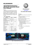
NCP1351LEDGEVB Universal Input, 20W, LED Ballast Evaluation Board User's Manual http://onsemi.com EVAL BOARD USER’S MANUAL Circuit Description In order to stay below IEC6100-3-2 Class C, the design has been optimized at < 25 W, so assuming 80% efficiency the maximum output power is ~20 W. The NCP1351 controller provides for a low cost, variable frequency, flyback converter. It incorporates a very low quiescent current allowing for high value resistors to be used as a start-up circuit direct from the HV rail. The design comprises and input filter, bridge rectifier (using low cost 1N4007 diodes), bulk capacitors and line inductor in p-filter arrangement, the power stage, rectifier diode and smoothing capacitors. Feedback is CVCC, constant current drive for the LED’s with a constant voltage in the event of an open circuit output. Key Features Wide Input Voltage Range – 85 Vac to 265 Vac Small Size, and Low Cost Good Line Regulation High Efficiency Overload and Short Circuit Protection Figure 1. NCP1351 Board Device Application Input Voltage Output Power Topology I/O Isolation NCP1351 Solid State Lighting 85−265 Vac 20 W Flyback Yes Table 1. OTHER SPECIFICATIONS Table 2. NUMBER OF LED’S IN SERIES Output 1 Maximum Output Voltage Ripple Nominal Curretn PFC (Yes/No) Target Efficiency Max Size 350 mA 700 mA 1A 1.5 A I 11 − * − III 10 6 4 * Rebel 10 6 4 * 33 V LUXEON Not Given LUXEON 700 mA LUXEON LUXEON K2 No 80% at Nominal Load 125 x 37 x 35 mm 11 6 4 2 Cree XLamp XR-E 12 8 5 * Cree XLamp XP-E 12 8 * * 12 7 5 * Operating Temp Range 0 to +70C OSRAM Platinum DRAGON Cooling Method/Supply Orientation Convection VZ (D10) 45 V 33 V 22 V 12 V R12 & R13 3R6 1R8 1R2 0R8 Signal Level Control No *Out of LED Specification Semiconductor Components Industries, LLC, 2012 February, 2012 − Rev. 3 1 Publication Order Number: EVBUM2059/D NCP1351LEDGEVB SCHEMATIC http://onsemi.com 2 NCP1351LEDGEVB LED Current designing, with a varying output voltage, we need the maximum output voltage. The light output of an LED is determined by the forward current so the control loop will be constant current, with a simple Zener to limit the maximum output voltage. Typical forward voltages vary by LED supplier, below are the nominal forward voltage characteristics of the LUXEON K2 at different operating currents. IF VF 350 mA 3.42 V 700 mA 3.60 V 1000 mA 3.72 V 1500 mA 3.85 V VIN(max) is the Maximum Rectified Input = 375 V VIN(min) is the Minimum Rectified Input = 80 V VOUT is 35 V (20 W @ 700 mA is 29 V plus a Margin for Safety) With a 600 V MOSFET and derating of 80%, our maximum allowable drain voltage is: V D(max) + 600 V CLAMP + V D(max) * V IN(max) + 480 * 375 + + 105 V kC + V CLAMP N ǒV OUT ) V fǓ + 1.5 (eq. 5) Vf = 0.7 V as we will need a High Voltage Diode Re-arranging for N: (eq. 1) Total sense resistor power dissipation is: 0.6 V (eq. 4) Good results are obtained if we set VCLAMP, at ~150% of the reflected secondary: The LED current is thus set by: P D + I LED (eq. 3) And thus headroom, VCLAMP for the reflected secondary voltage and leakage spike of: Driving eight LED’s at 700 mA thus gives an output power of 20.2 W at 28.8 V. The output current is sensed by a series resistance, once the voltage drop across this reaches the baseemitter threshold of the PNP transistor current flows in the opto-coupler diode and thus in the FB pin of the NCP1351. 0.6 V I LED + R SENSE 0.8 + 480 V N+ (eq. 2) NS 1.5 + NP (35 ) 0.7) + 0.51 105 (eq. 6) We will use a ratio of 0.5 or 2:1, this will give a good transformer construction. We can now calculate the maximum duty cycle running in CCM: So for 700 mA we need a 0.9 W sense resistor capable of dissipating 420 mW, two 330 mW surface mount resistors, 1.8 W each in parallel, are used. Inductor Selection d MAX + In a flyback converter the inductance required in the transformer primary is dependant on the mode of operation and the output power. Discontinuous operation requires lower inductance but results in higher peak to average current waveforms, and thus higher losses. For low power designs, such as this ballast, the inductance is designed to be just continuous (or just discontinuous) under worst case conditions, that is minimum line and maximum load. V OUT + V OUT ) V IN(min)N (35 ) 0.7) + + 0.47 (35 ) 7) ) 80 0.5 (eq. 7) The specification for this ballast is as follows: Universal Input – 85 Vac to 265 Vac 25 W Maximum Input Power – PFC Limit Assuming 80% Efficiency – 20 W Output Power 700 mA Output Current 100 kHz Operation at Full Load This gives us a minimum DC input voltage of 120 V, there will be some sag on the DC bulk capacitors so an allowance will be made for this by using 80 V as the minimum input voltage, including MOSFET drop etc. First we need to calculate the turn’s ratio, this is set by the MOSFET drain rating, line voltage and reflected secondary voltage. Since this is a constant current circuit we are Looking at the waveform of the current flowing in the primary of the inductor (above) if we define a term k equal to: k+ http://onsemi.com 3 DI L I1 (eq. 8) NCP1351LEDGEVB Rectifier Snubber And use the equation: L+ ǒVIN(min) d MAXǓ Testing demonstrated the need for snubbing on the rectifier as there was a large amount of ringing present after the rectifier turns off. The snubber consists of a resistor and capacitor in series, and knowing the junction capacitance and ringing frequency we can determine the necessary values: 2 (eq. 9) f SW kP IN Then we can determine the inductance we require. If k = 2 then we are in boundary conduction mode as the ripple current equals twice the average pulse current, so setting k to 2: Rs + 2 (80 0.47) L+ 100 10 3 2.0 25 + 283 mH (eq. 10) Thus we can now find the primary ripple current assuming operation in boundary conduction mode: + 80 0.47 10 *6 100 283 10 3 f+ (eq. 11) + 1.32 A P IN + 25 + 313 mA 80 V IN(min) I AVE + 0.313 + 662 mA 0.47 d max I RMS + I 1 Ǹd Ǹ ǒ Ǔ Thus: Ǹ0.47 I RMS + 0.665 + Rs + Ǔ 1.32 1)1 3 2 0.665 2 V DROP + 0.8 + 0.61 W 1.32 I PK + R SENSE + 0.526 2 0.61 ^ V SENSE 0.8 + ^ 3.0 kW I BIAS 270 10 *6 14.5 10 6) 2 + (eq. 22) Ǹ1.51 80 10 *6 + 137 W 10 *12 2 Ǹ1.51 p 10 *6 137 (eq. 23) 80 10 *12 + (eq. 24) Normally in a flyback converter the auxiliary winding would be in the form of a flyback winding, i.e. in phase with the output winding, and thus provide a semi-regulated voltage to supply the controller. As this ballast is current controlled and the output voltage can vary over a considerable range depending on the number of LED’s connected, a forward phased winding is used. The auxiliary will therefore vary with line rather than output voltage. Since neither option could supply sufficient volts at low input/output voltage whilst still staying below the maximum VCC figure of 28 V, a voltage regulator is used formed by Q1 and D6. Below ~20 V the regulator does nothing other than act as a small volt drop, however as the voltage rises it clamps the voltage to around 20.7 V, since the current is very low into the VCC pin there is very little loss. (eq. 17) Two 1.2 W resistors in parallel will be used as sub 1 W resistors typically cost more. The threshold voltage for the current sense is set by an offset resistor; this has a bias current of 270 mA in it so we can determine the resistor value: R OFFSET + (p Auxiliary Winding (eq. 16) ^ 170 mW 10 *12 The nearest standard values are 470 pF and 140 W, inserting these into the circuit eliminated the ringing due to the rectifier. (eq. 15) The total power dissipation is: 2 80 + 504 pF We can also determine the current sense resistor, allowing for a drop across the resistor of 0.8 V: P D(sense) + I RMS 1 4 Cs + + 526 mA R SENSE + 1 + 4C j(pf) 2 (eq. 14) ǒ (eq. 21) + 1.51 mH 2 Ǹ (eq. 20) Rs 1 2p ǸLC j L+ (eq. 13) Demonstrating that DIL does equal twice I1 and that the peak primary current is 1.32 A. We can calculate the RMS current in the MOSFET and sense resistor for dissipation purposes. For a stepped-sawtooth waveform of this type the equation is: DI L 1)1 3 2I 1 2p ǸLC j f = 14.5 MHz (Measured on Oscilloscope) Cj = 80 pF (Datasheet Figure for MUR840 at 62 V) (eq. 12) The average pulse current, I1, is: I1 + (eq. 19) We can determine L, the stray inductance which then allows us to calculate the necessary snubber resistor. The average input current, IAVE, is: I AVE + L Cj Knowing that: V IN(min) T ON V IN(min) d max + + L Lf SW DI L + Cs + Ǹ (eq. 18) http://onsemi.com 4 NCP1351LEDGEVB MAGNETICS DESIGN DATA SHEET Project/Customer: ON Semiconductor Part Description: 25 W Transformer Schematic ID: − Core Type: EE25 Core Gap: Gap for 250 mH Inductance: 250 mH Bobbin Type: NIC 10-Pin Vertical Windings (In Order): Winding # / Type Turns / Material / Gauge / Insulation Data N1, Primary Start on pin 1 and wind 20 turns, of 0.28 mm triple insulated wire (e.g. Tex-E), in one neat layer across the entire bobbin width. Finish on pin 2. N2, Secondary Start on pins 9&10 and wind 20 turns, of 0.8 mm Grade II ECW, distributed evenly across the entire bobbin width. Finish on pins 6&7. N3, Primary Start on pin 2 and wind 20 turns, of 0.28 mm triple insulated wire (e.g. Tex−E), in one neat layer across the entire bobbin width. Finish on pin 3. N4, Primary (Aux) Start on pin 4 and wind 5 turns, of 0.28 mm triple insulated wire, in one neat layer spread evenly across the entire bobbin width. Finish on pin 5. Sleeving and insulation between primary and secondary as required to meet the requirements of double insulation. Primary leakage inductance (pins 6&7 and 9&10 shorted together) to be < 6 mH. NIC part number: NLT282224W3P4020S5P10F Hipot: 3 kV between pins 1, 2, 3, 4 & 5 and pins 6, 7,8, 9 & 10 for 60 seconds. Schematic Lead Breakout / Pinout 1 5 N1 2 5 mm 6, 7 N2 N3 6 9, 10 3 4 N4 4 7 3 8 2 9 1 10 5 15 mm http://onsemi.com 5 NCP1351LEDGEVB Table 3. BILL OF MATERIALS Ref Part Type / Value Comment Footprint Description Manufacturer Part Number C1 220 nF X2 275 VAC 18 x 10 mm, 15 mm Pitch X-class EMI Suppression Capacitor NIC NPX224M275VX2MF C2 47 mF 400 V 16 mm, 7.5 mm Pitch General Purpose High Voltage Electrolytic NIC NRE−H470M400V16X31.5F C3 470 pF 100 V X7R 1206 Ceramic Chip Capacitor NIC NMC1206X7R471K100F C4 100 nF 50 V X7R 0603 Ceramic Chip Capacitor NIC NMC0603X7R104K50F C5 220 nF 50 V X7R 0805 Ceramic Chip Capacitor NIC NMC0805X7R224K50F C6 4.7 mF 35 V 5 mm, 2 mm Pitch General Purpose Low Voltage Electrolytic NIC NRWA4R7M50V5X11F C7 180 pF 50 V NP0 0603 Ceramic Chip Capacitor NIC NMC0603NPO181J50F C8 47 nF 50 V X7R 0603 Ceramic Chip Capacitor NIC NMC0603X7R473K50F C9 220 nF 50 V X7R 0805 Ceramic Chip Capacitor NIC NMC0805X7R224K50F C10 10 nF (0.01 mF) 1 kV 1210 Ceramic Chip Capacitor JOHANSON C11 1 mF 50 V 5 mm, 2 mm Pitch General Purpose Low Voltage Electrolytic Ceramic Y-class Capacitor 102S41W103KV4E NIC NRWA1R0M50V5X11F Murata DE1E3KX102MN4AL01 C12 1 nF Y1 Radial, Pitch 10 mm C13 470 mF 63 V 12.5 mm, 5 mm Pitch C14 Not Inserted − − C15 220 nF 100V X7R 1206 Ceramic Chip Capacitor NIC NMC1206X7R224K100F C16 1 mF 50 V 1206 Ceramic Chip Capacitor NIC NMC1206X7R105K50F D1 1N4007 1 A, 1000 V Axial Axial Lead, Standard Recovery ON Semiconductor 1N4007RLG D2 1N4007 1 A, 1000 V Axial Axial Lead, Standard Recovery ON Semiconductor 1N4007RLG D3 1N4007 1 A, 1000 V Axial Axial Lead, Standard Recovery ON Semiconductor 1N4007RLG Axial Lead, Standard Recovery ON Semiconductor 1N4007RLG Switching Diode ON Semiconductor MMSD4148T1G D4 1N4007 1 A, 1000 V Axial D5 MMSD4148 200 mA, 100 V SOD−123 Miniature Low Impedance Electrolytic − NIC − NRSZ471M63V12.5X25F − D6 20 V 1.5 W SMA Zener Diode ON Semiconductor 1SMA5932BT3G D7 MURA160 1 A, 600 V SMA Ultrafast Rectifier ON Semiconductor MURA160T3G D8 MMSD4148 200 mA, 100 V SOD−123 Switching Diode ON Semiconductor MMSD4148T1G D9 MUR840 (MUR860 - Alt) 8 A, 400 V TO−220 Ultrafast Power Rectifier ON Semiconductor MUR840G D10 33 V 5%, 200 mW SOD323 Zener Diode ON Semiconductor MM3Z33VT1G IC1 NCP1351B − SOIC8 Variable Off-time PWM Controller ON Semiconductor NCP1351BDR2G IC2 HCPL−817 Wide Pitch HCPL−817−300E Agilent HCPL−817−W0AE Opto-coupler HCPL−817 L1 − − WE−LF 662/SH AC 2-Way 5 mm Pitch − Common Mode Choke Screw Terminal Keystone 8718 LED 2-Way 5 mm Pitch − Screw Terminal Phoenix 1985881 M1 25.9C/W − − Heatsink Aavid 577102B00000G M2 25.9C/W − − Heatsink Aavid 577102B00000G Q1 BC847 45 V SOT−23 General Purpose NPN Q2 IRFBC40A 600 V TO−220 MOSFET Q3 BC857 −45 V SOT−23 General Purpose PNP R1 150R 0.33 W, 5% 1210 R2 2k2 0.1 W, 5% 0603 Wurth/Midcom ON Semiconductor IR 744 662 0027 BC847ALT1G IRFBC40A ON Semiconductor BC857ALT1G Resistor Thick Film NRC NIC NRC25J151F Resistor Thick Film NRC NIC NRC06J222F R3 3k0 0.1 W, 5% 0603 Resistor Thick Film NRC NIC NRC06J302F R4a 1R2 1 W, 5% 2512 Resistor Thick Film NRC NIC NRC100J1R2F R4b 1R2 1 W, 5% 2512 Resistor Thick Film NRC NIC NRC100J1R2F R5 1M 0.5 W, 5% Axial Metal Film Resistor http://onsemi.com 6 Vishay SFR2500001004J−R500 NCP1351LEDGEVB Table 3. BILL OF MATERIALS Ref Part Type / Value Comment Footprint Description Manufacturer R6 1M 0.5 W, 5% Axial Metal Film Resistor R7 2k2 0.125 W, 5% 0805 Resistor Thick Film NRC NIC NRC10J222BF R8 10R 0.25 W, 5% 1206 Resistor Thick Film NRC NIC NRC12J100F R9 6k8 0.1 W, 5% 0603 Resistor Thick Film NRC NIC NRC06J682TRF Vishay Part Number SFR2500001004J−R500 R10 12k 2 W, 5% Axial Carbon Film Resistor NIC NCF200J123TRF R11 200R 0.125 W, 5% 0805 Resistor Thick Film NRC NIC NRC10J201F R12 1R8 0.33 W, 1% 1210 Resistor Thick Film NRC NIC NRC25J1R8F R13 1R8 0.33 W, 1% 1210 Resistor Thick Film NRC NIC NRC25J1R8F R14 2K2 0.125 W, 5% 0805 Resistor Thick Film NRC NIC NRC10J222BF R15 4k3 0.125 W, 5% 0805 Resistor Thick Film NRC NIC NRC10J432F R16 0 W Short 0.125 W 0805 Resistor Thick Film Chip Vishay Tx1 25 W LED Transformer − NIC 10 Pin Vertical 25 W Flyback Transformer COMPONENT PLACEMENT AND PCB LAYOUT Figure 2. Top View Figure 3. Bottom View http://onsemi.com 7 NIC CRCW08050000Z0EA NLT282224W3P4020S5P10F NCP1351LEDGEVB TYPICAL OPERATIONAL RESULTS Figure 4. Drain Waveform at 120 Vac and 230 Vac Figure 5. Turn-off in Detail at 120 Vac, 230 Vac and 265 Vac http://onsemi.com 8 NCP1351LEDGEVB TYPICAL EVALUATION RESULTS 90% 80% 70% Efficiency (%) 60% 50% 40% 30% 115 Vac 230 Vac 20% 10% 0% 0 5 10 15 20 25 30 LED Voltage (Vdc) Figure 6. Efficiency vs. Line and Load @ 700 mA Ta = 215C/705F 0.8 0.7 LED Current (A) 0.6 0.5 0.4 230 Vac 0.3 115 Vac 0.2 0.1 0.0 0 3.5 7 10.5 14 17.5 21 24.5 LED Forward Voltage (Vdc) Figure 7. Current Regulation vs. Forward Voltage @ 700 mA Ta = 215C/705F http://onsemi.com 9 28 31.5 35 NCP1351LEDGEVB Modifying the Board for Other LED Currents the maximum voltage capability increases. For example, for 20 W output, the maximum voltage at 350 mA could be as high as 57 Vdc. Under UL1310, Class 2 power supplies for use in dry/damp environments are allowed to have a maximum output voltage of 60 Vdc. On the demo board, Q3 is implemented using a BC857 transistor which has a maximum VCEO of −45 Vdc. If a higher operating voltage is required, this transistor can be changed to a BC856 (maximum VCEO of −65 Vdc). The figure below shows the current regulation performance for a nominal 350 mA output current with the component changes as noted. The constant current constant voltage secondary control loop is very flexible and is implemented using a PNP (Q3) with a pair of current sense resistors (R12 & R13) to regulate the current and provide control of the optocoupler to the NCP1351. In addition, there is a maximum voltage control loop that is implemented using zener D10. To modify this circuit for alternate current/voltage configurations, these components should be modified. The table on the front page shows several other possible configuration options. Note because this design is ultimately power limited based on the transformer design and FET used, as the current decreases, R12 & R13 = 3.6 W each, D10 = MMSZ5263B (56 V), Q3 = BC856 0.40 0.35 LED Current (A) 0.30 0.25 0.20 0.15 0.10 0.05 0.00 0 5 10 15 20 25 30 35 40 45 50 55 60 LED Forward Voltage (Vdc) Figure 8. Typical Current Regulation vs. Load, Ta = 215C/705F LUXEON is a registered trademark of Philips Lumileds Lighting Company and Royal Philips Electronics of the Netherlands. Platinum DRAGON LED is a registered trademark of OSRAM Opto Semiconductors, Inc. XLamp is a registered trademark of Cree, Inc. ON Semiconductor and are registered trademarks of Semiconductor Components Industries, LLC (SCILLC). SCILLC reserves the right to make changes without further notice to any products herein. SCILLC makes no warranty, representation or guarantee regarding the suitability of its products for any particular purpose, nor does SCILLC assume any liability arising out of the application or use of any product or circuit, and specifically disclaims any and all liability, including without limitation special, consequential or incidental damages. “Typical” parameters which may be provided in SCILLC data sheets and/or specifications can and do vary in different applications and actual performance may vary over time. All operating parameters, including “Typicals” must be validated for each customer application by customer’s technical experts. SCILLC does not convey any license under its patent rights nor the rights of others. SCILLC products are not designed, intended, or authorized for use as components in systems intended for surgical implant into the body, or other applications intended to support or sustain life, or for any other application in which the failure of the SCILLC product could create a situation where personal injury or death may occur. Should Buyer purchase or use SCILLC products for any such unintended or unauthorized application, Buyer shall indemnify and hold SCILLC and its officers, employees, subsidiaries, affiliates, and distributors harmless against all claims, costs, damages, and expenses, and reasonable attorney fees arising out of, directly or indirectly, any claim of personal injury or death associated with such unintended or unauthorized use, even if such claim alleges that SCILLC was negligent regarding the design or manufacture of the part. SCILLC is an Equal Opportunity/Affirmative Action Employer. This literature is subject to all applicable copyright laws and is not for resale in any manner. PUBLICATION ORDERING INFORMATION LITERATURE FULFILLMENT: Literature Distribution Center for ON Semiconductor P.O. Box 5163, Denver, Colorado 80217 USA Phone: 303−675−2175 or 800−344−3860 Toll Free USA/Canada Fax: 303−675−2176 or 800−344−3867 Toll Free USA/Canada Email: [email protected] N. American Technical Support: 800−282−9855 Toll Free USA/Canada Europe, Middle East and Africa Technical Support: Phone: 421 33 790 2910 Japan Customer Focus Center Phone: 81−3−5817−1050 http://onsemi.com 10 ON Semiconductor Website: www.onsemi.com Order Literature: http://www.onsemi.com/orderlit For additional information, please contact your local Sales Representative EVBUM2059/D