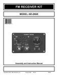
1
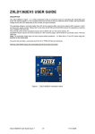
ZXLD1350EV2
ZXLD1350EV2 EVALUATION BOARD USER GUIDE
DESCRIPTION
The ZXLD1350EV2, Figure 1, is an evaluation board for evaluating the ZXLD1350 350mA LED driver with internal
switch. The evaluation board can be used to drive 1, 2 or 3 one-watt LEDs, or an external choice of LEDs. The
number of external connected LEDs depends on the forward voltage of the LEDs connected. A connector, J1, is
provided, which is compatible with the modular evaluation system used by Future Electronics Ltd. The LEDs fitted on
this evaluation board are from the LUXEON ® range distributed by Future Lighting Solutions
(www.FutureLightingSolutions.com)
The operating voltage is nominally 24V. For three 1W series-connected LEDs, the voltage can be from 12V minimum
to 30V maximum. The 100uH inductor used in the circuit is based on a nominal 24V supply, which should be
connected across +VIN and GND pins. Note: The evaluation board does not have reverse battery protection. The
nominal current for the evaluation board is set at 300mA with a 0.33Ω sense resistor, Rs.
Jumpers J1, J2 and J3 allow the selection of the number of LEDs to be connected in series. Jumper on at J1
bypasses LED D1. Jumper on at J3 bypasses LED D3. Removing jumper J2 disconnects all the on-board LEDs from
the current flow path. Jumper 2 also doubles as a connection point for an ammeter to measure the LED current.
Before connecting external LEDs across test pins LED+ and LED-, or across J1, remove jumper J2. Jumpers J1 and
J2 can be on or off.
Test point ADJ provides a connection point for DC or PWM dimming and shutdown.
Warning: At 24V nominal operation with 300mA output, the LEDs and the PCB may be hot and the LEDs will be very
bright.
Figure 1: ZXLD1350EV2 evaluation board
ZXLD1350EV2 User Guide Iss 5
10-04-07
ZXLD1350EV2
ZXLD1350 DEVICE DESCRIPTION
The ZXLD1350 is a continuous mode inductive driver in a TSOT23-5 package, for driving one or more series
connected LEDs efficiently from a voltage source higher than the LED voltage. The device includes the output
switch and a current sense circuit, which requires an external sense resistor to set the nominal current up to
350mA.
ZXLD1350 DEVICE FEATURES
•
Drives one or more series-connected 1W white
LEDs up to 350mA.
•
Internal 30V switch.
•
Wide input voltage: 7V to 30V.
•
Inherent open circuit LED protection.
•
Brightness control using DC or PWM.
•
Internal PWM filter.
DEVICE APPLICATIONS
•
LED flashlights.
•
High Power LED driving.
•
Low-voltage halogen replacement LEDs.
•
Automotive lighting.
•
Illuminated signs.
ZXLD1350 Device Packages, Pin and Definitions
TSOT23-5 pack
ZXLD1350 Device Pin Definition
Name
Pin No
LX
1
GND
2
ADJ
3
ISENSE
4
VIN
5
Description
Drain of NDMOS switch.
Ground (0V).
Internal voltage ref. pin (1.25V) :
•
Leave floating for normal operation.
•
Connect to GND to turn off output current.
•
Drive with DC voltage (0.3V to 1.25V) or with PWM signal to adjust
output current or....
•
Connect a capacitor from this pin to ground to set soft-start time.
Connect a sense resistor, Rs, from the ADJ pin to VIN to sense the nominal
output current. Nominal Iout = 0.1/ Rs
Input voltage: 7V to 30V. Decouple to ground with a 1uF or higher ceramic
capacitor.
ORDERING INFORMATION
EVALBOARD ORDER NUMBER
ZXLD1350EV2
DEVICE ORDER NUMBER
ZXLD1350E5TA
Please note: Evaluation boards are subject to
availability and qualified leads.
ZXLD1350EV2 User Guide Iss 5
10-04-07
ZXLD1350EV2
ZXLD1350EV2 EVALUATION BOARD
REFERENCE DESIGN
The ZXLD1350EV2 is configured to the reference design in Figure 2. The target application is a driver for one or
more series-connected 1W white LEDs for torches and other high powered LED driving applications.
The operating voltage is a nominal 24V. For three 1W series-connected LEDs, the voltage can be from 12V
minimum to 30V maximum. The nominal current is set at 300mA with a 0.33Ω sense resistor, Rs. For three series connected 1–watt LEDs, with a nominal supply of 24V, the ZXLD1350 runs in continuous mode at 545kHz, with a
100uH inductor.
Jumpers J1, J2 and J3 allow selection of the number of LEDs to be connected in series. Jumper on at J1 bypasses
LED D1. Jumper on at J3 bypasses LED D3. Removing jumper J2 disconnects all the 1-watt LEDs from the current
flow path. Jumper 2 also doubles as a connection point for an ammeter to measure the LED current.
Both DC and PWM dimming can be achieved by driving the ADJ pin. For DC dimming, the ADJ pin may be driven
between 0.3V and 1.25V. Driving the ADJ pin below 0.2V will shutdown the output current. For PWM dimming, an
external open-collector NPN transistor or open-drain N-channel MOSFET can be used to drive the ADJ pin. The
PWM frequency can be low, around 100Hz to 1kHz, or high between 10kHz to 50kHz. C3 should not be fitted on the
evaluation board when using the PWM dimming feature. Shorting R1 will connect the test pin ADJ to device pin ADJ.
The capacitor C3 should be around 10nF to decouple high frequency noise at the ADJ pin for DC dimming.
The soft-start time will be nominally 0.5ms without capacitor C3. Adding C3 will increase the soft start time by
approximately 0.5ms/nF
For other reference designs or further applications information, please refer to the ZXLD1350 datasheet.
Schematic Diagram
Figure 2 shows the schematic for the ZXLD1350EV2 evaluation board.
Figure 2: Schematic for the evaluation board ZXLD1350EV2
ZXLD1350 Operation
In normal operation, when voltage is applied at +VIN, the ZXLD13350 internal NDMOS switch is turned on. Current
starts to flow through sense resistor Rs, inductor L1, and the LEDs. The current ramps up linearly, and the ramp rate
is determined by the input voltage +VIN and the inductor L1. This rising current produces a voltage ramp across Rs.
The internal circuit of the ZXLD1350 senses the voltage across Rs and applies a proportional voltage to the input of
the internal comparator. When this voltage reaches an internally set upper threshold, the NDMOS switch is turned off.
The inductor current continues to flow through Rs, L1, the LEDs, the schottky diode SD1, and back to the supply rail,
but it decays, with the rate of decay determined by the forward voltage drop of the LEDs and the schottky diode. This
decaying current produces a falling voltage at Rs, which is sensed by the ZXLD1350. A voltage proportional to the
sense voltage across Rs is applied at the input of the internal comparator. When this voltage falls to the internally set
lower threshold, the NDMOS switch is turned on again. This switch-on-and-off cycle continues to provide the average
LED current set by the sense resistor Rs. Please refer to the datasheets for the threshold limits, ZXLD1350 internal
circuits, electrical characteristics and parameters.
ZXLD1350EV2 User Guide Iss 5
10-04-07
ZXLD1350EV2
ZXLD1350EV2 Evaluation Board.
Ref
Value
Package
Part Number
Manufacturer
RS
0805
NCST10FR330FTRF
NIC
components
R1,R2
C1,C2
0.33R
1%,200ppm
Not fitted
1uF, 50V
50V, 1206 X7R
NMC1206X7R105K50F
NIC
components
C3
L1
Not fitted
100uH
0805
NPIS53D101MTRF
SD1
U1
D1, D2, D3
JP1, JP2,
JP3
+VIN, GND,
ADJ, LED a,
LED k
J1
40V, 1.16A
ZXLD1350
1W LED
Jumper
SOT23
TSOT23-5
NIC
components
Zetex
Zetex
Lumileds
Various
0805
1206
Notes
Not fitted
ZLLS1000
ZXLD1350E5TA
LXHL-PW01
Test loop
100-108
Hughes
6 way
connector
5535676-5
TYCO
Not fitted
100uH/0.5A rms
Inductor
Schottky diode
DC-DC converter
1W power LED
2.54mm pitch
jumper pin strips
The slugs of the 1-watt LEDs are connected to isolated copper 'floods' both on the top and bottom layers, with
thermal inter-connection between the layers. The slugs are electrically isolated from other circuits and pads on the
evaluation board. Warning: At a nominal 24V operation with 300mA output, the board temperature rises by
around 30C from ambient after 30 minutes of operation.
ZXLD1350EV2
EVALUATION BOARD
k
D1
LED k
a
JP1
JP2
C2
k
+VIN
R2
L1
C3
J1
D2
U1
SD1
GND
C1
a
RS
1
R1
ADJ
JP3
k
In partnership with:
LED a
D3
Bare board: ZDB308R3
Copyright Zetex Plc 2006
a
Figure 3: Component layout
ZXLD1350EV2 User Guide Iss 5
10-04-07
ZXLD1350EV2
ZXLD1350EV2
EVALUATION BOARD
k
D1
LED k
a
JP1
JP2
C2
R2
L1
C3
J1
k
+VIN
D2
U1
SD1
GND
C1
a
RS
1
R1
ADJ
JP3
k
In partnership with:
LED a
D3
Bare board: ZDB308R3
Copyright Zetex Plc 2006
a
Figure 4: Top View
Figure 5: Bottom View
ZXLD1350EV2 Connection Point Definition
Name
Description
+VIN
Positive supply voltage. Connect a +24V positive supply to this pin.
GND
Supply Ground (0V). Connect supply ground to this pin.
ADJ
LED a
LED k
J1
Internal voltage ref. pin (1.25). This pin can be used to achieve dimming and soft-start,
and for switching the output current off.
•
Leave floating for normal operation.
•
See 'Other Features' section to achieve dimming, and soft-start and for switching
the output current off.
LED a connects to the ANODE of LED D3, and is the external LED anode connection
point. Disconnect the jumper JP2 when driving an external load.
LED k connects to the CATHODE of LED D1, and is the external LED cathode
connection point. Disconnect the jumper JP2 when driving external LEDs.
Pins 1 & 2: LED a, Pins 5 & 6: LED k
ZXDL1350EV2 OPERATION
ZXLD1350EV2 Power Up
1.
2.
3.
4.
5.
Connect VIN to +24V of the power supply unit (PSU). Connect GND to the power supply ground (0V).
Warning: The board does not feature reverse battery/supply protection.
Set the PSU to +24V. (+24V at VIN pin with ref. to the GND pin.)
Turn on the PSU.
Warning: Do not stare at the LEDs directly.
Ensure jumper J2 is fitted. With JP1 and JP3 disconnected (jumper off), all three LEDs should illuminate and
will be regulated nominally at 300mA.
To change the number of LEDs connected in series, use jumper JP1 and JP3 to bypass LEDs D1 and D3
respectively.
Warning: The LEDs may be hot.
ZXLD1350EV2 User Guide Iss 5
10-04-07
ZXLD1350EV2
OTHER FEATURES
Dimming
The ZXLD1350 provides three dimming options: DC, high-frequency PWM, and low-frequency PWM dimming.
DC Voltage Dimming
1. Switch off the power supply.
2. Solder a link across R1 pads.
3. Fit a 10nF capacitor at C3 to decouple the pin.
4. Drive the ADJ pin on the board with a DC voltage in the range 0.3V to 1.25V.
5. Do not exceed 1.25V, as this represents 100% of the LED current set by Rs. The current will increase in
proportion to this voltage. For example, if 2.5V is applied, the current will increase to 200%. That is, the
current will be twice the 1.25V rating. For such over-drive of the ADJ pin, the LED and ZXLD1350 are likely
to be damaged. The nominal LED current (output current), IOUT, is given by
IOUT = 0.08* VADJ/Rs
6.
7.
where
IOUT = the nominal LED current.
VADJ = the DC dimming voltage at ADJ pin resistor.
0.08 is the multiplier for the reference voltage on ADJ pin.
Rs = the sense resistor value in ohms.
Do not use a resistor value lower than 0.27Ω.
The dimming ratio is around 6:1. Note: as the voltage approaches 0.2V on the ADJ pin, the ZXLD1350 will
shut down.
Follow the ‘ZXLD1350EV2 Power Up’ sequence.
High Frequency PWM Dimming
1.
2.
3.
4.
5.
6.
7.
Switch off the power supply.
Solder a link across R1 pads.
Ensure C3 is not fitted.
Connect a PWM signal to the ADJ pin via an open collector NPN transistor, or an open drain N-channel
MOSFET.
Alternatively, drive the ADJ pin directly with a PWM signal. However, make sure the PWM signal voltage
levels do not violate the ADJ pin voltage rating. Driving the ADJ pin above 1.25V will exceed the maximum
set current for the value of Rs and may damage the device or LED.
Set the PWM frequency to between 10KHz and 50KHz. The cut-off frequency of the internal filter is 4kHz,
and exceeding the 50kHz may cause modulation with the switching regulator.
The dimming ratio will be about 6:1, similar to the DC dimming. The nominal LED current (output current),
IOUT, is given by
IOUT = 0.1*D/Rs
8.
where
IOUT = the nominal LED current.
Rs = the sense resistor value in ohms.
Do not use a resistor value lower than 0.27Ω.
D = the duty cycle of the PWM dimming frequency.
0.1V is the nominal sense voltage with ADJ open circuit or set to 1.25V.
Note: The ADJ pin is internally referenced to 1.25V. This pin should be left floating for normal operation
without dimming. Please refer to the datasheet for PWM frequency.
Follow the ‘ZXLD1350EV2 Power Up’ sequence.
ZXLD1350EV2 User Guide Iss 5
10-04-07
ZXLD1350EV2
Low Frequency PWM Dimming
1.
2.
3.
4.
5.
6.
7.
Switch off the power supply.
Solder a link across R1 pads.
Make sure C3 is not fitted.
Connect a PWM signal to the ADJ pin via an open collector NPN transistor or an open drain N-channel
MOSFET.
Alternatively, drive the ADJ pin directly with a PWM signal. However, make sure the PWM signal voltage
levels do not violate the ADJ pin voltage rating. Driving the ADJ pin above 1.25V will exceed the maximum
set current for the value of Rs and may damage the device or LED
The PWM frequency can be low; around 100Hz or up to 1kHz.
The ZXLD1350 is now effectively being turned on and off at the PWM frequency. The dimming ratios are in
the region of 100:1, much greater than the DC dimming ratio. The average l LED current (output current),
IOUT, is given by
IOUT = 0.1*D/Rs
8.
where
IOUT = the average LED current.
Rs = the sense resistor value in ohms.
Do not use a resistor value lower than 0.27Ω.
D = the duty cycle of the PWM dimming frequency.
0.1V is the nominal sense voltage with ADJ open circuit or set to 1.25V.
Follow the ‘ZXLD1350EV2 Power Up’ sequence.
Soft-start
1.
2.
3.
4.
Switch off the power supply.
Solder a link across R1 pads.
Fit a capacitor at C3 to decouple the pin. The value of C3 will determine the soft-start time setting. Please
see the datasheet for calculation of the capacitor value.
Follow the ‘ZXLD1350EV2 Power Up’ sequence.
Switching the output current off
1.
2.
3.
4.
5.
Switch off the power supply.
Solder a link across R1 pads.
Follow the ‘ZXLD1350EV2 Power Up’ sequence.
Connect the ADJ pin to GND to turn off the output current.
Follow the ‘ZXLD1350EV2 Power Up’ sequence. The ZXLD1350 internal switch remains switched off (output
current off) whilst the ADJ pin is pulled to GND.
Changing the LED current
1.
2.
3.
Switch off the power supply.
Remove Rs.
Calculate and fit a new sense resistor, Rs, the value of which is based on the required LED current without
dimming. Rs can be calculated using following equation :
Rs = 0.1V/IOUT
4.
where
IOUT = the LED current.
Rs = the sense resistor value in ohms.
Do not use a resistor value lower than 0.27Ω.
0.1V is the nominal sense voltage with ADJ open circuit or set to 1.25V.
Follow the ‘ZXLD1350EV2 Power Up’ sequence.
Using external LEDs or loads
1.
2.
3.
Switch off the power supply.
Connect external LEDs across test pins ‘LED a’ and ‘LED k’. ‘LED a’ is the LEDs' anode connection point
and ‘LED k’ is the LEDs' cathode connection point. The number of external LEDs that can be connected
depends on their operating power and forward voltage drop. For an external load other than LEDs, the
positive terminal of the load should be connected to test pin ‘LED a’ and the negative terminal of the load
should be connected to test pin ‘LED k’. Connector J1 is compatible with the ‘Luxeon® Emitter Board
System’ from Future Electronics, or can be used to connect LEDs via pin-strip connectors.
Follow the ‘ZXLD1350EV2 Power Up’ sequence.
ZXLD1350EV2 User Guide Iss 5
10-04-07
ZXLD1350EV2
PERFORMANCE
The system efficiency depends on the sense resistor, supply voltage, switching inductor and the number of 1W LEDs
connected in series.
The graph below shows the efficiency with a 0.33Ω sense resistor RS, and a 100uH inductor, for 1 to 3 series
connected 1W LEDs.
With a 24V supply, the switching frequency is typically 545kHz for three series-connected 1-watt LEDs and 300kHz
for a single 1-watt LED.
With a 12V supply, the switching frequency is typically 160kHz for three series-connected 1-watt LEDs and 280kHz
for a single 1-watt LED
The detailed performance information for the device can be found in the datasheets.
Efficiency vs Vin
Rsense=0.33 Ohms, L=100uH (NIC NPIS53D101MTRF)
95
90
Eff (%)
1 LED
85
2 LED
3 LED
80
75
0
5
10
15
20
25
30
35
Vin (V)
Figure 6: Efficiency vs supply voltage
ZXLD1350EV2 User Guide Iss 5
10-04-07
ZXLD1350EV2
Definitions
Product change
Zetex Semiconductors reserves the right to alter, without notice, specifications, design, price or conditions of supply of any product or service.
Customers are solely responsible for obtaining the latest relevant information before placing orders.
Applications disclaimer
The circuits in this design/application note are offered as design ideas. It is the responsibility of the user to ensure that the circuit is fit for the user’s
application and meets with the user’s requirements. No representation or warranty is given and no liability whatsoever is assumed by Zetex with
respect to the accuracy or use of such information, or infringement of patents or other intellectual property rights arising from such use or otherwise.
Zetex does not assume any legal responsibility or will not be held legally liable (whether in contract, tort (including negligence), breach of statutory
duty, restriction or otherwise) for any damages, loss of profit, business, contract, opportunity or consequential loss in the use of these circuit
applications, under any circumstances.
Life support
Zetex products are specifically not authorized for use as critical components in life support devices or systems without the express written approval of
the Chief Executive Officer of Zetex Semiconductors plc. As used herein:
A.
Life support devices or systems are devices or systems which:
1. are intended to implant into the body
or
2. support or sustain life and whose failure to perform when properly used in accordance with instructions
for use provided in the labeling can be reasonably expected to result in significant injury to the user.
B.
A critical component is any component in a life support device or system whose failure to perform can be reasonably expected to cause the
failure of the life support device or to affect its safety or effectiveness.
Reproduction
The product specifications contained in this publication are issued to provide outline information only which (unless agreed by the company in writing)
may not be used, applied or reproduced for any purpose or form part of any order or contract or be regarded as a representation relating to the
products or services concerned.
Terms and Conditions
All products are sold subjects to Zetex’ terms and conditions of sale, and this disclaimer (save in the event of a conflict between the two when the
terms of the contract shall prevail) according to region, supplied at the time of order acknowledgement.
For the latest information on technology, delivery terms and conditions and prices, please contact your nearest Zetex sales office.
Quality of product
Zetex is an ISO 9001 and TS16949 certified semiconductor manufacturer.
To ensure quality of service and products we strongly advise the purchase of parts directly from Zetex Semiconductors or one of our regionally
authorized distributors. For a complete listing of authorized distributors please visit: www.zetex.com/salesnetwork
Zetex Semiconductors does not warrant or accept any liability whatsoever in respect of any parts purchased through unauthorized sales channels.
ESD (Electrostatic discharge)
Semiconductor devices are susceptible to damage by ESD. Suitable precautions should be taken when handling and transporting devices. The
possible damage to devices depends on the circumstances of the handling and transporting, and the nature of the device. The extent of damage can
vary from immediate functional or parametric malfunction to degradation of function or performance in use over time. Devices suspected of being
affected should be replaced.
Green compliance
Zetex Semiconductors is committed to environmental excellence in all aspects of its operations which includes meeting or exceeding regulatory
requirements with respect to the use of hazardous substances. Numerous successful programs have been implemented to reduce the use of
hazardous substances and/or emissions.
All Zetex components are compliant with the RoHS directive, and through this it is supporting its customers in their compliance with WEEE and ELV
directives.
Product status key:
“Preview”
“Active”
“Last time buy (LTB)”
“Not recommended for new designs”
“Obsolete”
Datasheet status key:
“Draft version”
“Provisional version”
“Issue”
Future device intended for production at some point. Samples may be available
Product status recommended for new designs
Device will be discontinued and last time buy period and delivery is in effect
Device is still in production to support existing designs and production
Production has been discontinued
This term denotes a very early datasheet version and contains highly provisional
information, which may change in any manner without notice.
This term denotes a pre-release datasheet. It provides a clear indication of anticipated performance. However,
changes to the test conditions and specifications may occur, at any time and without notice.
This term denotes an issued datasheet containing finalized specifications. However, changes to specifications
may occur, at any time and without notice.
Europe
Americas
Asia Pacific
Corporate Headquarters
Zetex GmbH
Kustermann-park
Balanstraße 59
D-81541 München
Germany
Telefon: (49) 89 45 49 49 0
Fax: (49) 89 45 49 49 49
[email protected]
Zetex Inc
700 Veterans Memorial Highway
Hauppauge, NY 11788
USA
Zetex (Asia Ltd)
3701-04 Metroplaza Tower 1
Hing Fong Road, Kwai Fong
Hong Kong
Zetex Semiconductors plc
Zetex Technology Park, Chadderton
Oldham, OL9 9LL
United Kingdom
Telephone: (1) 631 360 2222
Fax: (1) 631 360 8222
[email protected]
Telephone: (852) 26100 611
Fax: (852) 24250 494
[email protected]
Telephone (44) 161 622 4444
Fax: (44) 161 622 4446
[email protected]
ZXLD1350EV2 User Guide Iss 5
10-04-07