1
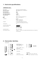
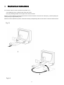
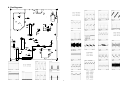
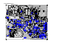
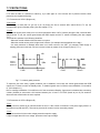
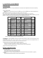
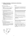
SERVICE MANUAL
CHASSIS CTU-AA
1. Technical specifications
CHASSIS CTU - AA
Mains voltage
Power cons. at 220V~
Aerial input impedance
Min. aerial input VHF
Min. aerial input UHF
Max. aerial input VHF/UHF
Pull-in range colour sync.
Pull-in range horizontal sync.
Pull-in range vertical sync.
Picture tube range
: 220 - 240 V ± 10% AC; 50 Hz (±5%)
: 35 W (14’’), 50W (20’’/21’’), 3W (Stand-By)
: 75 Ω - coax
: 30µV
: 40µV
: 180mV
: ± 300Hz
: ± 600 Hz
: ± 5 Hz
: 14'' / 20’’ / 21‘’
: Mono: 25∧ 1W (14’’), 16∧ 2W (20’’/21’’)
: Stereo : 2x16∧ 2x4W (21’’)+
TV Systems
:
:
:
:
PAL BG
PAL I
PAL BG / SECAM BG DK
PAL BG I / SECAM BG L L'
Indications
: On screen display (OSD) green and menu
: 1 LED (red in ON and blinking red in stand-by)
VCR programs
: 99
Tuning and operating system
:
UV1315A / IEC (VST)
: VHFa: 48 - 168 MHz
: VHFb: 175 - 447 MHz
: UHF: 455 - 855 MHz
U1343A / IEC (VST)
: UHF: 455 - 855 MHz
Local operating functions
: Vol/Prog, +, -, contrast, colour, brightness and sharpness (and hue on program AV
with NTSC signal).
VST
2. Connection facilities
Euroconector:
1
2
3
4
5
6
7
8
9
10
-
Audio
Audio
Audio
Audio
Blue
Audio
Blue
CVBS status 1
Green
11 - Green
12
13
14
15
-
Red
Red
16 - RGB status
R (0V5 RMS ó 1K ).
R (0V2 - 2V RMS ò 10K ).
L ( 0V5 RMS ó 1K ).
17
18
19
20
21
-
CVBS
CVBS
CVBS
CVBS
( 1Vpp 75W ).
( 1Vpp/75W ).
Earthscreen.
L (0V2 - 2V RMS ò 10K ).
(0V7pp/75W ).
(0-2V int., 10-12V ext.).
(0V7pp/75W ).
Head phone:
(0V7pp/75W ).
8 to 600Ω. Mono : 25mW at 32Ω
(0-V4 int.) (1-3V ext. 75W ).
Stereo : 2x 6mW at 32Ω. 3,5mm ø.
3
3. Mechanical instructions
For the main carrier two service positions are possible (3.1).
A: For faultfinding on the component side of the main carrier.
B: For (de) soldering activities on the copper side of the main carrier.
Position A can be reached by first removing the mains cord from it's fixation, then loosen the carrier lips (1) and then pulling the
carrier panel (2) for approximately 10cm.
Position B can be reached from position A after disconnecting the degaussing cable. Put the carrier on the line transformer side.
Fig. 3.1
Fig. 3.2
4
4. Oscillograms
5
5. Print Board Layout
UHF
+8
3004
2K7
+8
3006
2K7
SC_AUDIOOUT
V_VARI
9103
A1
2092
RES
3010 *
3007*
100R
*
3026*
100R
2091
RES
3
3003*
100R
2090
RES
3002
2K7
VHFI
C11
A1
A7
13V
15K
2610
220N
3610 *
2602
10U
*
4
+5A
9496
2K7
9416
2001
100U
7104 *
BC847
+8
3008
4K7
5K6
3104 *
3103
1K2
2006
22N
1
6
2416
100N
2
2412
2N2
2411
2N2
2417
TP11 100N
+12B
9414
+45
9664
9665
7605 *
PMBT2369
3410 *
3613
47K
3614
47K
270R
3663
150
3605
220K
3412
2K
1%
5
*
3604 *
3603
24K
3411
2K
1%
3416
3415
3615
RES
3675
1K3
6413 *
2403
68N
-TUNER - 1001
330K
3413 *
VHFIII
A5
+8
A8
TP15
3402
390R
- FRAME -
M5:2
TP16
9417
VGUARD
VHFIII
UHF
VHFI
LED
VHFIII
INT/EXT
MUTE
3414
75R
10K
7601 *
BC847
3611*
10K
2611
220N
6602
HZT33
*
3602
1K5
3612
KEYBOARD
V_VARI
M5:1
A9
A5
A8
A7
C6
A5
C4
C3
C2
A1
*
*
*
*
3601
1K5
VHFI
3102
1K2
1
2
3
4
5
6
7
8
9
9016
9017
22K
3607*
SCL_2
100R
3407
9435
0R05
3020
6020
RES
2
1
2367
1N2
2308
22N
2307
4N7
2305
2N2
2304
220N
2302
22N
2301
220N
+3V3A
+3V3A
29
28
27
26
25
24
2104
4N7
3101
2K7
32
31
30
2106
2102
2018
10N
100N
2340
39K 1%
3341 *
5 3015 *
47R
23
22
21
20
19
18
17
16
15
14
13
12
11
10
9
8
7
6
5
4
3
2
3682
5K6
1
+3V3A
4 3014 *
47R
2103
9102
3019
180R
2111
820P
3018
27K
3017
2K2
+5A
3
2366
1N2
1015
9402
9401
2309
2U2
15K
3301 *
2303
100U
5301
10U
22K
- IF -
10
11
1K5
TP34
TP33
9682
3618 *
3656 *
2306
1U
3406
100R
+5 TP21
STBY
+3V3
+8
+8
+8
9434
Vi_A
Vi_B
Vcc
OUT_B
GND
VFB
OUT_A
GUARD
FBACK
2017
47U
+8
SDA_2
7401
TDA8357J
+8
+8
TP17
9618
10K
3606 *
9061
*
+45
*
*
VHFIII
*
*
*
*
*
*
*
*
*
*
*
*
BO
GO
RO
VSSA
SECPLL
VP2
NC
SNDPLL
HOUT
FBISO
AUDEXT
EHT
DECSDEM
GND2
PLLIF
IFVO/SVO
VP1
AUDEEM
TUNERAGC
VSC
CVBSINT
GND1
IFIN2
IREF
CVBS/Y
NC
IFIN1
VDRA
AUDOUT
R2/VIN
DECBG
VDRB
G2/YIN
GND3
INSSW2
B2/UIN
PH1LF
AVL/EWD
BCL
PH2LF
CUT_OFF/VGUARD
VDDA
P0.6
DECDIG
VPE
P0.5
VDDC
OSCGND
P3.3
VSSC/P
XTAL_IN
XTAL_OUT
P3.2
P3.1/ADC1
RESET
ADC1
INT1
P1.7/SDA
VDDP
SDA
P1.6/SCL
TPMW
SCL
P1.3
7015
3629
1K
33
34
35
36
37
38
39
40
41
42
43
44
45
46
47
48
49
50
51
390R
3023 *
3022 *
TP9
9403
27K
3371
TP10
2023
47N
150R
TP22
2U2
2105
3372
22K
9404
9371
3025
22K
100N
3027
100K
470R
3373 *
6372
8V2
220K
1033
3028
5032
8U2
3030
1R
SIF
A16
+8
E17
A16
C18
E19
C19
C20
C21
C22
C23
D24
A9
B24
B25
B26
B27
B28
D29
C30
EHT
+3V3
LINE_DRV
H_FLYBACK
AUDIO_EXT
3033
1K
D12
D13
C14
D15
- VIDEO -
INT_CVBS
2036
* 100U
180R
7005
BC847
+8
INT_CVBS
+8C
9004
5033
10U
CVBS_EXT
AUDIO_OUT
FB_EXT
R_EXT
G_EXT
B_EXT
BCL
VGUARD
CUT_OFF
R_OUT
G_OUT
B_OUT
3031 *
2032
100U
TP32
3496
1K
M7:5
M7:3
M7:2
M7:1
M7:4
+3V3
+3V3
+3V3
POR
RC5
GND_RGB
+3V3
9695
9536
9613
RES
9621
4
3
2
1
2600
RES
+3V3
+3V3
+3V3
RES
3032 * 1032
100R
3034 *
+8A
100N
2010 *
100R
3291 *
100N
2291 *
100N
2292 *
100N
2293 *
3495
10K
2021 * +8C
*
+8A
2031
100N 7004
BC857
1K
47N 3035
100R
2034 *
2298
100N
+3V3
3621
100R
2290 * 470P
5601
10U
1K 6496 *
LL4148
100R
3292 *
3293 *
100R
3294 *
100R
3295 *
2612
100N
10U
2601
100U
2604 *
33P
10U
7685
24C04
3628
5
6
7
8
5607
*
5602
2623
100U
2603 *
2613
100N
2299
RES
TP30
52
TP29
53
TP28
54
55
56
57
2628
100N
9656
33P
3685
2K2
2622
100N
+3V3A
1679
12MHz
58
59
60
61
62
63
3684
2K2
64
+3V3
*
*
*
*
- TV PROCESSOR - MICROCONTROLER - TXT -
*
*
3005
*
UHF
3000
*
2002*
*
2005
*
470N
*
*
*
5010
1U2
*
*
*
*
*
D31
*
*
*
*
*
*
*
*
*
*
*
*
*
*
*
*
E32
*
E35
6. Electrical Diagram
1001
1015
1032
1033
1679
2001
2002
2005
2006
2010
2017
2018
2021
2023
2031
2032
2034
2036
2090
2091
2092
2102
2103
2104
2105
2106
2111
2290
2291
2292
2293
2298
2299
2301
2302
2303
2304
2305
2306
2307
2308
2309
2340
2366
2367
2403
2411
2412
2416
2417
2600
2601
2602
2603
2604
2610
2611
2612
2613
2622
2623
2628
3000
3002
3003
3004
3005
3006
3007
3008
3010
3014
3015
3017
3018
3019
3020
3022
3023
3025
3026
3027
3028
3030
3031
3032
3033
3034
3035
3101
3102
3103
J7
J6
K2
K2
C3
I8
J6
J7
K7
I2
K7
K6
K2
L3
K3
J2
J3
K1
J8
K8
K8
L6
L6
M6
L2
L5
M6
F2
H2
H2
G2
G3
G3
F6
F6
F6
G6
G6
G6
G6
H6
H6
K5
I6
I6
H9
H8
I8
G7
H7
D2
E2
B8
C2
C2
B8
B9
E3
D3
B3
B2
A2
K8
J9
J9
K9
J8
K9
K9
K8
L9
I5
J5
K6
K6
K6
K7
K3
K3
L2
K9
L2
L2
K1
K2
K2
K1
J2
J2
M6
M8
L8
3104
3291
3292
3293
3294
3295
3301
3341
3371
3372
3373
3402
3406
3407
3410
3411
3412
3413
3414
3415
3416
3495
3496
3601
3602
3603
3604
3605
3606
3607
3610
3611
3612
3613
3614
3615
3618
3621
3628
3629
3656
3663
3675
3682
3684
3685
5010
5032
5033
5301
5601
5602
5607
6020
6372
6413
6496
6602
7004
7005
7015
7104
7401
7601
7605
7685
9004
9016
9017
9061
9102
9103
9371
9401
9402
9403
9404
9414
9416
9417
9434
9435
9496
9536
9613
9618
9621
9656
9664
9665
9682
9695
M7
H2
F2
F2
F2
E2
G6
J5
M3
M2
M2
G9
H6
H6
F7
H8
I8
H9
G9
G8
H8
G2
F2
B9
B9
B8
B8
B8
B7
B6
B8
B8
B9
F8
E8
F8
B6
C2
B2
C3
C6
E8
E8
A5
A3
A2
J6
K2
J1
F6
E2
D2
B2
K7
M2
H8
F2
B8
K2
K1
G4
L7
G7
E8
B7
A2
J1
F6
E6
I7
K6
L8
M2
I6
I6
M3
M2
G8
G7
G9
H7
H7
G7
D1
C1
C7
C1
B2
D7
C7
A6
D1
6. Electrical Diagram
25KV
23
D41
FOCUS
1M1
51R
3205
2237
2N2
2208
10U
6230
BAV21
TP20
L1:1
3236
1K5
L3
+200
FOCUS
D39
VG2
- DISPLAY -
D40
COMPONENTS -
D42
9230
RES
3206
1M
+200
9226
- RGB & DISPLAY
1K5
VG1
VG2
3226
FF*
FF
L1:4
5235
FF
GR
RG
1K5
3229
2204
560P
5
7
100R
3228
6229
BAV21
8
+200
9
100R
3215
+200
6216
BAV21
+200
100R
3202
1K5
3216
AQUA
1M1
1K5
3203
6201
BAV21
Pos
Pal BG Pal I Pal BG Pal I
Mono
Mono
Stereo Stereo
1015
G1963
1032
5.5
Pos
MONO
1W
T630mA
MONO
3W
STEREO
4W+4W
T1A
T2.5A
J1952
G1984
J1981
1540
6.0
5.5
6.0
2187
220U
220U
1000U
2540
680U
680U
1500U
3189
--
--
1R
Pos
Mono
Stereo
6450
BYT42M
BYT42M
BYW32
A1
YES
--
6540
BYT42M
BYT42M
BYV98
C3
--
YES
7187
TDA8941P
TDA8943SF
TDA8944J
C4
YES
--
C5
--
YES
C6
--
YES
E
--
YES
2102
3N3
33P
Pos
14"
20"/21"
2103
10U
--
C1
YES
--
2105
2U2
--
C2
-MINI
YES
2106
--
22N
23
NARROW
2194
100U
--
2445
--
220P
2196
--
10N
2446
8N2
9N1
2860
4N7
--
2448
10U
47U
3186
--
0R05
3189
--
1R
3191
68R
--
3214
560R
--
3196
--
0R05
3217
560R
--
3197
0R05
--
3220
--
560R
--
560R
*
33 L6
L1:3
+200
FF
2202
100N
D37
B
AQUA
3198
0R05
--
3221
3199
0R05
--
3415
4R7
3R3
3808
JMP
--
3416
4R7
3R6
3810
JMP
--
3444
5K6 2W
3856
--
100K
3235
1R 0.3W
1R 0.5W
5538
JMP
FERRITE
3457
27R 0.5W
47R PR01
9004
--
JMP
3460
7K5
6K2
9143
JMP
--
3480
--
1K
LOT 14"
LOT 20"
3
L2:5
CUT_OFF
A24
A28
A25
R_OUT
RGB_GND
L2:4
3217 *
L2:3
3221 *
3220 *
2
3214 *
L2:2
A26
A27
B_OUT
G_OUT
L2:1
560R
3207 *
1
4
7200
TDA6107Q 6
B6
D6
E3
E3
C6
C5
E2
E3
C8
C8
C6
C5
D8
D8
D8
D3
D6
D5
D3
E3
B5
C5
D5
F3
C6
D3
F3
D38
A-D
2202
2204
2208
2237
3202
3203
3205
3206
3207
3214
3215
3216
3217
3220
3221
3226
3228
3229
3236
5235
6201
6216
6229
6230
7200
9226
9230
5K6 3W
9144
JMP
--
5445
9151
JMP
--
5480
--
57331
9450
--
JMP
5500
CU15
CU15D3
9802
JMP
--
5525
SOPS 14"
SOPS 20"
9809
YES
--
9480
JMP
--
HPH_R/SPKSW
HPH_L
HPH_MONO
HEADPH_GND
KEYBOARD
LED
2194
3191
2685E
100U
*
*
3665
680R
9167
9166
9168
9169
3667
1K3
10U
MAIN_L
MUTE
+11A
E51
A3
+5B
3190
3189
9140
3147
100K
6147 *
9147 2147 LL4148
MAIN_R
AUDIO_OUT
HPH_MONO
HPH_R/SPKSW
C5
C50
A19
C19
C52
E48
C48
10K
24
25
26
3186 *
3199
+11B
3185
RES
7141 *
BC847
10K
3145 *
3183
RES
0R05
3184 *
3196 *
2190
220N
P+
P-
MENU
GND
220N
2181 *
3198
2192
10N
9687
9684
100R
3
1
2
10
+11B
2685
100U
11
*
3661
1K
3
2
1
1685
+11B
+11B
4
3
2
1
9181
9170
MODE
IN+
OUT+
VCC
-
3841 *
100R
IN-
SVR
5
6
7
8
9151
9144
2182
10U
9143
SC_AUDIO_OUT_R
OUT-
+11B
3843 *
100R
SC_AUDIOOUT
B_EXT
G_EXT
RES
6857 * 9857
100R
3845 *
SC_AUDIO_OUT_L
GND
E45
E46
A11
A23
A22
INT_CVBS
-
7875
BC847
*
3170
3171
10K
2858
220P
220R
2857
3864 *
3860 *
220R
6852 *
RES
RES
6854 *
RES
2179
220N
2197
RES
3855 *
2195
1N5
220P
68R
3875 *
2876
10U
3877
6856 *
+8
+11B
2854 *
RES
C3
2860
9809
6851 *
RES
RES
6853 *
RES
6855 *
3876
470R
3874 *
SCART + AV
R_EXT
+8
A21
A16
+11B
7187
TDA8941P
TP35
42
6663
B4_4534
+3V3
TSOP1836SS3V
20"/21"
+3V3
3664 *
9685
9686
2196
GND
+3V3
+3V3
3197 *
7140 *
BC847
9114
3193 *
RES
3194 *
3142
10K
2187
1000U
3141*
3140
22K
9113
48
6663E
B4_4534
+3V3
TSOP1836SS3V
3
2
1
1685E
- AMPLIFIER C4
E48
C48
E49
C52
E47
A2
A6
+3V3 100R
3664E *
3661E
1K
*
RC5
*
*
*
*
*
A30
*
*
*
*
*
*
*
*
*
C2
*
*
75R
55
54
C6
GND
75R
75R
21
19
14"
*
3853 *
3851*
3808*
*
20
18
16
14
17
15
13
11
9
12
10
8
6
43
2183
1N5
+11B
GND
*
*
3155
82R
2155 +11B
100N
220N
*2184
220N
2193 *
3154
82R
2154
100N
3893*
+8
3858
75R
6849
RES
*
2852
2850
7
5
3
1
4
2
*
*
*
*
3865
75R
1
2
3
4
5
6
7
8
9
10
11
12
13
14
15
16
17
BC847
9802
OUT1-
GND1
VCC1
OUT1+
NC
IN1+
NC
IN1-
IN2-
MODE
SVR
IN2+
NC
OUT2-
GND2
VCC2
OUT2+
1
2
3
4
5
6
7
8
9
AUDIO_EXT
OUT-
VCC
OUT+
IN+
IN-
SVR
MODE
GND
NC
IN
AUDIO
AUDIO_EXT_L
3810
AUDIO_EXT_R
3883
10K
INT/EXT
3881
10K
FB_EXT
CVBS_EXT
+8
6848
RES
7187B
TDA8943SF
7187C
TDA8944J
2859
RES
5K6
3850 *
2856
RES
5K6
3852 *
3880
5K6
+8
IN
VIDEO
7876 *
*3891
*
3879 *
47K
*
220P
220P
C1
*
*
*
100K
*
*
*
*
*
3854 *
3856 *
*
*
A - E - F
A14
E44
E43
A4
A20
A18
6. Electrical Diagram
1685
1685
2147
2154
2155
2179
2181
2182
2183
2184
2187
2190
2192
2193
2194
2195
2196
2197
2685
2685
2850
2852
2854
2856
2857
2858
2859
2860
2876
3140
3141
3142
3145
3147
3154
3155
3170
3171
3183
3184
3185
3186
3189
3190
3191
3193
3194
3196
3197
3198
3199
3661
3661
3664
3664
3665
3667
3808
3810
3841
3843
3845
3850
3851
3852
3853
3854
3855
3856
3858
3860
3864
3865
3874
3875
3876
3877
3879
3880
3881
3883
3891
3893
6147
6663
C6
C8
K9
J3
L3
K4
J7
K5
K3
L3
M8
M8
G7
K3
G8
K3
G7
K4
C7
C9
F3
F3
G4
F2
G4
G4
F2
F4
C4
K8
K8
K8
K7
K9
J3
M3
K4
J4
J7
J7
L7
L8
M8
M8
G8
J8
J8
H7
G7
H7
H7
C7
C9
C7
C9
E8
F8
F3
F2
E5
E5
D5
F2
E3
E2
E3
F2
D3
F2
D3
F4
G4
C2
C5
C4
C4
B4
E2
E2
E1
E1
D2
G3
K9
D6
6663
6848
6849
6851
6852
6853
6854
6855
6856
6857
7140
7141
7187
7187
7875
7876
9113
9114
9140
9143
9144
9147
9151
9166
9167
9168
9169
9170
9181
9684
9685
9686
9687
9802
9809
9857
D8
C2
C2
F4
F4
E4
E4
D4
D4
D5
K8
K8
K6
K3
C4
E2
J8
J8
K9
J5
L5
K9
L5
H8
H8
G8
G8
M6
M6
C7
B7
B7
D7
G2
F4
D5
9503
22
1U
2440 *
2500
470N
T 2 A H
1500
3440 *
100R
22U
5440
2
1
*
KA5Q0765RT
3501
PTC
RES
9505
5
4
3
6521
RES
2528
RES
2514
47U
2
M2:2
5K6 3W
3441
10K
2450
470N
3444
DEGAUSS
6440
LL4148
M2:1
4 5500 3
- POWER SUPPLY -
M1:1
3504
10M
M1:2
A12
LINE_DRV
3455
BF422
7514
3526
470R
TP3
1
2
2442
560P
4
3
TP12
2527
47N
1N4148
6511
2510
1N
B39
3511
3K9
7515
TCET1103G
9506
6524
1N4148
TP4
10R
3470
4R7
5525
3N3
2506
3238
2
4
12
10
3
5
1
9
+11
10
9
7
2
1
1K
3535
2446
7
M5:6
47U
3235
8
2458
10N
5447
7533
KA431LZ
3525
BYT42M
6470
TP5
2515
100U
TP14
2448
2445
2505
68U
B37
6523
BAV21
2470
10U
BUT11AF
6525
BAV21
3522
M5:3
7445
2507
RES
TP1
1K2
2524
3N3
TP2
M6:4
B38
3445
47R
TP13
3480
9480
5480
6451
BYT42M
3442
5K6
5533
FERRITE
1
5441
7440
2444
47N
3451
33K
2451
10U
3456
100K
2449
10N
M6:3
100K
GND
+101.5
SYNC
2504
FF
H_FLYBACK
FB
1N4007 1N4007
6447
A13
9501
VCC
2N2
2N2
2502
DRAIN
6505
6503
M6:1
1N4007
3527
1N4007
*
3528
FF
BYD33M
RES
+200
270K
270K
*
6504
*
4
5
3
6
8
2532
TP18
2539 *
22N
3542
1K
3539
270R
3519
4K7
3540
RES
3536
39K
2533
100U
7571
BC847
3573
0R05
2531
RES
3534
47K
6531
3531
180K
TP19
+12B
6571
RES
9572
3533
22K
+11
6463
3479
470R
3475 *
4R7 PR03
3530
9504
*
7572 *
BC847
6474
C8V2
3474
56R
7478
BC337
5538
9542
3532
10K
3537
5K6
2561
22U
TP37
TP38
BCL
POR
+3V3
STBY
TP8
+11A
A31
A29
+101.5A
+11
TP7
TP6
+5
+8
+12
+45
A24
+101.5
TP39
2467
220U
6479
C5V6 2%
7479
BC337
390R 1/2W
390R
3478 *
4R7
3453
B42
FOCUS
A15
B40
VG2
EHT
B41
25KV
9464
2462
4U7
9450
1N4148
2540 FERRITE
7575
BC337
+8
3575
RES
1540
1N4148
+101.5
6540
470P
*
100R
RES
12K
3462 *
2454
220U
2455
470U
3541
BYT42M
6449
TP40
2530
47U 3572
5532
+11 FERRITE
3576
180R
6570 *
3V3
6450
2453
22U
BYT42M
1R
3452
2460
47N
3460
+8
11
BYV95C
6530
3570
47R
RES
3449
1R
1R
5449
47U
3450
BYT42M
6452
2534
3571
560R
9575
FERRITE
5534
5445
*
*
*
*
6502
*
*
*
*
9479
2562
+101.5
*
100N
*
*
3457
*
*
*
*
- LINE -
*
E
6. Electrical Diagram
1500
1540
2408
2440
2442
2444
2445
2446
2448
2449
2450
2451
2453
2454
2455
2458
2460
2462
2467
2470
2500
2502
2503
2504
2505
2506
2507
2510
2514
2515
2524
2527
2528
2530
2531
2532
2533
2534
2539
2540
2561
2562
3235
3238
3440
3441
3442
3444
3445
3449
3450
3451
3452
3453
3455
3456
3457
3460
3462
3470
3474
3475
3478
3479
3480
3501
3504
3511
3519
3522
3525
3526
3527
3528
3530
3531
3532
3533
3534
3535
3536
3537
3539
3540
3541
3542
3570
3571
H8
K3
B7
E8
E6
D7
D5
D4
B5
B5
C7
C6
D3
E2
F3
B4
C3
C2
E1
D5
H8
I6
H7
H6
I5
H4
I5
J6
J7
J5
K6
L6
L6
I3
L3
J3
K3
H3
L4
K2
I2
I2
E4
E4
E8
E7
E6
D7
D5
F3
E3
C6
D3
E2
C7
C6
B4
C3
C2
D4
F2
G2
E2
F2
C6
I7
I9
L5
L3
K5
J5
K6
I5
I5
H2
L3
L2
L2
L3
K4
L3
L1
K4
L3
I3
K4
J3
I3
3572
3573
3575
3576
5440
5441
5445
5447
5449
5480
5500
5525
5532
5533
5534
5538
6440
6447
6449
6450
6451
6452
6463
6470
6474
6479
6502
6503
6504
6505
6511
6521
6523
6524
6525
6530
6531
6540
6570
6571
7440
7445
7478
7479
7514
7515
7533
7571
7572
7575
9450
9464
9479
9480
9501
9503
9504
9505
9506
9542
9572
9575
I3
J3
J3
J3
E8
D6
D4
B4
E3
C6
H8
J4
K3
J6
H4
K2
E7
D4
F3
E3
C6
D3
C2
D5
E2
G2
I6
I6
H6
H6
K6
K6
J5
K5
J5
H3
L3
K3
J3
J3
E6
D5
E2
F2
J7
L4
L4
J3
L2
I3
E2
C1
F2
C6
H7
H9
H2
L7
K5
K2
L2
I4
C19
A19
A17
A35
A32
9727
GND
100R
3751 *
100R
3750 *
GND
RES
2742 *
3K3
3759*
2741
180P
+5B
+5B
TP24
2753
470N
*
RES
2755 *
FERRITE
5753 *
2751
100N
10K
3752 *
TP31
TP27
1750
24.576MHz
1R
*3753
3749 *
3K3
120P
5741
22U
3758 *
+5B
9710
3741
6K8
27P
9740 2740 *
AUDIO_OUT
SIF
SDA_2
SCL_2
9728
*
3748 *
2750
A - C
*
470N
- STEREO -
2754
1U
32
31
30
29
28
27
26
25
24
23
22
21
20
19
18
17
16
15
14
13
12
11
10
9
8
7
6
5
4
3
2
1
EXTIL
EXTIR
TEST2
MONOIN
TEST1
SDI1
SDI2
SDO1
SDO2
WS
SCK
SYSCLK
P2
XTALO
XTALI
Vssd4
CRESET
Vddd1
Vssd1
ADDR2
SIF1
Vref1
SIF2
P1
Iref
Vdec1
Vssa1
SDA
SCL
ADDR1
NICAM
PCLK
SCIR1
SCIL1
Vssd3
SCIR2
SCIL2
Vdec2
Vref(p)
Vref(n)
i.c.
i.c.
Vssa2
i.c.
i.c.
Vref2
SCOR1
SCOL1
Vssd2
Vssa4
SCOR2
SCOL2
Vref3
PCAPR
PCAPL
Vssa3
AUXOR
AUXOL
Vdda
MOR
MOL
LOL
LOR
Vddd2
33
34
35
36
37
38
39
40
41
42
43
44
45
46
47
48
49
50
51
52
53
54
55
56
57
58
59
60
61
62
63
64
2U2
2769 *
2U2
2771 *
2R2
3774
33K
3769
18K
3772
33K
3771
18K
3770 * +5C
2758
470N
3756
270R
2759
47U
15K
3754 *
15K
3755 *
330N
2756 *
330N
2757 *
750R
2799
100U
TP41
5702
JMP
C45
C46
C47
C48
C49
C50
C51
AUDIO_EXT_R
C43
C44
+5C
+5B
AUDIO_EXT_L
9704
2702
47U
9703
6702
C5V6 2%
SC_AUDIO_OUT_L
HEADPH_GND
HPH_R/SPKSW
HPH_L
MAIN_R
MAIN_L
SC_AUDIO_OUT_R
9780
100U
0R05
3781 * 2798
3773
330R 1/4W
7702
BC635
3703 *
10R
+12A
0R05
3780 *
3775
330R 1/4W
TP26
TP25
3702
390R 1/2W
3704
2U2
2762 *
2U2
2764 *
BC337
7780
+11B
+12
BC337
7781
+11B
+12
+5B
+12 9701 9702
2760
47U
2761
470P
2763
470P
2765
47U
2766
10N
2767
10N
2768
10N
2770
10N
2772
470N
2773
10N
2775
10N
2777
470N
1R
*3757
*
*
*
*
*
*
*
*
*
*
*
*
*
*
*
*
*
*
*
*
*
7701 TDA9875A
6. Electrical Diagram
1750
2702
2740
2741
2742
2750
2751
2753
2754
2755
2756
2757
2758
2759
2760
2761
2762
2763
2764
2765
2766
2767
2768
2769
2770
2771
2772
2773
2775
2777
2798
2799
3702
3703
3704
3741
3748
3749
3750
3751
3752
3753
3754
3755
3756
3757
3758
3759
3769
3770
3771
3772
3773
3774
3775
3780
3781
5702
5741
5753
6702
7701
7702
7780
7781
9701
9702
9703
9704
9710
9727
9728
9740
9780
H7
I2
E8
F8
E8
C7
E7
G7
G7
L7
M3
M3
K4
J4
H4
H4
H3
G4
G3
E4
E4
E4
D4
D3
C4
C3
C4
C4
B4
A4
D2
C2
I2
I3
I3
F8
B8
B8
B8
C8
D7
F7
M3
M3
K4
A3
L8
F8
D3
C3
C3
D3
D2
D3
D2
C2
D2
I1
F8
F7
J2
G5
I2
D3
C3
I3
I3
I2
I2
M8
C8
B8
E9
E2
7.- CIRCUIT DESCRIPTION
7.1 SMALL SIGNAL &MICROCONTROLLER/TEXT(Diagram A)
The small signal is processed by IC 7015. This IC called Ultimate One Chip ( UOC ) also has an embedded
microcontroller.
The CTU-AA chassis is designed to accept 2 different ICs in the position 7015, TDA9350 for TXT models and
TDA9380 for no TXT. The associated circuitry is the same.
The small signal part includes IF detection, video processing, chroma decoder, RGB , sync processor and sound
decoder (mono sets). It is fully controlled by the embedded microcontroller.
The microcontroller contains an specific program that assures all the functions of the appliance, including 2 menus,
one to control the set (see Instructions Manual) and another for Service Mode (see Service Instruct. chapter 8.).
For stereo models sound decoder (IC 7101) is controlled also for IC 7015 by I2C bus.
The IC for TXT sets (TDA9350) contains a teletext decoder, including the following functions: TXT on/off, reveal,
freeze, temporary cancellation, clock, subcode, zoom, index, flof, page +/-, X/26 and 8/30 packet decoding (station
identification and start-up page).
Fig. 7.1 TDA 93XX block diagram
7.1.1 IF detection
IF detection is intercarrier type, that means sound and picture are detected in the same circuit (PIF).
- IF amplifier (pins 23, 24): The IF signal coming from pin 11 of the tuner (1001) is filtered by the IF SAW filter (1015)
and applied to IF amplifier of IC7015 by means of pin 23 and 24 input. The IF bandpass characteristic is determined
by the SAW (Surface Acoustic Wave) filter.
- PLL demodulator ( pins 37, 58, 59): The IF-signal is demodulated with the help of a PLL detector, which one is used
to regenerate the IF reference signal. Reference signal is determined by the PLL loopfilter pin 37 and calibrated by
microcontroller x-tal ( pins 58, 59). It is alignment free.
Demodulation is achieved by multiplying reference signal with the incoming IF-signal.
- AGC (pin 27): The IF AGC time constant is internally fixed. The tuner AGC voltage (pin 27) is applied to pin 1 of the
tuner and adjusted by microcontroller (see chap. 8.4).
- Video output (pin 38) : This baseband CVBS signal with 2.5Vpp (sync inclusive) of nominal amplitude, contains the
FM intercarrier sound signal. Sound is filtered out by a ceramic trap (1032 or 1033) which frequency can be different
depending on the system: 5.5 MHz for Pal BG and 6.0 MHz for Pal I.
7.1.2 Sound processor
Mono sets:
- FM demodulation (pins 31, 29): FM sound is filtered from CVBS (pin 38) by a loopfilter (pin 31) and
demodulated. Decoupling sound demodulator is made by a capacitor on pin 29.
- De-emphasis and audio out (pin 28): De-emphasis is made by C2102 at pin 28. The signal at this pin is drived
to the euroconnector sound output (see Diagram C) by transistor 7104 .
- External audio in (pin 35): External audio proceeding of pins 2,6 of euroconnector is applied to this pin.
Selection between internal or external is done by an internal switching controlled by I2C (see INT/EXT, chapter
7.6).
- Audio out (pin 44): After a volume control (by I2C), this output is drived to the input IN+ of the final sound
amplifier IC7187 (Diagram C).
Stereo sets:
SIF signal (pin 38): Video signal containing sound signal is drived to sound stereo processor IC7101 (see chapter
7.6 and diagram E)
7.1.3 Video processing
- Video switches (pins 40, 42): The internal CVBS signal proceeding of pin 38 is now fed to pin 40 of 7015. External
CVBS proceeding from pin 20 of Euroconnector is present on pin 42 of 7015. The IC switches between internal and
external are controlled by I2C bus (see INT/EXT, chapter 7.1.8).
The selected CVBS signal is internally supplied to the synchronization , teletext acquisition circuits and the video
identification circuit for IF ident.
- Luminance processor: CVBS is also internally applied to luminance processor, which is composed of chrominance
trap filter, luminance delay line and peaking circuits. Sharpness control modifies peaking by I2C.
7.1.4 Chroma processing
This circuit is an internal (no pins associated) automatic decoder for Pal and NTSC systems commanded by I2C bus.
- ACC and chroma filter: Video signal coming from video switches is supplied to PAL/NTSC chroma bandpass filter via
a variable gain amplifier which is controlled by ACC and ACL detection circuits.
The dynamic range of the ACC is 26dB and detects only the burst amplitude. The ACL is a chroma amplitude detector
and is active when the chroma/burst ratio exceeds approximately 3. It ensures that CVBS signal to chroma bandpass
filter is limited for large.
- PLL/DCO: Chroma PLL is integrated and it operates during the burstkey period; the DCO (digital controlled oscillator)
generates a subcarrier signal Fsc in phaselock with the incoming burst signal. The reference signal for the DCO
(Fref.) is derived from the crystal oscillator (1679). Different colour frequencies are internally switched by I²C. The hue
control rotates the DCO reference phases (H0, H90) from -40 to 40 degrees for NTSC signal via I²C bus.
- PAL/NTSC demodulation: The 0ª & 90ª signals are supplied to the burst demodulator circuits to obtain (B-Y) and
(R-Y) respectively. Chroma delay lines used in demodulators are internal.
7.1.5 RGB processor
- External RGB inputs (pins 46, 47, 48): RGB inputs coming from euroconnector (see diagram C), are AC coupled
(C2291/92/93) and converted internally in YUV signals. Then are switched with internal YUV (YUV SWITCH) by fast
blanking.
- Fast blanking external (pin 45): When fast blanking is high external RGB is displayed, only if TV is in external AV
(program 0). Fast blanking can switch signals for full screen (by a DC voltage) or for a part of the screen (by a pulse
voltage).
- Matrix: After switching, YUV signals are converted to R-Y, G-Y and B-Y in the internal MATRIX circuit. Saturation
control is received by I2C bus.
- Black stretcher: Internally the luminance signal is connected to the YUV select circuit and via the input clamps it is
supplied to the black stretcher. The black stretcher circuit, fully integrated, extends the grey signal level . This
extension is dependent upon the difference between actual black level and the darkest part of the incoming video.
RGB adder: RGB signals are obtained in this circuit by adding R-Y, G-Y and B-Y proceeding from matrix and Y
proceeding from black stretcher.
- RGB OSD: RGB inputs for OSD and TXT are internally inserted to RGB signals. Fast blanking used is also internal.
45).
- Beam current limiter (pin 49): The beam current limiter circuit functions as an average beam current limiter (BCL) as
well as peak white limiter (PWL). Both functions reduce the contrast and brightness of RGB signals.
Contrast reduction begins when Vpin 49 < 3.1V and brightness reduction begins when Vpin 49 < 1.8V.
BCL: Average beam current present at pin8 of 5445 (Diagram D) is feedback to pin 49. When beam current is high,
voltage of C2462 is lower, D6462 conducts and Vpin 49 decreases.
PWL: This circuit is an internal detection circuit, which comes into action if the difference between measurement DC
level and white level exceeds approximately 2.6V. Then a current of 200µA is internally produced to discharge 2298
and Vpin 49 decreases.
- RGB output circuit (pins 51, 52, 53): RGB outputs are drived to RGB amplifier (Diagram B).
- Continuous Cathode Calibration (CCC) (pin 50): This circuit is an auto-tuning loop which stabilizes the black level
(offset) as well as the cathode drive level (gain) of each gun. Pulses in 3 consecutive lines R, G and B (pins 51, 52,
53) at the end of frame blanking are used on alternating fields, one field for black level, following for cathode drive
level.
Cathode currents of 8mA for black level and 20mA for cathode drive level are stabilized. Cathode current is present at
pin5 of IC7200 (Diagram B) and measured on pin 50. RGB outputs are adapted to keep cathode currents measured,
for example when VG2 voltage is adjusted, DC level of RGB outputs is automatically corrected.
- Warm-up detection circuit (pin 50): At the start up a DC voltage of 2.5V is present in the RGB outputs (pins 51, 52,
53). As soon as beam current is detected on pin 50, RGB circuit starts in normal operation. If RGB circuit is damaged
or grid 2 is low, the RGB circuit could not start (black picture) due to current is not detected.
7.1.6 Horizontal synchro
- Start up: The horizontal oscillator starts is commanded by microcontroller. During start up circuit provides a softer
operating horizontal output with a higher frequency.
- Hor. sync. separator: Fully integrated sync. separator with a low pass filter, slicing level at 50% of the synchronized
pulse amplitude.
- Horizontal Phi 1 detector (pin 17): This circuit locks the internal line frequency reference on the CVBS input signal. It
is composed of a phase comparator and an internal VCO of 25MHz (1600*15625). The free running frequency is
stabilized using the 12 MHz reference of the X-tal oscillator.
Phi 1 detector filter is made by external components at pin 50. Phi 1 time constant is automatically controlled by
software for broadcasting signals. For video signals (AV and program 99) constant is always fast to prevent top
bending on the screen.
- LBF (pin 34): Line Fly Back input, is obtained by the network R3456/55 (Diagram D) and R3371/T7372.
- Sand Castle (pin 34): Sand Castle output obtained at this pin is used only internally. Levels of sandcastle pulse are
5.3V for burst detection, 3V for line blanking and 2V for frame blanking.
- Horizontal Phi 1 detector (pin 16): The flyback position respect line blanking on TRC cathode is controlled by this
circuit. Phi 1 detector filter is made by C2305 pin 16. Horiz. shift can be adjusted by I2C ( see chapter 8)
- HOUT (pin 33): Horizontal output is an open collector which one drives the horizontal driver stage (T7440 diagram
D).
7.1.7 Vertical synchro and vertical drive
- Vert. sync. separator: It is an internal integrator to separate frame sync. pulses from CVBS.
- Vertical divider system: The divider system uses a counter that delivers the timing for the vertical ramp generator in
the geometry processor. The clock is derived from the horizontal line oscillator. Mode used is automatic 50/60Hz
identification with 50Hz priority.
- Vertical sawtooth generator (pin 25, 26): A reference current of 100mA is realized at pin 25 by means of an internal
reference voltage (3.9V) and resistor R3341. This 100mA reference current is used to derive a
16mA current to charge C2340 (pin 26) during vertical scan. The charge current can be adjusted with the I²C bus
control, (VERT. SHIFT). The external capacitor is discharged during vertical retrace by the vertical divider system.
- Vertical geometry processor: The saw tooth signal that is derived from the sawtooth generator can be controlled by
I²C bus. Control adjustments are: S-CORRECT, VERT.SLOPE, VERT.AMP and VERT.SHIFT (See chapter 8).
- Vert. output stage (pins 21, 22): The vertical geometry processor has a differential current output to drive a DC
coupled frame deflection (7401).
- EHT compensation (pin 36): A voltage inversely proportional of beam current, proceeding of pin 8 of line transformer
(5545 diagram D) is applied to pin 36 to stabilize vertical amplitude from EHT variations.
- Vertical guard input (pin 50): A vertical retrace pulse proceeding from pin 8 of IC7401, is added to cut-off voltage at
pin 50 (this pin has 2 separated functions, cut-off function see chapter 7.1.5). If there is not pulse or its level is not
correct (should be above 3.65V, 0.8msec.), the set goes to standby mode. (See chapter 7.7.1 Protections).
7.1.8 Microcontroller/ Text
Following there is an explanation of the different functions of the microcontroller indicating pins number assigned:
- Tuning (pin 4): The unit has a VST (Voltage Synthesized Tuning) system. This system works by tuning to a station on
the tuner through a linear variation of the tuning voltage (V-VARI) from 0V to 33V applied on pin 2 of the tuner. It is
generated on pin 4 of the µC and converted to an adequate level for the tuner using T7605.
While searching, µC are always reading internally AFC (Automatic Frequency Control) and video identification signals.
When video signal is identified, µC stops searching and do a fine tuning to reach a right AFC value.
- Control key (pin 5): Pin 5 is activated by a DC voltage. When control keys are not activated, a voltage of 3V3 is
produced by R3618. If one control key is activated, this pin is connected to ground directly or by a resistor R3665,
R3667 (Diagram C), decreasing its voltage.
There are 3 voltage levels depending of the key used: 0V for MENU, 1V for P- and 1.9V for P+.
- Mute output (pin 6): This pin is a 3 state output used to control the sound amplifier (see chapter 7.4). States are 0V,
open and Vcc (3.3V).
- INT/EXT input (pin 7): The set can switch to external (AV on the screen) by remote control (selecting program 0) or
by rise edge at pin 8 of euroconnector (see diagram C). The IC switches internally video and audio to external. In both
cases the user can switch to internal changing the channel.
- Band switching (pin 8, 11): There are 2 outputs for band switching pin 11 for VHFI and pin 8 for VHFIII. The µC
controls the channel band in the tuner by a voltage of +5V at the correspondent output. UHF band is controlled by
means of transistor 7601. If the set is in VHF, one of the pins 8 or 11 are high and transistor conducts in such a way
the UHF voltage is 0V. If the set is in UHF, pins 8 and 11 are low, transistor is cut and the set is in UHF.
- LED (pin 10): The LED (D6663 diagram C) lights up with a low current when the television set is ON and with a high
current when the set is on Standby. While the set is receiving a remote control signal, the led is blinking.
- Picture controls (brightness, contrast, colour, sharpness) are processed internally by I2C bus.
- Sound controls (pins 2, 3):
Mono sets: Sound controls are processed internally by I2C bus
Stereo sets: All information necessary to control stereo functions including sound controls, are processed by a
communication I2C bus between the µc and the stereo decoder (IC 7101 pins 4, 5).
- Standby (pins 1, 33): When the set is switched to stand by, line stops (pin 33). In addition to this, pin 1 switch to low
level to make Power Supply in burst mode (see stand by 7.5.3).
- OSD outputs: The RGB and fast blanking signals used for On-Screen Display (OSD) and also for TXT are internally
inserted to RGB outputs (pins 51, 52, 53).
- Oscillator (pins 58, 59): A 12-MHz oscillator is determined by a 12-MHz crystal (1679) between pins 58 and 59.
- P.O.R (pin 60) . : Power on reset (POR) is internal, activated when the set is switched on. If the µC shows abnormal
behaviour it is advisable to reset it switching off/on the set. Reset can be done also by a short circuit between pins 60
and 61.
- RC5 (pin 62): The commands transmitted by the remote control handset are received by infrared receiver (1685) and
passed to the microcontroller for decoding.
- EEPROM (pins 63 and 64): The microcontroller is connected to non-volatile memory IC7685 (EEPROM) via bus I2C.
The following information are stored in the memory:
- Channel data including tuning voltage and band of all the channels.
- Personal preferences (PP), menu mix and child lock on user menu.
- All settings included on Service Menu.
7.1.9 Supplies and decoupings
- Small signal analog supply (pins 14, 39): The same +8V supply coming from line deflection is connected to pins 14
and 39 for small signal processing. A separated supply (C2036) feeds video and sound traps circuit.
If +8V supply is not present at pin 39 or pin 14 during the first 4 seconds after switch ON the TV set, the
microprocessor goes to Standby mode (See chapter 7.7 Protections) .
- Digital supply (pins 54, 15): A +3V3 supply is used for digital circuit of TV processor (pin 54). A decoupling capacitor
for this supply is present at pin 15 (C2301). Pin 54 is used also to supply the µC.
- Bandgap decoupling (pin 19): The bandgap circuit provides a very stable and temperature independent reference
voltage of 4.0 V which one is used specially in the analogue video processor part.
- µC supplies (pins 54, 56, 61): The µC has several +3V3 supplies,
− Pin 54: Analogue supply (Oscillator, ADC).
− Pin 56: Digital supply to µC core.
− Pin 61: Supply to all output ports of theµC.
When the set is in stand by, the µC switch to stand by mode, only 3V3 supplies are present but consumption is
reduced.
7.2 RGB AMPLIFIERS (diagram B)
The RGB signals available at pins 51, 52 and 53 of IC7015 (Diagram A) must be amplified and inverted in order to
reach the level required for driving the tube. The integrated circuit IC7200 (TDA6107) is used for this purpose.
RGB inputs (pins 2, 3, 1): These signals are connected to negative inputs of internal operational amplifiers. There is
and internal reference voltage of 2.5V for the amplifiers. Negative feedback of amplifiers are internal resistors.
RGB outputs (pins 8, 7, 9): These outputs are applied to the RGB cathodes of the tube. Clamping diodes to +200V
(6201, 6216, 6229) and 1K5 series resistors (3203, 3216, 3229) are added for flash-over protection.
- Continuous Cathode Calibration (CCC) (pins 50): This circuit is an auto-tuning loop which stabilizes the black level
(offset) as well as the cathode drive level (gain) of each gun. Pulses in 3 consecutive lines R, G and B (pins 51, 52,
53) at the end of frame blanking are used on alternating fields, one field for black level, following for cathode drive
level.
Cathode currents
- Cathode current feedback (pin 5): Cathode current used in Continuous Cathode Calibration circuit (See 7.1.5)
is obtained at this pin and feedback to pins 50 of IC7015 (Diagram A)
- White adjustment: Gain and cut-off point of RGB amplifiers can be adjusted by I2C in the service menu (See chapter
8)
- Anti-spot circuit: When the set is switched off, the capacitor 2208 keeps charged and a negative voltage is put at
VG1 of the tube.
7.3 DEFLECTION (Diagrams A, D)
7.3.1 Frame deflection (Diagrams A)
Full bridge vertical deflection output performed by the integrated circuit TD8357J (7401).
- Frame supplies (pins 3, 6): There are 2 supply voltages, +12V (pin 3) is the main supply and +45V (pin 6) is used to
supply the output stage during flyback time.
- Vertical inputs (pins 1, 2): (pins 21, 22): The output currents proceeding from pins 21, 22 of IC7015 are converted to
voltages by resistors R3411/12 in such a way that 2 inverted sawtooth are present in the differential inputs of amplifier
(pins 1, 2).
- Vertical outputs (pins 4, 7): Vertical output is DC coupled to deflection coil. That means linearity adjustment is not
necessary. HF loop stability is achieved by a damping resistor R3413.
- Feedback input (pin 9): A voltage proportional to current deflection is present in R3415/16 and a feedback to pin 9.
- Vertical flyback: This signal is internally added to vertical output (pin 7) using supply voltage at pin 6.
- VGUARD circuit (pin 8): This circuit generates a high level during flyback period, and is used to protect the TV set in
case of a vertical failure. (See protections, chapter 7.7)
7.3.2 Line deflection (Diagram D)
The final line transistor is driven by the transformer 5441, whose primary winding is driven by the transistor T7440
connected to the line drive output of IC7015 (pin 33).
The horizontal deflection stage is carried out in a conventional way, with the deflection transistor (T7445) and line
transformer (5445).
Beam current info (BCI) is present at C2460.
There are the following supply voltages obtained from line transformer (5545):
- Frame supply (+12B):Main frame supply present at capacitor C2455.
- Flyback frame supply (+45 ): Flyback frame supply present at capacitor C2455.
- +8V stabilizer: +8V for small signal is made from +12V (C2454) by D6474 and T7478
- +5V stabilizer: And additional voltage of +5V for small signal is made also from +12V (C2454) by D6479 and
T7479.
- Stereo supply (only stereo models): +12V from C2454 is drived to 7702 (Diagram E) to stabilize +5V for stereo
decoder (7101.
- FF : The heather voltage is reduced by R3235/38 and 5235 (Diagram B) to obtain 6.3Veff at the CRT .
7.4 SOUND AMPLIFIER (Diagram C)
Sound amplifier is a Bridge Tied Load (BTL) amplifier including short circuit protection, mute and stand by mode.
IC used can be TDA8941P for 14" and 17" models, TDA8943SF for 20" and 21" models or TDA8944J for stereo
models. Behaviour is the same for 3 models. TDA8944J is a double amplifier, that means 2 supplies, 2 inputs and 2
outputs.
- Supply (Vcc, SVR): Main supply (Vcc) is taken from +11V of Power Supply (C2540 diagram D). The IC creates
internally a half supply, present in SVR pin and decoupled by 10uF capacitor (C2182).
- Sound input (IN+): Amplifiers have differential inputs (IN+,IN-). Audio input is connected to IN+ decoupled by 220nF
capacitor (C2181/84) and IN- is decoupled to ground by other 220nF capacitor (C2179/93). To avoid oscillations there
is a 1n5 (C2183/95) capacitor connected between both inputs.
- Mode input (MODE): This input is commanded by mute signal proceeding from the µC (pin 6 of 7015 diagram A)
and has three modes depending of the voltage level:
- Standby mode (Vmode = Vcc): Consumption is very low (used during stand by).
In this case Vmute=0V, T7657 and T7659 are cut, MODE signal is high
- Mute mode (2.5V<Vmode<Vcc): No sound output (used when the set is switched on/off, there is no signal,
channel search, change of program, etc.)
In this case pin 6 of 7015 is open T7659 conducts (by resistor divider), T7657 are cut, MODE voltage is
5,5V.
- Operating mode: (Vmode<0.5V): Sound output present (normal operation).
In this case Vmute=3V3 both transistors conduct, mute signal is low.
- Sound output (OUT+/OUT-): Amplified sound is drived to the loudspeakers.
Mono sets:
Headphones output has been connected in such a way that when headphones are connected, loudspeakers are
switched off.
Stereo sets:
Headphones output are coming directly from pins 57 and 58 of stereo decoder IC7101 (see chapter 7.6 and
diagram E).
7.5
POWER SUPPLY (Diagram D)
Mains isolated switched mode power supply (SMPS). controlled in variable frequency mode.
IC7514 (KA5Q075RT) includes control circuit and output MOSFET. Output feedback is done by means of an
optocoupler (7515).
- Switching behaviour: The switching period is divided in on-time, when energy is extracted from the mains into the
primary winding (8-12 of 5525), off-time, when energy in the transformer is supplied to the loads via secondary
windings of 5525 and dead-time when no energy is extracted or supplied.
- Standby mode: Output voltages are present when the set is in stand by. Standby is done cutting line deflection and
making the supply in burst mode in such a way that power consumption is very low.
7.5.1 Degaussing and Rectifier
- Degaussing: R3501 is a dual PTC (2 PTC's in one housing). After switch on set, PTC is cold so low-ohmic and so
degaussing current is very high. After degaussing, PTC is heated so high-ohmic, so in normal
operation degaussing current is very low.
- Rectifier: Mains voltage is filtered by L5500, full wave rectified by diodes D6502-D6505 and smoothed by C2505
(300V DC for 220V AC mains).
7.5.2 Regulation
- Power MOSFET (pin 1): Power stage is done by an internal MOSFET between pin1 and ground. Current is sensed
by an internal resistor and limited to 5A peak. (See chapter 7.7.2 Protections)
- Start up and supply (pin 3): When the set is switched on, a current via R3527 and R3528 is applied to pin 3. When
C2514 is charged to 15V, the power supply starts and the internal MOSFET conducts. A voltage across transformer
windings is built up. The voltage across winding 4-2 is rectified by diodes D6523/25 and used to supply the IC on pin
3.
Voltage of pin3 depends on the output voltage and is about 28V. If Vpin3 is lower than 9V supply stops and if it is
higher than 32V, output voltage is limited. (See chapter 7.7.2 Protections)
- Sync (pin 5): A pulse voltage proceeding from winding 4-2 is applied to this pin. A delay is added by means of C2524,
R3522 and R3526 to synchronize starts conduction of MOSFET at minimum Vds voltage.
- Secondary feedback (pin 4): Line supply feedback is obtained at pin 4 by divider R3531/34/19, the differential
amplifier (IC7533) and the optocoupler (IC7515). Voltage at this pin is about 1.1V
- Output regulation: IC7514 stabilizes output voltage by controlling T-on and so the frequency and the duty cycle.
Output control is done by the following way:
If line output is higher, current input of the differential amplifier (IC7533) is higher (amplifier has a reference
voltage of 2.5V).
Current in IC7533 and also in the optocoupler (IC7515) is higher.
Voltage in pin 4 is lower, T-on is internally reduced and output is reduced.
Output voltage of supply can be adjusted by R3518.
7.5.4 Secondary side
- Line supply: Line supply present at capacitor C2530 should be adjusted to the correct value (depending on the
TRC) by means of P3534.
- Sound supply (+11V): This supply is used for sound output amplifier and to feed 3V3 stabilizer.
- µC supply (+3V3): +5V3 is regulated by T7575, D6570 and T7571.
7.5.3 Stand by:
When the set is put in standby, line driver (pin33 of IC7015, diagram A) stops and deflection supply is not loaded. Only
a reduced load to supply the µC (+3V3) is necessary.
To reduce more the power consumption, during standby T7572 is cut by STBY signal (pin1 of IC7015, diagram A),
then current in IC7533 is increased by means of D6531 and output voltages are reduced.
As a consequence of this, the supply switch to burst mode operation. During working time C2514 is charged till 12V,
then supply stops and C2514 is discharged till 11V.
7.6 STEREO DECODER
The CTU Stereo chassis is based in the TDA9875A chip. This is a single-chip Digital TV Sound Processor for analog
and digital multichannel sound systems in TV sets.
In the stereo chassis the sound part in the IC7015 (TDA9350) is disabled. All sound signal, analog and digital is
processed in IC7101 (TDA9875A).
The TDA9875A decodes NICAM signals (B/G and I standard) and two-carrier FM modulation A2 signals (B/G
standard).
- Control bus (pins 4, 5): Stereo is fully controlled for the µC of IC7015 (Diagram A) via I2C-bus. Status information
present in internal registers of IC7101 is read by µC to determine whether any action is required. Control is exercised
by the µC also, writing in other internal registers of IC7101. This control includes volume, balance, bass, treble,
pseudo stereo, spatial, and Automatic Volume Level (AVL).
- Oscillator (pins 18, 19): The circuitry of the crystal oscillator is fully integrated, only a external 24.576 MHz crystal is
needed.
- SIF input (pin 12): SIF signal is filtered from video signal coming from pin 38 of IC7015 (Diagram A) by a passband
5.5MHz to 6.5Mhz filter (C2740/41/42 and L5741).
- AGC, ADC: SIF is passed through an AGC circuit and then digitized by an 8-bit ADC operating at 24.576 MHz. The gain of
the AGC amplifier is controlled from the ADC output. Then signal is separated in 2 ways, one for FM and other for NICAM.
- FM demodulation: FM signal is fed via a band-limiting filter to a demodulator. If signal is stereo A2, decoder recovers the
left and right signal channels from the demodulated sound carriers. A stereo identification signal is sent to the µC.
- NICAM demodulation : NICAM signal is transmitted in a DQPSK code at a bit rate of 728 kbit/s. NICAM demodulator
performs DQPSK demodulation and feeds the resulting bitstream and clock signal onto the NICAM decoder. A timing loop
controls the frequency of the crystal oscillator to lock the sampling rate to NICAM decoder: The device performs all
decoding functions in accordance with the “EBU NICAM 728 specification”.
- Audio processing: After demodulation, digital signal is selected (FM, A2 or NICAM) and processed according µC control.
Following functions are provided: Forced mono, stereo, channel swap, channel 1, channel 2, spatial effects, Automatic
Volume Level (AVL), volume, balance, bass and treble.
- DACs (pins 54, 55): Then signals are transformed to analog by DACs and sent to the outputs. Post filter capacitors for
DACs are at pins 54 and 55.
- Sound outputs (pins 60, 61): After a volume control (by I2C), sound outputs (MAIN R and MAIN L) are drived to the
inputs IN+ (pins 12 and 6) of the final sound amplifier IC7187C (Diagram C).
- Headphone outputs (pins 57, 58): Headphone outputs are drived by followed emitters 7780 and 7781 to the
headphones. These outputs are independent of loudspeakers outputs and controls are separated.
- External audio out (pins 47, 48): Signal at these pins are drived directly to the euroconnector sound outputs (see
Diagram C).
- External audio in (pins 33. 34): External audio (R and L) proceeding of pins 6 and 2 of euroconnector (Diagram C) is
applied pins 33 and 34 of IC7101 and digitalized by an ACD circuit. Selection between internal or external is done from
the µC (IC7015) by I2C bus (see INT/EXT, chapter 7.6).
- External audio out (pins 47, 48): Signal at these pins are drived directly to the euroconnector sound outputs (see
Diagram C).
- +5V stabilizer: +5V supply for stereo processor is obtained from +12V (C2454 diagram D) by D6702 and 7478. This
voltage comes to supply voltages of IC1701 (pins 59, 15, 64)
- Digital supplies (pins 15, 64): +5V supplies at pins 15 and 64 are used for digital circuits of stereo processor.
Power ON reset (pin 16): When the set starts, C 2754 is slow charged by an internal 50K resistor to +5V. When digital
supplies are present and oscillator is working, reset is done if pin 16 is low (Vpin16<1.5 V).
- Analog supply voltage (pin 53, 59): There is a +5V supply for analog outputs (DACs and operational
amplifiers) at pin 59. A 50% reference voltage (2.5V) for these circuits is present at pin 53.
- ADC supply voltage (pins 38, 39, 40, 46) : A 3.3V supply voltage is obtained internally and decoupled on pin 38 by
C2758. Positive and negative reference voltage for ADC is present at pins 39 and 40. A 50% reference voltage (1.65V)
for ADC is present at pin 46.
- Front-end supply (pins 7, 8, 11) : A separated 3.3V supply voltage (decoupled on pin 7 by C2750)
is necessary for SIF
demodulator. By means of a 200mA current generator at pin 8, a 2V reference voltage is produced at pin 7.
7.7 PROTECTIONS
If TV does not start or it switches to stand by, try to start again in a few minutes and if problem remains check
protection pins explained following.
7.7.1 Protections in IC7015 (Diagram A)
- Pins 14, 39:
If +8V supply is lower than 6V (pin 39 or pin 14) during the first 4 seconds after switch ON the TV set, the
microprocessor goes to Standby mode (See also chapter 7.1.9).
- Pin 50:
If the vertical retrace pulse at this pin is not correct (should be above 3.65V, 0.8msec) during the first 4 seconds after
switch ON the TV set, the vertical guard blanks the RGB outputs and the TV switch to Standby (See also chapter
7.1.7).
This protection operates in the following situations:
- When the vertical deflection fails and there is no pulse.
- When the vertical retrace pulse is higher than 0.9msec. (for example vertical amplitude is too high)
- An extra protection is obtained when there is too much current in the CRT (for example +200V supply is
missing), because in this case, DC level of pulse is lower by means of cut-off signal. (See fig. 7.7.1)
6v
3.65v
3.65v
2,8v
Correct
Vertical
Deflection
3,2v
Failure
0.8v
0 mS
20 mS
0 mS
20 mS
Fig 7.7.1 Vertical guard protection
To repair the set more easily, Vguard protection can be disabled, in this case the vertical guard blanks the RGB
outputs, but TV does not enter in Standby mode. To disable Vguard, item 8 of Service menu MANUAL C-O should be
01 (See chapter 8.1).
Due to a change in MANUAL C-O is difficult to do if the set switch to Standby, Vguard can be disabled also connecting
a diode (1N4148) in series with a 2K2 resistor between pins 10 and 7 of IC7015 (Anode at pin 10). Be careful to
disconnect this network after the set is repaired.
7.7.2 Protections in IC7514 (Diagram D)
- Pin 1:
Primary current is sensed by an internal resistor for the IC. If this current is increased to 5A peak, supply works in a
intermittent way (ON and OFF). That can be provoked for a short circuit on secondary outputs.
- Pin 3:
If Vpin3 is lower than 9V the under voltage protection stops the supply.
If Vpin3 is higher than 32V over voltage protection limits output voltage.
8.- ELECTRICAL ADJUSTMENTS
8.1 Service mode
The signal processor IC7015 is fully controlled by I2C, so that the most of adjustments of the set can be made by
service menu.
- Enter in Service mode:
- Select program 75 and press at the same time OSD key (+) on RC and MENU key on local key board during 4
seconds.
Service mode is indicated by a S symbol on the down left corner of the screen.
Note : Controls (volume, contrast, brightness and saturation) will be pre-adjusted to the mid position.
- Display Service Menu : When the set is in service mode it is possible to display Service Menu by OSD key (+) on RC.
Using P+, P- keys of remote control the different items can be displayed (see table 8.1):
ITEM
Nº
Description
Value
ITEM
Hexa
Nº
Description
Value
Hexa
1
ADJUST VG2
PRG
13
R GAIN
20H
2
CATH.DRIVE
0CH
14
G GAIN
20H
3
TXT V-SHIFT
02H
15
B GAIN
20H
4
TXT H-SHIFT
02H
16
S-CORRECT
20H
5
V-GUARD DISA
PRG
17
VERT.SLOPE
20H
6
AGC START
25H
18
HOR.SHIFT
20H
7
RESERVED
19
VERT.AMP
20H
8
MANUAL C-O
01H
20
VERT.SHIFT
20H
9
R CUT-OFF
20H
21
SYS OPTIONS
00H
10
G CUT-OFF
20H
22
MENU OPTIONS
00H
11
BRIGHTNESS
PP
23
READ STATUS
PRG
12
CONTRAST
PP
24
RESERVED
00H
Table 8.1. Service menu. Settings are hexadecimal values
- Pre setting values: When E2PROM is replaced, pre-setting values indicated on table 8.1 are stored by the µC. (see
8.7 E2PROM).
- Adjust by Service Mode: When a item is selected, using V+, V- keys of remote control it can be adjusted. Items 2, 5,
23 and 24 have fixed values = pre setting values, rest of items see 8.2 to 8.6.
- Remove service menu: There are 2 ways to remove service menu
- Saving the new settings: Using OSD (+), MENU or INSTALL keys on RC.
- Keeping the old settings: Switching the TV to stand by. Service mode continues active.
- Remove Service Mode: Switching off the TV
8.2 Power supply and focusing:
- Power supply voltage:
- Adjust brightness and contrast controls at minimum.
- Connect a DC voltmeter across C2530 (Diagram D).
- Adjust R3534 for a required voltage depending on the model and the TRC used ( see table 11, page 23).
- Focusing:
- Adjust with the potentiometer placed on the line output transformer.
8.3 AGC Adjustment
- Connect a pattern generator to the aerial input with RF signal amplitude = 1mV.
- Adjust the value of AGC start (item 6 of Service menu) so that voltage at pin 1 of the Tuner (1001) is 3.7V.
8.4 White D
8.4.1 Manual cut-off:
Item 8 of adjusting values should be 00 (see table 8.1), that means set is in automatic cut-off. However it is possible
that RGB do not start (black picture), due to grid 2 is not adjusted. In this case we recommend to change to Manual
cut-off ( Item 8 = 01), pre-adjust grid 2 to have a good picture and change to automatic cut-off ( Item 8 = 0) before
continue adjusting (see warm-up detection circuit in 7.1.5)
8.4.2 Grid 2:
- Connect a white pattern generator.
- Adjust contrast at 00 and brightness at 36. (00 and 24 in the service menu because hexadecimal values are used
- Put parameter 1 of the service menu ADJUST VG2 = 1. An arrow will be displayed on the left upper corner.
- Adjust VG2 potentiometer ( in line transformer ) till the arrow will be transformed to a square.
- In a few seconds, arrow will be disappear and ADJUST VG2 parameter will be come back to 00.
8.4.3 White checking:
- Connect pattern generator containing grey scale
- Adjust the set to normal operation and reduce the saturation control to minimum.
- Allow the set to warm up about 10 minutes and check visually if the grey scale has correct colour.
- If not, enter to Service menu and adjust G and B gain (items 14 and 15) until a desired grey is obtained. In the
case that adjusting is difficult, start again with the setting values of table 8.1 (items 9, 10, 13, 14, 15).
8.6 Geometry
- Connect a circle pattern generator with the controls at nominal conditions and enter to service menu.
Adjust to have picture centred in vertical position by service menu item 16.
- Horizontal shift:
Adjust to have picture centred in horizontal position by service menu item 18.
- Vertical amplitude:
Adjust picture height to cover the screen by service menu item 19.
Adjustments only if necessary:
- TXT Shift:
Vertical and horizontal shift of OSD or TXT can be adjusted by items 3 and 4 of service menu.
- Vertical slope:
When item 17 is selected, only upper part of the screen can be seen. Vertical slope is adjusted when centre line
of the pattern is just visible.
- Vertical S correction:
S correction can be adjusted by item 20 of service menu.
8.7 Options:
The type of chassis is defined by items 21 and 22 of service menu. The following alternatives are available:
SYSTEM OPTIONS (Item 21)
VALUE
MENU OPTIONS (Item 22)
VALUE
PAL B / G
00
16 Languages menu
00
PAL - I
01
English bars menu
01
Global menu (without languages ).
03
Important note: All the chassis have identification sheet when the chassis type is indicated:
"Cod. service: SXXMXX", where SXX means the option of system and MXX means the option of menu
Example: S01M00 means system = 01 (Pal I) and menu = 00 (13 Languages menu)
When the chassis or the EEPROM (IC7685) have to be replaced, be careful to keep the same type of chassis, setting
correctly the chassis options.
8.8 Error messages
The microcomputer also detects errors in circuits connected to the I2C (Inter IC) bus. These error messages are
communicated via OSD (On Screen Display) :
Error message
Error description
Component
F2
Eprom communication error
IC7685
F3
µC internal error (RA M)
IC7015 (µC)
F4
Internal bus communication
IC7015
SDA2/ SCL2 bus wrong communication
IC7101 (stereo)
SDA2/ SCL2 bus no communication
IC7101 (stereo)
F5
No sound menu
F6
Eprom data error
IC7685
F7
Not allowed options *
Item 21,22 service
menu.
F8
Vertical guard
pin 50, IC7015
* If SYS OPTIONS or MENU OPTIONS are not possible in this chassis, the µC change to allowed options and first
time TV set is switch on F7 message is displayed. Options should be checked ( see 8.7)
9. Safety instructions, maintenance instructions,
warning and notes
Safety Instructions for Repairs
Warnings
1. Safety regulations require that during a repair:
- The set should be connected to the mains via an isolating
transformer.
- Safety components, indicated by the symbol ! should be
replaced by components identical to the original ones
- When replacing the CRT, safety goggles must be worn.
1.In order to prevent damage to IC's and transistors any flash-over of
the EHT should be avoided. To prevent damage to the picture tube
the method, indicated in Fig. 9, has to be applied to discharge
the picture tube.
Make use of an EHT probe and a universal meter is 0V (after approx
30s).
2. ESD.
All IC's and many other semi-conductors are sensitive to electrostatic
discharges (ESD). Careless handing during repair can reduce life
drastically. When repairing, make sure that you are connected with
the same potential as the mass of the set via wrist wrap with
resistance. Keep components and tools on the same potential.
2. Safety regulations require also that after a repair:
- The set should be returned in its original condition.
- Τhe cabinet should be checked for defects to avoid touching, by
the customer, of inner parts.
- The insulation of the mains lead should be checked for external
damage.
- The mains lead strain relief should be checked onits function
- The cableform and EHT cable are routed correctly and fixed with
the mounted cable clamps in order to avoid touching of the CRT,
hot components or heat sinks
- The electrical resistance between mains plug and the secondary
side is checked. This check can be done as follows:
• Unplug the mains cord and connect a wire tween the two pins
of the mains plug.
• Switch on the TV with the main switch.
• Measure the resistance value between the pins of the mains
plug and the metal shielding of the tuner or the aerial
connection on the set. The reading should be between 4.5 M
and 12 M.
• Switch off the TV and remove the wire between the two pins of
the mains plug.
• Thermally loaded solder joints should be oldered.
-This includes components like LOT, the line utput transistor, flyback capacitor.
3. Proceed with care when testing the EHT section and the picture
tube.
4. Never replace any modules or any other parts while the set is
switched on.
5. Use plastic instead of metal alignment tools. This will prevent any
short circuits and the danger of a circuit becoming unstable.
6. Upon a repair of a transistor or an IC assembly (e.g. a transistor or
IC with heatsink and spring) remounting should be carried out in
the following order:
1. Mount transistor or IC on heatsink with spring.
2. Resolder the joints.
Notes
1. After replacing the microcomputer first solder the shielding before
testing the set. This is needed as the shielding is used for earth
connection. If this is not done the set can switch into protection
mode (see description of the SMPS).
Maintenance Instructions
It is recommended to have a maintenance inspection carried out
periodically by a qualified service employee.
The interval depends on the usage conditions.
- When the set is used in a living room the recommended interval
is 3 to 5 years. When the set is used in the kitchen or garage this
interval is 1 year.
- During the maintenance inspection the above mentioned "safety
instructions for repair" should be caried out. The power supply
and deflection circuitry on the chassis, the CRT panel and the
neck of the CRT should be cleaned.
2. Do not use heatsink as earth reference.
3. The direct voltages and waveforms should be measured relative to
the nearest earthing point on the printed circuit board.
4. Voltages and oscillograms in the power supply section have been
measured for both normal operation ( ) and in the stand-by
mode ( ). As an input signal a colour bar pattern has been used.
5. The picTure tube PWB has printed spark gaps. Each spark gap is
connected between and electrode of the picture tube and the
Aguadog coating.
FIG. 9
21