1
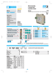
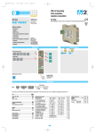
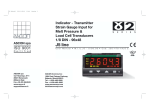
D8-ed2-IT-UK-uso
10-11-2009
17:52
Pagina 6
DIN rail mounting,
6 inputs, 2 timers and 2 outputs
digital I/O module
E
S
E
R
I
ASCON spa
D8 line
User manual
ISO 9 0 0 1
certified
User Manual • M.U. D8-2/08.08 • Cod. J30-478-1AD8 IE
ASCON spa
Via Falzarego 9/11
20021 Baranzate
(MI) Italy
Fax +39 02 350 4243
http://www.ascon.it
e-mail [email protected]
Resources
Inputs
Outputs
DI1
DO1
DI2
DO2
DI3
DI4
DI5
DI6
D8
Available functions
Not
Toggle
Available functions
Modbus RS485
Parameterisation
Supervision
Flip-Flop
Not
Hold
Duty cycle Timer
(option)
Model code
Configuration
Mod.
D 8
5 B 5 0 - 0 F 0 0 / I L 0 0 - 0 0 0 0
Line
Basic
Accessories
1st part
2nd part
The product code indicates the specific hardware configuration of the instrument,
that can be modified by specialized engineers only.
Line
D 8
DO1-DO2 outputs
Relay - Relay
Relay - SSR Drive
SSR drive - SSR drive
SSR - SSR
SSR - SSR drive
B
1
2
3
4
5
User manual
Italian/English (standard)
French/English
German/English
Spanish/English
F
0
1
2
3
Output type
No PWM output
PWM output on DO2
PWM output on DO1 and DO2
Special Functions
None
2 Timers
E
0
2
Input type
No frequency input
Frequency input on DI1
Frequency input on DI1 and DI2
I
0
1
2
Notes:
[1] Only when B = 2, 3, 4 and 5;
[2] Only when B = 3, 4 and 5.
1
S
c
D8 line
Table of contents
- Resources and output configuration;
- Model code;
- Description and table of parameters;
- Technical specifications;
- Timers.
E
[1]
[2]
L
0
1
2
D8-ed2-IT-UK-uso
10-11-2009
17:52
Pagina 7
DO_ output Duty Cycle of PWM - Table 7
DC.O_
Configuration parameters description
Parameter
Configuration parameters, shown in the table at page 3 have been divided into groups
with homogeneous functionalities. The parameters described hereafter are in the same
order as they are listed in the parameters table.
DC.O_
Configuration
PWM.f
Value
Function
0...10000 1 = 0,1 Hz, 10000 = 1kHz
DO_ output Duty Cycle 0... 1000
T
t.F.I_
Nt.I_
Description
Input filter
time
Input
status
Description
NOT (negate) DI_
Value
0
1
Function
Disables negate input status (DI_ = DI1... DI6)
Negates input status (DI_ = DI1... DI6)
On
Off
Description
NOT (negate) DO_
Internal
logic
status
Enable
NOT
function
Output
status
Value
0
1
FF.I_
Input
S
On
Off
0
0
1
1
On
Off
HL.O_
On
Off
Parameter
HL.O_
Internal
logic
status
Enable
HOLD
signal
Output
status
Parameters, shown in the table at page 3 have been divided into groups with
homogeneous functionalities. The parameters described hereafter are in the same
order as they are listed in the parameters table.
Parameters
DO.O_
Output status at power ON - Table 5
Description
DO_ at power ON
Value
0
1
Function
Output OFF at power ON (DO_ = DO1, DO2)
Output ON at power ON (DO_ = DO1, DO2)
Addr
Value
Duty Cycle at power ON - Table 6
Parameter
Description
DT.O_
DC_ at power ON
Value
0...1000
R
0
1
0
1
Function
Manages an internal logic status connected
to the inputs as a bistable type SR register
(DI_ = DI1...DI6)
Bistable (type SR); it changes the value of the
register Q to 1 at the leading edge of the SET
input signal and changes the value register Q to
0 at the leading edge of the RESET input signal.
SET and RESET inputs are couples of phisycal
inputs that cannot be changed (DI1 and DI2,
DI3 and DI4, DI5 and DI6).
DI1, DI3 and DI5 are SET inputs,
DI2, DI4 and DI6 are RESET inputs.
Internal logic
status (SR)
Unchanged
0
1
0
DO_ HOLD- Table 10
Description
HOLD output DO_
Value
0
1
On
Off
On
Off
Function
Releases the output status (DO_ = DO1, DO2)
“Freezes” the output status (DO_ = DO1, DO2)
The HOLD output command freezes the status of a phisycal output (DO1 or DO2) to the
actual value. As long as the HOLD command
is active, if the internal logic status changes,
the corresponding output status does not
change.
On
Off
Communications address
This parameter can be set between 1...247 and must be unique (no other instrument
connected to a supervisor can have the same number).
It allows to specify, separately for each output (DO1, DO2), which status the physical
output must assume at power ON independently from the last written value.
DT.O_
Description
DI_ input Flip-Flop
Function
Disables negate output status (DO_ = DO1, DO2)
Negates output status (DO_ = DO1, DO2)
Parameters description
Parameter
DI_ Flip-Flop - Table 9
FF.I_
It is possible to enable, separately for each
output (DO1and DO2), the negate (NOT) fuction of the output internal logic status.
Function
Manages an internal logic status connected
to the inputs as a bistable type T register
(DI_ = DI1...DI6)
Bistable that changes its status at the leading
edge of the input signal. An internal logic status
(T) is connected to each input. The internal logic
status value changes every time the input status changes from 0 to 1.
On
Off
Negate (NOT) output status - Table 4
Parameter
DO.O_
Value
DI_ input Toggle
Parameter
Note:The NOT command influences also the
status of the Toggle (TG.I_) and FlipFlop (FF.I_) functions (see “Logic function diagram” at page 3).
On
Off
Description
Internal
On
logic
status (T) Off
Is possible to enable, separately for each
input (DI1...DI6), the negate (NOT) fuction of
the physical input status in order to operate
in inverted logic.
On
Off
DI_ Toggle - Table 8
TG.I_
Parameter
Negate (NOT) input status - Table 3
Enable
NOT
function
Internal
logic
status
Nt.O_
0...255
Function
Allows the user to set, separately for each
input (DI_ = DI1... DI6), a filtering time with
steps of 16 ms (0 = disabled,
1 = 16ms, 255 = 4080ms)
TG.I_
Input
status
Nt.O_
Value
In order to eliminate problems caused by disturbances, the user can define the
minimum signal width (input time). The input filter is made by units of 16ms
(1... 255 units). Value 0 disables the input filter.
Parameter
Nt.I_
T
filter time for DI_ inputs - Table 2
Parameter
Function
It set the time an output stays ON as a
percentage of the total PWM period
(DO_ = DO1 and DO2)
When the SSR or SSR drive outputs have
been selected as PWM output with a specific
frequency, the Duty Cycle value of each output (ON output period expressed as a percentage of the PWM period) can be specified.
The Duty Cycle of each output can be selected through the parameter DC.O_ which
allows the following values:
0... 1000 (0 = 0%; 1000 = 100%).
T = PWM period
[s]
1
PWM frequency =
[Hz]
T
Duty cycle = T1 x 100 [%]
T
T1
PWM
output On
Off
Both outputs, when selected as SSR or SSR drive can be configured as PWM
(Pulse Width Modulation) outputs with adjustable frequency and Duty Cycle. PWM
frequency is applied to both DO1 and DO2 outputs (see also DC.O_ parameter).
t.F.I_
Value
Internal
logic On
status Off
PWM frequency for both DO1 and DO2 - Table 1
Parameter
Description
PWM.f
PWM frequency
Description
Function
Duty Cycle at power ON
It allows to specify, separately for each output (DO1, DO2), the Duty Cycle (ON output
period expressed as a percentage of the total PWM period) the module must use
at power ON, independently from the last value written in the DC.O_ parameters.
2
D8-ed2-IT-UK-uso
10-11-2009
17:52
Pagina 8
Table of standard parameters
Serial communications connection example
Configuration parameters
Configuration
D8
Configuration
tools Cd-Rom
RS485
For SCADA
Mnemonic
Parameter description
code
PWM.f
PWM frequency
Input filter time
t.F.I_
baud
Baud rate
Nt.I_
Nt.O_
Prot
Negate (NOT) DI_
Negate (NOT) DO_
Communications protocol
Range
0...10000
1...255
1200, 2400,
4800, 9600
0/1
0/1
M.bus/Jbus
PC with
Autolink
D8 - Max. 31 instruments
RS485
Local control
RS485
1/10 of Hz
Steps of 16ms
Baud
Notes
See table 1 at page 2
See table 2 at page 2
9600
0
0
M.bus
See table 3 at page 2
See table 4 at page 2
Parameters
Mnemonic
code
DO.O_
DT.O_
DC.O_
TG.I_
FF.I_
HL.O_
Addr
Parameter description
Range
Factory
setting
0
0
0
Unit
Output status at power ON 0, 1
Duty cycle DO_ at power ON 0...1000
Duty Cycle output DO_
0...1000
Toggle
0, 1
Flip-Flop
0, 1
Hold DO_ output
0, 1
Serial communication address 1...247
OP35
operator
panel
D8 - Max. 31 istruments
Factory
setting
0
0
Unit
Steps of 0.1%
Steps of 0.1%
0
247
Notes
See table 5 at page 2
See table 6 at page 2
See table 7 at page 2
See table 8 at page 2
See table 9 at page 2
See table 10 at page 2
Technical specification
Description
Features
(at 25°C env. temperature)
Using the configuration tools on a PC it is possible to choose:
- Input type - Functions to elaborate inputs/outputs - Output type
Total configurability
6 digital inputs in 2 groups (DI1, DI2 and DI3, DI4, DI5, DI6), optoisolated
Communications parameters reset
µP
Relay
Frequency inputs (DI1 and DI2) 0.1...10 kHz
No voltage inputs
Minimum pulse width: 16 ms (table 2)
Outputs
SPST relay contact:
SSR:
SSR drive:
2A/250Vac (4A/120Vac) for resistive loads;
1A/250Vac for resistive loads;
5Vdc ±20%, max. 30mA
Serial communications
Isolated RS485, protocol Modbus/Jbus, 1200, 2400, 4800, 9600 bit/s, 2 wires
Operational safety
Parameters
6
Parameters and configuration data are stored in
a non volatile memory for an unlimited time
24Vac (-25...+12%) 50/60Hz and Power consumption
24Vdc (-15...+25%)
3.2W max.
Power supply
(PTC protected)
General characteristics
Safety
EN61010-1 (IEC1010-1) installation class 2 (2.5kV),
pollution degree 2, instrument class II
Electromagnetic compatibility
Compliance to CE standards
Protection
Terminal block: IP20
UL and cUL approval
File E176452
Dimensions
Pitch: 22.5 mm - depth: 114.5 mm
Logic-function diagrams
Inputs
NOT
enable
Internal
logic status
Not
T
2
Relay
Inputs
2
5
5
JP2
1
6
JP1
1
The serial communications parameters can be reset to the original factory settings (protocol: Modbus, Baud Rate: 9600,
Address: 247).
The instructions to remove/re-insert the I/O module from/in its
plastic case are described in the “Installation manual”.
After having removed the I/O module, use the instructions that
follow to reset the communications parameters:
1) Use a jumper to short-circuit the terminals shown in the drawing that follows;
2) Insert the I/O module in its housing and power ON the instrument;
3) Power OFF the instrument, extract the I/O module from its plastic case and remove the short circuit jumper;
4) Reinstall the module in its housing.
At the end to this procedure, the communications parameters will
be reset to its factory settings.
Compatible with EN61131-2 standard:
- logic status voltage 1 ≥ 5Vdc;
- logic status voltage 0 ≤ 2Vdc;
- max. voltage allowed: 24Vdc
Voltage inputs
Input from
the field
Filter
TOGGLE
LED
SET input
In order to reset the serial communication
parameters to their default values, use a
junper to short-circuit the indicated
terminals
FLIP-FLOP
From RESET
input
Outputs
Warranty
HOLD
enable
NOT
enable
HOLD
We warrant that the products will be free from defects
in material and workmanship for 3 years from the date
of delivery.
The warranty above shall not apply for any failure
caused by the use of the product not in line with the
instructions reported on this manual.
PWM
enable
Not
Internal
logic status
PWM
Output status
at power ON
Frequency
LED
Duty Cycle
at power ON
3
Output
to the
field
Duty Cycle
D8-ed2-IT-UK-uso
10-11-2009
17:52
Pagina 5
Timer
Description
Up to 2 timers can be activated in the instrument. The term “timer” for this instrument means all the functionalities connected to Digital Inputs, Digitl outputs and internal variables conditioned by a free-running counter that has a settable time base.
Timer types
Four types of timer can be set:
• Free Run;
• Pulse;
• Countdown;
• Countdown Latched.
The following parameters must be doubled: one set for Timer1 and 1 set for Timer2.
Configuration
Mnemonic
code
TbTp
TbOn
Tp
TOn
Parameter description
Time base for the Period (Tp)
Time base for TOn
Period value
ON time value
TTm
Timer Type
Range
Unit
0, 1, 2
S, Min, Hour
0, 1, 2
S, Min, Hour
1… 32000
1… 32000
None; FreeRun; Pulse; Countdown;
Countdown Latched
Factory
setting
0
0
0
0
The values must be referred to the
respective time base
None
Trig
Digital Input associated to the Trigger
None; DI1, DI2
None
Rst
Digital Input associated to the Reset
None; DI1, DI2
None
Out
Digital Output associated to the Timer
None; DO1, DO2
None
Timer enable value at Power ON
0,1
TEnP
Notes
he Timer is active when the selected Digital Input
is enabled (TEn = ON).
If no Digital Input is selected (None), the timer is
active depending on the Trigger status in the
instrument memory (TrRa).
More than one funtion can be assigned to the
same physical output. The Output status is the
OR of the sources
0
Parameters
Mnemonic
code
Parameter description
Range
Unit
Factory
setting
TEn
Timer enable
0, 1
0
TrRa
Trigger in memory
0, 1
0
TRes
TEv
Memory Reset
Events
0, 1
Read only: 0, 1
0
Notes
At Start-Up this parameter is initialized to
the TEnP value
For “Free Run” only, at Start-Up this
parameter is initialized to the TEnP value
Operating modes
Free Run Timer
The user must define the Time period (Tp) and the duration
of the periodic event (TOn). With Timer enabled (TEn = ON)
and Trigger = ON the instrument generates the Event
having a duration = TOn and periodicity = Tp, in continuous
mode. Reset = ON pauses the Event generation.
CountDown Timer
With Timer enabled (TEn = ON) the instrument generates
the Event after a delay having a duration = Tp starting at
Trigger = ON. The Event is maintained until the Trigger
value goes OFF. Reset = ON pauses the Event generation.
CountDown Latched Timer
With Timer enabled (TEn = ON) the instrument generates
the Event after a delay having a duration = Tp starting at
Trigger = ON. The Event is maintained until the Reset
value goes ON (once the event is activated is independent
from TEn signal); Reset = ON pauses the Event generation.
Ton
Tp
Tp
Tp
Trigger
Trigger
Trigger
Reset
Pulse timer
With Timer enabled (TEn = ON) and Trigger = ON the
instrument generates the Event having a duration = Tp
starting at Trigger = OFF. Reset = ON pauses the Event
generation.
To activate the Evento, Trigger must be active (ON) for a
time longer than TP.
Tp
Trigger
4