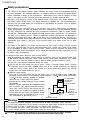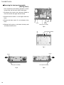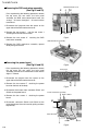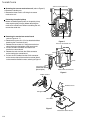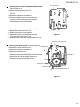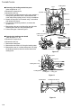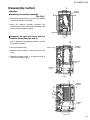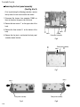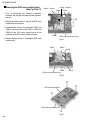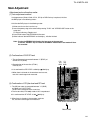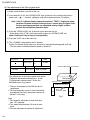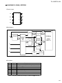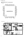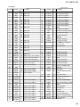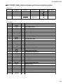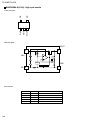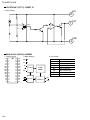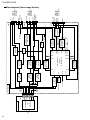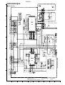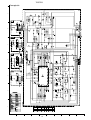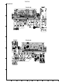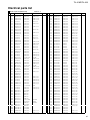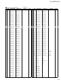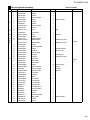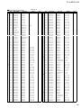
1
TH-A10R/TH-A10
TH-A10R/TH-A10
SERVICE MANUAL
DVD DIGITAL THEATER SYSTEM
TH-A10R
TH-A10
SP-PWA10
RM-STHA10R
SP-XSA10
SP-XSA10
SP-XCA10
RM-STHA10EC
XV-THA10R
Area Suffix
TH-A10R
B
EN
EE
TH-A10R
TH-A10
U.K.
Northern Europe
Russia
Area Suffix
TH-A10
E
Continental Europe
XV-THA10R (DVD player)/XV-TH-A10
SP-PWA10 (Powered subwoofer)
SP-THA10
SP-XCA10 (Center speaker)
(Speaker section)
SP-XSA10 (Satellite speaker) x 4
Contents
Safety Precautions
Important for laser products
Preventing static electricity
Disassembly method
Adjustment method
VICTOR COMPANY OF JAPAN, LIMITED
OPTICAL DISC BUSINESS DIV. PERSONAL & MOBILE NETWORK BUSINESS UNIT
AV & MULTIMEDIA COMPANY 1644, Shimotsuruma, Yamato, Kanagawa 242-8514, Japan
No.20872
Printed in Japan
200009(S)
COPYRIGHT
1-2
1-3
1-4
1-5
1-21
Flow of functional operation
until TOC read
Maintenance of laser pickup
Replacement of laser pickup
Description of major ICs
2000 VICTOR COMPANY OF JAPAN, LTD.
1-24
1-25
1-25
1-26
No.20872
Sep. 2000
TH-A10R/TH-A10
Safety precautions
1. This design of this product contains special hardware and many circuits and components specially
for safety purposes. For continued protection, no changes should be made to the original design
unless authorized in writing by the manufacturer. Replacement parts must be identical to those
used in the original circuits. Services should be performed by qualified personnel only.
2. Alterations of the design or circuitry of the product should not be made. Any design alterations of
the product should not be made. Any design alterations or additions will void the manufacturer`s
warranty and will further relieve the manufacture of responsibility for personal injury or property
damage resulting therefrom.
3. Many electrical and mechanical parts in the products have special safety-related characteristics.
These characteristics are often not evident from visual inspection nor can the protection afforded
by them necessarily be obtained by using replacement components rated for higher voltage,
wattage, etc. Replacement parts which have these special safety characteristics are identified in
the Parts List of Service Manual. Electrical components having such features are identified by
shading on the schematics and by ( ) on the Parts List in the Service Manual. The use of a
substitute replacement which does not have the same safety characteristics as the recommended
replacement parts shown in the Parts List of Service Manual may create shock, fire, or other
hazards.
4. The leads in the products are routed and dressed with ties, clamps, tubings, barriers and the
like to be separated from live parts, high temperature parts, moving parts and/or sharp edges
for the prevention of electric shock and fire hazard. When service is required, the original lead
routing and dress should be observed, and it should be confirmed that they have been returned
to normal, after re-assembling.
5. Leakage currnet check (Electrical shock hazard testing)
After re-assembling the product, always perform an isolation check on the exposed metal parts
of the product (antenna terminals, knobs, metal cabinet, screw heads, headphone jack, control
shafts, etc.) to be sure the product is safe to operate without danger of electrical shock.
Do not use a line isolation transformer during this check.
Plug the AC line cord directly into the AC outlet. Using a "Leakage Current Tester", measure
the leakage current from each exposed metal parts of the cabinet , particularly any exposed
metal part having a return path to the chassis, to a known good earth ground. Any leakage
current must not exceed 0.5mA AC (r.m.s.)
Alternate check method
Plug the AC line cord directly into the AC outlet. Use an AC voltmeter having, 1,000 ohms
per volt or more sensitivity in the following manner. Connect a 1,500 10W resistor paralleled by
a 0.15 F AC-type capacitor between an exposed
AC VOLTMETER
metal part and a known good earth ground.
(Having 1000
Measure the AC voltage across the resistor with the
ohms/volts,
or more sensitivity)
AC voltmeter.
Move the resistor connection to eachexposed metal
part, particularly any exposed metal part having a
0.15 F AC TYPE
return path to the chassis, and meausre the AC
Place this
voltage across the resistor. Now, reverse the plug in
probe on
the AC outlet and repeat each measurement. voltage
each exposed
1500 10W
metal part.
measured Any must not exceed 0.75 V AC (r.m.s.).
This corresponds to 0.5 mA AC (r.m.s.).
Good earth ground
Warning
1. This equipment has been designed and manufactured to meet international safety standards.
2. It is the legal responsibility of the repairer to ensure that these safety standards are maintained.
3. Repairs must be made in accordance with the relevant safety standards.
4. It is essential that safety critical components are replaced by approved parts.
5. If mains voltage selector is provided, check setting for local voltage.
! CAUTION Burrs formed during molding may be left over on some parts of the chassis. Therefore,
pay attention to such burrs in the case of preforming repair of this system.
1-2
TH-A10R/TH-A10
Preventing static electricity
Electrostatic discharge (ESD), which occurs when static electricity stored in the body, fabric, etc. is discharged,
can destroy the laser diode in the traverse unit (optical pickup). Take care to prevent this when performing repairs.
1.1. Grounding to prevent damage by static electricity
Static electricity in the work area can destroy the optical pickup (laser diode) in devices such as DVD players.
Be careful to use proper grounding in the area where repairs are being performed.
1.1.1. Ground the workbench
1. Ground the workbench by laying conductive material (such as a conductive sheet) or an iron plate over
it before placing the traverse unit (optical pickup) on it.
1.1.2. Ground yourself
1. Use an anti-static wrist strap to release any static electricity built up in your body.
(caption)
Anti-static wrist strap
Conductive material
(conductive sheet) or iron plate
1.1.3. Handling the optical pickup
1. In order to maintain quality during transport and before installation, both sides of the laser diode on the
replacement optical pickup are shorted. After replacement, return the shorted parts to their original condition.
(Refer to the text.)
2. Do not use a tester to check the condition of the laser diode in the optical pickup. The tester's internal power
source can easily destroy the laser diode.
1.2. Handling the traverse unit (optical pickup)
1. Do not subject the traverse unit (optical pickup) to strong shocks, as it is a sensitive, complex unit.
2. Cut off the shorted part of the flexible cable using nippers, etc. after replacing the optical pickup. For specific
details, refer to the replacement procedure in the text. Remove the anti-static pin when replacing the traverse
unit. Be careful not to take too long a time when attaching it to the connector.
3. Handle the flexible cable carefully as it may break when subjected to strong force.
4. It is not possible to adjust the semi-fixed resistor that adjusts the laser power. Do not turn it
1-3
TH-A10R/TH-A10
Dismantling and assembling the traverse unit
1. Notice regarding replacement of optical pickup
Electrostatic discharge (ESD), which occurs when static electricity stored in the body, fabric, etc. is discharged,
can destroy the laser diode in the traverse unit (optical pickup). Take care to prevent this when performing
repairs to the optical pickup or connected devices.
(Refer to the section regarding anti-static measures.)
1. Do not touch the area around the laser diode and actuator.
2. Do not check the laser diode using a tester, as the diode may easily be destroyed.
3. It is recommended that you use a grounded soldering iron when shorting or removing the laser diode.
Recommended soldering iron: HAKKO ESD-compatible product
4. Solder the land on the optical pickup's flexible cable.
Note : Short the land after shorting the terminal on the flexible cable using a clip, etc., when using an
ungrounded soldering iron.
Note : After shorting the laser diode according to the procedure above, remove the solder according
to the text explanation.
Laser pick-up unit
Flexible cable
Short circuit land
Shorting
Shot with the rclip
1-4
TH-A10R/TH-A10
Disassembly method
A
Top cover
<Main body>
A
Removing the top cover
(See Fig.1 and 2)
1. Remove the four screws A attaching the top cover
(Use an Allen wrench).
2. Lift up the front part of the top cover to release the
two joints a and remove the top cover toward the
front.
Joints a
Fig.1
Removing the rear cover (See Fig. 3)
Top cover
Prior to performing the following procedure, remove
the top cover.
1. Remove the four screws B attaching the rear cover
on the back of the body. Pull out the rear cover
backward.
Joint a
Removing the right and left side covers
(See Fig. 4 and 5)
Fig.2
Prior to performing the following procedure, remove
the top cover and the rear cover.
B
Rear cover
B
1. Move the left side cover backward to release the five
joint hooks b and remove the left side cover outward.
2. Remove the right side cover in the same way.
B
B
Fig.3
Right side cover
Left side cover
Joints b
Joints b
Fig.5
Fig.4
1-5
TH-A10R/TH-A10
Removing the front panel assembly
(See Fig. 6 to 9)
Prior to performing the following procedure, remove
the top cover, the rear cover and the side covers.
1. Disconnect the harness from connector CN802 on
the main board on the upper side of the body.
2. Remove the two screws C on the upper side of the
body.
3. Remove the three screws D on the bottom of the
body.
C Joint c
4. Release the five joints c and detach the front panel
assembly toward the front.
Joint c
CN802
Front panel assembly
C
Fig.6
D
Front panel assembly
Joint c
D
Fig.7
Joint c
Joint c
Front panel assembly
Fig.9
1-6
Front panel assembly
Fig.8
TH-A10R/TH-A10
Removing the right and left corner
covers (See Fig.10 and 11)
Prior to performing the following procedure, remove
the top cover, the rear cover, the side covers and the
front panel assembly.
It is not necessary to remove the front panel
assembly.
Joint d
1. Move the left corner cover backward to release the
three joint hooks d.
Left corner cover
Joints d
Fig.10
2. Remove the right corner cover in the same way.
Removing the rear panel
(See Fig.12 to 14)
Prior to performing the following procedure, remove
the top cover and the rear cover.
Joint d
Joints d
Right corner cover
1. Remove the eighteen screws E and the one screw F
attaching the rear panel.
Fig.11
2. Release the two joints e on both sides of the body.
E
E
E
F
Rear panel
E
E
E
E
Fig.12
Joint e
Joint e
Rear panel
Rear panel
Fig.12
Fig.12
1-7
TH-A10R/TH-A10
Removing the DVD servo control board
(See Fig.15 to 17)
Digital I / O board
Analog I / O board
CN681
CN201
Prior to performing the following procedure,
remcover and the right side cover.ove the top cover,
the rear
G
1. Remove the three screws G and pull the DVD servo
control board case upward.
2. Disconnect the harness from connector CN501 and
CN503, and the card wire from CN101, CN103 and
CN502 of the DVD servo control board on the
underside of the DVD servo control board case.
CN687
3. Remove the four screws H attaching the DVD servo
control board.
DVD servo control board (case)
Fig.15
CN503
CN501
CN502
CN101
CN103
DVD servo control board case
Fig.16
H
H
DVD servo control board
H
DVD servo control board case
H
Fig.17
1-8
TH-A10R/TH-A10
Removing the analog I / O board / the
digital I / O board (See Fig.18 and 19)
Digital I / O board
Analog I / O board
CN681
CN201
Prior to performing the following procedure, remove
the top cover and the rear cover.
G
1. Remove the two screws E attaching the analog I / O
board on the back of the body.
2. Disconnect the card wire from connector CN201 on
the analog I / O board.
3. Remove the four screws E attaching the digital I / O
board on the back of the body.
CN687
DVD servo control board (case)
4. Disconnect the card wire from connector CN681 and
CN687 on the digital I / O board.
Fig.18
Removing the tuner board / the sub
board (See Fig.20 and 21)
E
E
E
Rear panel
Prior to performing the following procedure, remove
the top cover, the rear cover and the DVD servo
control board case.
1. Remove the two screws E attaching the tuner board
on the back of the body.
Fig.19
2. Disconnect connector CN111 on the tuner board
from the sub board.
3. Disconnect connector CN131 on the sub board from
the main board.
CN111
Sub board
Tuner board
Sub board
CN131
E
Fig.21
Fig.20
1-9
TH-A10R/TH-A10
DVD mechanism cover
Removing the DVD mechanism assembly
(See Fig.22 and 23)
J
K
K
Prior to performing the following procedure, remove
the top cover, the rear cover, the front panel
assembly, the DVD servo control board case, the
analog I / O board, the digital I / O board and the
tuner board.
1. Disconnect the harnesses from the spacer on the
upper side of the DVD mechanism cover.
2. Remove the two screws I and the one screw J
attaching the DVD mechanism cover.
3. Remove the two screws K
mechanism assembly.
I
Spacer
I
Fig.22
attaching the DVD
DVD mechanism assembly
4. Remove the DVD mechanism assembly upward
while pulling it backward.
Removing the power board
(See Fig.24 and 25)
Fig.23
Prior to performing the following procedure, remove
the top cover, the rear cover, the front panel
assembly, the DVD servo control board case and the
digital I / O board.
Rear panel
1. Disconnect the harness from the spacer on the
upper side of the DVD mechanism cover.
2. Remove the two screws E attaching the power
board on the back of the body.
3. Disconnect the harness from connector CN911 and
CN912 on the power board.
Fig.24
E
E
Power transformer assembly
CN911,CN912
4. Remove the four screws L
board.
attaching the power
5. Disconnect connector CN913 and CN914 of the
power board from the main board by pulling out them
respectively.
L
M
L
Power board
L
CN914
Fig.25
1-10
CN913
Spacer
TH-A10R/TH-A10
Rear panel
Removing the power transformer assembly
(See Fig.24 and 25)
Prior to performing the following procedures, remove
the top cover and the rear cover.
1. Disconnect the harnesses from connector CN911
and CN912 on the power board.
2. Remove the two screws M
transformer assembly.
E
E
Fig.24
attaching the power
CN911,CN912
3. Remove the screw E
attaching the power
transformer assembly on the back of the body.
L
M
Removing the main board (See Fig.26)
Prior to performing the following procedure, remove
the top cover, the rear cover, the front panel
assembly, the rear panel, the DVD mechanism
assembly, the power board and the sub board.
L
Power board
1. Remove the four DVD spacers on the upper side of
the main board.
CN914
L
2. Remove the five screws N attaching the main board.
CN913
Spacer
Fig.25
N
Mainboard
N
<Front panel assembly>
Prior to performing the following procedure, remove
the top cover, the rear cover, the side covers and the
front panel assembly.
Removing the power switch board
(See Fig.27)
1. Dithe harness from connector CN705 on the power
switch board.sconnect
2. Remove the three screws O
switch board.
Fig.26
N
attaching the power
CN706
IC board
R
Power switch board
O
O
LED board
S
Fig.27
1-11
TH-A10R/TH-A10
Removing the eject board (See Fig.28)
Eject board
Switch board
1. Disconnect the harness from connector CN702 on
the eject board.
2. Remove the three screws P
board.
attaching the eject
Removing the LCD board (See Fig.29)
P
CN702
T
1. Remove the four screws Q attaching the LCD board.
Fig.28
2. Unsolder WA701, WA703 and WA704 on the LCD
board.
Q
Q
Removing the IC board (See Fig.27)
1. Remove the screw R attaching the IC board.
2. Disconnect the harness from connector CN706 on
the IC board.
WA704
WA703
LCD board
WA701
Q
Removing the LED board (See Fig.27)
Q
Fig.29
Prior to performing the following procedure, remove
the LCD board and the IC board.
1. Disconnect the harness from connector CN705 on
the power switch board.
CN706
IC board
R
Power switch board
2. Remove the two screws S attaching the LED board.
O
O
Removing the switch board (See Fig.28)
Prior to performing the following procedure, remove
the LCD board.
1. Disconnect the harness from connector CN702 on
the eject board.
2. Remove the two screws T
board.
1-12
attaching the switch
LED board
S
Fig.27
TH-A10R/TH-A10
Loading tray
<Removing DVD mechanism unit>
Removing the clamper base (refer to Figure 1)
o Remove the top cover.
o Remove the DVD mechanism unit.
1. Remove the two screws at A fixing the clamper base.
Clamper base
Removing the loading tray (refer to Figures 2 - 4)
o Remove the clamper base.
1. Turn the up-down cam lever clockwise (in the direction
of the arrow in Figure 2) to lower the position of the mechanism.
2. Manually set the loading tray to the fully-open position.
3. Stretch the tray stoppers on both sides of the loading
base outward and pull out the tray.
Figure 1
Loading tray (front side)
Loading base
Up-down cam
Tray stopper
Lever
Loading base
Figure 2
Loading tray
Loading tray
Push
Push
Tray stopper
Figure 4
Figure 3
1-13
TH-A10R/TH-A10
Traverse mechanism unit
Removing the traverse mechanism unit (refer to Figure 5)
o Remove the loading tray.
1. Remove the three screws at B fixing the traverse
mechanism unit.
B
Protecting the optical pickup
o Solder the flexible ground point on the optical pickup
when replacing the pickup or before detaching the
mechanism control board. When assembling the unit,
remove the solder last.
Removing the mechanism control board
(refer to Figures 6 - 7)
o Remove the traverse unit. (Can be detached without
detaching the T-mechanism unit.)
1. Remove the two screws at C fixing the mechanism
control base from the bottom of the traverse unit.
2. Pull out the CN12 connector and detach the
mechanism control board.
3. Remove the card wire from the CN13 connector
on the mechanism control board.
4. Pull out the FPC holder from the CN12 connector
on the reverse side of the mechanism control board
and remove the flexible harness, referring to Figure 7.
B
B
Figure 5
Traverse mechanism unit
C
CN12
Enlargement
CN13
Connection area
(Solder the flexible
ground point)
Mechanism control board
Figure 6
Flexible harness
Flexible harness
3
Enlargement
2
FPC holder
1
CN12
Figure 7
Mechanism control board
1-14
TH-A10R/TH-A10
Traverse chassis
Removeing the turntable and spindle motor assemby
(refer to Figures 8 - 9)
o Remove the traverse mechanism unit.
o Solder the flexible ground point on the optical pickup.
(Figure 6)
o Remove the mechanism control board.
1. Remove the flexible harness from the feed motor
connector on the spindle motor board assembly.
2. Remove the three screws at D fixing the spindle motor
from the bottom of the traverse chassis.
Removing the feed motor unit (refer to Figure 9)
o Remove the traverse mechanism unit.
o Remove the mechanism control board.
1. Remove the FPC from the feed motor connector
on the turntable spindle motor board.
2. Remove the two screws at E fixing the feed motor unit.
D
Figure 8
Traverse mechanism unit
F
Pick-up assembly
Removing the optical pickup unit (refer to Figure 9)
Guide shaft B
o Remove the traverse mechanism unit.
o Remove the mechanism control board.
E
o Remove the feed motor unit.
1. Remove the screw at F fixing the guide shaft holder at B,
then simultaneously remove the guide shaft at B and the
optical pickup unit. While doing so, slide the unit
horizontally away from the guide shaft at A.
E
Guide shaft A
Feed motor assembly
Flexible harness
Turn table spindle motor unit
Feed motor connector
Figure 9
1-15
TH-A10R/TH-A10
Loading base
Lever
Removeing the loading mechanism parts
(refer to Figures 10 - 11)
o Remove the clamper base.
Up-down cam
o Remove the disk tray.
1. Turn the lever counterclockwise until it stops (position 1),
while pushing the switch lever in the direction of the
arrow and pushing up the pawl at A using a screwdriver.
2. Stretch the two pawls at B outward using a screwdriver
and remove the chassis.
3. Turn the lever clockwise (position 2) to remove the
up-down cam.
Pawl B
4. Remove the pulley gear and the pulley gear belt after
removing the screw at G fixing the pulley gear.
5. Pull out drive gear 2 then drive gear 1.
G
2
1
Pawl A
Chassis
Pawl B
Switch lever
(1)When detaching
the chassis.
Removing the loading motor board
(refer to Figures 11 - 12)
o Remove the clamper base.
o Remove the disk tray.
1. Remove the loading belt.
2. Remove the two screws at H fixing the loading motor.
3. Remove the screw at I and the three pawls at C fixing
the loading motor base from the reverse side of the
loading base.
(2)When detaching
the up-down cam.
chassis.
Up-down cam
G
Up-down cam
Switch lever
G
Figure 10
Drive gear 1
Drive gear 2
H
Loading motor unit
H
G
Loading base
Loading belt
Pulley gear
Figure 11
Loading base
Loading motor board
I
Pawl C
Figure 12
1-16
TH-A10R/TH-A10
Disassembly method
A
<Speaker>
Removing the amplifier assembly
(See Fig.1)
Amplifier
assembly
A
A
1. Remove the twelve screws A attaching the amplifier
assembly on the back of the body.
2. Move the amplifier assembly backward and
disconnect the harness from connector CN109 in the
lower part of the amplifier assembly.
CN109
A
Removing the heat sink cover and the
amplifier cover (See Fig.2 and 3)
Fig.1
Prior to performing the following procedure, remove
the amplifier assembly.
1. Pull out the volume knob.
B
Amplifier
assembly
Volume knob
2. Remove the four screws B attaching the heat sink
cover.
3. Remove the twenty screws C and the one screw D
attaching the amplifier cover.
Heat sink
cover
Amplifier
cover
Fig.2
B
C
Amplifier
assembly
C
C
D
C
C
Amplifier
cover
C
Fig.3
C
1-17
TH-A10R/TH-A10
Removing the front panel assembly
(See Fig. 6 to 9)
Prior to performing the following procedure, remove
the top cover, the rear cover and the side covers.
1. Disconnect the harness from connector CN802 on
the main board on the upper side of the body.
2. Remove the two screws C on the upper side of the
body.
3. Remove the three screws D on the bottom of the
body.
C Joint c
4. Release the five joints c and detach the front panel
assembly toward the front.
Joint c
CN802
Front panel assembly
C
Fig.6
D
Front panel assembly
Joint c
D
Fig.7
Joint c
Joint c
Front panel assembly
Fig.9
1-18
Front panel assembly
Fig.8
TH-A10R/TH-A10
Removing the right and left corner
covers (See Fig.10 and 11)
Prior to performing the following procedure, remove
the top cover, the rear cover, the side covers and the
front panel assembly.
It is not necessary to remove the front panel
assembly.
Joint d
1. Move the left corner cover backward to release the
three joint hooks d.
Left corner cover
Joints d
Fig.10
2. Remove the right corner cover in the same way.
Removing the rear panel
(See Fig.12 to 14)
Prior to performing the following procedure, remove
the top cover and the rear cover.
Joint d
Joints d
Right corner cover
1. Remove the eighteen screws E and the one screw F
attaching the rear panel.
Fig.11
2. Release the two joints e on both sides of the body.
E
E
E
F
Rear panel
E
E
E
E
Fig.12
Joint e
Joint e
Rear panel
Rear panel
Fig.12
Fig.12
1-19
TH-A10R/TH-A10
Removing the DVD servo control board
(See Fig.15 to 17)
Digital I / O board
Analog I / O board
CN681
CN201
Prior to performing the following procedure,
remcover and the right side cover.ove the top cover,
the rear
G
1. Remove the three screws G and pull the DVD servo
control board case upward.
2. Disconnect the harness from connector CN501 and
CN503, and the card wire from CN101, CN103 and
CN502 of the DVD servo control board on the
underside of the DVD servo control board case.
CN687
3. Remove the four screws H attaching the DVD servo
control board.
DVD servo control board (case)
Fig.15
CN503
CN501
CN502
CN101
CN103
DVD servo control board case
Fig.16
H
H
DVD servo control board
H
DVD servo control board case
H
Fig.17
1-20
TH-A10R/TH-A10
Main Adjustment
Adjustment and confirmation matter
(1) Auto adjustment method
If microprocessor (IC401, IC402, IC714, IC716) or DVD Prek-up is replaced, initialize
the DVD player in the following matter:
1. Initialize the DVD player in the following matter:
1) Make sure that no disc is on the tray.
2) Insert the power pulag to the outret while pressing "PLAY" and "OPEN/CLOSE" button at the
same time.
FL Display indicate ; Region cord.
3) Press Enter button. And EEPROM initialize start.
4) When indicate "96kHz EEPROM" on the display , initialize finished.
Note : During the EEPROM initialization the keys may not be operated.
Press the "POWER" key to initiate the STAND-BY mode and the test mode will then
be cancelled.
(2) Confirmation of DVD RF level
1.The oscilloscope is connected between "1"(RFOP) of
CN104 and "2"(GND).
2.Reproduction of the test disc (VT-501)
made by JVC.
P12
P1
and and
GND GND
3.It is confirmed that RF LEVEL is 350mVp-p 150mVp-p.
4.When there is disorder in the waveform road cuts etc,
test disk is exchanged and measured.
(3) Confirmation of CD jitter level and RF level
1. The CD jitter meter is connected between "11"(GND)
of CN104 and "12"(FLTOUT).
The RF level is observed at the same time.
2.The first test disk(CTS-1000) made of JVC is reproduced.
3.It is confirmed that RF LEVEL is 360 100mVp-p.
5. When there is disorder in the waveform road cuts
etc, test disk is exchanged and measured.
DVD SERVO CONTROL PWB
FRONT SIDE
1-21
TH-A10R/TH-A10
(4) Flap adjustment of the Pick-up guide shaft
1) Make sure that there is no disc on the tray.
2) Press both the "PLAY" and "OPEN/CLOSE" keys of the main unit to activate the primary
power and ∗ ∗ ( ∗ ∗ ; Version3, ; Region cord) will be displayed on the FL indicator.
Note: If the FL indicator display stops and remains at "TEST 0", unplug the power
cord from the outlet and after waiting at least 1 second, plug it in again. After
the tray open/close procedure has completed, unplug it again and then
perform the initialization procedure again.
3) Press the "OPEN/CLOSE" key of the main unit to draw the tray out.
*Place the test disk (VT-501) on the tray and then press the "OPEN/CLOSE" key.
(Note: Pushing the tray to close it is not possible.)
4) Press the "PLAY" key of the main unit.
5) The "JIT 0000" is displayed on the FL indicator.
Set the FL indicator figure value to its minimum by adjusting the pickup guide shaft flap.
* The test mode is cancelled when the power is turned off.
Measurement
Adjustment point
Refer to Fig.2
Measurement machine
No need
Mode
Reproduction
part
Disc
VT-501
connections
Extension cord No.
Refer to Fig.1
QUQ110-3740AM
CN101 of DVD Servo Control PWB
General tool : Hex-head wrench (1.27 mm)
"Flap adjustment" of the Pick-up guide shaft adjusts
"Tangential adjustment machine screw" A and
"Tilt adjustment machine screw" B from the
DVD Mechanism A'ssy bottom.
DVD player
Extension Cord
DVD Mechanism A'ssy
1. The part at the center on the DVD test disc is
reproduced.
2.The flap adjustment screws is turned alternately
and adjusted like clearly seeing the waveform of
CN104"1" to the way.
Stand
CN11 of
Connection PWB
Fig.1
Note
1.The tangential adjustment is done finish and,
then, tilt is adjusted.
2.The repeat the adjustment 2-3 times,for best
result.
3.The final adjustment should be tilt adjustment.
1-22
Stand
200mm
TH-A10R/TH-A10
Confirmation after adjustment.
A
Confirm to reproduce video CD and CD after
the DVD test disc is adjusted and to find abnormality.
B A
Fig.2
(5) About keeping the disc
As for the DVD test disc, plane accuracy is demanded.Please note the keeping place on the disc.
1. Please do not put the disc directly on the work desk etc. after uses .
2. To keep the planarity of the disc, politely handle ,and please put in a special case and keep
the disc vertically after uses .
Please keep keeping the disc in a cool place where direct sunshine and the air-conditioning
wind do not drive.
3. When the disc curves,an accurate adjustment cannot be done.
Please exchange for a new test disc and adjust optics.
4. Other discs might not be able to be reproduced when adjusting on a curved disc.
Point of adjustment
* Please execute the static electricity protection measures before starting the adjustment.
* When the following parts are exchanged,optical adjustment "Adjust the flap of the disc motor"
is necessary.
1.The disc motor was exchanged.
2.The laser pick up was exchanged.
3.The traverse motor unit was exchanged.
Note
Additionally, please adjust the flap of the disc motor when the picture quality
deterioration is seen .The basic adjustment though, is unnecessary for part exchange
in the traverse.
An optical adjustment in the laser pick up cannot be done.
Please adjust the flap of the disc motor after exchanging the laser pick up.
* When the traverse unit is exchanged, the adjustment is basically unnecessary.
1-23
TH-A10R/TH-A10
Precautions for Service
Handling of Traverse Unit and Laser Pickup
1. Do not touch any peripheral element of the pickup or the actuator.
2. The traverse unit and the pickup are precision devices and therefore must not be subjected to
strong shock.
3. Do not use a tester to examine the laser diode. (The diode can easily be destroyed by the
internal power supply of the tester.)
4. To replace the traverse unit, pull out the metal short pin for protection from charging.
5. When replacing the pickup, after mounting a new pickup, remove the solder on the short land
which is provided at the center of the flexible wire to open the circuit.
6. Half-fixed resistors for laser power adjustment are adjusted in pairs at shipment to match the
characteristics of the optical block.
Do not change the setting of these half-fixed resistors for laser power adjustment.
Destruction of Traverse Unit and Laser Pickup by Static Electricity
Laser diodes are easily destroyed by static electricity charged on clothing
or the human body. Before repairing peripheral elements of the traverse
unit or pickup, be sure to take the following electrostatic protection:
1. Wear an antistatic wrist wrap.
2. With a conductive sheet or a steel plate on the workbench on which
the traverse unit or the pick up is to be repaired, ground the sheet
or the plate.
3. After removing the flexible wire from the connector (CN101),
short-circuit the flexible wire by the metal clip.
4. Short-circuit the laser diode by soldering the land which is provided
at the center of the flexible wire for the pickup.
After completing the repair, remove the solder
to open the circuit.
Short-circuit
1-24
TH-A10R/TH-A10
Discription of major IC's
AL4527 (IC601): A/D, D/A Converters
44
43
42
41
40
39
38
37
36
35
34
CDTO
CDTI
CCLK
CS
PIS
XTO
XTI
AVSS
AVDD
VREFH
VCOM
1. Terminal layout
1
2
3
4
5
6
7
8
9
10
11
33
32
31
30
29
28
27
26
25
24
23
VREFL
RIN+
RINLIN+
LINROUT1
LOUT1
ROUT2
LOUT2
ROUT3
LOUT3
DEM1
DEM0
MCKO
DVDD
DVSS
PD
XTS
ICKS1
ICKS0
CAD1
CAD0
12
13
14
15
16
17
18
19
20
21
22
SDOS
OCKS
MIS
BCLK
LRCK
SDTI1
SDTI2
SDTI3
SDTO
DAUX
DFS
2. Block diagram
LIN+
LIN-
ADC
HPF
RIN+
RIN-
ADC
HPF
Audio
I/F
LRCK
LOUT1
LPF
DAC
DATT
BICK
DAUX
MCLK
ROUT1
LPF
DAC
DATT
LOUT2
LPF
DAC
DATT
ROUT2
LPF
DAC
DATT
SDOUT
Format
Converter
SDOS
SDTO
LOUT3
LPF
DAC
DATT
SDTI1
SDIN1
SDIN2
ROUT3
LPF
DAC
DATT
SDIN3
SDTI2
SDTI3
1-25
TH-A10R/TH-A10
3. Pin function
Pin No. Symbol
SDOS
1
OCKS
2
MIS
3
BCLK
4
LRCK
5
SDTI1
6
SDTI2
7
SDTI3
8
SDTO
9
DAUX
10
DFS
11
DEM1
12
DEM0
13
MCKO
14
DVDD
15
DVSS
16
PD
17
XTS
18
ICKS1
19
ICKS0
20
CAD1
21
CAD0
22
LOUT3
23
ROUT3
24
LOUT2
25
ROUT2
26
LOUT1
27
ROUT1
28
LIN29
LIN+
30
RIN31
RIN+
32
VREF
33
VCOM
34
VREFH
35
AVDD
36
AVSS
37
XTI
38
XTO
39
PIS
40
1-26
41
CS
42
CCLK
43
CDTI
44
CDTO
I/O
I
I
I
I
I/O
I
I
I
O
I
I
I
I
I
I
I
I
I
I
O
O
O
O
O
O
I
I
I
I
O
O
O
I
I
I
I
I
I
I
I/O
I
Functions
SDTO source select terminal L: Internal ADC output H: DAUX input
Serial control mode select terminal L: 3-wire serial H: IC bus
Soft mute terminal H: Starting Soft mute L: Cancel
Audio serial data clock terminal
Input channel clock terminal
DAC1 audio serial data input terminal
DAC2 audio serial data input terminal
DAC3 audio serial data input terminal
Audio serial data output terminal
Auxiliary audio serial data input terminal
2x sampling mode terminal L: Ordinal speed H: 2x speed
De-emphasize 1 terminal
De-emphasize 2 terminal
Power terminal for output buffer 2.7 5.5 V
Digital power supply terminal 4.5 5.5 V
Digital ground terminal 0 V
Power down & reset terminal L: Power is down and register is initialized.
Input clock selection 2 terminals
Input clock selection 1 terminals
Input clock selection 0 terminals
Chip address 1 terminal
Chip address 0 terminal
DAC3 L channel analog output terminal
DAC3 R channel analog output terminal
DAC2 L channel analog output terminal
DAC2 R channel analog output terminal
DAC1 L channel analog output terminal
DAC1 R channel analog output terminal
L channel analog reverse input terminal
L channel analog non-reverse input terminal
R channel analog reverse input terminal
R channel analog non-reverse input terminal
Zero input detection terminal L: P/S = H
COMMON voltage output terminal
Reference voltage input terminal
Analog power supply terminal 4.5 5.5 V
Analog ground terminal 0 V
Zero input detection terminal L: P/S = H
Master clock input terminal
Parallel/serial select terminal
L: Serial control mode H: Parallel control mode
Audio data interface format 0 terminal (with parallel control mode)
Chip select terminal (with 3-wire serial control mode)
Audio data interface format 0 terminal (with parallel control mode)
Control data clock terminal (with serial control mode)
Loopback mode 0 terminal (with parallel control mode)
Control data input terminal (with serial control mode)
Loopback mode 1 terminal
TH-A10R/TH-A10
AK93C65AF-X (IC403) : EEPROM
1.Terminal layout
PE
1
8
NC
VCC
2
7
GND
CS
3
6
DO
SK
4
5
DI
8 PIN SOP
2.Block diagram
DO
DATA
REGISTER
INSTRUCTION
REGISTER
DI
INSTRUCTION
DECODE,
CONTROL
AND
CLOCK
GENERATION
16
R/W AMPS
AND
AUTO ERASE
16
DECODER
ADD.
BUFFERS
EEPROM
4096bit
256 x 16
CS
VPP SW
SK
PE
VREF
VPP
GENERATOR
3.Pin function
Pin no.
1
2
3
4
5
6
7
8
Symbol
PE
VCC
CS
SK
DI
DO
GND
NC
Function
Program enable (With built-in pull-up resistor)
Power supply
Chip selection
Cereal clock input
Cereal data input
Cereal data output
Ground
No connection
NOTE : The pull-up resistor of the PE pin is about 2.5M
(VCC=5V)
1-27
TH-A10R/TH-A10
AN8706FHQ (IC101) : Front end processor
75
74
73
72
71
70
69
68
67
66
65
64
63
62
61
60
59
58
57
56
55
54
53
52
51
CBDOSL
CSAG
DCAGC
AGCG
PEAK
BOTTOM
RFENV
FC
BOOST
OFTR
BDO
JITOUT
GND3
FUPDN
ITDLI
VCOIN
PLFLT
PLFLT2
FCPO
PCPO
VCC3
CAPA
DTRD
IDGT
VCC5
1.Pin layout
76
77
78
79
80
81
82
83
84
85
86
87
88
89
90
91
92
93
94
95
96
97
98
99
100
50
49
48
47
46
45
44
43
42
41
40
39
38
37
36
35
34
33
32
31
30
29
28
27
26
AN8706FHQ
RDCKP
RDCKN
RDTP
RDTN
GND5
GND4
VCC4
DTMONN
DTMONP
DSLFLT
DSLO
FLTOUT
DCFLT
VREF3
VPWBDO
VPWOFT
IDDLY
DBAL
GND1
VREF1
TKCNT
TKCFLT
TEOUT
TEI
RSCL
LDONB
LDONA
LPCOA
LPC1
VHARF
TGBAL
POFLT
PTH
TBAL
TG
FGCTL
FBAL
FEOUT
FEN
VREFL
VREFC
VREFH
PULIN
SEN
SCK
STDI
STNBY
XTRON
MTRON
ROMRAM
1
2
3
4
5
6
7
8
9
10
11
12
13
14
15
16
17
18
19
20
21
22
23
24
25
CBDOFS
RBCA
TESTSG
RFINP
RFINN
VCC2
GND2
VREF2
COFTFS
COFTSL
RFON
RFOP
TS
DCRF
FS
VIN6
VIN5
VCC1
VIN1
VIN2
VIN3
VIN4
VREF4
DIFP
DIFN
2.Block diagram
FE
FBAL
RFOUT
FS/TS TBAL TKCNT TE
TG
FC/Boost
AGC Cont RFIN
TKCNT
Head Amp.
SSD Signal
RF ENV
JITTER Det
FE(SSD)
FE BAL
PLL
AGC
MU
Head Amp.
DPD Signal
RFENVDFLTOP/N
TE(DPD)
TE BAL
SYNC
EQ
DSLOUT
BDO Det
BDO
OFTR Det
OFTR
I N T E R FA C E
OPTICAL HEAD
(650nm)
1-28
VREF reg
TGBAL
SERVO PROCESSOR
Head Amp.
CLK
DATA
DSL
TG(DPD)
LPC(Amp)
JITOUT
CPU
STNBY MTRON
TH-A10R/TH-A10
3.Pin function
AN8706FHQ (1/2)
Pin No.
Symbol
I/O
1
2
3
4
5
6
7
8
9
10
11
12
13
14
15
16
17
18
19
20
21
22
23
24
25
26
27
28
29
30
31
32
33
34
35
36
37
38
39
40
41
42
43
44
45
46
47
48
49
50
LDONB
LDONA
LPCOA
LPC1
VHARF
TGBAL
POFLT
PTH
TBAL
TG
FGCTL
FBAL
FEOUT
FEN
VREFL
VREFC
VREFH
PULIN
SEN
SCK
STDI
STNBY
XTRON
MTRON
ROMRAM
RSCL
TEI
TEOUT
TKCFLT
TKCNT
VREF1
GND1
DBAL
IDDLY
VPWOFT
VPWBDO
VREF3
DCFLT
FLTOUT
DSLO
DSLFLT
DTMONP
DTMONN
VCC4
GND4
GND5
RDTN
RDTP
RDCKN
RDCKP
I
I
O
I
O
I
O
I
I
O
I
I
O
I
O
O
O
I
I
I
I
I
I
I
I
O
I
O
O
O
O
O
I
I
I
I
O
O
O
O
O
O
O
I
O
O
O
O
O
O
Functions
Laser ON (CD Head) terminal
Laser ON (DVD Head) terminal
Laser drive output terminal
Laser PIN input terminal
VHALF voltage output terminal
Tangential phase balance control terminal
Track detection Threshold value level terminal
Track detection Threshold value level terminal
Tracking balance control terminal
Tangential phase error signal output terminal
Focus amplifier Gain control terminal
Focus balance control terminal
Focus error signal output terminal
Focus error output amplifier reversing input terminal
VREFL voltage output terminal
VREFC voltage output terminal
VREFH voltage output terminal
DSL,PLL drawing mode switch terminal
SEN(Cereal data input terminal)
SCK(Cereal data input terminal)
STDI(Cereal data input terminal)
Standby mode control terminal
Tracking OFF holding input terminal
Monitor output ON/OFF switch terminal
ROM . RAM switch terminal
Standard current source terminal
Tracking error output Amp reversing input terminal
Tracking error signal output terminal
Track count detection filter terminal
Track count output terminal
VREF1 voltage output terminal
Earth terminal 1
Data slice offset adjustment terminal
Data slice delay adjustment terminal
OFTR detection level setting terminal
BDO detection level setting terminal
VREF3 voltage output terminal
Capacity connection terminal for data slice input filter
Filter amplifier output terminal
Data slice single data output terminal
Constant filter terminal when data is sliceddelly
PLL differential motion 2 making to value edge signal moniter output (+)
PLL differential motion 2 making to value edge signal moniter output (-)
Power terminal 4 (5V)
Earth terminal 4
Earth terminal 5
PLL differential motion making to synchronization RF signal reversing output
PLL differential motion making to synchronization RF signal rotation output
PLL differential motion making synchronization clock reversing output
PLL differential motion making synchronization clock rotation output
1-29
TH-A10R/TH-A10
AN8706FHQ(2/2)
1-30
Pin No.
Symbol
I/O
51
52
53
54
55
56
57
58
59
60
61
62
63
64
65
66
67
68
69
70
71
72
73
74
75
76
77
78
79
80
81
82
83
84
85
86
87
88
89
90
91
92
93
94
95
96
97
98
99
100
VCC5
IDGT
DTRD
CAPA
VCC3
PCPO
FCPO
PLFLT2
PLFLT
VCOIN
ITDLI
FUPDN
GND3
JITOUT
BDO
OFTR
BOOST
FC
RFENV
BOTTOM
PEAK
AGCG
DCAGC
CSAG
CBDOSL
CBDOFS
RBCA
TESTSG
RFINP
RFINN
VCC2
GND2
VREF2
COFTFS
COFTFL
RFON
RFOP
TS
DCRF
FS
VIN6
VIN5
VCC1
VIN1
VIN2
VIN3
VIN4
VREF4
DIFP
DIFN
I
I
I
I
I
O
O
O
O
I
O
I
O
O
O
O
I
I
O
O
O
O
O
O
O
O
O
I
I
I
I
O
O
O
O
O
O
O
O
O
I
I
I
I
I
I
I
O
O
O
Functions
Power terminal 5 (3.3V)
Data slice part address part gate signal input terminal (For RAM)
Data slice data read signal input terminal(For RAM)
Data slice CAPA(Address)signal input terminal (For RAM)
Power terminal 3 (5V)
PLL phase gain set terminal
PLL frequency gain set terminal
PLL low region filter terminal
PLL high region filter terminal
PLL VCO input terminal
PLL jitter free current ripple removal filter terminal
PLL frequency control input terminal
Earth terminal 3
Detection signal output of jitter
BDO output terminal
OFTR output terminal
Booth control terminal for filter
FC control terminal for filter
RF enve output terminal
Bottom enve detection filter terminal
Peak enve detection filter terminal
AGC amplifier gain control terminal
AGC amp filter terminal
Sag cancellation circuit filter terminal
BDO detection capacitor terminal
BDO detection capacitor terminal
BCA detection level setting terminal
TEST signal input terminal
RF signal positive moving input terminal
RF signal reversing input terminal
Power terminal 2 (5V)
Earth terminal 2
VREF2 voltage output terminal
OFTR detection capacitor terminal
OFTR detection capacitor terminal
RF signal output terminal P
RF signal output terminal N
All addition amplifier (DVD) output terminal
All addition amplifier capacitor terminal
All addition amplifier (CD) output terminal
Focus input of external division into two terminal
Focus input of external division into two terminal
Power terminal 1 (5V)
External division into four (DVD/CD) RF input terminal 1
External division into four (DVD/CD) RF input terminal 2
External division into four (DVD/CD) RF input terminal 3
External division into four (DVD/CD) RF input terminal 4
VREF4 voltage output terminal
RF signal (RAM) output terminal P
RF signal (RAM) output terminal N
TH-A10R/TH-A10
BA5983FM (IC271) : 4CH DRIVER
1.Block Diagram
28
27
25
26
24
23
22
21
20
18
19
17
Vcc
Vcc
16
10k
15
10k
10k
STAND BY
CH4
10k
10k
10k
10k
10k
10k
20k
Level Shift
10k
20k
Level Shift
10k
Level Shift
10k
10k
Level Shift
10k
10k
10k
STAND BY
CH1/2/3
Vcc
10k
1
2
3
4
5
6
8
7
9
10k
10k
10
11
10k
10k
12
13
10k
14
2.Pin Function
Pin No.
1
Symbol
I/O
BLAS IN
I
2
OPIN1(+)
I
Function
Function
Pin No.
Symbol
I/O
Input for Bias-amplifier
15
VO4(+)
O
Non inverted output of CH4
Non inverting input for CH1 OP-AMP
16
VO4(-)
O
Inverted output of CH4
3
OPIN1(-)
I
Inverting input for CH1 OP-AMP
17
VO3(+)
O
Non inverted output of CH3
4
OPOUT1
O
Output for CH1 OP-AMP
18
VO3(-)
O
Inverted output of CH3
5
OPIN2(+)
I
Non inverting input for CH2 OP-AMP
19
PowVcc2
-
Vcc for CH3/4 power block
6
OPIN2(-)
I
Inverting input for CH2 OP-AMP
20
STBY2
I
Input for Ch4 stand by control
7
OPOUT2
O
Output for CH2 OP-AMP
21
GND
-
Substrate ground
8
GND
-
Substrate ground
22
OPOUT3
O
Output for CH3 OP-AMP
9
STBY1
I
Input for CH1/2/3 stand by control
23
OPIN3(-)
I
Inverting input for CH3 OP-AMP
10
PowVcc1
-
Vcc for CH1/2 power block
24
OPIN3(+)
I
Non inverting input for CH3 OP-AMP
11
VO2(-)
O
Inverted output of CH2
25
OPOUT4
O
Output for CH4 OP-AMP
12
VO2(+)
O
Non inverted outpur of CH2
26
OPIN4(-)
I
Inverting input for CH4 OP-AMP
13
VO1(-)
O
Inverted output of CH1
27
OPIN4(+)
I
Non inverting input for CH4 OP-AMP
14
VO1(+)
O
Non inverted outpur of CH1
28
PreVcc
-
Vcc for pre block
1-31
TH-A10R/TH-A10
JCE8011(IC551):GRAPHIC CONTROLLER
1-32
Pin No.
Symbol
I/O
1~8
9
10
11
12
13
14
15
16~23
24
25
26
27
28
29
30
31
32
33
34
35
36
37
38
39~46
47
48
49
50
51
52
53
54~61
62
63~70
71
72
73~82
83
84~93
94
95
96
97
98
99
100
VD0~7
VCLKI
HSYNCI
VSYNCI
VCC
VCLKD
HSYNCO
VSYNCO
DOUT0~7
TEST
RESETB
GND
NTB
DTSF0
DTSFI
VIDEG
DOSF0
DOSF1
XVRST
F1
HBL
VBL
VOEDG
VCC
FRD7~0
GND
FRCK
FWCK
FREB
FWEB
FRRSTB
FWRSTB
FWD7~0
VCC
CHD7~0
GND
CHOEB
CHA19~10
VCC
CHA9~0
GND
ACK
CS1B
CS2B
SCK
RXD
TXD
I
I
I
I
O
O
O
O
I
I
I
I
I
I
I
O
O
O
O
I
I
O
O
O
O
O
O
O
I
O
O
O
O
I
I
I
I
O
Function
DVD Image signal input (Multi plex data Y,Cr,Cb)
Dot clock signal input (27MHz)
The horizontal synchronous signal input
Vertical synchronous signal input
Power supply
Dot clock signal output (27MHz)
'H' blanking output
'V' blanking output
Digital data output
Test terminal (Uses as GND usually)
System reset signal
Connect to GND
Mode switching NTSC(low) / PAL(high)
Taking timing shift of VD input
Taking timing shift of VD input
Taking edge specification of VD input (0:up , 1:down)
Timing shift input of output data
Timing shift input of output data
Non connect
Field Identification signal output
'H' blanking output
'V' blanking output
Output timing setting of DOUT (0:up , 1:down)
Power supply
Field memory read data input
Connect to GND
Field memory read clock
Field memory write clock
Field memory read enable
Field memory write enable
Field memory read address reset
Field memory write address reset
Field memory write data output
Power supply
Character ROM data
Connect to GND
Character ROM output enable
Character ROM address output
Power supply
Character ROM address output
Connect to GND
Serial data chip select for graphic control
Serial data chip select for encoder control
Serial clock input
Serial input data
Serial output data
TH-A10R/TH-A10
32
H.V
C/Cr/R2Vdd
Y/G2Vdd
CVBS/Cb/B2Vdd
Hsync
off_set
Y
+
DEMAX
DAC
DVIN[7:0]
TP[8:1]
TVIN
TP[0]IN
+
0
0
cb
0
DAC
~
0
0
0
Modulator
cr
sub carrier
gen
0
RGB
matrix
0
BIAS
17
CCwss gen
BIAS
Function
I/O
DLVdd
TEST
SEL
SDA/SI
SCL/SCK
SO
Symbol
TEST
12C / SPI
3.Pin function
No.
DAC
0
Clock
Reset
PAL/NTSC
Y/G2
Y/G2
CVBS/Cb/B2
CVBS/Cb/B2
C/Cr/R2
C/Cr/R2
Vref2
Ibias
DAVdd
DAVss
DAC
~
~
33
16
CGMS,
wss gen
Y/G1Vdd
CVBS/Cb/B1Vdd
C/Cr/R1Vdd
Y/G1
Y/G1
CVBS/Cb/B1
CVBS/Cb/B1
C/Cr/R1
C/Cr/R1
Vref1
iBIAS1
bus
DAC
1
Copy,
protection
Sync_ generator
DAC
ChipA
DVdd
DVdd
DVss
DVss
48
No.
Symbol
DLVss
49
Output Selector
64 ~
2.Block Diagrams
EXT
1.Terminal Layout
F/Vsync
MC44724AVFU(IC554):VIDEO ENCODER
I/O
Function
1
CVBS/Cb/B1
O
Analog composite drive signal (+)
33
SO
-
Non connect
2
CVBS/Cb/B1
O
Analog composite drive signal (-)
34
SDA/SI
I
SPI Mode : Serial data input
35
SCL/SCK
I
Serial clock input
3
CVBS/Cb/B1Vdd
-
Power supply for CVBS/Cb/B DAC1
4
Y/G1
O
Analog brightness signal/G drive signal (+)
36
SEL
I
Power supply for serial data,chip select,digital
5
Y/G1
O
Analog brightness signal/G drive signal (-)
37
DVdd
--
Power supply for digital circuit
38
DVss
--
Digital ground
6
Y/G1/Vdd
-
Power supply for Y/G DAC
7
C/Cr/R1
O
Analog chroma signal (+)
39
DVIN7
I/O Y data input / test data I/O
8
C/Cr/R1
O
Analog chroma signal (-)
40
DVIN6
I/O Y data input / test data I/O
-
Power supply for C/Cr/RDAC
41
DVIN5
I/O Y data input / test data I/O
-
Connect to ground for DAC
42
DVIN4
I/O Y data input / test data I/O
9
C/Cr/R1Vdd
10 DAVss
11 TBIAS1
O
Standard BIAS for DAC1
43
DVIN3
I/O Y data input / test data I/O
12 Vref1
13 DAVdd
-
Standard voltage for DAC1
44
DVIN2
I/O Y data input / test data I/O
-
Power supply for DAC
45
DVIN1
I/O Y data input / test data I/O
14 Vref2
15 TBIAS2
-
Standard voltage for DAC2
46
DVIN0
I/O Y data input / test data I/O
O
Standard BIAS for DAC2
47
TVIN
-
Non connect
48
EXT
I/O Frame output / VBI information input
O
18 CVBS/Cb/B2
O
19 CVBS/Cb/B2Vdd 20 Y/G2
O
Analog composite drive signal (+)
49
F/Vsyac
I/O Frame / Vertical, synchronous I/O
Analog composite drive signal (-)
50
Chsyac
I/O The horizontal, synchronous I/O
Power supply for CVBS/Cb/B DAC2
51
DATST
Analog brightness signal/G drive signal (+)
52
TP-8
I/O Multiplex data input
21 Y/G2
22 Y/GVdd
O
Analog brightness signal/G drive signal (-)
53
TP7
I/O Multiplex data input
-
Power supply for Y/G DAC
54
TP6
I/O Multiplex data input
23 C/Cr/R2
24 C/Cr/R2
O
Analog chroma signal (+)
55
TP5
I/O Multiplex data input
O
Analog chroma signal (-)
56
DVss
-
Ground for digital circuit
25 C/Cr/R2Vdd
26 ChipA
-
Power supply for C/Cr/RDAC2
57
DVdd
-
Power supply for digital circuit
-
Chip address selection
58
TP4
I/O Data input / Test data I/O
I
Connect to test pin
59
TP3
I/O Data input / Test data I/O
-
Digital ground
60
TP2
I/O Data input / Test data I/O
I
Clock signal input (27MHz)
61
TP1
I/O Data input / Test data I/O
-
Power supply for digital circuit
62
TP0
I/O Data input / Test data I/O
I
Reset signal input L:ON
63
DLVdd
-
Power supply for D/A converter
I
Selection NTSC/PAL NTSC:L PAL:H
64
DLVss
-
Ground for D/A converter
16 NC
17 CVBS/Cb/B2
27 TEST
28 DVdd
29 CLOCK
30 DVss
31 Reset
32 PAL/NTSC
I
I
VIDEO mote on Reset(0:nomal, 1:mute)
Data input
1-33
TH-A10R/TH-A10
MN101C12G (IC701): System micom
1.Terminal layout
100 ~ 76
1
75
~
~
25
51
26 ~ 50
2.Pin function
Pin No.
1
2
3
4
5
6
7
8
9
10
11
12
13
14
15
16
17
18
19
20
21
22
23
24
25
26
27
28
29
30
31
32
33
34
35
36
37
38
1-34
Symbol
GND
CS0
CS1
CS2
NTSEL
POWER SW
SHUT1
KEY1-5
KEY6-10
VREF
VDD
OSC2
OSC1
VSS
MMOD
OSDCS3
RSTE
OSDDO
S2UDT
U2SDT
SCLK
BUSY
CPURST
REQ
REMO
CS3
TEST
TEST
TEST
NC
RESET
NC
NC
VDD
OSDCK
NT
I/O
I
I
I
I
I
I
I
I
O
I
I
O
I
O
O
O
O
I
O
O
O
I
I
I
I
I
I
I
I
O
O
O
O
Function
GND
A set bit0 (It is effective in the U.E version)
A set bit1 (It is effective in the U.E version)
A set bit2 (It is effective in the U.E version)
NTSC/PAL switch SW input
Power key input
JOG shuttle inout (AD)
10 Key input (1~5)
10 Key input (6~10, +10)
+B (Apply 5V)
+B (Apply 5V)
10MHz OSC
10MHz OSC
GND
Unused, Connects with GND
Unused
Connects with GND
VENCODER chip selection
V.ENCOSER reset
V.ENCODER communication DATA
Communication between unit microcomputers DATA OUT
Communication between unit microcomputers DATA IN
Communication between unit microcomputers CLK
Communication between unit microcomputers BUSY
Unit microcomputer reset
Communication between unit microcomputers REQ
Remote control interruption
Set password change judgment bit(H:Change, L:Usual)
H:Checkers mode, L:Normal mode
H:Running mode, L:Normal mode
Un used
Reset input
Un uesd
Un used
Un used
V.ENCODER communication CK
TH-A10R/TH-A10
MN101C12G (2/2)
Pin No.
39
40
41
42
43
44
45
46
47
48
49
50
51
52
53
54
55
56
57
58
59
60
61
62
63
64
65
66~76
77
78
79
80
81~85
86
87
88
89
90
91
92
93
94
95
96
97
98
99
100
Symbol
FS2
CHREQ
CHST
CHDATAIO
NC
CHCK
FLDATAO
FLDATAI
FLCK
FLCS
FLRST
EEDO
EEDI
EECK
EECS
VS1
VS3
DMUT1
DMUT2
PDB2
PDB2
DEMP2
DEMP1
DENA
KARAOKE
POWERON
VS2
NC
AVCI
AVCO
NC
STANBYIND
NC
CS4
MA
MB
M1M3
MD
MC
GAIN2
GAIN1
HPMUT
DAVSS
LMUTE
CMUTE
SMUTE
MUTE
DAVDD
I/O
O
I
O
O
O
O
I
O
O
O
O
I
O
O
O
O
O
O
O
O
I
O
O
O
O
O
O
O
O
O
O
O
O
O
O
O
-
Function
48kHz, 96kHz switch
Changer communication REQUEST
Changer communication STROBE
Changer communication DATAI/O
Changer communication CLOCK
FL driver communication DATAO
FL driver communication DATAI
FL driver communication CLOCK
FL driver communication CS
FL reset output
EEPROM communication DATAO
EEPROM communication DATAI
EEPROM communication CLOCK
EEPROM communication CS
S1 control
S3 control(STBY:H, P.ON:L)
Un used
Un used
Un used
Un used
Un used
Un used
Un used
KARAOKE gain control(At KARAOKE : H)
Power ON output
S2 control
Un used
AV COMPULINK input
AV COMPULINK output
Un used
Standby LED output
Un used
Un used
DAC control MA
DAC control MB
DAC control M1M3
DAC control MD
DAC control MC
Un used
Un used
Un used
Un used
Un used
Un used
Un used
Front mute output
Apply 5V
1-35
TH-A10R/TH-A10
MN101C15FDD (IC401) : System controler
1. Terminal layout
80~61
1
60
20
41
21~40
2. Pin function
Pin
Symbol
No
1
DVD-S/C
2
VCR-S/C
3
4
5
6
7
8
9 PROTECTOR IN
VREF+
10
VDD
11
OSC 2
12
OSC 1
13
VSS
14
X1
15
X0
16
MMOD
17
18
19
20
21 DSP-COMMAND
DSP-STATUS
22
DSP-CLK
23
24
RESET-IN
25
TUNER-CE
26
TUNER-CLK
27
28
TUNER-DATA
29
RDS SCL
30
TUNER-IN
31
STEREO-IN
32
RDS-ST
33
M-BUSY
34
RDSCLOCKIN
35
36
37
38
VIDEO1
39
VIDEO2
40
1-36
Function
Ground connection
DVD S/C selection terminal
VCR S/C selection terminal
Ground connection
Ground connection
Ground connection
Ground connection
Ground connection
Protector input
Ground connection
Power supply terminal
Quartz oscillation terminal (8 MHz)
Quartz oscillation terminal (8 MHz)
Ground connection
Ground connection
Terminal (unused)
Ground connection
Terminal (unused)
Ground connection
Ground connection
DSP control signal terminal
DSP control signal terminal
DSP control signal terminal
Ground connection
Reset signal input terminal
Tuner chip enable
Tuner clock signal input
Ground connection
Tuner control terminal
Clock signal (RDS)
Tuner signal input terminal
Stereo signal input terminal
Terminal (unused)
Busy signal from IC400 input
Ground connection
Terminal (unused)
Terminal (unused)
Terminal (unused)
VIDEO 1 signal
VIDEO 2 signal
Pin
No
Symbol
41
42
43
44
45
46
47
48
49
50
51
52
53
54
55
56
57
58
59
60
61
62
63
64
65
66
67
68
69
70
71
72
73
74
75
76
77
78
79
80
S-MUTE
System mute
T-MUTE
Terminal (unused)
Tuner mute
Function
Terminal (unused)
Terminal (unused)
Terminal (unused)
RDS-DATA
INHIBIT IN
DSP-READY
DSP-RESET
M/CS
M-RESET
M-STATUS
M-COMMAND
M-CLK
SW-DATA
SW-CLK
VOL-STB
VOL-DATA
VOL-CLK
SW-STB
SWF MUTE
SURR
FR-RELAY
CNTR-RELAY
SUR-RELAY
LED
D.AUT LED
SURR LED
RDS control signal terminal
Terminal (unused)
Inhibit signal input
DSP control signal
DSP reset signal
Control signal from IC400
Reset signal from IC400
Status signal from IC400
Command signal from IC400
Clock signal from IC400
Terminal (unused)
Terminal (unused)
Terminal (unused)
Terminal (unused)
Data signal for source selector
Clock signal for source selector
Strop signal for controlling volume
Data signal for controlling volume
Clock signal for controlling volume
Strop signal for source selector
Terminal (unused)
Sub woofer mute
Terminal (unused)
Front speaker relay control
Center speaker relay control
Rear speaker relay control
Terminal (unused)
Ground connection
Ground connection
Ground connection
Ground connection
Terminal (unused)
Indicate control (DIGITAL AUTO)
Indicate control (SURROUND)
TH-A10R/TH-A10
MN102L25GCY(IC401):UNIT CPU
Pin No.
1
2
3
4
5
6
7
8
9
10
11
12
13
14
15
16
17
18
19
20
21
22
23
24
25
26
27
28
29
30
31
32
33
34
35
36
37
38
39
40
41
42
43
44
45
46
47
48
49
50
Symbol
WAIT
RE
MUTE
WEM
CS0
CS1
CS2
CS3
FGCONT
/SPKICK
LSIRST
WORD
A0
A1
A2
A3
VDD
SYSCLK
VSS
XI
XO
VDD
OSCI
OSCO
MODE
A4
A5
A6
A7
A8
A9
A10
A11
VDD
A12
A13
A14
A15
A16
A17
A18
A19
VSS
A20
TXSEL
TMPSN
ADPD
TRVSW
I/O
I
O
O
O
O
O
O
O
O
O
O
O
O
O
O
O
O
I
I
O
O
O
O
O
O
O
O
O
O
O
O
O
O
O
O
O
O
O
O
I
Function
Symbol
Pin No.
Micon wait signal input
51
FGIN
Read enable
52
Driver mute
53
ADSCEN
Write enable
54
VDD
Non connect
55
FEPEN
Chip select for ODC
56
SLEEP
Chip select for ZIVA
57
BUSY
Chip select for outer ROM
58
REQ
Photo control
59
CIRCEN
Spin kick
60
HSSEEK
LSI reset
61
VSS
Bus selection input
62
EPCS
Address bus 0 for CPU
63
EPSK
Address bus 1 for CPU
64
DPDI
Address bus 2 for CPU
65
EPDO
Address bus 3 for CPU
66
VDD
Power supply
67
SCLK0
System clock signal output
68
S2UDT
Power supply
69
U2SDT
Non connect
70
CPSCK
Non connect
71
SDIN
Power supply
72
SDOUT
Clock signal input(13.5MHz)
73
Non connect
74
CPU Mode selection input
75
NMI
Address bus 4 for CPU
76
ADSCIRQ
Address bus 5 for CPU
77
ODCIRQ
Address bus 6 for CPU
78
DECIRQ
Address bus 7 for CPU
79
WAKEUP
Address bus 8 for CPU
80
ODCIRQ2
Address bus 9 for CPU
81
ADSEP
Address bus 10 for CPU
82
RST
Address bus 11 for CPU
83
VDD
Power supply
84
TEST1
Address bus 12 for CPU
85
TEST2
Address bus 13 for CPU
86
TEST3
Address bus 14 for CPU
87
TEST4
Address bus 15 for CPU
88
TEST5
Address bus 16 for CPU
89
TEST6
Address bus 17 for CPU
90
TEST7
Address bus 18 for CPU
91
TEST8
Address bus 19 for CPU
92
VSS
Power supply
93
D0
Address bus 20 for CPU
94
D1
TX Select
95
D2
Non connect
96
D3
Non connect
97
D4
AD Power down
98
D5
Non connect
99
D6
Detection switch of traverse
100
D7
inside
I/O
I
O
O
O
I
O
O
O
O
O
I
O
I
I
O
O
I
O
I
I
I
O
I
I
I
I
I
I
I
I
I
I
I
I/O
I/O
I/O
I/O
I/O
I/O
I/O
I/O
Function
Photo input
Non connect
Serial enable signal for ADSC
Non connect
Serial enable signal for FEP
Standby signal for FEP
Communication busy
Communication Request
CIRC command select
Seek select
Power supply
EEPROM chip select
EEPROM clock
EEPROM data input
EEPROM data output
Power supply
Communication clock
Communication input data
Communication output data
Clock for ADSC serial
ADSC serial data input
ADSC serial data output
Non connect
Non connect
Non connect
Interrupt input of ADSC
Interrupt input of ODC
Interrupt input of ZIVA
Non connect
Non connect
Address data selection input
Reset input
Power supply
Test signal 1 input
Test signal 2 input
Test signal 3 input
Test signal 4 input
Test signal 5 input
Test signal 6 input
Test signal 7 input
Test signal 8 input
Power supply
Data bus 0 of CPU
Data bus 1 of CPU
Data bus 2 of CPU
Data bus 3 of CPU
Data bus 4 of CPU
Data bus 5 of CPU
Data bus 6 of CPU
Data bus 7 of CPU
1-37
TH-A10R/TH-A10
MN103007BGA (IC301) : Optical disc controller
1
2
3
4
5
6
7
8
9
10
11
12
13
14
15
16
17
18
19
20
21
22
23
24
25
26
27
28
29
30
31
32
33
34
35
36
108
107
106
105
104
103
102
101
100
99
98
97
96
95
94
93
92
91
90
89
88
87
86
85
84
83
82
81
80
79
78
77
76
75
74
73
MN103007BGA
SBCK
VSS
P0
P1
PVDD
PVSS
VDD
OSC01
OSCI1
VSS
LRCK
BLKCK
IPFLAG
DACCLK
DACLRCK
DACDATA
NTRON
LG
JMPINH
IDDHOLD
PLLOK
CLKOUT2
VDD
NRST
MMOD
VSS
CPDET1
CPDET2
BDO
IDGT
DTRO
TEHLD
VDD
CLKOUT1
CPUDT0
CPUDT1
CPUNDA17
CPUADR16
VSS
CPUASR15
CPUADR14
CPUADR13
CPUADR12
VDD
CPUADR11
CPUADR10
CPUADR9
CPUADR8
CPUADR7
CPUADR6
CPUADR5
CPUADR4
CPUADR3
CPUADR2
CPUADR1
VSS
CPUADR0
NCS
NWR
NRD
VDD
CPUDT17
CPUDT16
PVPODRAM
PTESTORAM
OVDDDRAM
PVSSDRAM
CPUDT15
CPUDT14
CPUDT13
VSS
CPUDT2
37
38
39
40
41
42
43
44
45
46
47
48
49
50
51
52
53
54
55
56
57
58
59
60
61
62
63
64
65
66
67
68
69
70
71
72
HDD15
HDD0
HDD14
5VDD
HDD1
HDD13
HDD2
VSS
HDD12
VDD
HDD3
HDD11
HDD4
HDD10
5VDD
HDD5
HDD9
VSS
HDD6
HDD8
HDD7
5VDD
NRESET
MASTER
NINT0
NINT1
WAITOOC
NMRST
DASPST
VDD
OSCO2
OSCI2
UATASEL
VSS
PVSSDRAM
PVDDDAM
144
143
142
141
140
139
138
137
136
135
134
133
132
131
130
129
128
127
126
125
124
123
122
121
120
119
118
117
116
115
114
113
112
111
110
109
DMARQ
NIOWR
VSS
NIORD
IORDY
NDMACK
5VDD
INTRQ
IOCS16
DA1
VSS
NPDIAG
DA0
DA2
VDD
NCS1FX
NCS3FX
NDASP
NTRYCL
5VDD
NEJECT
VSS
MONI0
MONI1
MONI2
MONI3
SDATA
SCLOCK
VDD
FAT0
DAT1
DAT2
DAT3
CHCK4
XCLDCK
SUBC
1.Terminal layout
2.Block diagram
DVD-ROM
Formatter
Formatter
i /t
ECC
CD-PRE
Host i / f
MPEG i / t
ATAPI
High speed IO bus
CGEN
Instruction
memory
(40KB)
MODE
DATA
MEMORY
(6KB)
DMA
32 bit
CPU core
BCU
GCAL
DRAMC
General purpose IO bus
WDT
1-38
16 bit
timer x 2
SYSTEM
i/f
INTC
4Mbit
DRAM
TH-A10R/TH-A10
3.Function
MN103007BGA(1/2)
Pin NO.
Symbol
I/O
Function
Pin NO.
Symbol
I/O
1
HDD15
I/O
ATAPI data
48
CPUADR8
2
HDD0
I/O
ATAPI data
49
CPUADR7
3
HDD14
I/O
ATAPI data
50
CPUADR6
4
5VDD
51
CPUADR5
I
I
I
I
I
I
I
I
5
HDD1
I/O
ATAPI data
52
CPUADR4
6
HDD13
I/O
ATAPI data
53
CPUADR3
7
HDD2
I/O
ATAPI data
54
CPUADR2
8
VSS
55
CPUADR1
9
HDD12
10
VDD
I/O
ATAPI data
56
VSS
57
CPUADR0
11
HDD3
I/O
ATAPI data
58
NCS
12
HDD11
I/O
ATAPI data
59
NWR
13
HDD4
I/O
ATAPI data
60
NRD
14
HDD10
I/O
ATAPI data
61
VDD
Function
System control address
System control address
System control address
System control address
System control address
System control address
System control address
System control address
GND
I
I
I
I
System control address
System control chip selection
System control wright
System control lead
Apply 3V
15
5VDD
62
CPUDT7
System control data
16
HDD5
I/O
ATAPI data
63
CPUDT6
System control data
17
HDD9
I/O
ATAPI data
64
PVPPDRAM
18
VSS
19
HDD6
I/O
ATAPI data
65
PTESTDRAM
20
HDD8
I/O
ATAPI data
66
OVDDDRAM
21
HDD7
I/O
ATAPI data
67
PVSSDRAM
22
5VDD
68
CPUDT5
System control data
O
C=10000PF is connected
between VSS
I
VSS connected
23
NRESET
I
ATAPI reset
69
CPUDT4
System control data
24
MASTER
I/O
ATAPI master / slave selection
70
CPUDT3
System control data
25
NINT0
O
System control interruption 0
71
VSS
26
NINT1
O
System control interruption 1
72
CPUDT2
27
WAITODC
O
System control weight control
73
CPUDT1
28
NMRST
O
System control reset
74
CPUDT0
29
DASPST
I
DASP signal initializing
75
CLKOUT1
30
VDD
76
VDD
31
OSCO2
I,O
VSS connection,OPEN
77
TEHLD
32
OSCI2
I,O
VSS connection, OPEN
78
DTRO
33
UATASEL
I
34
VSS
79
IDGT
35
PVSSDRAM
80
BDO
36
PVDODRAM
37
CPUADR17
I
System control address
81
CPDET2
38
CPUADR18
I
System control address
82
CPDET1
GND
System control data
I/O
I/O
O
O
O
VSS connection
System control data
System control data
16.9/11.2/8.45MHz clock
Apply 3V
Mirror gate
Data part frequency control
switch
O
I
Part CAPA switch
RF dropout / BCA data of
making to binary
39
VSS
83
VSS
40
CPUADR15
I
System control address
84
MMOD
41
CPUADR14
I
System control address
85
NRST
42
CPUADR13
I
System control address
86
VDD
43
CPUADR12
I
System control address
87
CLKOUT2
44
VDD
System control address
88
PLLOK
45
CPUADR11
I
System control address
89
IDOHOLD
46
CPUADR10
I
System control address
90
JMPINH
47
CPUADR9
I
System control address
I
I
Outer side CAPA detection
Side of surroundings on inside
GND
I
I
O
O
O
O
VSS connected
System reset
Apply 3V
16.9MHz clock
Frame mark detection
ID gate for tracking holding
Jump prohibition
1-39
TH-A10R/TH-A10
MN103007BGA(2/2)
Pin NO. Symbol
91
LG
I/O
Function
O
Land / group switch
133
I/O
Function
NPDIAG I/O ATAPI slave master diagnosis input
92
NTRON
I
Tracking ON
134
VSS
93
DACDATA
O
Cereal output
135
DA1
94
DACLRCK O
L and R identification output
136
IOCS16
O
O
ATAPI host interruption output
95
DACCLK
I
I/O ATAPI host address
ATAPI output of selection of width
of host data bus
Clock for cereal output
96
IPFLAG
I
Interpolation flag input
137
INTRQ
97
BLKCK
I
Sub-code,Block clock input
138
5VDD
98
LRCK
I
L and R identification signal output
139
NDMACK
I
ATAPI host DMA response
99
VSS
140
IORDY
O
ATAPI host ready output
141
NIORD
I
ATAPI host read
142
VSS
I,O 16.9MHz oscillation
I,O 16.9MHz oscillation
100
OSCI1
101
OSCO1
102
VDD
143
NIOWR
I/O ATAPI host writes
103
PVSS
144
DMARQ
O
104
PVDD
105
P1
I/O Terminal MASTER polarity switch
106
P0
input
I/O CIRC-RAM OVER/UNDER
107
VSS
Interruption signal input
108
SBCK
O
Sub-code, Clock output for serial input
109
SUBC
I
Sub-code, Cereal input
110
XCLDCK
I
Sub-code, Frame clock input
111
CHCK4
I
Read clock to DAT3~0(Output of
112
DAT3
I
Read data from DISC
113
DAT2
I
(PAralle output from ADSC)
114
DAT1
I
115
DAT0
I
116
VDD
dividing frequency four from ADSC)
117
SCLOCK I/O Debugging cereal clock
(270
118
SDATA
119~122 MONI3~0
pull up)
I/O Debugging cereal data
(270
pull up)
O
Internal goods title monitor
I
Eject detection
123
VSS
124
NEJECT
125
5VDD
126
NTRYCL
127
NDASP
128
NCS3FX
I
ATAPI host chip selection
129
NCS1FX
I
ATAPI host chip selection
130
VDD
131
DA2
132
DA0
I Tray close detection
I/O ATAPI Drive active/
Sulave connection I/O
1-40
Pin NO. Symbol
I/O ATAPI host address
I/O ATAPI host address
ATAPI host DMA demand
TH-A10R/TH-A10
MN103007BGA(3/4)
Pin NO.
Symbol
I/O
91
92
93
94
95
96
97
98
99
100
101
102
103
104
105
106
LG
NTRON
DACDATA
DACLRCK
DACCLK
IPFLAG
BLKCK
LRCK
VSS
OSCI1
OSCO1
VDD
PVSS
PVDD
P1
P0
O
I
O
O
I
I
I
I
Land / group switch
Tracking ON
Cereal output
L and R identification output
Clock for cereal output
Interpolation flag input
Sub-code,Block clock input
L and R identification signal output
I,O
I,O
16.9MHz oscillation
16.9MHz oscillation
I/O
I/O
Terminal MASTER polarity switch input
CIRC-RAM OVER/UNDER
Interruption signal input
107
108
109
110
111
VSS
SBCK
SUBC
XCLDCK
CHCK4
O
I
I
I
112
113
114
115
116
117
DAT3
DAT2
DAT1
DAT0
VDD
SCLOCK
Sub-code, Clock output for serial input
Sub-code, Cereal input
Sub-code, Frame clock input
Read clock to DAT3~0
(Output of dividing frequency four from ADSC)
Read data from DISC
(PAralle output from ADSC)
I/O
118
SDATA
I/O
119
120
121
122
123
124
125
126
127
MONI3
MONI2
MONI1
MONI0
VSS
NEJECT
5VDD
NTRYCL
NDASP
O
O
O
O
128
129
130
131
132
NCS3FX
NCS1FX
VDD
DA2
DA0
I
I
I
I
I
I/O
I
I
I/O
I/O
Function
Debugging cereal clock
(270 pull up)
Debugging cereal data
(270 pull up)
Internal goods title monitor
Eject detection
Tray close detection
ATAPI Drive active/
Sulave connection I/O
ATAPI host chip selection
ATAPI host chip selection
ATAPI host address
ATAPI host address
1-41
TH-A10R/TH-A10
MN103007BGA(4/4)
1-42
Pin NO.
Symbol
I/O
Function
133
134
135
136
137
138
139
140
141
142
143
144
NPDIAG
VSS
DA1
IOCS16
INTRQ
5VDD
NDMACK
IORDY
NIORD
VSS
NIOWR
DMARQ
I/O
ATAPI slave master diagnosis input
I/O
O
O
ATAPI host address
ATAPI output of selection of width of host data bus
ATAPI host interruption output
I
O
I
ATAPI host DMA response
ATAPI host ready output
ATAPI host read
I/O
O
ATAPI host writes
ATAPI host DMA demand
TH-A10R/TH-A10
MN173222DF (IC400): Operation Switches and Fluorescent Display Controller
1. Key matrix
KEY OUT 0
KEY OUT1
KEY OUT 2
KEY OUT 3
KEY OUT 4
KEY IN 0
POWER
DSP MODE
DVD
CD
KEY IN 1
ADJUST
SURROUND
TV SOUND/DBS
PHONE
KEY IN 2
SETTING
ANALOG/DIGITAL
VCR
TAPE/MD
KEY IN 3
MEMORY
ONE TOUCH OP.
FM/AM
/INPUT ATT.
2. Pin function
Pin No.
Symbol
I/O
1-22
23
24-29
30,31
32,33
34-36
37-39
40,41
42
44
45
46
47
48
49
50
51
52
53
54
55
56,57
58
59
60-63
64-67
68
69
70
71
72,73
74
75-84
S22-S1
VPP
KO0-5/G14-9
G8,G7
SW0,1/G6,5
G4-G2
G16,15,1
O
O
O
O
O
O
I
I
I
I
O
I
I
I
I
O
O
O
O
O
I
O
I
JOG1,2
MBUSY
MCLK
COMMAND
STATUS
M/CS
RM
VCRI
DCSI
DCSO
VCRO
TVO
TVC
POWER
STANDBY
KI3-KI0
S36-S33
RST
X1
X2
VSS
OSC2,1
VDD
S32-S23
O
Functions
Segment control signal output
Power supply terminal
Key matrix output/grid control signal output
Grid control signal output
Grid control signal output
Grid control signal output
Grid control signal output
Ground connection
JOG volume control input
Busy signal from IC401
Clock signal from IC401
Command data input from IC401
Status signal output to IC401
Chip select signal input from IC401
Remote control signal input
AV COMPULINK input (VCR)
COMPULINK signal input
COMPULINK signal output
AV COMPULINK output (VCR)
AV COMPULINK output (TV)
AV COMPULINK control output
Ground connection
Power supply terminal
Stand-by indicator control
Key matrix input
Segment control signal output
Reset signal input
Ground connection
Terminal (unused)
Ground connection
Quartz oscillation terminal (6 MHz)
Power supply terminal
Segment control signal output
1-43
TH-A10R/TH-A10
FEPNTRON
N.C.
N.C.
CDDVD
N.C.
N.C.
N.C.
ECR(PWM3B)
EC(PWM3A)
DVSS
SYSCLK
VCOF1
DVSS
IREF1
XRESET
TEST
MINTEST
FG
DSLO
TKCRS2
TKCRS1
OFTR
DVDD
TRSDRVB(DA8)
TRSDRVA(DA7)
TRDRV(DA6)
FODRV(DA5)
DBAL(DA4)
BOOST(DA3)
FC(DA2)
FBAL(DA1)
AVDD
MN67705EA (IC201) : Digital servo controller
128
127
126
125
124
123
122
121
120
119
118
117
116
115
114
113
112
111
110
109
108
107
106
105
104
103
102
101
100
99
98
97
1.Terminal layout
MN67705
33
34
35
36
37
38
39
40
41
42
43
44
45
46
47
48
49
50
51
52
53
54
55
56
57
58
59
60
61
62
63
64
1
2
3
4
5
6
7
8
9
10
11
12
13
14
15
16
17
18
19
20
21
22
23
24
25
26
27
28
29
30
31
32
96
95
94
93
92
91
90
89
88
87
86
85
84
83
82
81
80
79
78
77
76
75
74
73
72
71
70
69
68
67
66
65
AVSS
TS(AD1)
FS(AD2)
FE(AD3)
TROFS(AD4)
TE(AD5)
VREFLDA
VREFMDA
VREFHDA
TG(AD6)
N.C.(AD7)
N.C.(AD8)
RFENV(AD9)
VREFOP
LDCUR(AD10)
JITOUT(AD11)
VREFC
AVDD(AD12)
VREFHAD
VREFMAD
VREFLAD
AVSS
DVDD
DVSS
TX
MOND
IPFLAG
CIRCIRQ
N.C.
N.C.
N.C
DVSS
CPSEN
CPCEN
CPUIRQ
CPUCLK
CPUDTIN
CPUDTOUT
CHK4I
SCLK+
SCLKSDAT+
SDATBDO
SBCK
N.C.
N.C.
N.C.
DVSS
N.C.
DVSS
DVDD
SUBC
BLKCLK
MONC
NCLDCK
LRCK
NTRON
DVSS
DAT0
DAT1
DAT2
DAT3
CHCK4
FGC
LDONA
LDONB
PULIN
SRF
DVSS
TRAYSET1
TRAYSET2
DRVMUTE
DVDD
TRVSW
TRAY-CLOSE
TRAY-OPEN
ST/SP
HFMON
BRK
DVSS
PLLOK
N.C.
TBAL(PWMDA1)
GBAL(PWMDA2)
BDOLVL(PWMDA3)
OFTLVL(PWMDA4)
N.C.
N.C.
N.C.
DVSS
DVDD
TSTSG
FUPDN
MONA
MONB
2.Block diagram
The signal of the error
of the servo input
from FEP.
Focus servo
A/Dconverter
Tracking servo
Track crossing
counter
Traverse servo
Phese
comparison
Spindle servo
Line speed
detection
Driver
ODC
Detection at
FG cycle
SERVO
DSP core
Focus tracking
driving value output
PWM
Spindre / traverse
driving value output
Standard
clock
generation
PLL
Crystal
33.8MHz
Serial port
CPU I/F
FEP I/F
CIRC core
FEP
PLL
PLL
CPU
1-44
A/D converter
(Analog control)
ADSC function block of the second generation.
TH-A10R/TH-A10
3.Pin function
Pin No.
1
2
3
4
5
6
7
8
9
10
11
12
13
14
15
16
17
18
19
20
21
22
23
24
25
26
27
28
29
30
31
32
33
34
35
36
37
38
39
40
41
42
43
44
45
46
Symbol
FGC
LDONA
LDONB
PULIN
SRF
DVSS
TRAYSET1
TRAYSET2
DRVMUTE
DVDD
TRVSW
TRAY-CLOSE
TRAY-OPEN
ST/SP
HFMON
BRK
DVSS
PLLOK
N.C.
TBAL(PWMDA1)
GBAL(PWMDA2)
BDOLVL(PWMDA3)
OFTLVL(PWMDA4)
N.C.
N.C.
N.C.
DVSS
DVDD
TSTSG
FUPDN
MONA
MONB
CPSEN
CPCEN
CPUIRQ
CPUCLK
CPUDTIN
CPUDTOUT
CHK4I
SCLK+
SCLKSDAT+
SDATBDO
SBCK
IREF2
MN67705EA (1/3)
I/O
0
O
O
O
O
O
O
O
I
I
I
O
O
O
I
O
O
O
O
O
O
O
O
O
O
O
O
I
I
O
I
I
O
I
I
I
I
I
I
I
Function
H fixation
Laser drive controlA (ON / OFF)
Laser drive controlB (ON / OFF)
DSL and PLL high boost signal (FEP)
Head amplifier gain H/L selection
Ground for digital circuit
Tray drive ON/OFF and direction control
Tray drive ON/OFF and direction control
Drive IC mute control
Power supply for digital circuit
Surroundings position detection in traverse
Tray close detection SW
Tray opening detection SW
Spindle motor drive switch (START /STOP)
High cycle module control
Spindle motor IC short brake control
Ground for digital circuit
SYNC detection (DVD : 18T / CD : 22T)
Tracking balance (FEP)
Tangential balance (FEP)
BDO slice level (FEP)
Off-track error slice level (FEP)
Ground for digital circuit
Power supply for digital circuit
Self calibration signal (FEP)
Signal of frequency UP/DOWN of PLL (FEP)
Monitor terminal A
Monitor terminal B
Servo DSP cereal I/F chip selection (SYSCOM)
CIRC cereal I/F chip selection (SYSCOM)
Interrupt request to silicon (SYSCOM)
Silicon cereal I/F clock (SYSCOM)
Silicon cereal I/F data input (SYSCOM)
Silicon cereal I/F data output (SYSCOM)
Connects with unused DVSS
Lead channel clock differential motion signal (positive)
Lead channel clock differential motion signal (negative)
Lead channel data differential motion signal (positive)
Lead channel data differential motion signal (negative)
BDO + BCA (FEP)
CD sub-code data shift clock (ODC)
Connects with unused DVSS
1-45
TH-A10R/TH-A10
MN67705EA (2/3)
1-46
Pin No.
Symbol
47
48
49
50
51
52
53
54
55
56
57
58
59
60
61
62
63
64
65
66
67
68
69
70
71
72
73
74
75
76
77
78
79
80
81
82
83
84
85
86
87
88
89
90
91
92
93
IREF3
VCOF2
DVSS
VCOE3
DVSS
DVDD
SUBC
BLKCLK
MONC
NCLDCK
LRCK
NTRON
DVSS
DAT0
DAT1
DAT2
DAT3
CHCK4
DVSS
DACCLK
DACLRCK
DACDATA
CIRCIRQ
IPFLAG
MOND
TX
DVSS
DVDD
AVSS
VREFLAD
VREFMAD
VREFHAD
AVDD
VREFC(AD12)
JIOUT(AD11)
LDCUR(AD10)
VREFOP
RFENV(AD9)
N.C.(AD8)
N.C.(AD7)
TG(AD6)
VREFHDA
VREFMDA
VREFLDA
TE(AD5)
TROFS(AD4)
FE(AD3)
I/O
O
O
O
O
O
O
O
O
O
O
O
O
I
I
O
O
O
O
I
I
I
I
I
I
I
I
I
I
Function
Connects with unused DVSS
Connects with unused DVSS
Ground for digital circuit
Connects with unused DVSS
Ground for digital cirucuit
Power supply for digital cirucuit
CD sub-code (ODC)
CD sub-code synchronous signal (ODC)/Jump output of one at DVD
Monitor terminal C
Sub-code data freme clock (ODC)
LR channnel data strove circCIRC(ODC)
L: Tracking ON (ODC)
Ground for digital cirucuit
CIRC / Binary making DVD data output
CIRC / Binary making DVD data output
CIRC / Binary making DVD data output
CIRC / Binary making DVD data output
Synchronous clock of DAT0 3
Ground for digital circuit
Connects with unused DVSS
Connects with unused DVSS
RAM with built-in CIRC exceeds / Underflow interrupt
CIRC error flag
Monitor terminal D
Digital audio interface
Ground for digital cirucuit
Power supply for digital cirucuit
Ground for analog cirucuit
AD subordinate position standard voltage (0.6 0.1v)
It is a place standard voltage in AD (1.4 0.1V)
High-ranking AD standard voltage (2.2 0.1V)
Power supply for analog circuit
Jitter signal(FEP)
Laser drive current signal
Operation amplifier standard voltage(VREFC)
RFENV(FEP)
Connects with VREFC
Connects with VREFC
Tangential Phase difference (FEP)
High-ranking AD standard voltage (2.2 0.1V)
It is a place standard voltage in AD (1.4 0.1V)
AD subordinate position standard voltage (0.6 0.1v)
Tracking error (FEP)
Tracking drive IC input offset
Focus error (FEP)
TH-A10R/TH-A10
MN67705EA(3/3)
Pin No.
Symbol
I/O
94
95
96
97
98
99
100
101
102
103
104
105
106
107
108
109
110
111
112
113
114
115
116
117
118
119
120
121
122
123
124
125
126
127
128
FS(AD2)
TS(AD1)
AVSS
AVDD
FBAL(DA1)
FC(DA2)
BOOST(DA3)
TBAL(DA4)
FODRV(DA5)
TRDRV(DA6)
TRSDRVA(DA7)
TRSDRVB(DA8)
DVDD
OFTR
TKCRS1
TKCRS2
DSLO
FG
MINTEST
TEST
XRESET
IREF1
DVSS
VCOF1
SYSCLK
DVSS
EC(PWM3A)
ECR(PWM3B)
N.C.(PWM3A)
N.C.(PWM2B)
N.C.(PWM1A)
CDDVD
N.C.(PWM0A)
N.C.(PWM0B)
FEPNTRON
I
I
O
O
O
O
O
O
O
O
I
I
I
I
I
I
I
O
O
O
O
O
O
O
O
O
Function
FS (FEP)
TS (FEP)
Ground for analog cirucuit
Power supply for analog circuit
Focus balance(FEP)
Cutting off frequency (FEP)
Amount of boost (FEP)
DSL offset balance (FEP)
Focus drive
Tracking drive
Traverse drive A aspect
Traverse drive B aspect
Power supply for digital cirucuit
Off-track error signal (FEP)
Track crossing signal 1 (FEP)
Track crossing signal 2 (FEP)
Binary making data slice signal (FEP)
FG signal input (spindle motor driver)
Connects with DVSS
Connects with DVSS
Reset L : Reset
VCO reference current 1( for SYSCLK)
Ground for digital circuit)
VCO control voltage 1 (for SYSCLK)
33.8MHz system clock input
Ground for digital circuit
Spindle motor drive
CD/DVD control signal (FEP) CD : H
DVD : L
Tracking ON (FEP)
1-47
TH-A10R/TH-A10
RN5RZ20BA-X(IC102) : High cycle module
NC
1
2
3
VOUT
4
VDD
5
GND
CE
1.Terminal layout
2.Block diagram
VOUT
2
3
VDD
Vref
GND
Current Limit
CE
1
5
3.Pin function
1-48
Pin No.
Pin name
Function
1
2
3
4
5
GND
VDD
VOUT
NC
CE
Ground terminal
Input terminal
Output terminal
No connection
Chip enable terminal
TH-A10R/TH-A10
TC7SH04FU (IC107) :
TC74VHC00FT-X(IC503) : Wright timing control
1.Terminal layout / Block diagram
Vcc
14
4B
13
4A
12
4Y
11
3B
10
3A
9
1
2
3
4
5
6
1A
1B
1Y
2A
2B
2Y
IN B
1
IN A
2
GND 3
IN B
1
IN A
2
GND
3
5
Vcc
4
OUT Y
7
GND
TC7SH32FU-X(IC312) : Timing control
1.Terminal layout
1. Terminal layout
3Y
8
TC7WH74FU-X(IC374) : Clock buffer
1.Terminal layout
5 VCC
4 OUT Y
2.Block diagram
CK
1
8 VCC
D
2
7 PR
Q
3
6 CLR
GND
4
5 Q
1-49
TH-A10R/TH-A10
TC9459F (IC331,IC332,IC333) : Electronic volume control
2. Block diagram
1.Terminal layout
VSS
L-OUT
NC
L-IN
L-LD1
L-LD2
L-A-GND
NC
CS1
NC
GND
CK
L-ch
1
2
3
4
5
6
7
8
9
10
11
12
24
23
22
21
20
19
18
17
16
15
14
13
VDD
R-OUT
NC
R-IN
R-LD1
R-LD2
R-A-GND
NC
CS2
NC
STB
DATA
L-OUT
2
NC
3
L-1N
4
R-ch
L-LD1
VSS
VDD
1
24
23 R-OUT
22 NC
50k /
915TEP
VR
21 R-IN
Same as L-ch
5
20 R-LD1
Circuit
L-LD2
6
19 R-LD2
L-A-GND
7
18 R-A-GND
NC
8
17 NC
L-ch 7 to 91
decoder
L-ch data
latch circuit
R-ch 7 to 91
decoder
R-ch data
latch circuit
Shift register (24BIT)
Level shift circuit
CS1
9
NC
10
15 NC
GND
11
14 STB
CK
12
13 DATA
16 CS2
3.Pin function
Pin No.
1-50
Symbol
Function
Pin No.
Symbol
Function
1
VSS
Negative power supply pin
13
DATA
Data input pin
2
L-OUT
Volume output pin
14
STB
Strobe input pin
3
NC
No connection
15
NC
No connection
4
NC
No connection
16
CS2
Chip select input pin
5
L-LD1
Loudness tap output pin
17
NC
No connection
6
L-LD2
Loudness tap output pin
18
R-A-GND
Analog GND pin
7
L-A-GND
Analog GND pin
19
R-LD2
Loudness tap output pin
8
NC
No connection
20
R-LD1
Loudness tap output pin
9
CS1
Chip select input pin
21
R-IN
Volume input pin
10
NC
No connection
22
NC
No connection
11
NC
No connection
23
R-OUT
Volume output pin
12
CK
Clock input pin
24
VDD
Positive power supply pin
TH-A10R/TH-A10
UPD42280GU-30-X(IC552):2M RAM
2.Pin Function
1.Terminal Layout
DI0
DI1
DI2
DI3
WE
GND
TEST
WRST
WCK
VDD
DI4
DI5
DI6
DI7
1
2
3
4
5
6
7
8
9
10
11
12
13
14
28
27
26
25
24
23
22
21
20
19
18
17
16
15
DO0
DO1
DO2
DO3
RE
GND
OE
RRST
RCK
VDD
DO4
DO5
DO6
DO7
Pin No.
1~4
5
6
7
8
9
10
11~14
15~18
19
20
21
22
23
24
25~28
Symbol
DI0~3
WE
GND
TEST
WRST
WCK
VDD
DI4~7
DO7~4
VDD
RCK
RRST
OE
GND
RE
DO3~0
I/O
I
I
I
I
I
O
I
I
I
O
Pin Function
Data input
Write enable signal input
Connect to GND
Connect to GND
Write reset signal input
Write clock signal input
Power supply +5V
Data input
Data output
Power supply +5V
Read clock signal input
Read reset signal input
Connect to GND
Connect to GND
Read enable signal input
Data output
3.Block Diagrams
DI0~7
Refresh
timer
Write Address pointer Write Address pointer
Write
Address
counter
WCK
RCK
Controller
WRST
RRST
WE
RE
OE
Timing
generator
Read
Address
counter
Refresh
Address
counter
Address counter
Write Data registor Write Data registor
256k 8
Memory cell array
Read Data registor Read Data registor
Buffer
input
80 8
SRAM Buffer
Buffer
output
Read Address pointer Read Address pointer
DO0~7
1-51
TH-A10R/TH-A10
UPD784215AGC102(IC671): DSP Controler
1. Terminal layout
75
-
51
50
76
-
100
1
-
25
26
2. Pin function
Pin No.
1-8
9
10
11
12
13
14
15
16
17
18
19
20
21
22
23
24
25-32
33
34,35
36
37,38
39
40
41
42
43
44
45,46
47
48
49
50
51,52
53
54-63
64,65
66
67
68
69,70
71
72
73-80
81
82
83
84
85
86
87
88
89
90-93
94
95-100
1-52
Symbol
VDD
X2
X1
VSS
XT2
XT1
RESET
AUTODATA
LOCK
DIGITAL0
FORMAT
CHANNEL
ERR
RSTDET
AVDD
AVREF0
AVSS
RX,TX
DSPCOM
DSPSTS
DSPCLK
DSPRDY
MIDIO_IN/OUT
MICK
MICS
MILP
MIACK
DSPRST
CDTI/CDTO
CCLK
CS
XTS
PD
GND
VDD
3D-ON
3D-ON
ANA/T-TONE
REF-MIX
D.MUTE
S.MUTE
ASW1-4
TEST
I/O
O
I
I
I
I
I
I
I
I
I
I
O
I
I
I/O
O
O
O
O
O
I/O
O
O
O
O
O
O
O
O
O
O
-
Functions
Terminal (unused)
Power supply terminal
Quartz oscillation terminal 6.14 MHz (Main clock)
Quartz oscillation terminal 6.14 MHz (Main clock)
Ground connection
Terminal (unused)
Terminal (unused)
Reset signal input
DSP general-purpose port output interruption
DSP general-purpose port output interruption
DSP general-purpose port output interruption
DSP general-purpose port output interruption
DSP general-purpose port output interruption
DSP general-purpose port output interruption
DSP general-purpose port output interruption
Power supply terminal
Ground connection
Ground connection
Ground connection
Terminal (unused)
Power supply terminal
Terminal (unused)
Terminal (unused)
Communication port with IC401
Status communication port to IC401
Clock input from IC401
Ready signal input from IC401
Terminal (unused)
DSP-microcomputer I/F
Clock signal to IC631
Chip select to IC631
DSP-microcomputer I/F
DSP-microcomputer I/F
Terminal (unused)
DSP reset signal output
Terminal (unused)
CODEC-Microcomputer I/F
Clock signal to IC601
Chip select to IC601
OSC select
Terminal (unused)
Reset signal input
Ground connection
Terminal (unused)
Power supply terminal
Terminal (unused)
Switching terminal to where the surround channel is output
Test tone control
Controlling terminal to where the LFE channel is output
Terminal (unused)
MUTE for the digital OUT terminal
MUTE for the audio signal
Terminal (unused)
Digital input selection
Test terminal
Terminal (unused)
TH-A10R/TH-A10
ZIVA3-PA1(IC501):AV DECODER
1.Terminal Layout
2.Block Diagrams
DRAM/
ROM
Interface
1
156
~
~
208 ~ 157
52
105
53
Host
Interface
Memory
Controller
OSD
Decoder
Subpicture
Decoder
Host
Interface
MPEG
Video
Decoder
Control Logic
~ 104
Program
Stream
Decoder
DVD/CD
Interface
Dolby Digital
Audio
Decoder
MPEG
Audio
Decoder
Video
Mixer
Video
Interface
Sync
Generator
Digital Audio
and
IEC-958
Interface
Audio
Interface
3.Pin Function (1/3)
Pin No.
Symbol
1
2
3
4
5
6
7
8
9
10
11
12
13
14
15
16
17
18
19
20
21
22
23
24
25
TEST PINO
HDATA0
HDATA1
HDATA2
E-VDD
HDATA3
E-VSS
HDATA4
HDATA5
HDATA6
HDATA7
I-VDD
RST
I-VSS
WAIT
INT
E-VDD
ARAM-OE
E-VSS
ARAM-WE
ARAM-DATA0
ARAM-DATA1
ARAM-DATA2
ARAM-DATA3
ARAM-DATA4
I/O
I/O
I/O
I/O
I/O
I/O
I/O
I/O
I/O
I
I
O
I/O
I/O
I/O
I/O
I/O
Function
Test pin
System control data I/O (IC301)
System control data I/O (IC301)
System control data I/O (IC301)
Power supply
System contorl data I/O (IC301)
Connect to GND
System control data I/O (IC301)
System control data I/O (IC301)
System control data I/O (IC301)
System control data I/O (IC301)
Power supply
Reset signal input
Connect to GND
Wait control for IC509
Host interrupt output for ATAPI
Power supply
Connect to TP540
Connect to GND
Connect to TP541
Non used
Non used
Non used
Non used
Non used
Pin No.
Symbol
26
27
28
29
30
31
32
33
34
35
36
37
38
39
40
41
42
43
44
45
46
47
48
49
50
ARAM-DATA5
E-VDD
ARAM-DATA6
E-VSS
ARAM-DATA7
ARAM-ADDR0
ARAM-ADDR1
ARAM-ADDR2
ARAM-ADDR3
ARAM-ADDR4
E-VDD
ARAM-ADDR5
E-VSS
ARAM-ADDR6
I-VDD
ARAM-ADDR7
I-VSS
ARAM-ADDR8
ARAM-ADDR9
ARAM-ADDR10
ARAM-ADDR11
E-VDD
ARAM-ADDR12
E-VSS
ARAM-ADDR13
I/O
I/O
I/O
I/O
-
Function
Non used
Power supply
Non used
Connect to GND
Non used
Connect to TP550
Connect to TP551
Connect to TP552
Connect to TP553
Connect to TP554
Power supply
Connect to TP555
Connect to GND
Connect to TP556
Power supply
Connect to TP557
Connect to GND
Connect to TP558
Connect to TP559
Connect to TP560
Connect to TP561
Power supply
Connect to TP562
Connect to GND
Connect to TP563
1-53
TH-A10R/TH-A10
Pin Function (2/3)
Pin No.
Symbol
51 ARAM-ADDR14
52 TEST-PIN1
53 M-DATA15
54 M-DATA0
55
E-VDD
56 M-DATA14
57
E-VSS
58 M-DATA1
59 M-DATA13
60 M-DATA2
61
E-VDD
62 M-DATA12
63
E-VSS
64 M-DATA3
65
I-VDD
66 M-DATA11
67
I-VSS
68 M-DATA14
69
E-VDD
70 M-DATA10
71
E-VSS
72 M-DATA5
73 M-DATA9
74 M-DATA6
75
E-VDD
76 M-DATA8
77
E-VSS
78 M-DATA7
79
LDQM
80
UDQM
81
E-VDD
82
MWE
83
E-VSS
84
SD-CLK
85
SD-CAS
86
SD-RAS
87
E-VDD
88
SD-CS1
89
E-VSS
90 SD-CSO
91
I-VDD
92 EDO-CAS
93
I-VSS
94 EDO-RAS
95
E-VDD
96 M-ADDR9
1-54
I/O
I/O
I/O
I/O
I/O
I/O
I/O
I/O
I/O
I/O
I/O
I/O
I/O
I/O
I/O
I/O
I/O
O
O
O
O
O
O
O
O
O
Function
Connect to TP564
Test pin
Data bus I/O to IC508,IC504
Data bus I/O to IC508,IC504
Power supply
Data bus I/O to IC508,IC504
Connect to GND
Data bus I/O to IC508,IC504
Data bus I/O to IC508,IC504
Data bus I/O to IC508,IC504
Power supply
Data bus I/O to IC508,IC504
Connect to GND
Data bus I/O to IC508,IC504
Power supply
Data bus I/O to IC508,IC504
Connect to GND
Data bus I/O to IC508,IC504
Power supply
Data bus I/O to IC508,IC504
Connect to GND
Data bus I/O to IC508,IC504
Data bus I/O to IC508,IC504
Data bus I/O to IC508,IC504
Power supply
Data bus I/O to IC508,IC504
Connect to GND
Data bus I/O to IC508,IC504
Lower DQ mask enable
Upper DQ mask enable
Power supply
Write enable
Connect to GND
System clock signal output
column address strobe
Row address strobe
Power supply
Chip select output to IC508
Connect to GND
Chip select output to IC504
Power supply
Connect to TP511
Connect to GND
Connect to TP512
Power supply
Address output to IC508,504
Pin No.
97
98
99
100
101
102
103
104
105
106
107
108
109
110
111
112
113
114
115
116
117
118
119
120
121
122
123
124
125
126
127
128
129
130
131
132
133
134
135
136
137
138
139
140
141
142
Symbol
E-VSS
M-ADDR11
M-ADDR8
M-ADDR10
E-VDD
M-ADDR7
E-VSS
M-ADDR0
M-ADDR6
M-ADDR1
E-VDD
M-ADDR5
E-VSS
M-ADDR2
M-ADDR4
M-ADDR3
E-VDD
M-ADDR12
E-VSS
M-ADDR13
I-VDD
M-ADDR14
I-VSS
M-ADDR15
M-ADDR16
M-ADDR17
E-VDD
M-ADDR18
E-VSS
M-ADDR19
M-ADDR20
ROM-CS
TEST-PIN2
OSD-CLK
OSD-DATA0
OSD-DATA1
TEST-PIN3
E-VDD
OSD-DATA2
E-VSS
OSD-DATA3
TEST-PIN4
OSD-BLK1
OSDVC1
TEST-PIN5
VDATA0
I/O
O
O
O
O
O
O
O
O
O
O
O
O
Function
Connect to GND
Address output to IC508,504
Address output to IC508,504
Address output to IC508,504
Power supply
Address output to IC508,504
Connect to GND
Address output to IC508,504
Address output to IC508,504
Address output to IC508,504
Power supply
Address output to IC508,504
Connect to GND
Address output to IC508,504
Address output to IC508,504
Address output to IC508,504
Power supply
Connect to TP513
Connect to GND
Connect to TP514
Power supply
Connect to TP515
Connect to GND
Connect to TP516
Connect to TP517
Connect to TP518
Power supply
Connect to TP519
Connect to GND
Connect to TP520
Connect to TP521
Connect to TP522
Test pin
Connect to TP523
Connect to TP525
Connect to TP526
Test pin
Power supply
Connect to TP528
Connect to GND
Connect to TP529
Test pin
Connect to TP531
Connect to TP532
Test pin
DVD image signal output
TH-A10R/TH-A10
Pin Function (3/3)
Pin No.
143
144
145
146
147
148
149
150
151
152
153
154
155
156
157
158
159
160
161
162
163
164
165
166
167
168
169
170
171
172
173
174
175
Function
Symbol
I/O
Pin No.
O
DVD image signal output
VDATA1
176
- Power supply
I-VDD
177
O
DVD image signal output
VDATA2
178
- Connect to GND
I-VSS
179
Test pin
TEST-PIN6
180
O DVD image signal output
VDATA3
181
Power supply
E-VDD
182
O DVD image signal output
VDATA4
183
Connect to GND
E-VSS
184
O DVD image signal output
VDATA5
185
Test pin
TEST-PIN7
186
O DVD image signal output
VDATA6
187
O
DVD image signal output
VDATA7
188
TEST-PIN8 - Test pin
189
I/O
Horizontal synchronous signal output 190
HSYNC
I/O Vertical synchronous signal output 191
VSYNC
O Digital audio data output
IEC-958
192
- Power supply
E-VDD
193
O
Data output to IC702
DA-DATA0
194
- Connect to GND
E-VSS
195
O
Data output to IC702
DA-DATA1
196
DA-DATA2 O Data output to IC702
197
O
Data output to IC702
DA-DATA3
198
DA-LRCK O L/R clock output to IC702
199
O
Bit clock output to IC702
DA-BCK
200
- Power supply
I-VDD
201
Non connect
DA-XCK
202
- Connect to GND
I-VSS
203
Connect to TP501
DAI-DATA
204
DAI-LRCK I L/R clock input from IC702
205
I
Bit clock input from IC702
DAI-BCK
206
TEST-PIN9 - Test pin
207
Connect to GND
CLK-SEL
208
Symbol
A-VDD
VCLK
SYSCLK
A-VSS
DVD-DATA0
E-VDD
DVD-DATA1
E-VSS
DVD-DATA2
DVD-DATA3
DVD-DATA4
DVD-DATA5
DVD-DATA6
DVD-DATA7
TEST-PIN10
V-REQUEST
V-STROBE
I-VDD
A-REQUEST
I-VSS
V-DACK
E-VDD
SECT-SYNC
E-VSS
ERROR
HOST-SEL
HADDR0
HADDR1
HADDR2
DTACK-SEL
CS
R/W
RD
I/O
I/O
I
I
I
I
I
I
I
I/O
O
I
I
I
I
I
I
I
I
I
Function
Connect to TP507
Dot clock signal output (27MHz)
Connect to TP505
Connect to GND
ATAPI data I/O to IC301
Power supply
ATAPI data I/O to IC301
Connect to GND
ATAPI data I/O to IC301
ATAPI data I/O to IC301
ATAPI data I/O to IC301
ATAPI data I/O to IC301
ATAPI data I/O to IC301
ATAPI data I/O to IC301
Test pin
Master/Sleave Selection for ATAPI
Host address for ATAPI
Power supply
Connect to TP539
Connect to GND
Host interrupt input for ATAPI
Power supply
Host write for ATAPI
Connect to GND
Connect to GND
Connect to GND
System control address input
System control address input
System control address input
Connect to GND
Chip select for ZIVA
Write enable
Read enable
1-55
TH-A10R/TH-A10
IC-PST9140-T (IC717) : RESET IC
1. biock diagram
VCC
2
1
CO1
OUT
OP1
GND
3
W24L011AJ-15(IC641): SDRAM
1. Terminal layout
A0
A1
A2
A3
CS
I/O1
I/O2
VDD
VSS
I/O3
I/O4
WE
A4
A5
A6
A7
1-56
1
2
3
4
5
6
7
8
9
10
11
12
13
14
15
16
32
31
30
29
28
27
26
25
24
23
22
21
20
19
18
17
2. Block diagram
A16
A15
A14
A13
OE
I/O8
I/O7
VSS
VDD
I/O6
I/O5
A12
A11
A10
A9
A8
3. Pin function
Vdd
Symbol
A0-A16
I/O1-I/O8
CS
WE
OE
Vdd
Vss
Vss
A0
DECODER
A16
CS
OE
WE
CONTROL
CORE
ARRAY
I/O1
DATA I/O
I/O8
Description
Address input
Data input/output
Chip select input
Write enable input
Output enable input
Power supply terminal
Ground connection
TH-A10R/TH-A10
Internal connection of FL display tube
QLF0049-001(DI831):FL DISPLAY TUBE
1-57
TH-A10R/TH-A10
1-58
OPEN/
CLOSE SW.
LOADING
MOTOR
LVA10046
TRVSW
STMA, B
STMNA, B
H1+/-, H2+/-,
H3+/-
SDM1~3
F+, F-
T+, T-
CN11
6
5
2
8
CN501
DIGITAL 5V
DIGITAL 3.3V
MOTOR DRIVE 9V
POWER ON
M9V
D5V
D3.3V
CRYSTAL
X401
13.5MHz
18,19
11
UNIT CPU
IC401
MN102L25GCX
35, 38
POWER ON
WAIT
1
CSDEC
CPU DATAS
CPU DATAS
CK135
23
LSI RST
IC452
TC7WT125FU
11
1
45
CLK338
114
SBCK
108
CPU DATAS
27
5
1
STREAM DATAS . CD DA DATAS
206
2~4,6
8~11
15
2, 3, 6, 7
VREF
12, 14
16~23
13
25
HSYNC
VSYNC
VD 0~7
1~ 8
10, 11
159 5
43
8
IC503
TC74VHC00FT
163,172,173
DA DATA1
DA LRCK
DA BCK
8M ROM
IC553
MSM531622F69G
CA 0~19
CD 0~7
95~100
15,27
BLANK
Y OUT
Pb OUT
Pr OUT
C OUT
16M SDRAM
IC505
D4516161AG5-A10
(KM416S1020CTG10)
(MN4SV17160BT-10)
AV DECODER
IC501
ZIVA3-PA1
9
GRAPHIC CONTROLLER
IC551
JCE8011
FWD 0~7
FRD 0~7
2M FRAM
IC552
UPD42280GU-30
(MN4777AS-XE)
36
VIDEO ENCODER
IC554
MC44724AVFU
+2.5 REG.
IC555
MC33269D
177
178
4
V5V
16M SDRAM
IC504
D4516161AG5-A10
(KM416S1020CTG10)
(MN4SV17160BT-10)
IC507
TC7WH74FU
3
OSC.
27MHZ
IC502
NAXO265-001X
WAIT
IC321,IC322
TC7WH74FU
TC74VHC00FT
AND GATE
OR GATE
IC311,IC312
TC7SH08FU
TC7SH32FU
59, 60
ODC
(Optical Disc Controller)
IC301
MN103007BGA
100
CLK169 5
DSC
(Digital Servo
Controller)
IC201
MN67705EA
14, 99
12,13
9, 104,105
CONTROL
SIGNALS
ST/SP
FC
FG
ERROR
SIGNALS
CONTROL
STATES
16M ROM
IC402
MSM531622F67G
7
23
CPSCK
SDOUT
70,72
TOPEN
TCLOSE
9,10
9
16
20, 21
TRVSW
9, 20
23, 26
4CH DRIVER
IC271
BA5983FM
15~18
25, 27
SWOPEN / SWCLOSE
F+/13, 14
11, 12
T+/-
M +/-
68
SPINDLE DRIVER
IC251
AN8485SB
FMA +/FMB +/-
2~7
22, 26,28
LD
13, 28
47~50
(VIDEO
IN/OUT)
LVA10108-A1
TO
WA231 OF
11
15
19
3
7
8
1
33
(SYSTEM)
31 CN801 OF
LVA10108-A1
32
10
21
FROM/TO
CN502
1
6
4
8
10
CN503
~
FROM / TO
WA914 OF
LVA10109-A7
(Power Supply)
TO
FEED
MOTOR
SPINDLE
MOTOR
CN12
CN13
LD
50
TO
PICK-UP
UNIT
CN101
CN103
FEP
(Front End Processor)
IC101
AN8706FHQ
51, 52
91, 92
94~96
91, 93
111
OSC
X371
33.86MHz
IC371,IC372
TC7SH04FU
WAITODC
IC374
TC7WH74FU-X
WAITDEC
TE1~4,
FE1, 2
118
~
71, 76
39~46
LVA10047
TH-A10R/TH-A10
Block diagrams
Block diagrams (DVD servo control Section)
2-1
AC IN
QQT0296-002
T901
TRANFORMER
1
2
3
4
5
6
7
FW901
1
2
3
4
5
6
7
Q956
22
21
16
20
CTL3
CTL2
RT
CTL1
AC-DC
C928
D921, D922
AC-DC
C927
D923, D924
AC-DC
D941
D3SBA20-S3
SYSPON
AM BEAT
CN912
(PIN4-7)
CN911
(PIN1-3)
AC-DC
C911
D911, D913
46
OUT1
39
OUT4
LVA10109-A8
-VPP REG.
8
-9V REG.
Q950-Q952
D953, D954
29
SW REG. CTL
IC941
MB3785APFV
B5V REG.
Q942, Q943
D947, D948
Q921, Q922
+12V REG.
-12V REG.
D927
Q923, Q924
Q911, Q912
-IN1(C)
-IN4(C)
OUT2
-IN3(C)
+IN3(E)
OUT3
24
25
40
13
12
44
Q915
Q913, Q914
FL ON/OFF
-IN2(C)
+IN2(E)
30
7
+IN1(E)
2-2
+IN4(E)
LVA10108-A7
SYSPON
DV3.3V REG.
Q947-Q948
D951, D952
D5V REG.
Q944-Q946
D949, D950
Q932
Q954, Q955
DV5V ON/OFF
MUTE DETECT
Q931, C931, C932
D931, D932
AM BEAT
WA914
7
CN914
7
FROM/TO
CN808 OF
LVA10108-A1
(SYSTEM)
DVDON
B5V
FROM/TO
DV5V
CN501 OF
LVA10047
DV3V
(DVD SERVO)
6 +12V
INH(PONH)
8 SYSPON
4 -12V
2 PMUTE
2 M9V
8
7
6
5
FROM/TO
CN807 OF
LVA10108-A1
(SYSTEM)
6 D5V
AM BEAT
8 B5V
F1
2 F2
3
-VPP
1
CN913
TH-A10R/TH-A10
Block diagrams (Power supply Section)
TH-A10R/TH-A10
Block diagrams (Video out Section)
LVA10109-A9
DBS
12
3
16
4
J201
S-VIDEO IN
7
PLAY
1
SELECTOR
/AMP
IC202
14
BA7625
3
4
MULTIPLEXER
3
IC203
BU4052BCF
VCR
5
12
1
16
2
7
1
SELECTOR
/AMP
IC201
14
BA7625
Q205Q207
REC
J202
S-VIDEO OUT
MONITOR
3
Q204
4
Q202
3
Q203
Q201
4
CN201
2
DBS
PLAY
4
CN231
LVA10108-A1
J231
COMPOSITE
VIDEO IN
7
DVD Y
DVD C
9
12
16
7
1
SELECTOR
/AMP
IC231
14
BA7625
WA231
LPF
4
BPF
6
VCR
J232
REC
COMPOSITE
VIDEO OUT MONITOR
FROM
CN503 OF
LVA 10047
(DVD SERVO)
Q232
Q231
2-3
TH-A10R/TH-A10
Block diagrams (Audio out section)
FROM
CN131 OF
LVA10108-A2
(TUNER)
LVA10108-A1
CN805
TUNER (R)
SOURCE SELECTOR
IC151
TC9164AN
1
TUNER (L) 2
2
AUX
L
3
R
4
REC SELECTOR
IC152
TC9162AN
6
5
IN
L
J1101
AUDIO
PLAY
R
MD
9
8
REC
3
1
6
7
5
10
L
OUT
7
3
12
11
IC157
AMP
R
7
2
21
VOLUME
CONTROL
27
L
DBS
R
23
25
5
7
TC9459F
26
24
27
24
23
IN
L
J1102
AUDIO
2
12 13 14
20
17
L
REC
17
18
J1103
SYSTEM
CONNECTION
R
SW_STB
SW_CK
SW_DT
VOL_CK
FROM
VOL_DT
SYSTEM
VOL_STB
S MUTE
SW MUTE
SW. P. ON
8
7
5
4
2
IN L 6
IN R 7
10
11
14
15
6
3
1
MUTE CTL
Q1133
Q1134
CN151
12
13
14
21
4
VOLUME
23
3
1
CONTROL
IC159
AMP
IC154
TC9459F
2
7
5
MUTE CTL
Q1135
Q1136
OUT C 17
OUT LFE 18
12
13
14
21
4
2-4
MUTE CTL
Q1131
Q1132
13 15 16
13 15 16
OUT L
FROM/TO
OUT
R
CN681 OF
LVA10140 OUT SL
(DSP)
OUT SR
7
5
R
VCR
OUT
4
22
24
22
21
PLAY
IC158
AMP
IC153
26
1
3
23
VOLUME
23
CONTROL
MUTE CTL
Q1137
IC155
TC9459F
3
2
5
1
IC160
AMP
7
TH-A10R/TH-A10
AC IN
Block diagrams (SP-PW10 Powered subwoofer section)
Block diagrams (System section)
FLOUT
CN108
1
2
1
2
FROUT
6
FCOUT
5
4
PRY1
F403
J102
J101
4
3
4
3
2
1
CN109
RY400
PRY2
CN107
T101
1
5
2
4
Q300
3
CN104
1
5
2
4
5
1
Q301
11
13
15
17
20
19
CN205 CN105
Q302
4
7
8
Q303
Q304
10
11
13
CN206 CN106
9
10
5
3
1
TRANS
1
2
1
1
2
CH1IN
CH1-VE
CH1+VE
7
CH2+VE
CH2-VE
6
11
CH2IN
10
15
CH1IN
CH1-VE
IC106
MAIN AMP
STK402-030
1
7
CH2-VE
CH1+VE
6
CH2IN
CH2+VE
11
10
15
CH3IN
CH3-VE
16
19
CH3+VE
18
IC107
MAIN AMP
STK402-230
RY401-RY403
9
8
7
PRY1
PRY2
3
5
6
LVA10124-A1
Q202
6
8
7
4
IC201, IC202
AMP
BA15218N
SPEAKER_TERMINAL_PWB
12
+OUT
- OUT
2
LVA10109-A5
F504,F505
PRT
7
PRT
1
PRT
5
3
IC110
HPF
BA15218N
7
PRT
PRT
+12V
- 12V
1
AC/DC
D511-D514
AC/DC
D515-D518
+12V REG
Q506,Q507
MOTHER_PWB
LOW VOLTAGE
DETECTOR
Q518-Q521
+20V
- 20V
+40V
- 40V
PRTCT
PRT
Q515-Q517
Q522,Q523
P.CNT
PROTECTOR
Q508-Q514
MUTE
CONTROL
Q500-Q505
LED1
LED2
PRY1
PRY2
P.CNT
LVA10125-A1
5
RRIN
P.CNT
POWER CONTROL
& PROTECTOR
7
1
3
RLIN
IC102
GND.ISO.AMP
BA3121
7
5
FRIN
1
3
FCIN
IC101
GND.ISO.AMP
BA3121
7
6
PRTCT
7
PRTCT
NORMAL
+12V - 12V
P.CNT
+40V - 40V
+12V
5
6
8
9
7
CN201
12
11
CN101
- 12V
VR100
WOOFER GAIN
PRESET VOLUME
5
REMOTE CTL
RECEIVER
IC711
GP1U261X
FLIN
DI701
POWER SWITCH &
POWER, STANDBY
INDICATOR
S712, D732, D733
LVA10109-A6
1
FL DISPLAY
4
61, 62
1, 2
CN706
2
4
5
Q703Q705
1
B5V
WA706
CN705
WOIN
G1-G13
P1-P36
LVA10109-A4
3
WA705
6
REMOCON
7
59
1
MN17322DM
INDICATOR
D721-D727
8
3
2
1
29
46-48, 53
66, 67, 69
Mini Din CONNECTOR
J100
-VPP
F2
F1
60-63
IC701
IC100
GND.ISO.AMP
BA3121
8
7
6
5
D5V
S100
PHASE SW
POWER ON
FL DRIVER
IC103
PHASE REVERSE AMP
BA15218N
RESET
B5V
AV VCR
DCS
82
INPUT_PWB
CN701
D5V 15
INITIAL 14
DATA OUT 13
DATA IN 12
CLOCK 11
BUSY 10
LVA10125-A2
68
2
WA701
WA704
WA703
31-33
K01
70-73
54-58
POWER ON
EJECT SW
& INDICATOR
S711, D731
KEY0
Q711
OPERATION
SWITCH
S701-S710
REVERSE
WA701
WA704
WA703
K01-03
LVA10109-A3
CN702
LVA10109-A2
KEY0-3
WA702
LVA10109-A1
10
Block diagrams (FL section)
FROM/TO
CN802 OF
LVA10108-A1
(SYSTEM)
IN1
12V
3
12V
6
INH 7
SYSPON
8
5
-12V
+20V - 20V
4
1
-12V
FROM/TO
VIDEO
3
2
3
P. MUTE
MON S/C
DBS S/C
VCR S/C
VIDEO1
VIDEO2
IC109
HPF
BA15218N
B5V
CN804
1
Q802Q807
3-5
39, 40
TO
AUDIO
IC108
HPF
BA15218N
75
D5V
SW STB
SW DT
SW CK
VOL STB
VOL DT
VOL CK
SMUTE
SWMUTE
SW P. ON
MCONOUT
MCONIN
MN101CP15FDJ
CN211 CN111
46
43, 61-66
73, 74
CN210 CN110
IC802
CN203 CN103
RECEIVER SYSTEM MICON
PRT
21-23
50, 51
FROM/TO
CN687 OF
LVA10140
(DSP)
POWER SWITCH
Q205,Q210
CN804
2 DSPCLOCK
3 DSPSTATUS
4 DSPCOMMAND
5 DSPREADY
6 DSRESET
34-38
44, 45
42
3
IC804
1
4
5
51
EE PROM
3
3
6
50
J802
AV COMPULINK
2
2
PRTCT
1
52
+12V
- 12V
53
1
IC801
MN101CP12GDH
2
34
52-56
IC105
WOOFER AMP
STK404-130
DVD SYSTEM MICON
+12V
- 12V
17-24, 26
28-30, 34-38
42-44, 63, 64
J801
COMPULINK
13
OSC
X801
10MHz
13
CN807
FROM
6
D5V
CN913 OF
AM BEAT 7
LVA10109-A7
B5V
8
(POWER SUPPLY)
FROM
CN914 OF
LVA10109-A7
(POWER SUPPLY)
THERMAL
PROTECTOR
Q211
25, 54, 55
IC104
LPF
BA15218N
CN802
5
6
8
10
11
12
13
14
FROM/TO
VIDEO
WOOFER_AMP_PWB
DCS
AVVCR
RESET
BUSY
CLOCK
DATA IN
DATA OUT
INITIAL
VS1
VS2
VBL
CN202 CN102
FROM/TO
CN701 OF
LVA10109-A1
(FL)
CN801
3
4
5
8
9
10
11
12
13
15
16
17
18
19
20
21
22
23
24
25
26
LVA10124-A2
FROM/TO
CN502 OF
LVA10047
(DVD SERVO)
DVDP. ON
TRAYOUT
TRAYIN
CPURST
BUSY
REQ
SCLK0
S2UDT
U2SDT
TXD
RXD
SCK
RSTE
NT
CS3
CS2
CS1
NTB
ACK
VSYNC
BANK
RLOUT
2
1
RROUT
LVA10108-A1
2-5
TH-A10R/TH-A10
Standerd schematic diagrams
System control section
7
6
5
4
3
2
1
Parts are safety assurance parts.
When replacing those parts make sure to use the specified one.
A
B
C
D
E
2-6
F
Audio signal
Digital (Audio) signal
G
H
I
J
A
B
C
SW_STB
SW_DT
D
R1182
68
E
F
Q1132
G
R1144
3.3K
R1136
3.3K
1
H
R1174
12K
R1135
3.3K
R1170
12K
R1145
100K
R1150
1K
R1156
100K
Q1137
R1175
3.3K
R1176
12K
C1203
4.7/50
IC159
NJM4580L
C1204
4.7/50
C1201
4.7/50
IC158
NJM4580L
C1202
4.7/50
R1166
100K
C1181
47/16
R1157
3.3K
Q1135
Q1136
R1155
100K
R1154
4.7K
R1151
4.7K
R1147
100K
R1165
100K
C1180
47/16
R1158
27K
R1163
100K
C1178
47/16
R1171
3.3K
R1141
1K
R1148
100K
C1139
0.22
C1175
220P
C1137
4.7/50
IC160
NJM4580L
R1164
100K
C1179
47/16
R1103
470
R1172
3.3K
Q1133
C1140
0.22
C1173 47/16
C1135 4.7/50
R1149
470
C1205
4.7/50
R1161
100K
R1146
100K
Q1134
C1138
4.7/50
4.7/50
47/16
CN151
QGF1016C1-19
C1212
4.7/50
R1162
100K
R1142
1K
R1143
3.3K
C1176
47/16
R1137
100K
R1133
1K
R1139
100K
C1171
220P
C1133
4.7/50
C1136
C1174
R1152
3.3K
C1177
47/16
R1167
3.3K
Q1131
R1140
100K
C1169 47/16
C1131 4.7/50
IC155
TC9459F
R1153
470
R1168
3.3K
C1162
560P
R1131
100K
C1167
220P
4.7/50
C1132
C1134
4.7/50
47/16
C1170
R1130
2.7K
7
R1138
100K
R1188
68
R1134
1K
R1132
100K
SW_CK
VOL_STB
SW_DT
VOL_DT
C1160
47/16
R1184
68
C1183
10/50
2
VOL_CK
SW_STB
R1181
68
C1127
0.22
C1118
22/25
R1197
470K
SW_CK
IC154
TC9459F
R1183
68
C1182
4.7/50
R1196
470K
SW_DT
R1129
2.7K
R1186
68
C1128
0.22
MDR
C1123
4.7/50
IC157
NJM4580L
C1125
820P
C1116
4.7/50
R1126
2.2K
C1159
47/16
C1165 47/16
J1102
QNN0325-001
1.2K
AUX
C1126
820P
R1111
470
C1161
560P
IC152
TC9162AN
C1121 4.7/50
VCRR
C1115
4.7/50
R1125
2.2K
R1107
470
R1128
VCR
C1164
100/10
R1185
68
C1124
4.7/50
R1112
470
IC151
TC9164AN
C1156
47/16
4.7/50
SW_STB
C1155
47/16
47/16
R1109
470
C1152
47/16
C1122
3
R1187
68
R1101
470
R1127
1.2K
DBS
R1117
100K
R1105
470
R1118
100K
C1163
47/16
6
C1166
VCRR
R1110
470
C1101
330P
C1102
330P
5
IC153
TC9459F
VCR
R1108
470
C1103
330P
C1151
47/16
R1115
100K
DBS
R1106
470
C1105
330P
C1104
330P
J1101
QNN0325-001
R1116
100K
4
C1106
330P
MDR
R1104
470
C1107
330P
C1108
330P
MD
R1102
470
C1109
330P
C1110
330P
AUX
C1111
330P
C1112
330p
TH-A10R/TH-A10
Audio input/output section
R1193
68
C1215
4.7/50
C1206
4.7/50
C1216
4.7/50
R1194
68
IC156
NJM78M05FA
R1191
68
C1213
4.7/50
J1103
QND0079-001
R1173
12K
C1214
4.7/50
R1192
68
MD
C1117
22/25
R1189
68
C1211
4.7/50
R1169
12K
R1190
68
VOL_STB
VOL_DT
SW_CK
VOL_CK
Audio signal
Parts are safety assurance parts.
When replacing those parts make sure to use the specified one.
I
J
2-7
TH-A10R/TH-A10
Video input/output section
7
C
Y
C
6
C
Y
Y
C
Y
5
C
Y
Y
4
Y
3
Y
C
Y
2
C
1
Parts are safety assurance parts.
When replacing those parts make sure to use the specified one.
A
B
C
Y
Video (Composite) signal
D
E
2-8
F
Video (Luminance) signal
G
C
Video (Color) signal
H
I
J
TH-A10R/TH-A10
DVD Servo controlo section 1/2
7
6
5
4
3
2
1
Digital data signal
Parts are safety assurance parts.
When replacing those parts make sure to use the specified one.
A
B
C
D
E
F
G
H
I
J
2-9
TH-A10R/TH-A10
DVD Servo control section 2/2
7
Y
6
C
5
C
Y
4
3
2
1
A
B
C
C
Digtal (Audio) signal
Parts are safety assurance parts.
When replacing those parts make sure to use the specified one.
Y
D
E
2-10
Digital (Video) signal
Digital data signal
Video (Luminance) signal
F
Video (Color) signal
G
H
I
J
A
B
C
L.LED
L.LED
C.LED
C.LED
R.LED
R.LED
S.LED
S.LED
LS.LED
LS.LED
RS.LED
RS.LED
POWER_ON
LFE.LED
LFE.LED
1
D
POWER_ON
E
F
P28
P29
G8
MN173222DM
P31
P32
G5
R711
22K
RESET
G1
L.LED
P34
C.LED
P35
R.LED
P36
G
X701
NAX0192-001X
C703 470P
R707 10K
R731 300
H
S701
S702
C702 470P
K01
K02
K03
S703
S704
S705
S706
S707
S708
S709
S710
I
S711
D731
SELU1E56BM
G6
C707
0.001
R727
22K
C731
0.01
IC701
R732
4.7K
G10
D715
P27
Q705
D713
R729
470
R726
22K
R725
10K
CN701
QGA1002F1-15X
C706
100/6.3
P24
R724
220
P25
Q704
P26
G12
Q703
G13
QGA2001C1-04
G11
R712
1K
LFE.LED
POWER_ON
S.LED
RS.LED
VCR_OUT
DCS_OUT
DCS_IN
P23
CN702
RESET
1K
R705
G7
ki2
1K
R704
VCR_IN
1K
R703
G9
ki1
INITIAL
DATA_OUT
DATA_IN
1K
5
1K
D703
R702
K03
R701
D702
CLOK
BUSY
LS.LED
K02
WA702
ki2
P1
WA701
D708
ki1
R753
300
R751
220
D701
ki0
D706
D707
ki0
C733
22/6.3
R756
10K
D732
SELU1E56BM
R752
4.7K
C732
0.01
D734
D733
SLR-342VC
P22
P21
P20
P19
P18
P17
P16
P15
P14
P13
P12
P11
P10
P9
P8
P7
P6
P5
P4
P3
P2
6
WA701
WA706
C701
0.01
WA705
K01
C711
22/6.3
POWER_ON
QGA2001C1-03
WA703
WA703
CN706
QGA2001C1-05
Q711
DTC114EKA-X
D727
SLR-342VC
D726
SLR-342VC
CN705
WA704
Q718 R747
220
Q717 R746
220
D725
SLR-342VC
D724
SLR-342VC
S712
WA704
RS.LED
S.LED
Q716 R745
220
Q715 R744
220
D723
SLR-342VC
3
LS.LED
R.LED
C.LED
Q714 R743
220
D722
SLR-342VC
SLR-342VC
D721
2
Q713 R742
220
Q712 R741
220
4
L.LED
LFE.LED
R716
R715
R714
R713
100K
100K
100K
100K
G1
G2
G3
G4
G5
G6
G7
G8
G9
G10
G11
G12
G13
P1
P2
P3
P4
P5
P6
P7
P8
P9
P10
P11
P12
P13
P14
P15
P16
P17
P18
P19
P20
P21
P22
P23
P24
P25
P26
P27
P28
P29
P30
P32
P31
P33
P35
P34
P36
TH-A10R/TH-A10
Front circuit section
DI701
QLF0073-002
7
4.7/50
C709
4.7/50
C710
R728
220
P30
BUSY
RESET
DATA_OUT
DATA_IN
CLOK
G4
G3
INITIAL
G2
P33
Q706
P33
P34
Q707
IC711
GP1U261X
P35
Q708
C708
0.01
P36
Q709
R710 10K
C705 470P
R709 10K
C704 470P
R708 10K
Parts are safety assurance parts.
When replacing those parts make sure to use the specified one.
J
2-11
TH-A10R/TH-A10
DSP control section
TP601
C628
0.01/16
IC621
TC7SU04FU-X
R621
220
C621
C622
100P
J601
ONN0347-001
R622
75
1/50
IC622
TC7SU04FU-X
C623
1/6.3
7
R627
4.7K
C608
0.1/16
R628
18K
R617
10K
C680
1/6.3
R618
10K
C607
47/16
C2512
0.47/10
R604
47K
IC611
BU4066BCF-X
R615
4.3K
CDTO
R605
RIN+
C638
UN661
GP1FA550RZ
47/6.3
C639
0.01/16
SELECT2
0.001
R610
220
DSP_RST
K531
NQR0269-007
TP515
C695
4.7/25
R2575
1K
R2567
10K
R2568
10K
C2575
3900P
C2576
3900P
R2577
100K
C2580
0.1/16
R2578
100K
IC571
BA15218F
R2544
10K
R2546
5.6k
K542
NQR0269-007
C2544
4.7/25
IC541
BA15218F
R650
1
C647
22P
IC683
PQ3DZ53-X
R2563
10k
LC632
NQR0321-001
TP517
C2561
1.0/50
C673
0.01/16
C2570
0.1/16
IC561
BA15218F
IC561
BA15218F
C2574
2700P
R2565
1.2K
R2561
100K
R2566
1.2K
R2562
100K
TC9446F-013
R643
100
0.47/10
AUTODATA
ERR
CHANNEL
0.01/16
C2593
2700P
IC581
BA15218F
R2585
1.2K
C2590
0.1/16
C2584
56P
C2594
0.1/16
R2584
120K
R2582
100K
K582
NQR0269-007
A16
A15
A14
A13
A12
A11
A10
A9
A8
A7
A6
A5
A4
A3
A2
A0
A1
I/O1
I/O2
I/O3
I/O4
I/O5
I/O6
I/O7
I/O8
CE
OE
K611
MIACK
K613
MILP
K614
MICS
K615
MICK
K616
MIDIO
K617
MIDIO
C633
0.1/16
C634
0.1/16
K620
K621
R674
4.3K
DSPREADY
R675
4.3K
DSPCLK
R676
4.3K
DSPCOMMAND
D.MUTE
IC671
Tx
R671
Rx
SELECT3
SELECT4
K622
R2500
2.2K
A8
A9
A10
A11
A12
I/O5
I/O6
I/O7
I/O8
OE
SELECT2
R2560
1M
A13
A16
Q673
DTA144EKA-X
R672
1M
100K
A14
UPD784215AGC-102
SELECT1
10K
R2589
A15
Q671
2SD1328
C2588
10/16
R657
10K
K619
C2582
10/16
R2550
2.7K
33k
LOCK
ROUT3
IC581
BA15218F
R2590
10K
RST_DET
3.9K
33k
IC591
BA15218F
R646
PD
WE
CDTI
CCLK
220
TP520
K612
8.2K
33k
C2598
4.7/25
100P
120P
LOUT3
R2581
100K
R2586
R2592
R2594
R2596
1K
C645
LOCK
C679
100P
R2598
100K
56K
C649
8.2K
C2592
0.022
R644
Q607
DTA144EKA-X
8.2K
R2588
10K
K581
NQR0269-007
R678
C2600
0.1/16
1K
TP519
C2581
1.0/50
R679
R2597
100K
IC591
BA15218F
R2583
10k
R2591
1K
R680
C2595
3900P
C2589
0.1/16
C2591
0.01/16
C2597
4.7/25
R645
R648
4.7K
DSP_RST
R2587
10K
22P
R661
22P
C2583
CS
R669
10K
CDTO
R2564
10k
C2572
0.01/16
R2593
1K
Q2581
2SD1328
0.1/16
IC631
FORMAT
D608
1SS355-X
220
R2595
1K
Q2582
2SD1328
C643
IC672
TC7SET32FU-X
220
C697
4.7/25
C698
4.7/25
C636
R641
1K
C644
220
C2578
4.7/25
TP507
OUT_LFE
0.01/16
ERR
Q672
DTC114YE-X
R698
100K
100/6.3
C642
K562
NQR0269-007
C2562
1.0/50
C2564
TP508
C641
D607
1SS355-X
TP518
R2572
1K
C2599
0.1/16
R697
100K
R686
150
R685
10K
R662
R2576
1K
C696
4.7/25
R2574
1K
C648
18P
R642
10K
K561
NQR0269-007
DIGITAL0
OUT_SR
OUT_C
C646
0.01/16
22P
R2571
1K
C2573
2700P
IC571
BA15218F
D601
1SS355-X
R663
R696
100K
Q2562
2SD1328
R695
100K
Q2561
2SD1328
R2573
1K
D602
1SS355-X
R2548
100K
TP516
C2534
22/16
R2556
8.2K
C2569
0.1/16
C2571
0.01/16
C2577
4.7/25
56p
NAX0385-001X
TP505
IC531
BA15218F
R2542
11K
R2554
33K
C2563
C2579
0.1/16
OUT_SL
TP506
IC551
BA15218F
C2552
56P
C2542
0.1/16
R2522
1K
C2522
0.01/16
K532
NQR0269-007
R2538
100k
R2536
10k
10K
C635
R2524
1K
C2528
22/16
R2534
R2532
11K
2.2M
R2526
1K
C692
22/16
4
R2552
10k
X631
OUT_R
56p
C2532
C2524
2700P
IC521
BA15218F
R2528
100K
R647
C2526
3900P/16
PD
R2530
10K
R664
R692
100K
Q2522
2SD1328
TP514
TP504
3
RIN-
R639
4.7K
R2547
100K
C2550
0.1/16
MICS
R2543 10K
MIDIO
R2537
100k
10k
MICK
R2533
C2540
0.1/16
C631
100/6.3
C632
0.01/16
TP607
MIACK
R2551
10k
IC551
BA15218F
R649
1
MILP
0.1/16
C2543
4.7/25
SDTI1
C2523
2700P
R2545
5.6k
C2541
56p
10k
C2560
IC521
BA15218F
LIN+
LIN-
C2533
22/16
R2535
C2531
56P
R2531
11K
K541
NQR0269-007
C602
TP513
SDTI3
C2530
0.1/16
R2521
1K
C606
0.1/16
K601
NQR0269-007
IC541
BA15218F
IC531
BA15218F
33K
SDTI2
R2527
100K
C2549
0.1/16
R2541
11K
R2553
SDTO
C2525
R2523
1K
3900P/16
C2539
0.1/16
56P
C637
0.1/16
Q601
DTC114YE-X
D.MUTE
LRCLK
5
R2529
10K
8.2K
C2551
C2559
0.1/16
C2521
0.01/16
L663
47
R633
220
47/6.3
C2508
56P
C601
56P
C2527
22/16
R612
K502
NQR0269-007
TP605
C605
0.1/16
RIN+
BCLK
R691
100K
Q2521
2SD1328
OUT_L
10K
C604
R2555
R2525
1K
R2510
10K
R2516
1K
C2529
0.1/16
C691
22/16
R2508
C2516
1800P
TP503
TP606
TP512
R2514
1K
0.001
C2506
C603
47/6.3
AK4527VQ
ROUT3
R2512
1K
R2506
10K
R2504
18K
C625
0.1/16
CS
IC601
LOUT3
C2504
4.7/25
L662
47
CCLK
47K
IC602
BU4066BCF-X
RINK504
NQR0269-007
R2518
1K
IN_R
22K
TP510
R2520
1K
IC510
BA15218F
SELECT3
C2554
5600p
C2518
5600P
3.3K
IC511
BA15218F
C2514
0.018/16
IC501
BA15218F
R611
R2502
100K
TP604
R625
100
CDTI
TP502
C624
0.1/16
R613
8.2K
C612
0.01/16
C2511
0.47/10
SELECT1
R601
47K
47K
SELECT4
BCLK
LRCLK
SDTO
SDTI1
220
C611
47/6.3
L661
47
UN662
GP1FA550RZ
C2501
0.47/10
K503
NQR0269-007
C2553
5600p
C2556
0.1/16
C2517
5600P
C2520
0.1/16
220
IC511
BA15218F
TP603
R623
100
UN663
GP1FA550TZ
6
C2513
0.018/16
C2510
0.1/16
R602
LIN-
IC510
BA15218F
IC501
BA15218F
R2501
100K
C610
47/6.3
C609
0.1/16
R620
R2519
1k
0.1/16
R619
R2517
1K
SDTI2
K501
NQR0269-007
TP511
SDTI3
C2555
220
10K
220
R2509
10K
220
R2507
220
LIN+
C2519
0.1/16
R2513
1K
R608
R2511
1K
R606
C2515
1800P
R2505
10K
R607
R2503
18K
TP509
R603
47K
C2503
4.7/25
IN_L
C2507
56P
R2515
1K
C2509
0.1/16
R609
56P
LC601
NQR0321-001
C2505
TP501
Q2501
C2500
22/16
Q670
DTC114YE-X
Q674
IC641
0.1/16
RST_DET
ERR
CHANNEL
FORMAT
DIGITAL0
R670
10K
1/6.3
C653
0.1/16
A7
A6
A5
A4
WE
I/O4
I/O3
CE
A3
A2
R673
47K
A1
C672
100/6.3
R677
100K
A0
C671
0.01/16
RESET
DTC114YE-X
Q675
IC592
BA15218F
C677
LOCK
R683
C2586
0.1/16
K618
0
IC592
BA15218F
2
W24L011AJ-15-X
AUTODATA
R682
10K
DTC114YE-X
C2585
R2557
10K
DSPSTATUS
I/O2
DTA144EKA-X
R2558
10K
I/O1
C2587
56P
X671
C654
100/6.3
C686
47/16
C682
0.01/16
C684
100/6.3
C681
0.01/16
LC641
NQR0321-001
NAX0275-001X
LC671
NQR0321-001
B
DSPCLK
RESET
DSPSTATUS
CN681
CN687
QGF1016F2-19W
QGF1016F2-13W
Parts are safety assurance parts.
When replacing those parts make sure to use the specified one.
A
DSPREADY
C690
100/6.3
K687
NQR0319-001
C688
100/6.3
DSPCOMMAND
TEST
Rx
Tx
C689
0.01/16
C687
0.01/16
D5V
R681
10K
C694
0.01/16
C693
0.01/16
47/16
C685
C683
A.+12V
A.-12V
IN_L
IN_R
OUT_L
OUT_R
OUT_SL
OUT_SR
OUT_C
OUT_LFE
1
0.01/16
IC681
PQ3DZ53-X
C
D
E
2-12
F
Digital (Audio) signal
G
H
Audio signal
I
J
TH-A10R/TH-A10
Connection circuit section
7
6
5
4
3
2
Digital data signal
Parts are safety assurance parts.
When replacing those parts make sure to use the specified one.
1
A
B
C
D
E
F
G
H
I
J
2-13
TH-A10R/TH-A10
Power supply section
7
6
5
4
3
2
1
A
B
C
D
E
2-14
F
G
H
I
J
TH-A10R/TH-A10
Voltage value section
7
6
5
4
3
2
1
A
B
C
D
E
F
G
H
I
J
2-15
TH-A10R/TH-A10
Powered subwoofer section
7
6
5
4
3
2
1
Audio signal
Parts are safety assurance parts.
When replacing those parts make
sure to use the specified one.
A
B
C
D
E
2-16
F
G
H
I
J
TH-A10R/TH-A10
Printed circuit boards
Power supply board
(Surface side view)
7
6
5
4
(Bottom side view)
3
2
1
A
B
C
D
E
F
G
H
I
J
2-17
TH-A10R/TH-A10
Front panel board
(Surface side view)
7
6
5
(Bottom side view)
4
3
2
1
A
B
C
D
E
2-18
F
G
H
I
J
TH-A10R/TH-A10
Audio/Video board
7
6
5
4
3
2
1
A
B
C
D
E
F
G
H
I
J
2-19
TH-A10R/TH-A10
Main board
(Surface side view)
(Bottom side view)
7
6
5
4
3
2
1
A
B
C
D
E
2-20
F
G
H
I
J
TH-A10R/TH-A10
Powered subwoofer board (SP-PWA10) 1/2
7
6
5
4
3
2
1
A
B
C
D
E
F
G
H
I
J
2-21
TH-A10R/TH-A10
Powered subwoofer board (SP-PWA10) 2/2
7
6
5
4
3
2
1
A
B
C
D
E
2-22
F
G
H
I
J
TH-A10R/TH-A10
PARTS LIST
[ XV-THA10R ]
* All printed circuit boards and its assemblies are not available as service parts.
Area suffix
B ------------------------------- U.K.
E ----------- Continental Europe
EN ------------ Northern Europe
EE --------- Russian Federation
- Contents Exploded view of general assembly and parts list
DVD mechanism assembly and parts list
Electrical parts list
Packing materials and accessories parts list
3-3
3-5
3-7
3-24
3-1
TH-A10R/TH-A10
3-2
TH-A10R/TH-A10
Exploded view of general assembly and parts list
Block No. M 1 M M
41
57
42
55
42
42
56
42
43
54
57
44
55
DSP
board
57
72
53
42
42
Video
out board
36
35
42
34
26
55
Power supply(2)
36
40 74
25
20
5
73
61
Power supply(1)
20
12
38
Front board
(Power SW)
Front board
(LED)
5
20
45
Front board(FL)
38
26
27
5
5
46
27
Tuner
board
60
16
DVD
board
20
5
47
Front board(SW3)
11
14
9
1
24
Front board
(SW2)
Front board
(SW1)
5
5
5
16
39
22
5
16
37
58
5
5
2
DVD mecha
board
28
5
21
5
32
23
39
Connection
board
29
39
49
48
33
31
19
47
59
21
4
16
30
19
19
3
71
Main board
16
18
19
21
18
19
17
51
18
3-3
TH-A10R/TH-A10
Parts list (General assembly)
A
A
A
Item
Parts number
Parts list (General assembly)
Block No. M1MM
Parts name
Q'ty
Description
1
LV10334-005A
FRONT BASE
1
2
LV41540-001A
FL SCREEN
1
3
LV20644-003A
LENS
4
LV20648-001A
PUSH BUTTON
5
QYSDSF2606Z
SCREW
A
Area
Item
Parts number
Block No. M1MM
Parts name
Q'ty
Description
56
LV20643-001A
REAR COVER
1
57
QYSBSGY3008E
SPECIAL SCREW
6
1
58
LV20647-001A
TRAY FITTING
1
FRONT BASE
R.COVER+CHASSI
1
59
QYSBSG3008Z
T.SCREW
1
IC156 + HS156
20
60
LV30225-070A
SPACER
1
FOR DI701+BK701
Q921+HS921
9
LV41541-001A
REMOTE LENS
1
61
QYSBSG3008Z
T.SCREW
1
11
FSJD4001-002
INDICATOR
1
71
E73967-006
SPACER
1
12
LV31711-001A
P.BUTTON ASSY
1
72
LV41956-001A
SHIELD GASKET
1
14
LV31714-001A
EJECT B.ASSY
1
73
QMF51E2-R50-J1
FUSE
1
F902
16
QYSDSG3008M
SCREW
5
74
QMF51E2-R50-J1
FUSE
1
F903
17
LV10336-001A
CHASSIS BASE
1
18
LV41539-001A
SPACER
4
FOOT
19
QYSBSG3008E
T.SCREW
5
MAIN PWB+CHASSI
20
QYSBSG3008E
T.SCREW
4
POW.PWB+CHASSIS
21
LV31717-001A
STAND
4
22
------
DVD DRIVE MECHA
1
23
QYSBSF2006Z
SCREW
2
24
LV31435-001A
CONECTOR HOLDER
1
25
LV20640-001A
SHIELD PLATE
1
26
QYSBST3018E
T.SCREW
2
MECHA+SHIELD+CA
27
QYSBST3016Z
T.SCREW
2
MECHA+CHASSIS
28
QUQ810-0715AJ
FFC WIRE
1
MECHA FP2602-CN
29
QUQ810-3717AM
FFC WIRE
1
MECHA CN11-DVD
30
QUQ810-3512AM
FFC WIRE
1
MAIN CN801-DVD
31
QUQ810-1916AJ
FFC WIRE
1
MAIN CN151-DSP
32
QUQ810-1318AJ
FFC WIRE
1
MAIN CN804-DSP
33
QUQB12-1012AJ
FFC WIRE
1
MAIN CN231-SV C
34
QYSBSG3008E
T.SCREW
1
MECHA+SHIELD+CA
35
QQT0296-003
POWER TRANS
1
T901
36
QYSDSTL4008E
SPECIAL SCREW
2
TRANS+CHASSIS
37
LV31718-001A
SHIELD CASE
1
38
QYSBSG3006E
T.SCREW
4
DVD PWB+S.CASE
39
QYSBST3004Z
T.SCREW
3
S.CASE+CHASSIS
F901
A
A
FRONT+CHASSIS
FOR MECHA+PWB
40
QMF51E2-2R0-J1
FUSE
1
41
LV20642-012A
REAR PANEL
1
B,E,EN
LV20642-013A
REAR PANEL
1
EE
42
QYSBSGY3008E
SPECIAL SCREW
18
43
E73562-003
SPECIAL SCREW
1
SUB WOOFER+REAR
44
LV30225-079A
SPACER
1
SHIELD PLATE
45
LV30225-081A
SPACER
1
TUNER PWB
46
LV20645-002A
SIDE PANEL(L)
1
47
LV41542-001A
SIDE PLATE
2
48
LV31719-002A
SIDE COVER(L)
1
49
LV20646-002A
SIDE PANEL(R)
1
51
LV31720-002A
SIDE COVER(R)
1
53
LV10335-001A
TOP PANEL
1
54
LV30225-062A
SPACER
2
TOP PANEL
55
LV41834-001A
SPECIAL SCREW
4
TOP PANEL+CHASS
3-4
Area
TH-A10R/TH-A10
DVD mechanism assembly and parts list
Block No. M 2 M M
1/2
FLM-V3
22
17
14
17
12
17
11
21
13
21
10
2
1
5
4
6
18
20
7
18
3
9
FOR MODULE BOARD
15
16
8
MECHA LOADING BOARD
Parts list(DVD mechanism)
REF.
1
2
3
4
5
6
7
8
9
10
11
12
13
14
15
16
17
18
19
20
21
22
PARTS NO.
GMVMD3270
GMVMD3265
GMVDG1308
GMVDG1309
GMVDG1310
GMVDK0156
GMVDV0373
----------GMVMD3266
GMVMD3263
GMJSM0048
GMVMA9535
GMVMD3264
GMVMA0B93
GMVEM0664
GMVSH0170
GMVHD1223
GMXQNQC17+3
GMXTV3+10G
GMXTW2+12T
GMXTV3+10G
GMXTS3+6J
19
PARTS NAME
Chassis
Tray
Pulley gear
Drive gear 1
Drive gear 2
UP DOWN cam
Belt
Mecha roading p.c.Board
Roading Base
Clampe base
Magnet
Clamp back yoke
Clamper
Clamper weight
Roading motor unit
Twin switch
Screw 1
Screw 2
Screw 3
Screw 4
Screw 5
Screw 6
QTY
SUFFIX
1
1
1
1
1
1
1
1
1
1
1
1
1
1
1
1
3
2
1
1
2
1
3-5
TH-A10R/TH-A10
DVD mechanism assembly and parts list
Block No. M 2 M M
2/2
FML-V3
35
33
37
24
36
38
39
34
41
39
42
FOR STEPPING
MOTOR
FOR SPINDEL
MOTOR
25
23
FOR MODULE BOARD
39
28
39
26
29
31
26
31
43
39
32
27
43
40
40
43
31
40
30
Parts list(DVD mechanism)
REF.
23
24
25
26
27
28
29
30
31
32
33
34
35
36
37
38
39
40
41
42
43
3-6
PARTS NO.
GMVWJ1277
GMVEM0665
GMVEM0666
GMVMB3278
GMVMC1487
GMVMC1488
GMVMC1489
GMVMD3261
GMVMG1166
GMVMK0474
GMVMS6471
GMVMS6472
GMVED0402
GMVMC1491
GMVMC1490
GMVMD3260
GMVHD1224
GMVHD1225
GMVHD1057
GMXQNQC17+3
GMXXE26C6FN
PARTS NAME
Spindle FFC
Spindle motor unit
Stepping motor unit
Tilt spring 1
Tilt spring 2
Spring suppresses 1
Spring suppresses 2
FPC holder
Floating rubber
Travarse shasshis
Guide shaft 1
Guide shaft 2
Optical pick up
Spring
Nut spring
Nut
Screw 1
Screw 2
Screw 3
Screw 4
Screw 5
QTY
1
1
1
2
1
1
1
1
3
1
1
1
1
1
1
1
5
3
1
1
3
SUFFIX
TH-A10R/TH-A10
Electrical parts list
Electrical parts list (Main board)
A
Item
Parts number
Parts name
Block No. 01
Remarks
Area
A
Item
Parts number
Parts name
Remarks
C 231
QETN1HM-475Z
E CAPACITOR
4.7MF 20% 50V
C1103
QCBB1HK-331Y
C CAPACITOR
330PF 10% 50V
C 232
QETN1HM-475Z
E CAPACITOR
4.7MF 20% 50V
C1104
QCBB1HK-331Y
C CAPACITOR
330PF 10% 50V
C 233
QETN0JM-477Z
E CAPACITOR
470MF 20% 6.3V
C1105
QCBB1HK-331Y
C CAPACITOR
330PF 10% 50V
C 234
QETN0JM-477Z
E CAPACITOR
470MF 20% 6.3V
C1106
QCBB1HK-331Y
C CAPACITOR
330PF 10% 50V
C 235
QCS11HJ-470
C CAPACITOR
47PF 5% 50V
C1107
QCBB1HK-331Y
C CAPACITOR
330PF 10% 50V
C 236
QETN1HM-475Z
E CAPACITOR
4.7MF 20% 50V
C1108
QCBB1HK-331Y
C CAPACITOR
330PF 10% 50V
C 237
QDX31EM-473Z
C.CAPACITOR
C1109
QCBB1HK-331Y
C CAPACITOR
330PF 10% 50V
C 241
QETN1AM-107Z
E CAPACITOR
C1110
QCBB1HK-331Y
C CAPACITOR
330PF 10% 50V
C 242
QDYB1CM-103Y
C.CAPACITOR
C1111
QCBB1HK-331Y
C CAPACITOR
330PF 10% 50V
C 243
QETN1CM-476Z
E CAPACITOR
C1112
QCBB1HK-331Y
C CAPACITOR
330PF 10% 50V
C 244
QDYB1CM-103Y
C.CAPACITOR
C1115
QETN1HM-475Z
E CAPACITOR
4.7MF 20% 50V
C 245
QETN1AM-107Z
E CAPACITOR
C1116
QETN1HM-475Z
E CAPACITOR
4.7MF 20% 50V
C 253
QDX31EM-104Z
C.CAPACITOR
C1117
QETN1EM-226Z
E CAPACITOR
22MF 20% 25V
C 254
QCS11HJ-100
C CAPACITOR
10PF 5% 50V
C1118
QETN1EM-226Z
E CAPACITOR
22MF 20% 25V
C 255
QCS11HJ-470
C CAPACITOR
47PF 5% 50V
C1121
QETN1HM-475Z
E CAPACITOR
4.7MF 20% 50V
C 256
QCS11HJ-121
C CAPACITOR
120PF 5% 50V
C1122
QETN1HM-475Z
E CAPACITOR
4.7MF 20% 50V
C 258
QDYB1CM-103Y
C.CAPACITOR
C1123
QETN1HM-475Z
E CAPACITOR
4.7MF 20% 50V
C 261
QETN0JM-477Z
E CAPACITOR
470MF 20% 6.3V
C1124
QETN1HM-475Z
E CAPACITOR
4.7MF 20% 50V
C 262
QETN0JM-477Z
E CAPACITOR
470MF 20% 6.3V
C1125
QFLC1HJ-821Z
M.CAPA.I.M
820PF 5% 50V
C 271
QCS11HJ-121
C CAPACITOR
120PF 5% 50V
C1126
QFLC1HJ-821Z
M.CAPA.I.M
820PF 5% 50V
C 272
QCS11HJ-470
C CAPACITOR
47PF 5% 50V
C1127
QFVJ1HJ-224Z
CAPACITOR
.22MF 5% 50V
C 273
QCS11HJ-100
C CAPACITOR
10PF 5% 50V
C1128
QFVJ1HJ-224Z
CAPACITOR
.22MF 5% 50V
C 291
QETN1CM-476Z
E CAPACITOR
47MF 20% 16V
C1131
QETN1HM-475Z
E CAPACITOR
4.7MF 20% 50V
C 298
QDGB1HK-102Y
C CAPACITOR
C1132
QETN1HM-475Z
E CAPACITOR
4.7MF 20% 50V
C 299
QCF11HZ-103
C CAPACITOR
.010MF +80:-20%
C1133
QETN1HM-475Z
E CAPACITOR
4.7MF 20% 50V
C 801
QCF11HZ-103
C CAPACITOR
.010MF +80:-20%
C1134
QETN1HM-475Z
E CAPACITOR
4.7MF 20% 50V
C 802
QCF11HZ-103
C CAPACITOR
.010MF +80:-20%
C1135
QETN1HM-475Z
E CAPACITOR
4.7MF 20% 50V
C 806
QEZ0229-479Z
EDL.CAPACITOR
47000MF
C1136
QETN1HM-475Z
E CAPACITOR
4.7MF 20% 50V
C 807
QETN0JM-477Z
E CAPACITOR
470MF 20% 6.3V
C1137
QETN1HM-475Z
E CAPACITOR
4.7MF 20% 50V
C 811
QCF11HZ-103
C CAPACITOR
.010MF +80:-20%
C1138
QETN1HM-475Z
E CAPACITOR
4.7MF 20% 50V
C 812
QCBB1HK-473Y
C CAPACITOR
.047MF 10% 50V
C1139
QFVJ1HJ-224Z
CAPACITOR
.22MF 5% 50V
C 813
QEKC1AM-107Z
E.CAPACITOR
100MF 20% 10V
C1140
QFVJ1HJ-224Z
CAPACITOR
.22MF 5% 50V
C 814
QEZ0229-479Z
EDL.CAPACITOR
47000MF
C1151
QETN1CM-476Z
E CAPACITOR
47MF 20% 16V
C 816
QEKC0JM-227Z
E.CAPACITOR
220MF 20% 6.3V
C1152
QETN1CM-476Z
E CAPACITOR
47MF 20% 16V
C 817
QCF11HZ-103
C CAPACITOR
.010MF +80:-20%
C1155
QETN1CM-476Z
E CAPACITOR
47MF 20% 16V
C 821
QDYB1CM-103Y
C.CAPACITOR
C1156
QETN1CM-476Z
E CAPACITOR
47MF 20% 16V
C 822
QEKC1HM-225Z
E.CAPACITOR
C1159
QETN1CM-476Z
E CAPACITOR
47MF 20% 16V
C 823
QDGB1HK-102Y
C CAPACITOR
C1160
QETN1CM-476Z
E CAPACITOR
47MF 20% 16V
C 824
QDVB1EZ-223Y
C CAPACITOR
C1161
QCBB1HK-561Y
C CAPACITOR
560PF 10% 50V
C 826
QETN1HM-224Z
E CAPACITOR
.22MF 20% 50V
C1162
QCBB1HK-561Y
C CAPACITOR
560PF 10% 50V
C 827
QETN1HM-105Z
E CAPACITOR
1.0MF 20% 50V
C1163
QETN1CM-476Z
E CAPACITOR
47MF 20% 16V
C 831
QCF11HZ-103
C CAPACITOR
.010MF +80:-20%
C1164
QETN1AM-107Z
E CAPACITOR
100MF 20% 10V
C 832
QCF11HZ-103
C CAPACITOR
.010MF +80:-20%
C1165
QETN1CM-476Z
E CAPACITOR
47MF 20% 16V
C 835
QCBB1HK-101Y
C CAPACITOR
100PF 10% 50V
C1166
QETN1CM-476Z
E CAPACITOR
47MF 20% 16V
C 836
QCBB1HK-101Y
C CAPACITOR
100PF 10% 50V
C1167
QCBB1HK-221Y
C CAPACITOR
220PF 10% 50V
C 871
QCZ0205-155Z
ML C CAPACITOR
1.5MF
C1169
QETN1CM-476Z
E CAPACITOR
47MF 20% 16V
C 905
QCF11HZ-103
C CAPACITOR
.010MF +80:-20%
C1170
QETN1CM-476Z
E CAPACITOR
47MF 20% 16V
C 906
QCF11HZ-103
C CAPACITOR
.010MF +80:-20%
C1171
QCBB1HK-221Y
C CAPACITOR
220PF 10% 50V
CN131
QGB2501K2-10
B TO B CONNE
C1173
QETN1CM-476Z
E CAPACITOR
47MF 20% 16V
CN132
QGB2501K1-04
CONNECTOR
C1174
QETN1CM-476Z
E CAPACITOR
47MF 20% 16V
CN133
QGB2501J1-12
CONNECTOR
C1175
QCBB1HK-221Y
C CAPACITOR
220PF 10% 50V
CN134
QGB2501J1-04
CONNECTOR
C1176
QETN1CM-476Z
E CAPACITOR
47MF 20% 16V
CN151
QGF1016C1-19
CONNECTOR
C1177
QETN1CM-476Z
E CAPACITOR
47MF 20% 16V
CN231
QGF1205C1-10
CONNECTOR
C1178
QETN1CM-476Z
E CAPACITOR
47MF 20% 16V
CN801
QGF1016C1-35
FFC/FPC CONNE
DVD-MAIN
C1179
QETN1CM-476Z
E CAPACITOR
47MF 20% 16V
CN802
QGA2001C1-15
15P PLUG ASSY
MAIN-FL
C1180
QETN1CM-476Z
E CAPACITOR
47MF 20% 16V
CN804
QGF1016C1-13
CONNECTOR
DSP-MAIN
C1181
QETN1CM-476Z
E CAPACITOR
47MF 20% 16V
CN805
QGB2501J1-10
B TO B CONNE
C1182
QETN1HM-475Z
E CAPACITOR
4.7MF 20% 50V
CN806
QGB2501J1-04
CONNECTOR
C1183
QETN1HM-106Z
E CAPACITOR
10MF 20% 50V
CN807
QGB2011MP-08
B TO B CONNE
C1201
QTE1H06-475Z
E CAPACITOR
CN808
QGB2011MP-08
B TO B CONNE
C1202
QTE1H06-475Z
E CAPACITOR
C1101
QCBB1HK-331Y
C CAPACITOR
330PF 10% 50V
C1203
QETN1HM-475Z
E CAPACITOR
4.7MF 20% 50V
C1102
QCBB1HK-331Y
C CAPACITOR
330PF 10% 50V
C1204
QETN1HM-475Z
E CAPACITOR
4.7MF 20% 50V
100MF 20% 10V
47MF 20% 16V
100MF 20% 10V
2.2MF 20% 50V
Area
3-7
TH-A10R/TH-A10
Electrical parts list (Main board)
A
A
3-8
Item
Parts number
Parts name
C1205
QETN1HM-475Z
E CAPACITOR
C1206
QTE1H06-475Z
C1211
QTE1H06-475Z
C1212
Block No. 01
Remarks
Area
A
4.7MF 20% 50V
Item
Parts number
Parts name
L1302
QQR0590-001
FILTER
E CAPACITOR
Q 231
KTA1267/YG/-T
TRANSISTOR
E CAPACITOR
Q 232
KTA1267/YG/-T
TRANSISTOR
QTE1H06-475Z
E CAPACITOR
Q 233
KTA1267/YG/-T
TRANSISTOR
C1213
QETN1HM-475Z
E CAPACITOR
4.7MF 20% 50V
Q 234
KTA1267/YG/-T
TRANSISTOR
C1214
QETN1HM-475Z
E CAPACITOR
4.7MF 20% 50V
Q 236
KTA1267/YG/-T
TRANSISTOR
C1215
QETN1HM-475Z
E CAPACITOR
4.7MF 20% 50V
Q 801
KRC102M-T
D.TRANSISTOR
Remarks
C1216
QTE1H06-475Z
E CAPACITOR
Q 802
KRC102M-T
D.TRANSISTOR
C1301
QFLC1HJ-562Z
M CAPACITOR
5600PF 5% 50V
Q 803
KRC102M-T
D.TRANSISTOR
C1302
QFLC1HJ-562Z
M CAPACITOR
5600PF 5% 50V
Q 804
KRC102M-T
D.TRANSISTOR
C1351
QETN1AM-107Z
E CAPACITOR
100MF 20% 10V
Q 805
KTA1267/YG/-T
TRANSISTOR
C1352
QETN1HM-106Z
E CAPACITOR
10MF 20% 50V
Q 806
KTA1267/YG/-T
TRANSISTOR
D 801
1SS133-T2
SI DIODE
Q 807
KRA102M-T
D.TRANSISTOR
D 802
MTZJ6.2C-T2
Z DIODE I/M
Q 811
KRC102M-T
D.TRANSISTOR
D 803
MTZJ6.2C-T2
Z DIODE I/M
Q 812
KTA1271/OY/-T
TRANSISTOR
D 807
1SS133-T2
SI DIODE
Q 813
DTC144ESA-T
D.TRANSISTOR
D 809
1SS133-T2
SI DIODE
Q 814
KTA1271/OY/-T
TRANSISTOR
D 811
1SS133-T2
SI DIODE
Q 815
KTC3199/GL/-T
TRANSISTOR
D 813
1SS133-T2
SI DIODE
Q 816
KRA102M-T
D.TRANSISTOR
D 814
1SS133-T2
SI DIODE
Q1131
2SC2878/AB/-T
TRANSISTOR
D 818
1SS133-T2
SI DIODE
Q1132
2SC2878/AB/-T
TRANSISTOR
D 820
1SS133-T2
SI DIODE
Q1133
2SC2878/AB/-T
TRANSISTOR
D1351
1SS133-T2
SI DIODE
Q1134
2SC2878/AB/-T
TRANSISTOR
D1352
MTZJ6.8A-T2
ZENER DIODE
Q1135
2SC2878/AB/-T
TRANSISTOR
EP801
QNZ0136-001Z
EARTH PLATE
Q1136
2SC2878/AB/-T
TRANSISTOR
EP802
QNZ0136-001Z
EARTH PLATE
Q1137
2SC2878/AB/-T
TRANSISTOR
EP803
QNZ0136-001Z
EARTH PLATE
Q1351
KTC3203/OY/-T
TRANSISTOR
EP805
QNZ0136-001Z
EARTH PLATE
R 231
QRE141J-750Y
C RESISTOR
75 5% 1/4W
FW901
QUM157-08DGZ4
PARA RIBON WIRE
TO CN911/912
R 232
QRE141J-750Y
C RESISTOR
75 5% 1/4W
HS156
E70945-H40B
HEAT SINK
FOR IC156
R 233
QRE141J-750Y
C RESISTOR
75 5% 1/4W
IC151
TC9164AN
IC
INPUT SOURCE
R 234
QRE141J-750Y
C RESISTOR
75 5% 1/4W
IC152
TC9162AN
IC
REC SOURCE
R 235
QRE141J-331Y
C RESISTOR
330 5% 1/4W
IC153
TC9459F
IC
R 236
QRE141J-331Y
C RESISTOR
330 5% 1/4W
IC154
TC9459F
IC
R 237
QRE141J-473Y
C RESISTOR
47K 5% 1/4W
IC155
TC9459F
IC
R 238
QRE141J-473Y
C RESISTOR
47K 5% 1/4W
IC156
NJM78M05FA
IC
R 239
QRE141J-331Y
C RESISTOR
330 5% 1/4W
IC157
NJM4580L
IC
R 241
QRE141J-151Y
C RESISTOR
150 5% 1/4W
IC158
NJM4580L
IC
R 242
QRE141J-151Y
C RESISTOR
150 5% 1/4W
IC159
NJM4580L
IC
R 243
QRZ9006-4R7X
F RESISTOR
4.7 1/4W
IC160
NJM4580L
IC
R 246
QRE141J-222Y
C RESISTOR
2.2K 5% 1/4W
IC231
BA7625
IC
R 247
QRE141J-221Y
C RESISTOR
220 5% 1/4W
IC233
M5278L09-T
IC I/M
R 248
QRE141J-750Y
C RESISTOR
75 5% 1/4W
IC801
MN101C12GHE
IC
DVD SYSTEM MICO
R 249
QRE141J-102Y
C RESISTOR
1.0K 5% 1/4W
IC802
MN101C15FHF
MPU
RECIEVER MICOM
R 250
QRE141J-102Y
C RESISTOR
1.0K 5% 1/4W
IC803
IC-PST9140-T
IC
R 251
QRE141J-221Y
C RESISTOR
220 5% 1/4W
IC804
BR93LC46-W
IC
R 252
QRE141J-680Y
C RESISTOR
68 5% 1/4W
J 231
QNN0063-001
PIN JACK
R 253
QRE141J-391Y
C RESISTOR
390 5% 1/4W
J 232
QNN0063-001
PIN JACK
R 254
QRE141J-680Y
C RESISTOR
68 5% 1/4W
J 801
QNS0016-001
3.5 JACK
COMPULINK
R 255
QRE141J-391Y
C RESISTOR
390 5% 1/4W
J 802
QNS0016-001
3.5 JACK
AV COMPULINK
R 261
QRE141J-102Y
C RESISTOR
1.0K 5% 1/4W
J 901
QNC0006-001
AC SOCKET
R 262
QRE141J-750Y
C RESISTOR
75 5% 1/4W
J1101
QNN0325-001
PIN JACK
R 271
QRE141J-122Y
C RESISTOR
1.2K 5% 1/4W
J1102
QNN0325-001
PIN JACK
R 272
QRE141J-751Y
C RESISTOR
750 5% 1/4W
J1103
QND0079-001
DIN CONNECTOR
R 273
QRE141J-751Y
C RESISTOR
750 5% 1/4W
K 801
QQR0779-001Z
INDUCTOR
R 274
QRE141J-122Y
C RESISTOR
1.2K 5% 1/4W
K 802
QQR0779-001Z
INDUCTOR
R 275
QRE141J-221Y
C RESISTOR
220 5% 1/4W
K 803
QQR0779-001Z
INDUCTOR
R 276
QRE141J-102Y
C RESISTOR
1.0K 5% 1/4W
L 251
QQL071J-5R6Y
INDUCTOR
R 801
QRE141J-101Y
C RESISTOR
100 5% 1/4W
L 252
QQL071J-120Y
INDUCTOR
R 802
QRE141J-221Y
C RESISTOR
220 5% 1/4W
L 271
QQL071J-120Y
INDUCTOR
R 803
QRE141J-101Y
C RESISTOR
100 5% 1/4W
L 272
QQL071J-5R6Y
INDUCTOR
R 805
QRE141J-101Y
C RESISTOR
100 5% 1/4W
L 901
QQR1145-001
INDUCTOR
R 806
QRE141J-103Y
C RESISTOR
10K 5% 1/4W
L1301
QQR0590-001
FILTER
R 811
QRE141J-101Y
C RESISTOR
100 5% 1/4W
5V REG
A
Area
TH-A10R/TH-A10
Electrical parts list (Main board)
A
A
Item
Parts number
Parts name
Block No. 01
Remarks
Area
A
Item
Parts number
Parts name
Remarks
R 812
QRE141J-472Y
C RESISTOR
4.7K 5% 1/4W
R1105
QRE141J-471Y
C RESISTOR
470 5% 1/4W
R 813
QRE141J-101Y
C RESISTOR
100 5% 1/4W
R1106
QRE141J-471Y
C RESISTOR
470 5% 1/4W
R 817
QRE141J-223Y
C RESISTOR
22K 5% 1/4W
R1107
QRE141J-471Y
C RESISTOR
470 5% 1/4W
R 818
QRE141J-472Y
C RESISTOR
4.7K 5% 1/4W
R1108
QRE141J-471Y
C RESISTOR
470 5% 1/4W
R 821
QRZ9006-4R7X
F RESISTOR
4.7 1/4W
R1109
QRE141J-471Y
C RESISTOR
470 5% 1/4W
R 822
QRE141J-223Y
C RESISTOR
22K 5% 1/4W
R1110
QRE141J-471Y
C RESISTOR
470 5% 1/4W
R 823
QRE141J-223Y
C RESISTOR
22K 5% 1/4W
R1111
QRE141J-471Y
C RESISTOR
470 5% 1/4W
R 824
QRE141J-223Y
C RESISTOR
22K 5% 1/4W
R1112
QRE141J-471Y
C RESISTOR
470 5% 1/4W
R 825
QRE141J-223Y
C RESISTOR
22K 5% 1/4W
R1115
QRE141J-104Y
C RESISTOR
100K 5% 1/4W
R 829
QRE141J-103Y
C RESISTOR
10K 5% 1/4W
R1116
QRE141J-104Y
C RESISTOR
100K 5% 1/4W
R 831
QRE141J-102Y
C RESISTOR
1.0K 5% 1/4W
R1117
QRE141J-104Y
C RESISTOR
100K 5% 1/4W
R 832
QRE141J-102Y
C RESISTOR
1.0K 5% 1/4W
R1118
QRE141J-104Y
C RESISTOR
100K 5% 1/4W
R 833
QRE141J-102Y
C RESISTOR
1.0K 5% 1/4W
R1125
QRE141J-222Y
C RESISTOR
2.2K 5% 1/4W
R 834
QRE141J-102Y
C RESISTOR
1.0K 5% 1/4W
R1126
QRE141J-222Y
C RESISTOR
2.2K 5% 1/4W
R 835
QRE141J-102Y
C RESISTOR
1.0K 5% 1/4W
R1127
QRE141J-122Y
C RESISTOR
1.2K 5% 1/4W
R 836
QRE141J-102Y
C RESISTOR
1.0K 5% 1/4W
R1128
QRE141J-122Y
C RESISTOR
1.2K 5% 1/4W
R 841
QRE141J-102Y
C RESISTOR
1.0K 5% 1/4W
R1129
QRE141J-272Y
C RESISTOR
2.7K 5% 1/4W
R 843
QRE141J-102Y
C RESISTOR
1.0K 5% 1/4W
R1130
QRE141J-272Y
C RESISTOR
2.7K 5% 1/4W
R 844
QRE141J-102Y
C RESISTOR
1.0K 5% 1/4W
R1131
QRE141J-104Y
C RESISTOR
100K 5% 1/4W
R 845
QRE141J-102Y
C RESISTOR
1.0K 5% 1/4W
R1132
QRE141J-104Y
C RESISTOR
100K 5% 1/4W
R 846
QRE141J-102Y
C RESISTOR
1.0K 5% 1/4W
R1133
QRE141J-102Y
C RESISTOR
1.0K 5% 1/4W
R 847
QRE141J-102Y
C RESISTOR
1.0K 5% 1/4W
R1134
QRE141J-102Y
C RESISTOR
1.0K 5% 1/4W
R 848
QRE141J-102Y
C RESISTOR
1.0K 5% 1/4W
R1135
QRE141J-332Y
C RESISTOR
3.3K 5% 1/4W
R 849
QRE141J-102Y
C RESISTOR
1.0K 5% 1/4W
R1136
QRE141J-332Y
C RESISTOR
3.3K 5% 1/4W
R 850
QRE141J-221Y
C RESISTOR
220 5% 1/4W
R1137
QRE141J-104Y
C RESISTOR
100K 5% 1/4W
R 851
QRE141J-221Y
C RESISTOR
220 5% 1/4W
R1138
QRE141J-104Y
C RESISTOR
100K 5% 1/4W
R 852
QRE141J-221Y
C RESISTOR
220 5% 1/4W
R1139
QRE141J-104Y
C RESISTOR
100K 5% 1/4W
R 853
QRE141J-102Y
C RESISTOR
1.0K 5% 1/4W
R1140
QRE141J-104Y
C RESISTOR
100K 5% 1/4W
R 854
QRE141J-102Y
C RESISTOR
1.0K 5% 1/4W
R1141
QRE141J-102Y
C RESISTOR
1.0K 5% 1/4W
R 855
QRE141J-102Y
C RESISTOR
1.0K 5% 1/4W
R1142
QRE141J-102Y
C RESISTOR
1.0K 5% 1/4W
R 856
QRE141J-102Y
C RESISTOR
1.0K 5% 1/4W
R1143
QRE141J-332Y
C RESISTOR
3.3K 5% 1/4W
R 857
QRE141J-102Y
C RESISTOR
1.0K 5% 1/4W
R1144
QRE141J-332Y
C RESISTOR
3.3K 5% 1/4W
R 858
QRE141J-102Y
C RESISTOR
1.0K 5% 1/4W
R1145
QRE141J-104Y
C RESISTOR
100K 5% 1/4W
R 859
QRE141J-102Y
C RESISTOR
1.0K 5% 1/4W
R1146
QRE141J-104Y
C RESISTOR
100K 5% 1/4W
R 860
QRE141J-102Y
C RESISTOR
1.0K 5% 1/4W
R1147
QRE141J-104Y
C RESISTOR
100K 5% 1/4W
R 861
QRE141J-102Y
C RESISTOR
1.0K 5% 1/4W
R1148
QRE141J-104Y
C RESISTOR
100K 5% 1/4W
R 862
QRE141J-102Y
C RESISTOR
1.0K 5% 1/4W
R1149
QRE141J-471Y
C RESISTOR
470 5% 1/4W
R 863
QRE141J-102Y
C RESISTOR
1.0K 5% 1/4W
R1150
QRE141J-102Y
C RESISTOR
1.0K 5% 1/4W
R 864
QRE141J-102Y
C RESISTOR
1.0K 5% 1/4W
R1151
QRE141J-472Y
C RESISTOR
4.7K 5% 1/4W
R 865
QRE141J-102Y
C RESISTOR
1.0K 5% 1/4W
R1152
QRE141J-332Y
C RESISTOR
3.3K 5% 1/4W
R 866
QRE141J-102Y
C RESISTOR
1.0K 5% 1/4W
R1153
QRE141J-471Y
C RESISTOR
470 5% 1/4W
R 867
QRE141J-221Y
C RESISTOR
220 5% 1/4W
R1154
QRE141J-472Y
C RESISTOR
4.7K 5% 1/4W
R 868
QRE141J-221Y
C RESISTOR
220 5% 1/4W
R1155
QRE141J-104Y
C RESISTOR
100K 5% 1/4W
R 869
QRE141J-221Y
C RESISTOR
220 5% 1/4W
R1156
QRE141J-104Y
C RESISTOR
100K 5% 1/4W
R 871
QRE141J-681Y
C RESISTOR
680 5% 1/4W
R1157
QRE141J-332Y
C RESISTOR
3.3K 5% 1/4W
R 872
QRE141J-332Y
C RESISTOR
3.3K 5% 1/4W
R1158
QRE141J-273Y
C RESISTOR
27K 5% 1/4W
R 873
QRE141J-332Y
C RESISTOR
3.3K 5% 1/4W
R1161
QRE141J-104Y
C RESISTOR
100K 5% 1/4W
R 874
QRE141J-332Y
C RESISTOR
3.3K 5% 1/4W
R1162
QRE141J-104Y
C RESISTOR
100K 5% 1/4W
R 877
QRE141J-223Y
C RESISTOR
22K 5% 1/4W
R1163
QRE141J-104Y
C RESISTOR
100K 5% 1/4W
R 881
QRE141J-223Y
C RESISTOR
22K 5% 1/4W
R1164
QRE141J-104Y
C RESISTOR
100K 5% 1/4W
R 882
QRE141J-223Y
C RESISTOR
22K 5% 1/4W
R1165
QRE141J-104Y
C RESISTOR
100K 5% 1/4W
R 883
QRE141J-223Y
C RESISTOR
22K 5% 1/4W
R1166
QRE141J-104Y
C RESISTOR
100K 5% 1/4W
R 888
QRE141J-104Y
C RESISTOR
100K 5% 1/4W
R1167
QRE141J-332Y
C RESISTOR
3.3K 5% 1/4W
R 889
QRE141J-223Y
C RESISTOR
22K 5% 1/4W
R1168
QRE141J-332Y
C RESISTOR
3.3K 5% 1/4W
R 890
QRE141J-103Y
C RESISTOR
10K 5% 1/4W
R1169
QRE141J-123Y
C RESISTOR
12K 5% 1/4W
R 891
QRE141J-102Y
C RESISTOR
1.0K 5% 1/4W
R1170
QRE141J-123Y
C RESISTOR
12K 5% 1/4W
R 892
QRE141J-105Y
C RESISTOR
1.0M 5% 1/4W
R1171
QRE141J-332Y
C RESISTOR
3.3K 5% 1/4W
R 893
QRE141J-332Y
C RESISTOR
3.3K 5% 1/4W
R1172
QRE141J-332Y
C RESISTOR
3.3K 5% 1/4W
R 894
QRE141J-103Y
C RESISTOR
10K 5% 1/4W
R1173
QRE141J-123Y
C RESISTOR
12K 5% 1/4W
R1101
QRE141J-471Y
C RESISTOR
470 5% 1/4W
R1174
QRE141J-123Y
C RESISTOR
12K 5% 1/4W
R1102
QRE141J-471Y
C RESISTOR
470 5% 1/4W
R1175
QRE141J-332Y
C RESISTOR
3.3K 5% 1/4W
R1103
QRE141J-471Y
C RESISTOR
470 5% 1/4W
R1176
QRE141J-123Y
C RESISTOR
12K 5% 1/4W
R1104
QRE141J-471Y
C RESISTOR
470 5% 1/4W
R1181
QRZ9005-470X
F.RES I/M
47 1/4W
A
Area
3-9
TH-A10R/TH-A10
Electrical parts list (Main board)
A
A
A
A
A
A
A
A
A
A
A
A
A
A
A
3-10
Item
Parts number
Parts name
Block No. 01
Remarks
R1182
QRZ9005-470X
F.RES I/M
47 1/4W
R1183
QRZ9005-470X
F.RES I/M
47 1/4W
R1184
QRZ9005-470X
F.RES I/M
47 1/4W
R1185
QRZ9005-470X
F.RES I/M
47 1/4W
R1186
QRZ9005-470X
F.RES I/M
47 1/4W
R1187
QRZ9005-470X
F.RES I/M
47 1/4W
R1188
QRZ9005-470X
F.RES I/M
47 1/4W
R1189
QRZ9005-470X
F.RES I/M
47 1/4W
R1190
QRZ9005-470X
F.RES I/M
47 1/4W
R1191
QRZ9005-470X
F.RES I/M
47 1/4W
R1192
QRZ9005-470X
F.RES I/M
47 1/4W
R1193
QRZ9005-470X
F.RES I/M
47 1/4W
R1194
QRZ9005-470X
F.RES I/M
47 1/4W
R1196
QRE141J-474Y
C RESISTOR
470K 5% 1/4W
R1197
QRE141J-474Y
C RESISTOR
470K 5% 1/4W
R1301
QRE141J-472Y
C RESISTOR
4.7K 5% 1/4W
R1302
QRE141J-472Y
C RESISTOR
4.7K 5% 1/4W
R1351
QRZ9006-4R7X
F RESISTOR
4.7 1/4W
R1352
QRE141J-102Y
C RESISTOR
1.0K 5% 1/4W
SP153
VYH7653-002
IC HOLDER
FOR IC1153
SP154
VYH7653-002
IC HOLDER
FOR IC1154
SP155
VYH7653-002
IC HOLDER
FOR IC1154
SP801
VYH7237-005
IC HOLDER
FOR IC801
SP802
VYH7237-003SC
IC HOLDER
FOR IC802
WA231
WJP0017-001A
E-SH C WIRE C-B
JSC:WJP0017-001
X 801
QAX0356-001Z
RESONATOR
X 802
QAX0246-001Z
RESONATOR
Area
TH-A10R/TH-A10
Electrical parts list (Front & Power board)
A
Item
Parts number
Parts name
Block No. 02
Remarks
Area
A
Item
C 201
NCS21HJ-470X
C CAPACITOR
C 974
C 202
NCS21HJ-470X
C CAPACITOR
C 203
NCS21HJ-470X
C CAPACITOR
C 204
NCS21HJ-470X
C 205
NCB21EK-473X
C 206
QERF1EM-475Z
E CAPACITOR
C 207
NCB21EK-473X
C CAPACITOR
C 208
QERF1EM-475Z
E CAPACITOR
C 209
NCB21EK-473X
C CAPACITOR
C 210
QETN0JM-477Z
E CAPACITOR
C 211
NCB21EK-473X
C CAPACITOR
C 212
QETN0JM-477Z
E CAPACITOR
C 213
NCB21HK-103X
C 214
Parts number
Remarks
Parts name
QETN0JM-108Z
E CAPACITOR
1000MF 20% 6.3V
C 975
QETN0JM-108Z
E CAPACITOR
1000MF 20% 6.3V
C 977
NCB21HK-102X
C CAPACITOR
C CAPACITOR
C 978
QETN0JM-108Z
E CAPACITOR
1000MF 20% 6.3V
C CAPACITOR
C 979
QETN0JM-108Z
E CAPACITOR
1000MF 20% 6.3V
C 980
QETN0JM-108Z
E CAPACITOR
1000MF 20% 6.3V
C 981
NCB21HK-102X
C CAPACITOR
C 982
QETN1AM-477Z
E CAPACITOR
470MF 20% 10V
C 983
QETN1AM-477Z
E CAPACITOR
470MF 20% 10V
C 984
NCB21HK-102X
C CAPACITOR
C 986
NCB21HK-331X
C.CAPACITOR
C 987
NCB21HK-331X
C.CAPACITOR
C CAPACITOR
C 988
NCB21HK-331X
C.CAPACITOR
NCB21EK-473X
C CAPACITOR
C 989
NCB21HK-331X
C.CAPACITOR
C 215
QERF1EM-475Z
E CAPACITOR
4.7MF 20% 25V
C 999
QCF11HZ-103
C CAPACITOR
C 216
QER41AM-107
E CAPACITOR
100MF 20% 10V
CN201
QGF1205F1-10
CONNECTOR
C 217
NCB21HK-103X
C CAPACITOR
CN701
QGA1002F1-15X
CONNECTOR
C 218
QERF1EM-475Z
E CAPACITOR
CN702
QGA2001C1-04
4P PLUG ASSY
C 226
NCB21EK-473X
C CAPACITOR
CN705
QGA2001C1-05
5P PLUG ASSY
C 228
NCB21EK-473X
C CAPACITOR
CN706
QGA2001C1-03
3P PLUG ASSY
C 701
NCB21HK-103X
C CAPACITOR
CN911
QGD2501C1-03Z
SOCKET
C 702
NCB21HK-471X
C CAPACITOR
CN912
QGD2501C1-04Z
SOCKET
C 703
NCB21HK-471X
C CAPACITOR
CN913
QGB2011L1-08
B TO B CONNECTO
C 704
NCB21HK-471X
C CAPACITOR
CN914
QGB2011L1-08
B TO B CONNECTO
C 705
NCB21HK-471X
C CAPACITOR
D 701
1SS355-X
DIODE
C 706
QERF0JM-107Z
E CAPACITOR
D 702
1SS355-X
DIODE
C 707
NCB21HK-102X
C CAPACITOR
D 703
1SS355-X
DIODE
C 708
NCB21HK-103X
C CAPACITOR
D 706
1SS355-X
DIODE
C 709
QERF1HM-475Z
E CAPACITOR
4.7MF 20% 50V
D 713
1SS355-X
DIODE
C 710
QERF1HM-475Z
E CAPACITOR
4.7MF 20% 50V
D 715
1SS355-X
DIODE
C 711
QERF0JM-226Z
E CAPACITOR
22MF 20% 6.3V
D 721
SLR-342VC-T
LED
LFE
C 731
NCB21HK-103X
C CAPACITOR
D 722
SLR-342VC-T
LED
L
C 732
NCB21HK-103X
C CAPACITOR
D 723
SLR-342VC-T
LED
C
C 733
QERF0JM-226Z
E CAPACITOR
22MF 20% 6.3V
D 724
SLR-342VC-T
LED
R
C 911
QETN1VM-227Z
E CAPACITOR I/M
220MF 20% 35V
D 725
SLR-342VC-T
LED
LS
C 912
QETN1HM-227Z
E CAPACITOR
220MF 20% 50V
D 726
SLR-342VC-T
LED
S
C 913
QETN1HM-476Z
E CAPACITOR
47MF 20% 50V
D 727
SLR-342VC-T
LED
RS
C 914
QETN1HM-476Z
E CAPACITOR
47MF 20% 50V
D 731
SELU1E56BM
LED
EJECT LED(BLUE)
C 915
QETN1AM-107Z
E CAPACITOR
100MF 20% 10V
D 732
SELU1E56BM
LED
POWER LED(BLUE)
C 921
QETM1EM-228
E CAPACITOR
2200MF 20% 25V
D 733
SLR-342VC-T
LED
STANDBY LED
C 922
QETN1EM-108Z
E CAPACITOR
1000MF 20% 25V
D 734
1SS355-X
DIODE
C 923
QETN1CM-476Z
E CAPACITOR
47MF 20% 16V
D 911
1SR35-400A-T5
DIODE I/M
C 924
QETN1HM-105Z
E CAPACITOR
1.0MF 20% 50V
D 912
1SR35-400A-T5
DIODE I/M
C 925
QETN1CM-476Z
E CAPACITOR
47MF 20% 16V
D 913
1SR35-400A-T5
DIODE I/M
C 926
QETN1CM-476Z
E CAPACITOR
47MF 20% 16V
D 915
1SS355-X
DIODE
C 927
QCF11HZ-103
C CAPACITOR
.010MF +80:-20%
D 916
MA3360/L/-X
Z.DIODE C.M
C 928
QCF11HZ-103
C CAPACITOR
.010MF +80:-20%
D 918
1SS355-X
DIODE
C 936
QETN1HM-225Z
E CAPACITOR
2.2MF 20% 50V
D 919
1SS355-X
DIODE
C 941
QCF11HZ-103
C CAPACITOR
.010MF +80:-20%
D 921
1SR35-400A-T5
DIODE I/M
C 942
QCF11HZ-103
C CAPACITOR
.010MF +80:-20%
D 922
1SR35-400A-T5
DIODE I/M
C 943
QETM1EM-478
E CAPACITOR
4700MF 20% 25V
D 923
1SR35-400A-T5
DIODE I/M
C 944
QETN1HM-106Z
E CAPACITOR
10MF 20% 50V
D 924
1SR35-400A-T5
DIODE I/M
C 945
NCB11CK-105X
C CAPACITOR
D 925
MA3100/M/-X
ZENER DIODE
C 946
NCB11CK-105X
C CAPACITOR
D 926
MA3030/L/-X
Z.DIODE I.M
C 947
NCB21HK-221X
C CAPACITOR
D 927
1SS355-X
DIODE
C 948
NCB21HK-221X
C CAPACITOR
D 928
1SS388-X
SB DIODE
C 961
NCB21HK-221X
C CAPACITOR
D 936
1SS355-X
DIODE
C 962
NCB21HK-221X
C CAPACITOR
D 937
1SS355-X
DIODE
C 963
NCB21HK-153X
C CAPACITOR
D 939
MA3051/M/-X
ZENER DIODE
C 964
NCS21HJ-152X
C CAPACITOR
D 941
D3SBA20-S3
DIODE
C 965
QEKC1EM-476Z
E.CAPACITOR
47MF 20% 25V
D 942
CRS01-W
SB DIODE
C 971
QETN0JM-477Z
E CAPACITOR
470MF 20% 6.3V
D 943
SFPJ-73-W
SB.DIODE C.M
C 972
QETN0JM-477Z
E CAPACITOR
470MF 20% 6.3V
D 944
SFPJ-73-W
SB.DIODE C.M
4.7MF 20% 25V
4.7MF 20% 25V
470MF 20% 6.3V
470MF 20% 6.3V
4.7MF 20% 25V
A
A
100MF 20% 6.3V
A
A
A
A
A
A
A
A
A
Area
.010MF +80:-20%
1MM PITCH
BAND 0
3-11
TH-A10R/TH-A10
Electrical parts list (Front & Power board)
A
A
3-12
Item
Parts number
Parts name
Block No. 02
Remarks
Area
A
Item
Parts number
Parts name
D 945
CRS01-W
SB DIODE
Q 912
2SB647/CD/-T
TRANSISTOR
D 947
1SS355-X
DIODE
Q 913
2SD2144S/VW/-T
TRANSISTOR
D 948
1SS355-X
DIODE
Q 914
2SD2144S/VW/-T
TRANSISTOR
D 949
1SS355-X
DIODE
Q 915
DTA114EKA-X
DIGITAL.TRANSIS
D 950
1SS355-X
DIODE
Q 921
2SB1566/EF/
TRANSISTOR
D 951
1SS355-X
DIODE
Q 922
2SC2412K/RS/-X
CHIP TRANSISTOR
D 952
1SS355-X
DIODE
Q 923
2SB1566/EF/
TRANSISTOR
D 953
1SS355-X
DIODE
Q 924
2SA1037AK/RS/-X
TRANSISTOR
D 954
1SS355-X
DIODE
Q 932
2SC2412K/RS/-X
CHIP TRANSISTOR
D 962
1SS355-X
DIODE
Q 942
2SA1037AK/RS/-X
TRANSISTOR
DI701
QLF0073-002
FL TUBE
Q 943
2SB1197K/QR/-X
TRANSISTOR
EP901
E409182-001SM
GRAND TERMINAL
Q 944
2SC2412K/RS/-X
CHIP TRANSISTOR
HS921
E70945-H40B
HEAT SINK
FOR Q921
Q 945
2SA1037AK/RS/-X
TRANSISTOR
HS923
LE40505-001A
HEAT SINK
FOR Q923
Q 946
2SB1188/QR/-W
CHIP TRANSISTOR
IC201
BA7625
IC
Q 947
2SC2412K/RS/-X
CHIP TRANSISTOR
IC202
BA7625
IC
Q 948
2SA1037AK/RS/-X
TRANSISTOR
IC701
MN173222DM
IC
Q 949
2SB1188/QR/-W
CHIP TRANSISTOR
IC711
GP1U261X
IR DETECT UNIT
Q 950
2SC2412K/RS/-X
CHIP TRANSISTOR
IC941
MB3785APFV
IC
Q 951
2SA1037AK/RS/-X
TRANSISTOR
J 201
QND0002-001
S-CONNECTOR
Q 952
2SB1188/QR/-W
CHIP TRANSISTOR
J 202
QND0002-002
S-CONNECTOR
Q 954
SI2305DS-X
TRANSISTOR
K 941
QQR0601-001Z
FERRITE BEADS
Q 955
DTC124EKA-X
TRANSISTOR
K 942
QQR0601-001Z
FERRITE BEADS
Q 956
DTC124EKA-X
TRANSISTOR
K 943
QQR0601-001Z
FERRITE BEADS
R 21
NRSA02J-271X
MG RESISTOR
K 944
QQR0601-001Z
FERRITE BEADS
R 22
NRSA02J-271X
MG RESISTOR
K 945
QQR0601-001Z
FERRITE BEADS
R 23
NRSA02J-221X
MG RESISTOR
K 946
QQR0601-001Z
FERRITE BEADS
R 24
NRSA02J-221X
MG RESISTOR
K 947
QQR0601-001Z
FERRITE BEADS
R 25
NRSA02J-750X
MG RESISTOR
K 948
QQR0601-001Z
FERRITE BEADS
R 26
NRSA02J-750X
MG RESISTOR
K 949
QQR0601-001Z
FERRITE BEADS
R 201
NRSA02J-750X
MG RESISTOR
K 950
QQR0601-001Z
FERRITE BEADS
R 202
NRSA02J-750X
MG RESISTOR
K 951
QQR0601-001Z
FERRITE BEADS
R 203
NRSA02J-750X
MG RESISTOR
K 953
QQR0601-001Z
FERRITE BEADS
R 204
NRSA02J-750X
MG RESISTOR
L 941
QQL31AK-470Z
INDUCTOR
R 206
NRSA02J-473X
MG RESISTOR
L 945
QQL44BK-681Z
INDUCTOR
R 207
NRSA02J-750X
MG RESISTOR
L 946
QQL49AK-470Z
INDUCTOR
R 208
NRSA02J-750X
MG RESISTOR
L 947
QQL58AK-680
INDUCTOR
R 210
NRSA02J-473X
MG RESISTOR
L 948
QQL49AK-470Z
INDUCTOR
R 211
NRSA02J-750X
MG RESISTOR
L 950
QQL44BK-121Z
INDUCTOR I/M
R 212
NRSA02J-750X
MG RESISTOR
L 951
QQL49AK-470Z
INDUCTOR
R 216
NRSA02J-331X
MG RESISTOR
L 952
QQL49AK-470Z
INDUCTOR
R 217
NRSA02J-331X
MG RESISTOR
L 953
QQL44BK-181Z
INDUCTOR I/M
R 218
NRSA02J-271X
MG RESISTOR
L 954
QQL49AK-470Z
INDUCTOR
R 219
NRSA02J-271X
MG RESISTOR
Q 201
2SA1037AK/RS/-X
TRANSISTOR
R 220
QRZ9006-4R7X
F RESISTOR
Q 202
2SA1037AK/RS/-X
TRANSISTOR
R 701
NRSA02J-102X
MG RESISTOR
Q 203
2SA1037AK/RS/-X
TRANSISTOR
R 702
NRSA02J-102X
MG RESISTOR
Q 204
2SA1037AK/RS/-X
TRANSISTOR
R 703
NRSA02J-102X
MG RESISTOR
Q 703
DTC124EKA-X
TRANSISTOR
R 704
NRSA02J-102X
MG RESISTOR
Q 704
DTC124EKA-X
TRANSISTOR
R 705
NRSA02J-102X
MG RESISTOR
Q 705
DTC114TKA-X
TRANSISTOR
R 707
NRSA02J-103X
MG RESISTOR
Q 706
DTA114EKA-X
DIGITAL.TRANSIS
R 708
NRSA02J-103X
MG RESISTOR
Q 707
DTA114EKA-X
DIGITAL.TRANSIS
R 709
NRSA02J-103X
MG RESISTOR
Q 708
DTA114EKA-X
DIGITAL.TRANSIS
R 710
NRSA02J-103X
MG RESISTOR
Q 709
DTA114EKA-X
DIGITAL.TRANSIS
R 711
NRSA02J-223X
MG RESISTOR
Q 711
DTC114EKA-X
TRANSISTOR
R 712
NRSA02J-102X
MG RESISTOR
Q 712
DTC114EKA-X
TRANSISTOR
R 713
NRSA02J-104X
MG RESISTOR
Q 713
DTC114EKA-X
TRANSISTOR
R 714
NRSA02J-104X
MG RESISTOR
Q 714
DTC114EKA-X
TRANSISTOR
R 715
NRSA02J-104X
MG RESISTOR
Q 715
DTC114EKA-X
TRANSISTOR
R 716
NRSA02J-104X
MG RESISTOR
Q 716
DTC114EKA-X
TRANSISTOR
R 724
NRSA02J-221X
MG RESISTOR
Q 717
DTC114EKA-X
TRANSISTOR
R 725
NRSA02J-103X
MG RESISTOR
Q 718
DTC114EKA-X
TRANSISTOR
R 726
NRSA02J-223X
MG RESISTOR
Q 911
KRC102M-T
D.TRANSISTOR
R 727
NRSA02J-223X
MG RESISTOR
DISPLAY MICOM
Remarks
4.7 1/4W
Area
TH-A10R/TH-A10
Electrical parts list (Front & Power board)
A
A
A
A
Item
Parts number
Parts name
Block No. 02
Remarks
Area
A
Item
Parts number
Parts name
Remarks
R 728
NRSA02J-221X
MG RESISTOR
R 969
NRSA02J-272X
MG RESISTOR
R 729
NRSA02J-471X
MG RESISTOR
R 970
NRSA02J-472X
MG RESISTOR
R 731
NRSA02J-301X
MG RESISTOR
R 971
NRSA02J-472X
MG RESISTOR
R 732
NRSA02J-472X
MG RESISTOR
R 972
NRSA02J-472X
MG RESISTOR
R 741
NRSA02J-221X
MG RESISTOR
R 973
NRSA02J-103X
MG RESISTOR
R 742
NRSA02J-221X
MG RESISTOR
R 974
NRSA02J-682X
MG RESISTOR
R 743
NRSA02J-221X
MG RESISTOR
R 975
NRSA02J-224X
MG RESISTOR
R 744
NRSA02J-221X
MG RESISTOR
R 980
NRSA02J-103X
MG RESISTOR
R 745
NRSA02J-221X
MG RESISTOR
R 982
NRSA02J-681X
MG RESISTOR
R 746
NRSA02J-221X
MG RESISTOR
R 983
NRSA02J-470X
MG RESISTOR
R 747
NRSA02J-221X
MG RESISTOR
R 984
NRSA02J-472X
MG RESISTOR
R 751
NRSA02J-221X
MG RESISTOR
R 985
NRSA02J-102X
MG RESISTOR
R 752
NRSA02J-472X
MG RESISTOR
R 986
NRSA02J-681X
MG RESISTOR
R 753
NRSA02J-301X
MG RESISTOR
R 987
NRSA02J-120X
MG RESISTOR
R 756
NRSA02J-103X
MG RESISTOR
R 988
NRSA02J-472X
MG RESISTOR
R 911
QRZ9005-680X
F.RESISTOR
R 989
NRSA02J-222X
MG RESISTOR
R 912
NRSA02J-222X
MG RESISTOR
R 990
NRSA02J-681X
MG RESISTOR
R 913
NRSA02J-333X
MG RESISTOR
R 991
NRSA02J-180X
MG RESISTOR
R 914
NRSA02J-102X
MG RESISTOR
R 992
NRSA02J-472X
MG RESISTOR
R 915
NRSA02J-102X
MG RESISTOR
R 993
NRSA02J-222X
MG RESISTOR
R 916
NRSA02J-103X
MG RESISTOR
R 994
NRSA02J-681X
MG RESISTOR
R 917
NRSA02J-103X
MG RESISTOR
R 995
NRSA02J-150X
MG RESISTOR
R 918
NRSA02J-103X
MG RESISTOR
R 996
NRSA02J-472X
MG RESISTOR
R 919
NRSA02J-333X
MG RESISTOR
R 998
NRSA02J-103X
MG RESISTOR
R 921
QRT012J-2R2
UNF.MF.RES.
2.2 5% 1/1W
R9001
NRSA02J-331X
MG RESISTOR
R 922
QRZ9006-4R7X
F RESISTOR
4.7 1/4W
R9007
NRSA02J-121X
MG RESISTOR
R 923
NRSA02J-331X
MG RESISTOR
R9010
NRSA02J-101X
MG RESISTOR
R 924
NRSA02J-221X
MG RESISTOR
R9013
NRSA02J-151X
MG RESISTOR
R 925
NRSA02J-222X
MG RESISTOR
S 701
QSW0683-001Z
PUSH SW I.M
R 926
NRSA02J-562X
MG RESISTOR
S 702
QSW0683-001Z
PUSH SW I.M
R 927
NRSA02J-562X
MG RESISTOR
S 703
QSW0683-001Z
PUSH SW I.M
R 928
NRSA02J-471X
MG RESISTOR
S 704
QSW0683-001Z
PUSH SW I.M
R 929
NRSA02J-561X
MG RESISTOR
S 705
QSW0683-001Z
PUSH SW I.M
R 935
NRSA02J-472X
MG RESISTOR
S 706
QSW0683-001Z
PUSH SW I.M
R 936
NRSA02J-472X
MG RESISTOR
S 707
QSW0683-001Z
PUSH SW I.M
R 937
NRSA02J-472X
MG RESISTOR
S 708
QSW0683-001Z
PUSH SW I.M
R 938
NRSA02J-102X
MG RESISTOR
S 709
QSW0683-001Z
PUSH SW I.M
R 941
NRSA02J-822X
MG RESISTOR
S 710
QSW0683-001Z
PUSH SW I.M
R 942
NRSA02J-272X
MG RESISTOR
S 711
QSW0683-001Z
PUSH SW I.M
EJECT
R 943
NRSA02J-472X
MG RESISTOR
S 712
QSW0683-001Z
PUSH SW I.M
POWER
R 944
NRSA02J-472X
MG RESISTOR
SH901
LV32044-001A
SHIELD CASE
R 945
NRSA02J-154X
MG RESISTOR
WA701
QJC002-090804
E-S ID WIRE
JSC:QJC002-0908
R 946
NRSA02J-333X
MG RESISTOR
WA702
QJK021-040804
C-B WIRE
JSC:QJK021-0408
R 947
NRSA02J-273X
MG RESISTOR
WA703
QJC002-050800
E-S ID WIRE
JSC:QJC002-0508
R 948
NRSA02J-472X
MG RESISTOR
WA704
QJC002-090804
E-S ID WIRE
JSC:QJC002-0908
R 949
NRSA02J-472X
MG RESISTOR
WA705
QJK021-050800
SIN CR C-B WIRE
JSC:QJK021-0508
R 950
NRSA02J-154X
MG RESISTOR
WA706
QJB001-030803
E-S ID WIRE
JSC:QJB001-0308
R 951
NRSA02J-333X
MG RESISTOR
WA914
WJK0099-001A
E-SI C WIER C-B
JSC:WJK0099-001
R 952
NRSA02J-273X
MG RESISTOR
X 701
NAX0192-001X
C.OSCILLATOR
6MHZ
R 953
NRSA02J-272X
MG RESISTOR
Z 901
QNG0020-001Z
FUSE CLIP
FOR F901
R 954
NRSA02J-103X
MG RESISTOR
Z 902
QNG0020-001Z
FUSE CLIP
FOR F901
R 955
NRSA02J-102X
MG RESISTOR
Z 903
QNG0020-001Z
FUSE CLIP
FOR F902
R 956
NRSA02J-102X
MG RESISTOR
Z 904
QNG0020-001Z
FUSE CLIP
FOR F902
R 957
NRSA02J-102X
MG RESISTOR
Z 905
QNG0020-001Z
FUSE CLIP
FOR F903
R 958
NRSA02J-102X
MG RESISTOR
Z 906
QNG0020-001Z
FUSE CLIP
FOR F903
R 961
NRSA02J-103X
MG RESISTOR
R 962
NRSA02J-154X
MG RESISTOR
R 963
NRSA02J-122X
MG RESISTOR
R 964
NRSA02J-752X
MG RESISTOR
R 965
NRSA02J-472X
MG RESISTOR
R 966
NRSA02J-472X
MG RESISTOR
R 967
NRSA02J-103X
MG RESISTOR
R 968
NRSA02J-154X
MG RESISTOR
68 1/4W
Area
3-13
TH-A10R/TH-A10
Electrical parts list (DSP board)
A
Item
C 601
3-14
Parts number
Parts name
Block No. 03
Remarks
Area
A
Item
NCB31HK-102X
C CAPACITOR
CN681
C 602
NCB31HK-102X
C CAPACITOR
C 603
NEA70JM-476X
E.CAPACITOR
C 604
NEA70JM-476X
C 605
C 606
Parts number
Parts name
QGF1016F2-19W
CONNECTOR
CN687
QGF1016F2-13W
CONNECTOR C.M
C2500
NEA71CM-226X
E.CAPACITOR
E.CAPACITOR
C2501
NCB31AK-474X
C CAPACITOR
NCB31CK-104X
C CAPACITOR
C2503
NEA71EM-475X
E.CAPACITOR.
NCB31CK-104X
C CAPACITOR
C2504
NEA71EM-475X
E.CAPACITOR.
C 607
NEA71CM-476X
E CAPACITOR
C2505
NCS31HJ-560X
C CAPACITOR
C 608
NCF31CZ-104X
C CAPACITOR
C2506
NCS31HJ-560X
C CAPACITOR
C 609
NCB31CK-104X
C CAPACITOR
C2507
NCS31HJ-560X
C CAPACITOR
C 610
NEA70JM-476X
E.CAPACITOR
C2508
NCS31HJ-560X
C CAPACITOR
C 611
NEA70JM-476X
E.CAPACITOR
C2509
NCF31CZ-104X
C CAPACITOR
C 612
NCB31CK-103X
C CAPACITOR
C2510
NCF31CZ-104X
C CAPACITOR
C 621
NEA71HM-105X
E.CAPACITOR
C2511
NCB31AK-474X
C CAPACITOR
C 622
NCB31HK-101X
C CAPACITOR
C2512
NCB31AK-474X
C CAPACITOR
C 623
NCB30JK-105X
C CAPACITOR
C2513
NCB31CK-183X
C CAPACITOR
C 624
NCB31CK-104X
C CAPACITOR
C2514
NCB31CK-183X
C CAPACITOR
C 625
NCB31CK-104X
C CAPACITOR
C2515
NCB31HK-182X
C CAPACITOR
C 628
NCB31CK-103X
C CAPACITOR
C2516
NCB31HK-182X
C CAPACITOR
C 631
NEA70JM-107X
E.CAPACITOR
C2517
NCB31HK-562X
C CAPACITOR
C 632
NCB31CK-103X
C CAPACITOR
C2518
NCB31HK-562X
C CAPACITOR
C 633
NCB31CK-104X
C CAPACITOR
C2519
NCF31CZ-104X
C CAPACITOR
C 634
NCB31CK-104X
C CAPACITOR
C2520
NCF31CZ-104X
C CAPACITOR
C 635
NCB31CK-104X
C CAPACITOR
C2521
NFV41CJ-103X
M CAPACITOR
C 636
NCB31CK-104X
C CAPACITOR
C2522
NFV41CJ-103X
M CAPACITOR
C 637
NCB31CK-104X
C CAPACITOR
C2523
NFV41HJ-272X
M CAPACITOR
C 638
NEA70JM-476X
E.CAPACITOR
C2524
NFV41HJ-272X
M CAPACITOR
C 639
NCB31CK-103X
C CAPACITOR
C2525
NFV41CJ-392X
M CAPACITOR
C 641
NEA70JM-107X
E.CAPACITOR
C2526
NFV41CJ-392X
M CAPACITOR
C 642
NCB31CK-103X
C CAPACITOR
C2527
NEA71CM-226X
E.CAPACITOR
C 643
NCB31AK-474X
C CAPACITOR
C2528
NEA71CM-226X
E.CAPACITOR
C 644
NCB31CK-103X
C CAPACITOR
C2529
NCF31CZ-104X
C CAPACITOR
C 645
NCS31HJ-101X
C.CAPACITOR
C2530
NCF31CZ-104X
C CAPACITOR
C 646
NCB31CK-103X
C CAPACITOR
C2531
NCS31HJ-560X
C CAPACITOR
C 647
NCS31HJ-220X
C CAPACITOR
C2532
NCS31HJ-560X
C CAPACITOR
C 648
NCS31HJ-180X
C CAPACITOR
C2533
NEA71CM-226X
E.CAPACITOR
C 649
NCS31HJ-121X
C CAPACITOR
C2534
NEA71CM-226X
E.CAPACITOR
C 653
NCB31CK-104X
C CAPACITOR
C2539
NCF31CZ-104X
C CAPACITOR
C 654
NEA70JM-107X
E.CAPACITOR
C2540
NCF31CZ-104X
C CAPACITOR
C 671
NCB31CK-103X
C CAPACITOR
C2541
NCS31HJ-560X
C CAPACITOR
C 672
NEA70JM-107X
E.CAPACITOR
C2542
NCS31HJ-560X
C CAPACITOR
C 673
NCB31CK-103X
C CAPACITOR
C2543
NEA71EM-475X
E.CAPACITOR.
C 675
NRSA63J-103X
MG RESISTOR
C2544
NEA71EM-475X
E.CAPACITOR.
C 677
NCB30JK-105X
C CAPACITOR
C2549
NCF31CZ-104X
C CAPACITOR
C 679
NCB31HK-101X
C CAPACITOR
C2550
NCF31CZ-104X
C CAPACITOR
C 680
NCB30JK-105X
C CAPACITOR
C2551
NCS31HJ-560X
C CAPACITOR
C 681
NCB31CK-103X
C CAPACITOR
C2552
NCS31HJ-560X
C CAPACITOR
C 682
NCB31CK-103X
C CAPACITOR
C2553
NCB31HK-562X
C CAPACITOR
C 683
NCB31CK-103X
C CAPACITOR
C2554
NCB31HK-562X
C CAPACITOR
C 684
NEA70JM-107X
E.CAPACITOR
C2555
NCF31CZ-104X
C CAPACITOR
C 685
NEA71CM-476X
E CAPACITOR
C2556
NCF31CZ-104X
C CAPACITOR
C 686
NEA71CM-476X
E CAPACITOR
C2559
NCF31CZ-104X
C CAPACITOR
C 687
NCB31CK-103X
C CAPACITOR
C2560
NCF31CZ-104X
C CAPACITOR
C 688
NEA70JM-107X
E.CAPACITOR
C2561
NEA71HM-105X
E.CAPACITOR
C 689
NCB31CK-103X
C CAPACITOR
C2562
NEA71HM-105X
E.CAPACITOR
C 690
NEA70JM-107X
E.CAPACITOR
C2563
NCS31HJ-220X
C CAPACITOR
C 691
NEA71CM-226X
E.CAPACITOR
C2564
NCS31HJ-220X
C CAPACITOR
C 692
NEA71CM-226X
E.CAPACITOR
C2569
NCF31CZ-104X
C CAPACITOR
C 693
NCB31CK-103X
C CAPACITOR
C2570
NCF31CZ-104X
C CAPACITOR
C 694
NCB31CK-103X
C CAPACITOR
C2571
NCB31CK-103X
C CAPACITOR
C 695
NEA71EM-475X
E.CAPACITOR.
C2572
NCB31CK-103X
C CAPACITOR
C 696
NEA71EM-475X
E.CAPACITOR.
C2573
NCB31HK-272X
C CAPACITOR
C 697
NEA71EM-475X
E.CAPACITOR.
C2574
NCB31HK-272X
C CAPACITOR
C 698
NEA71EM-475X
E.CAPACITOR.
C2575
NCB31HK-392X
C CAPACITOR
Remarks
Area
TH-A10R/TH-A10
Electrical parts list (DSP board)
A
Item
Parts number
Parts name
Block No. 03
Remarks
Area
A
Item
Parts number
Parts name
C2576
NCB31HK-392X
C CAPACITOR
K 614
NQR0269-007X
FERRITE BEADS
C2577
NEA71EM-475X
E.CAPACITOR.
K 615
NQR0269-007X
FERRITE BEADS
C2578
NEA71EM-475X
E.CAPACITOR.
K 616
NQR0269-007X
FERRITE BEADS
C2579
NCF31CZ-104X
C CAPACITOR
K 617
NQR0269-007X
FERRITE BEADS
C2580
NCF31CZ-104X
C CAPACITOR
K 618
NQR0269-007X
FERRITE BEADS
C2581
NEA71HM-105X
E.CAPACITOR
K 619
NQR0269-007X
FERRITE BEADS
C2582
NEA71CM-106X
E.CAPACITOR
K 620
NQR0269-007X
FERRITE BEADS
C2583
NCS31HJ-220X
C CAPACITOR
K 621
NQR0269-007X
FERRITE BEADS
C2584
NCS31HJ-560X
C CAPACITOR
K 622
NQR0269-007X
FERRITE BEADS
C2589
NCF31CZ-104X
C CAPACITOR
K 687
NQR0319-001X
F.BEADS C.M
C2590
NCF31CZ-104X
C CAPACITOR
L 661
NQL024J-470X
INDUCTOR CM
C2591
NCB31CK-103X
C CAPACITOR
L 662
NQL024J-470X
INDUCTOR CM
C2592
NCB31HK-223X
C CAPACITOR
L 663
NQL024J-470X
INDUCTOR CM
C2593
NCB31HK-272X
C CAPACITOR
LC601
NQR0321-001X
EMI FILTER C.M
C2594
NCB31CK-104X
C CAPACITOR
LC632
NQR0321-001X
EMI FILTER C.M
C2595
NCB31HK-392X
C CAPACITOR
LC641
NQR0321-001X
EMI FILTER C.M
C2597
NEA71EM-475X
E.CAPACITOR.
LC671
NQR0321-001X
EMI FILTER C.M
C2598
NEA71EM-475X
E.CAPACITOR.
Q 601
DTC114YE-X
TRANSISTOR
C2599
NCF31CZ-104X
C CAPACITOR
Q 607
DTA144EKA-X
TRANSISTOR
C2600
NCF31CZ-104X
C CAPACITOR
Q 670
DTC114YE-X
TRANSISTOR
D 601
1SS355-X
DIODE
Q 672
DTC114YE-X
TRANSISTOR
D 602
1SS355-X
DIODE
Q 674
DTC114YE-X
TRANSISTOR
D 607
1SS355-X
DIODE
Q 675
DTC114YE-X
TRANSISTOR
D 608
1SS355-X
DIODE
Q2501
DTA144EKA-X
TRANSISTOR
IC501
BA15218F-XE
IC
Q2521
2SD1328/ST/-X
TRANSISTOR
IC510
BA15218F-XE
IC
Q2522
2SD1328/ST/-X
TRANSISTOR
IC511
BA15218F-XE
IC
Q2561
2SD1328/ST/-X
TRANSISTOR
IC521
BA15218F-XE
IC
Q2562
2SD1328/ST/-X
TRANSISTOR
IC531
BA15218F-XE
IC
Q2581
2SD1328/ST/-X
TRANSISTOR
IC541
BA15218F-XE
IC
Q2582
2SD1328/ST/-X
TRANSISTOR
IC551
BA15218F-XE
IC
R 601
NRSA63J-473X
MG RESISTOR
IC561
BA15218F-XE
IC
R 602
NRSA63J-473X
MG RESISTOR
IC571
BA15218F-XE
IC
R 603
NRSA63J-473X
MG RESISTOR
IC581
BA15218F-XE
IC
R 604
NRSA63J-473X
MG RESISTOR
IC591
BA15218F-XE
IC
R 605
NRSA63J-473X
MG RESISTOR
IC601
AK4527VQ
IC
R 606
NRSA63J-221X
MG RESISTOR
IC602
BU4066BCF-X
IC
R 607
NRSA63J-221X
MG RESISTOR
IC611
BU4066BCF-X
IC
R 608
NRSA63J-221X
MG RESISTOR
IC621
TC7SU04FU-X
IC
R 609
NRSA63J-221X
MG RESISTOR
IC622
TC7SU04FU-X
IC
R 610
NRSA63J-221X
MG RESISTOR
IC631
TC9446F-014
IC
R 611
NRSA63J-332X
MG RESISTOR
IC641
W24L011AJ-15-X
IC
R 612
NRSA63J-223X
MG RESISTOR
IC671
UPD784215AGC103 1C
R 613
NRSA63J-822X
MG RESISTOR
IC672
TC7SET32FU-X
IC
R 615
NRSA63J-432X
MG RESISTOR
IC681
PQ3DZ53-X
IC
R 617
NRSA63J-103X
MG RESISTOR
IC683
PQ3DZ53-X
IC
R 618
NRSA63J-103X
MG RESISTOR
J 601
QNN0347-001
PIN JACK
R 619
NRSA63J-221X
MG RESISTOR
K 501
NQR0269-007X
FERRITE BEADS
R 620
NRSA63J-221X
MG RESISTOR
K 502
NQR0269-007X
FERRITE BEADS
R 621
NRSA63J-221X
MG RESISTOR
K 503
NQR0269-007X
FERRITE BEADS
R 622
NRSA63J-750X
MG RESISTOR
K 504
NQR0269-007X
FERRITE BEADS
R 623
NRSA63J-101X
MG RESISTOR
K 531
NQR0269-007X
FERRITE BEADS
R 625
NRSA63J-101X
MG RESISTOR
K 532
NQR0269-007X
FERRITE BEADS
R 627
NRSA63J-472X
MG RESISTOR
K 541
NQR0269-007X
FERRITE BEADS
R 628
NRSA63J-183X
MG RESISTOR
K 542
NQR0269-007X
FERRITE BEADS
R 633
NRSA63J-221X
MG RESISTOR
K 561
NQR0269-007X
FERRITE BEADS
R 636
NRSA63J-0R0X
MG RESISTOR
K 562
NQR0269-007X
FERRITE BEADS
R 637
NRSA63J-0R0X
MG RESISTOR
K 581
NQR0269-007X
FERRITE BEADS
R 639
NRSA63J-472X
MG RESISTOR
K 582
NQR0269-007X
FERRITE BEADS
R 641
NRSA63J-102X
MG RESISTOR
K 601
NQR0269-007X
FERRITE BEADS
R 642
NRSA63J-103X
MG RESISTOR
K 611
NQR0269-007X
FERRITE BEADS
R 643
NRSA63J-101X
MG RESISTOR
K 612
NQR0269-007X
FERRITE BEADS
R 644
NRSA63J-563X
MG RESISTOR
K 613
NQR0269-007X
FERRITE BEADS
R 645
NRSA63J-102X
MG RESISTOR
Remarks
Area
3-15
TH-A10R/TH-A10
Electrical parts list (DSP board)
A
3-16
Item
Parts number
Parts name
Block No. 03
Remarks
Area
A
Item
Parts number
Parts name
Remarks
R 646
NRSA63J-103X
MG RESISTOR
R2532
NRSA63J-113X
MG RESISTOR
R 647
NRSA63J-225X
MG RESISTOR
R2533
NRSA63J-103X
MG RESISTOR
R 648
NRSA63J-472X
MG RESISTOR
R2534
NRSA63J-103X
MG RESISTOR
R 649
NRSA63J-1R0X
MG RESISTOR
R2535
NRSA63J-103X
MG RESISTOR
R 650
NRSA63J-1R0X
MG RESISTOR
R2536
NRSA63J-103X
MG RESISTOR
R 657
NRSA63J-103X
MG RESISTOR
R2537
NRSA63J-104X
MG RESISTOR
R 661
NRSA63J-221X
MG RESISTOR
R2538
NRSA63J-104X
MG RESISTOR
R 662
NRSA63J-221X
MG RESISTOR
R2541
NRSA63J-113X
MG RESISTOR
R 663
NRSA63J-221X
MG RESISTOR
R2542
NRSA63J-113X
MG RESISTOR
R 664
NRSA63J-221X
MG RESISTOR
R2543
NRSA63J-103X
MG RESISTOR
R 669
NRSA63J-103X
MG RESISTOR
R2544
NRSA63J-103X
MG RESISTOR
R 670
NRSA63J-103X
MG RESISTOR
R2545
NRSA63J-562X
MG RESISTOR
R 673
NRSA63J-563X
MG RESISTOR
R2546
NRSA63J-562X
MG RESISTOR
R 674
NRSA63J-432X
MG RESISTOR
R2547
NRSA63J-104X
MG RESISTOR
R 675
NRSA63J-432X
MG RESISTOR
R2548
NRSA63J-104X
MG RESISTOR
R 676
NRSA63J-432X
MG RESISTOR
R2551
NRSA63J-103X
MG RESISTOR
R 677
NRSA63J-104X
MG RESISTOR
R2552
NRSA63J-103X
MG RESISTOR
R 678
NRSA63J-822X
MG RESISTOR
R2553
NRSA63J-333X
MG RESISTOR
R 679
NRSA63J-822X
MG RESISTOR
R2554
NRSA63J-333X
MG RESISTOR
R 680
NRSA63J-822X
MG RESISTOR
R2560
NRSA63J-105X
MG RESISTOR
R 681
NRSA63J-103X
MG RESISTOR
R2561
NRSA63J-104X
MG RESISTOR
R 682
NRSA63J-103X
MG RESISTOR
R2562
NRSA63J-104X
MG RESISTOR
R 683
NRSA63J-0R0X
MG RESISTOR
R2563
NRSA63J-103X
MG RESISTOR
R 685
NRSA63J-103X
MG RESISTOR
R2564
NRSA63J-103X
MG RESISTOR
R 687
NRSA63J-102X
MG RESISTOR
R2565
NRSA63J-122X
MG RESISTOR
R 691
NRSA63J-104X
MG RESISTOR
R2566
NRSA63J-122X
MG RESISTOR
R 692
NRSA63J-104X
MG RESISTOR
R2567
NRSA63J-103X
MG RESISTOR
R 695
NRSA63J-104X
MG RESISTOR
R2568
NRSA63J-103X
MG RESISTOR
R 696
NRSA63J-104X
MG RESISTOR
R2571
NRSA63J-102X
MG RESISTOR
R 697
NRSA63J-104X
MG RESISTOR
R2572
NRSA63J-102X
MG RESISTOR
R 698
NRSA63J-104X
MG RESISTOR
R2573
NRSA63J-102X
MG RESISTOR
R2500
NRSA63J-222X
MG RESISTOR
R2574
NRSA63J-102X
MG RESISTOR
R2501
NRSA63J-104X
MG RESISTOR
R2575
NRSA63J-102X
MG RESISTOR
R2502
NRSA63J-104X
MG RESISTOR
R2576
NRSA63J-102X
MG RESISTOR
R2503
NRSA63J-183X
MG RESISTOR
R2577
NRSA63J-104X
MG RESISTOR
R2504
NRSA63J-183X
MG RESISTOR
R2578
NRSA63J-104X
MG RESISTOR
R2505
NRSA63J-103X
MG RESISTOR
R2581
NRSA63J-104X
MG RESISTOR
R2506
NRSA63J-103X
MG RESISTOR
R2582
NRSA63J-104X
MG RESISTOR
R2507
NRSA63J-103X
MG RESISTOR
R2583
NRSA63J-103X
MG RESISTOR
R2508
NRSA63J-103X
MG RESISTOR
R2584
NRSA63J-124X
MG RESISTOR
R2509
NRSA63J-103X
MG RESISTOR
R2585
NRSA63J-122X
MG RESISTOR
R2510
NRSA63J-103X
MG RESISTOR
R2586
NRSA63J-392X
MG RESISTOR
R2511
NRSA63J-102X
MG RESISTOR
R2587
NRSA63J-103X
MG RESISTOR
R2512
NRSA63J-102X
MG RESISTOR
R2588
NRSA63J-103X
MG RESISTOR
R2513
NRSA63J-102X
MG RESISTOR
R2590
NRSA63J-333X
MG RESISTOR
R2514
NRSA63J-102X
MG RESISTOR
R2591
NRSA63J-102X
MG RESISTOR
R2515
NRSA63J-102X
MG RESISTOR
R2592
NRSA63J-333X
MG RESISTOR
R2516
NRSA63J-102X
MG RESISTOR
R2593
NRSA63J-102X
MG RESISTOR
R2517
NRSA63J-102X
MG RESISTOR
R2594
NRSA63J-333X
MG RESISTOR
R2518
NRSA63J-102X
MG RESISTOR
R2595
NRSA63J-102X
MG RESISTOR
R2519
NRSA63J-102X
MG RESISTOR
R2596
NRSA63J-102X
MG RESISTOR
R2520
NRSA63J-102X
MG RESISTOR
R2597
NRSA63J-104X
MG RESISTOR
R2521
NRSA63J-102X
MG RESISTOR
R2598
NRSA63J-104X
MG RESISTOR
R2522
NRSA63J-102X
MG RESISTOR
UN661
GP1FA550RZ
OPT RECEIVER
R2523
NRSA63J-102X
MG RESISTOR
UN662
GP1FA550RZ
OPT RECEIVER
R2524
NRSA63J-102X
MG RESISTOR
UN663
GP1FA550TZ
OPT TRANSMITTER
R2525
NRSA63J-102X
MG RESISTOR
X 631
NAX0385-001X
CRYSTAL
22.5792MHZ
R2526
NRSA63J-102X
MG RESISTOR
X 671
NAX0275-001X
C OSCIALLATOR
6.14MHZ
R2527
NRSA63J-104X
MG RESISTOR
R2528
NRSA63J-104X
MG RESISTOR
R2529
NRSA63J-103X
MG RESISTOR
R2530
NRSA63J-103X
MG RESISTOR
R2531
NRSA63J-113X
MG RESISTOR
Area
TH-A10R/TH-A10
Electrical parts list (DVD mecha board)
A
Item
Parts number
Parts name
Block No. 04
Remarks
C 17
NCS31HJ-101X
C.CAPACITOR
C 18
NCS31HJ-101X
C.CAPACITOR
C 19
NCS31HJ-101X
C.CAPACITOR
CN 11
QGF1016F2-37W
CONNECTOR
TO MAIN
CN 12
QGF1016C2-21W
CONNECTOR
TO MECHA
CN 13
QGF1016F2-17W
CONNECTOR
TO MECHA
K 11
NQR0265-003X
FERRITE BEADS
K 12
NQR0265-003X
FERRITE BEADS
K 13
NQR0265-003X
FERRITE BEADS
K 14
NQR0265-003X
FERRITE BEADS
K 15
NQR0265-003X
FERRITE BEADS
K 16
NQR0265-002X
FERRITE BEADS
K 21
NQR0265-003X
FERRITE BEADS
K 22
NQR0265-003X
FERRITE BEADS
R 21
NRSA63J-0R0X
MG RESISTOR
R 23
NRSA63J-0R0X
MG RESISTOR
R 24
NRSA63J-0R0X
MG RESISTOR
R 25
NRSA63J-0R0X
MG RESISTOR
R 26
NRSA63J-0R0X
MG RESISTOR
R 28
NRSA63J-0R0X
MG RESISTOR
R 30
NRSA63J-0R0X
MG RESISTOR
R 31
NRSA63J-0R0X
MG RESISTOR
Area
3-17
TH-A10R/TH-A10
Electrical parts list (DVD board)
A
3-18
Item
Parts number
Parts name
C 1
QCS31HJ-331Z
C CAPACITOR
C 5
NCB21CK-104X
C 6
NCB21CK-104X
C 7
Block No. 05
Remarks
330PF 5% 50V
Area
A
Item
Parts number
Parts name
C 209
NCB31CK-104X
C CAPACITOR
C.CAPACITOR
C 210
NCB31CK-104X
C CAPACITOR
C.CAPACITOR
C 211
NCB31CK-104X
C CAPACITOR
NCS21HJ-151X
C CAPACITOR
C 212
NCB31CK-104X
C CAPACITOR
C 8
NCB21CK-104X
C.CAPACITOR
C 213
NCB31CK-104X
C CAPACITOR
C 101
NCB31CK-104X
C CAPACITOR
C 214
NCB31CK-104X
C CAPACITOR
C 102
NEA70JM-476X
E.CAPACITOR
C 215
NCB31HK-392X
C CAPACITOR
C 103
NCB31CK-104X
C CAPACITOR
C 217
NCB31HK-821X
C CAPACITOR
C 104
NCS31HJ-560X
C CAPACITOR
C 218
NCB31HK-331X
C CAPACITOR
C 105
NCS31HJ-101X
C.CAPACITOR
C 219
NCB31HK-471X
C CAPACITOR
C 106
NEA71CM-106X
E.CAPACITOR
C 221
NCB31HK-271X
C CAPACITOR
C 107
NCB31CK-104X
C CAPACITOR
C 222
NCB31HK-821X
C CAPACITOR
C 108
NCB31CK-104X
C CAPACITOR
C 223
NCB31HK-821X
C CAPACITOR
C 109
NCB31CK-104X
C CAPACITOR
C 224
NEA70JM-226X
E CAPACITOR
C 110
NCS31HJ-101X
C.CAPACITOR
C 225
NCB11CK-105X
C CAPACITOR
C 111
NCB21CK-184X
C CAPACITOR
C 226
NCB31CK-104X
C CAPACITOR
C 112
NCB31CK-104X
C CAPACITOR
C 227
NCB31CK-104X
C CAPACITOR
C 113
NCB31CK-104X
C CAPACITOR
C 228
NEA70JM-107X
E.CAPACITOR
C 114
NCB31CK-104X
C CAPACITOR
C 229
NCB11CK-105X
C CAPACITOR
C 115
NCB31HK-392X
C CAPACITOR
C 230
NCB31CK-104X
C CAPACITOR
C 116
NCB31CK-104X
C CAPACITOR
C 231
NCB31CK-104X
C CAPACITOR
C 117
NCB11CK-105X
C CAPACITOR
C 232
NCB31CK-104X
C CAPACITOR
C 118
NEX40JM-336X
E CAPACITOR
C 233
NCS31HJ-330X
C CAPACITOR
C 119
NCB31CK-104X
C CAPACITOR
C 234
NCB31HK-331X
C CAPACITOR
C 120
NCB31CK-104X
C CAPACITOR
C 235
NCB31CK-104X
C CAPACITOR
C 121
NCB21CK-334X
C CAPACITOR
C 236
NCB31CK-823X
C CAPACITOR
C 122
NCS31HJ-121X
C CAPACITOR
C 237
NCB31CK-823X
C CAPACITOR
C 123
NCB31CK-104X
C CAPACITOR
C 241
NCB31CK-104X
C CAPACITOR
C 124
NCB31CK-104X
C CAPACITOR
C 242
NEA70JM-107X
E.CAPACITOR
C 125
NCB31CK-104X
C CAPACITOR
C 251
NCB31CK-104X
C CAPACITOR
C 126
NCS31HJ-221X
C CAPACITOR
C 252
NCB31CK-104X
C CAPACITOR
C 127
NCS31HJ-221X
C CAPACITOR
C 253
NCB31CK-104X
C CAPACITOR
C 128
NCB31CK-104X
C CAPACITOR
C 254
NCB31CK-104X
C CAPACITOR
C 129
NCB21CK-224X
C CAPACITOR
C 255
NEA70JM-226X
E CAPACITOR
C 130
NCB31HK-102X
C CAPACITOR
C 256
NCB31CK-104X
C CAPACITOR
C 131
NCB31HK-681X
C CAPACITOR
C 257
NCB31CK-104X
C CAPACITOR
C 132
NCB31CK-104X
C CAPACITOR
C 258
NEA71CM-226X
E.CAPACITOR
C 133
NEX40JM-566X
E CAPACITOR
C 259
NCB31CK-104X
C CAPACITOR
C 134
NCB11CK-105X
C CAPACITOR
C 261
NCB31CK-104X
C CAPACITOR
C 135
NCS31HJ-221X
C CAPACITOR
C 262
NCB31CK-104X
C CAPACITOR
C 136
NCB31CK-104X
C CAPACITOR
C 263
NCB31CK-104X
C CAPACITOR
C 137
NCB31CK-104X
C CAPACITOR
C 264
NCB31CK-104X
C CAPACITOR
C 138
NCB31CK-104X
C CAPACITOR
C 271
NCB31CK-104X
C CAPACITOR
C 139
NCB31CK-104X
C CAPACITOR
C 273
NCB31HK-102X
C CAPACITOR
C 140
NCB31CK-104X
C CAPACITOR
C 275
NCB31HK-102X
C CAPACITOR
C 141
NCS31HJ-820X
C CAPACITOR
C 276
NCB31CK-104X
C CAPACITOR
C 142
NCB31HK-222X
C CAPACITOR
C 281
NEA70JM-226X
E CAPACITOR
C 143
NCB21CK-224X
C CAPACITOR
C 282
NCB31CK-104X
C CAPACITOR
C 144
NCB31CK-104X
C CAPACITOR
C 284
NCB31HK-102X
C CAPACITOR
C 145
NCB11CK-105X
C CAPACITOR
C 286
NCB31HK-102X
C CAPACITOR
C 151
NEX40JM-156X
E.CAPACITOR
C 287
NCB31CK-104X
C CAPACITOR
C 152
NEX40JM-156X
E.CAPACITOR
C 288
NEA71CM-226X
E.CAPACITOR
C 153
NCB31CK-104X
C CAPACITOR
C 291
NCB31CK-104X
C CAPACITOR
C 154
NCB31CK-104X
C CAPACITOR
C 292
NEA71CM-476X
E CAPACITOR
C 191
NCB31CK-104X
C CAPACITOR
C 301
NCB31CK-104X
C CAPACITOR
C 192
NEA70JM-107X
E.CAPACITOR
C 302
NCB31CK-104X
C CAPACITOR
C 201
NCB31CK-104X
C CAPACITOR
C 303
NCB31CK-104X
C CAPACITOR
C 202
NCB31CK-393X
C CAPACITOR
C 304
NCB31CK-104X
C CAPACITOR
C 203
NCB31CK-393X
C CAPACITOR
C 305
NCB31CK-104X
C CAPACITOR
C 204
NCB31CK-393X
C CAPACITOR
C 306
NCB31CK-104X
C CAPACITOR
C 205
NCB31CK-393X
C CAPACITOR
C 307
NCB31CK-104X
C CAPACITOR
C 206
NCB31CK-104X
C CAPACITOR
C 308
NCB31CK-103X
C CAPACITOR
C 208
NCB31CK-104X
C CAPACITOR
C 309
NCB31CK-104X
C CAPACITOR
Remarks
Area
TH-A10R/TH-A10
Electrical parts list (DVD board)
A
Item
Parts number
Parts name
Block No. 05
Remarks
Area
A
Item
Parts number
Parts name
Remarks
C 310
NCB31CK-104X
C CAPACITOR
C 526
NCB31CK-104X
C CAPACITOR
C 311
NCB31CK-104X
C CAPACITOR
C 527
NCB31CK-104X
C CAPACITOR
C 314
NCB31CK-104X
C CAPACITOR
C 528
NCB31CK-104X
C CAPACITOR
C 315
NCB31CK-104X
C CAPACITOR
C 529
NCB31CK-104X
C CAPACITOR
C 316
NEA70JM-107X
E.CAPACITOR
C 530
NEA70JM-107X
E.CAPACITOR
C 317
NCB11CK-105X
C CAPACITOR
C 531
NCB31CK-104X
C CAPACITOR
C 318
NCB31CK-104X
C CAPACITOR
C 532
NCB31CK-104X
C CAPACITOR
C 319
NCB31CK-104X
C CAPACITOR
C 533
NCB31CK-104X
C CAPACITOR
C 320
NCB31CK-104X
C CAPACITOR
C 534
NEA70JM-107X
E.CAPACITOR
C 321
NCB31CK-104X
C CAPACITOR
C 535
NCB31CK-104X
C CAPACITOR
C 322
NEA70JM-107X
E.CAPACITOR
C 536
NCB31CK-103X
C CAPACITOR
C 323
NCB11CK-105X
C CAPACITOR
C 537
NEA70JM-226X
E CAPACITOR
C 324
NCB31CK-104X
C CAPACITOR
C 538
NCB31CK-104X
C CAPACITOR
C 341
NCB31CK-104X
C CAPACITOR
C 539
NCB31CK-104X
C CAPACITOR
C 342
NCB31CK-104X
C CAPACITOR
C 540
NEA70JM-226X
E CAPACITOR
C 343
NCB31CK-104X
C CAPACITOR
C 541
NCB31CK-104X
C CAPACITOR
C 344
NCB31CK-104X
C CAPACITOR
C 542
NEA70JM-226X
E CAPACITOR
C 371
NCS31HJ-100X
C CAPACITOR
C 543
NCB31CK-104X
C CAPACITOR
C 372
NCS31HJ-100X
C CAPACITOR
C 551
NCB31CK-104X
C CAPACITOR
C 373
NCB31CK-104X
C CAPACITOR
C 552
NCB31CK-104X
C CAPACITOR
C 374
NCB31CK-104X
C CAPACITOR
C 553
NCB31CK-104X
C CAPACITOR
C 376
NCB31CK-104X
C CAPACITOR
C 554
NCB31CK-104X
C CAPACITOR
C 391
NCB31CK-104X
C CAPACITOR
C 555
NEA70JM-226X
E CAPACITOR
C 392
NEA70JM-226X
E CAPACITOR
C 556
NCB31CK-104X
C CAPACITOR
C 401
NCB31CK-104X
C CAPACITOR
C 557
NCB31CK-104X
C CAPACITOR
C 402
NCB31CK-104X
C CAPACITOR
C 558
NEA70JM-226X
E CAPACITOR
C 405
NCB31CK-104X
C CAPACITOR
C 559
NCB31CK-104X
C CAPACITOR
C 406
NCB31CK-104X
C CAPACITOR
C 561
NCB31CK-104X
C CAPACITOR
C 407
NCB31CK-104X
C CAPACITOR
C 562
NEA70JM-226X
E CAPACITOR
C 408
NEA70JM-226X
E CAPACITOR
C 563
NCB31CK-104X
C CAPACITOR
C 409
NCB31CK-104X
C CAPACITOR
C 564
NCB31CK-104X
C CAPACITOR
C 411
NCB31CK-104X
C CAPACITOR
C 565
NCB31CK-104X
C CAPACITOR
C 412
NCB31CK-104X
C CAPACITOR
C 566
NCB31CK-104X
C CAPACITOR
C 441
NCB31CK-104X
C CAPACITOR
C 567
NEA70JM-226X
E CAPACITOR
C 442
NEX40JM-156X
E.CAPACITOR
C 568
NCB31CK-104X
C CAPACITOR
C 452
NCB31CK-104X
C CAPACITOR
C 569
NEA70JM-226X
E CAPACITOR
C 491
NCB31CK-104X
C CAPACITOR
C 571
NCB31CK-104X
C CAPACITOR
C 492
NEA70JM-226X
E CAPACITOR
C 572
NEX40JM-156X
E.CAPACITOR
C 501
NCB31CK-104X
C CAPACITOR
CN101
QGF1016C2-37W
CONNECTOR
MECHA
C 502
NCB31CK-104X
C CAPACITOR
CN103
QGF1016C2-07W
CONNECTOR
LOADING
C 503
NCB31CK-104X
C CAPACITOR
CN104
QGA2001C2-12X
W TO B CONNE
C 504
NCB31CK-104X
C CAPACITOR
CN501
QGA2001C2-08X
W TO B CONNE
C 505
NCB31CK-104X
C CAPACITOR
CN502
QGF1016C2-35W
CONNECTOR
SYSTEM
C 506
NCB31CK-104X
C CAPACITOR
CN503
QGA2001C2-10X
W TO B CONNE
VIDEO
C 507
NCB31CK-104X
C CAPACITOR
D 201
1SS355-X
DIODE
C 508
NCB31CK-104X
C CAPACITOR
D 202
1SS355-X
DIODE
C 509
NCB31CK-104X
C CAPACITOR
D 203
1SS355-X
DIODE
C 510
NCB31CK-104X
C CAPACITOR
D 272
DAP202K-X
D.TRANSISTOR
C 511
NCB31CK-104X
C CAPACITOR
D 402
1SS355-X
DIODE
C 512
NCB31CK-104X
C CAPACITOR
D 403
1SS355-X
DIODE
C 513
NCB31CK-104X
C CAPACITOR
D 551
1SS355-X
DIODE
C 514
NCB31CK-104X
C CAPACITOR
D 552
1SS355-X
DIODE
C 515
NCB31CK-104X
C CAPACITOR
IC101
AN8706FHQ
IC
C 516
NCB31CK-104X
C CAPACITOR
IC102
RN5RZ20BA-X
IC
C 517
NCB31CK-104X
C CAPACITOR
IC201
MN67705EA
IC
C 518
NCB31CK-104X
C CAPACITOR
IC251
AN8485SB-W
IC
C 519
NCB31CK-104X
C CAPACITOR
IC271
BA5983FM-X
IC
C 520
NCB31CK-104X
C CAPACITOR
IC301
MN103007BGA
IC
C 521
NCB31CK-104X
C CAPACITOR
IC311
TC7SH08FU-X
IC
C 522
NCB31CK-104X
C CAPACITOR
IC312
TC7SH32FU-X
IC
C 523
NCB31CK-104X
C CAPACITOR
IC321
TC7WH74FU-X
IC
C 524
NCB31CK-104X
C CAPACITOR
IC322
TC74VHC00FT-X
IC
C 525
NCB31CK-104X
C CAPACITOR
IC371
TC7SHU04FU-X
IC(DIGITAL)
Area
POWER
3-19
TH-A10R/TH-A10
Electrical parts list (DVD board)
A
3-20
Item
Parts number
Parts name
Block No. 05
Remarks
Area
A
Item
Parts number
Parts name
IC372
TC7SHU04FU-X
IC(DIGITAL)
K 575
NQR0007-002X
FERRITE BEADS
IC374
TC7WH74FU-X
IC
K 576
NQR0007-002X
FERRITE BEADS
IC401
MN102L25GHJ
IC C.M.
K 577
NQR0007-002X
FERRITE BEADS
IC402
MSM531622F78G-X
IC
K 578
NQR0007-002X
FERRITE BEADS
IC403
AK93C65AF-X
IC
K 579
NQR0007-002X
FERRITE BEADS
IC452
TC7WT125FU-X
IC(DIGITAL)
K 581
NQR0007-002X
FERRITE BEADS
IC501
ZIVA-3-PD0
IC
K 582
NQR0007-002X
FERRITE BEADS
IC502
NAX0265-001X
IC
K 583
NQR0007-002X
FERRITE BEADS
IC503
TC74VHC00FT-X
IC
K 584
NQR0007-002X
FERRITE BEADS
IC504
HY57V161610DTC8
IC
HYUNDAI
K 585
NQR0007-002X
FERRITE BEADS
IC505
HY57V161610DTC8
IC
HYUNDAI
K 586
NQR0007-002X
FERRITE BEADS
IC551
JCE8011
IC(DIGITAL)
K 587
NQR0007-002X
FERRITE BEADS
IC552
MN4777AS-XE
IC C.M
K 589
NQR0007-002X
FERRITE BEADS
IC553
MSM531622F82G-X
IC
K 590
NQR0007-002X
FERRITE BEADS
IC554
MC44724AVFU
IC
K 591
NQR0007-002X
FERRITE BEADS
IC555
MC33269D-X
IC C.M
K 592
NQR0007-002X
FERRITE BEADS
K 101
NQR0007-002X
FERRITE BEADS
L 191
NQL044K-100X
INDUCTOR
K 102
NQR0007-002X
FERRITE BEADS
L 241
NQL044K-100X
INDUCTOR
K 103
NQR0007-002X
FERRITE BEADS
Q 101
2SB1424/QR/-X
TRANSISTOR
K 155
NQR0007-002X
FERRITE BEADS
Q 102
DTC124EE-X
DIGI TRANSISTOR
K 156
NQR0007-002X
FERRITE BEADS
Q 103
DTA124EE-X
DIGI TRANSISTOR
K 157
NQR0007-002X
FERRITE BEADS
Q 104
DTC124EE-X
DIGI TRANSISTOR
K 158
NQR0007-002X
FERRITE BEADS
Q 105
DTC144EE-X
TRANSISTOR
K 159
NQR0007-002X
FERRITE BEADS
Q 251
DTC144EE-X
TRANSISTOR
K 160
NQR0007-002X
FERRITE BEADS
Q 252
DTC144EE-X
TRANSISTOR
K 201
NQR0007-002X
FERRITE BEADS
Q 253
DTC144EE-X
TRANSISTOR
K 202
NQR0007-002X
FERRITE BEADS
Q 254
DTC144EE-X
TRANSISTOR
K 251
NQR0007-002X
FERRITE BEADS
Q 255
DTC144EE-X
TRANSISTOR
K 271
NQR0007-002X
FERRITE BEADS
R 101
NRS125J-270X
MG RESISTOR
K 301
NQR0007-002X
FERRITE BEADS
R 102
NRS125J-2R2X
MG RESISTOR
K 302
NQR0007-002X
FERRITE BEADS
R 103
NRSA63J-123X
MG RESISTOR
K 371
NQR0007-002X
FERRITE BEADS
R 104
NRSA63J-103X
MG RESISTOR
K 401
NQR0007-002X
FERRITE BEADS
R 106
NRSA63J-223X
MG RESISTOR
K 402
NQR0007-002X
FERRITE BEADS
R 108
NRSA63J-103X
MG RESISTOR
K 501
NQR0007-002X
FERRITE BEADS
R 109
NRSA63J-823X
MG RESISTOR
K 502
NQR0007-002X
FERRITE BEADS
R 110
NRSA63J-393X
MG RESISTOR
K 503
NQR0007-002X
FERRITE BEADS
R 112
NRVA63D-123X
MG RESISTOR
K 504
NQR0201-001X
FERRITE BEADS
R 113
NRSA63J-393X
MG RESISTOR
K 505
NQR0269-001X
FERRITE BEADS
R 114
NRSA63J-272X
MG RESISTOR
K 550
NQR0007-002X
FERRITE BEADS
R 115
NRSA63J-223X
MG RESISTOR
K 551
NQR0007-002X
FERRITE BEADS
R 116
NRSA63J-103X
MG RESISTOR
K 552
NQR0007-002X
FERRITE BEADS
R 117
NRSA63J-223X
MG RESISTOR
K 553
NQR0007-002X
FERRITE BEADS
R 118
NRSA63J-153X
MG RESISTOR
K 554
NQR0007-002X
FERRITE BEADS
R 119
NRSA63J-155X
MG RESISTOR
K 555
NQR0007-002X
FERRITE BEADS
R 120
NRVA63D-332X
MF RESISTOR
K 556
NQR0007-002X
FERRITE BEADS
R 121
NRSA63J-474X
MG RESISTOR
K 557
NQR0007-002X
FERRITE BEADS
R 122
NRSA63J-474X
MG RESISTOR
K 558
NQR0007-002X
FERRITE BEADS
R 123
NRSA63J-822X
MG RESISTOR
K 559
NQR0007-002X
FERRITE BEADS
R 124
NRSA63J-183X
MG RESISTOR
K 561
NQR0007-002X
FERRITE BEADS
R 125
NRSA63J-154X
MG RESISTOR
K 562
NQR0007-002X
FERRITE BEADS
R 126
NRSA63J-564X
MG RESISTOR
K 563
NQR0007-002X
FERRITE BEADS
R 127
NRSA63J-123X
MG RESISTOR
K 564
NQR0007-002X
FERRITE BEADS
R 128
NRSA63J-223X
MG RESISTOR
K 565
NQR0007-002X
FERRITE BEADS
R 129
NRSA63J-103X
MG RESISTOR
K 566
NQR0007-002X
FERRITE BEADS
R 130
NRSA63J-822X
MG RESISTOR
K 567
NQR0007-002X
FERRITE BEADS
R 131
NRSA63J-0R0X
MG RESISTOR
K 568
NQR0007-002X
FERRITE BEADS
R 151
NRSA63J-0R0X
MG RESISTOR
K 569
NQR0007-002X
FERRITE BEADS
R 152
NRSA63J-0R0X
MG RESISTOR
K 570
NQR0007-002X
FERRITE BEADS
R 153
NRSA63J-0R0X
MG RESISTOR
K 571
NQR0007-002X
FERRITE BEADS
R 154
NRSA63J-0R0X
MG RESISTOR
K 572
NQR0007-002X
FERRITE BEADS
R 201
NRSA63J-102X
MG RESISTOR
K 573
NQR0007-002X
FERRITE BEADS
R 202
NRSA63J-102X
MG RESISTOR
K 574
NQR0007-002X
FERRITE BEADS
R 203
NRSA63J-102X
MG RESISTOR
27MHZ
Remarks
Area
TH-A10R/TH-A10
Electrical parts list (DVD board)
A
Item
Parts number
Parts name
Block No. 05
Remarks
Area
A
Item
Parts number
Parts name
Remarks
Area
R 204
NRSA63J-102X
MG RESISTOR
R 272
NRSA63J-103X
MG RESISTOR
R 205
NRSA63J-473X
MG RESISTOR
R 273
NRSA63J-103X
MG RESISTOR
R 206
NRSA63J-102X
MG RESISTOR
R 274
NRSA63J-0R0X
MG RESISTOR
R 207
NRSA63J-473X
MG RESISTOR
R 275
NRSA63J-243X
MG RESISTOR
R 208
NRSA63J-102X
MG RESISTOR
R 276
NRSA63J-103X
MG RESISTOR
R 209
NRSA63J-473X
MG RESISTOR
R 277
NRSA63J-103X
MG RESISTOR
R 210
NRSA63J-473X
MG RESISTOR
R 278
NRSA63J-0R0X
MG RESISTOR
R 211
NRSA63J-102X
MG RESISTOR
R 279
NRSA63J-473X
MG RESISTOR
R 212
NRSA63J-102X
MG RESISTOR
R 280
NRSA63J-0R0X
MG RESISTOR
R 213
NRSA63J-183X
MG RESISTOR
R 282
NRSA63J-273X
MG RESISTOR
R 214
NRSA63J-822X
MG RESISTOR
R 283
NRSA63J-103X
MG RESISTOR
R 215
NRSA63J-473X
MG RESISTOR
R 284
NRSA63J-103X
MG RESISTOR
R 216
NRSA63J-473X
MG RESISTOR
R 285
NRSA63J-0R0X
MG RESISTOR
R 217
NRSA63J-0R0X
MG RESISTOR
R 286
NRSA63J-273X
MG RESISTOR
R 218
NRSA63J-0R0X
MG RESISTOR
R 287
NRSA63J-103X
MG RESISTOR
R 219
NRSA63J-0R0X
MG RESISTOR
R 288
NRSA63J-103X
MG RESISTOR
R 220
NRSA63J-472X
MG RESISTOR
R 289
NRSA63J-0R0X
MG RESISTOR
R 221
NRSA63J-0R0X
MG RESISTOR
R 290
NRSA63J-0R0X
MG RESISTOR
R 222
NRSA63J-0R0X
MG RESISTOR
R 301
NRSA63J-473X
MG RESISTOR
R 223
NRSA63J-0R0X
MG RESISTOR
R 302
NRSA63J-473X
MG RESISTOR
R 224
NRSA63J-0R0X
MG RESISTOR
R 303
NRSA63J-473X
MG RESISTOR
R 225
NRSA63J-0R0X
MG RESISTOR
R 304
NRSA63J-473X
MG RESISTOR
R 226
NRSA63J-0R0X
MG RESISTOR
R 305
NRSA63J-473X
MG RESISTOR
R 227
NRSA63J-0R0X
MG RESISTOR
R 306
NRSA63J-473X
MG RESISTOR
R 228
NRSA63J-103X
MG RESISTOR
R 307
NRSA63J-473X
MG RESISTOR
R 229
NRSA63J-0R0X
MG RESISTOR
R 308
NRSA63J-473X
MG RESISTOR
R 230
NRSA63J-103X
MG RESISTOR
R 310
NRSA63J-102X
MG RESISTOR
R 231
NRVA63D-683X
MF RESISTOR
R 311
NRSA63J-102X
MG RESISTOR
R 232
NRVA63D-683X
MF RESISTOR
R 312
NRSA63J-102X
MG RESISTOR
R 233
NRSA63J-103X
MG RESISTOR
R 313
NRSA63J-0R0X
MG RESISTOR
R 234
NRSA63J-103X
MG RESISTOR
R 314
NRSA63J-0R0X
MG RESISTOR
R 235
NRSA63J-473X
MG RESISTOR
R 317
NRSA63J-473X
MG RESISTOR
R 236
NRSA63J-123X
MG RESISTOR
R 318
NRSA63J-0R0X
MG RESISTOR
R 237
NRSA63J-0R0X
MG RESISTOR
R 319
NRSA63J-0R0X
MG RESISTOR
R 238
NRSA63J-223X
MG RESISTOR
R 322
NRSA63J-473X
MG RESISTOR
R 239
NRSA63J-333X
MG RESISTOR
R 324
NRSA63J-473X
MG RESISTOR
R 240
NRSA63J-333X
MG RESISTOR
R 328
NRSA63J-473X
MG RESISTOR
R 241
NRVA63D-362X
MG RESISTOR
R 342
NRSA63J-0R0X
MG RESISTOR
R 242
NRSA63J-102X
MG RESISTOR
R 343
NRSA63J-102X
MG RESISTOR
R 243
NRSA63J-472X
MG RESISTOR
R 371
NRSA63J-105X
MG RESISTOR
R 244
NRSA63J-102X
MG RESISTOR
R 372
NRSA63J-101X
MG RESISTOR
R 245
NRVA63D-103X
MF RESISTER
R 373
NRSA63J-0R0X
MG RESISTOR
R 246
NRVA63D-183X
MG RESISTOR
R 401
NRSA63J-102X
MG RESISTOR
R 247
NRVA63D-103X
MF RESISTER
R 402
NRSA63J-102X
MG RESISTOR
R 248
NRVA63D-183X
MG RESISTOR
R 403
NRSA63J-472X
MG RESISTOR
R 249
NRSA63J-102X
MG RESISTOR
R 405
NRSA63J-472X
MG RESISTOR
R 251
NRSA63J-271X
MG RESISTOR
R 408
NRSA63J-472X
MG RESISTOR
R 252
NRSA63J-271X
MG RESISTOR
R 410
NRSA63J-0R0X
MG RESISTOR
R 253
NRSA63J-0R0X
MG RESISTOR
R 411
NRSA63J-472X
MG RESISTOR
R 254
NRSA63J-0R0X
MG RESISTOR
R 412
NRSA63J-472X
MG RESISTOR
R 255
NRSA63J-103X
MG RESISTOR
R 413
NRSA63J-472X
MG RESISTOR
R 256
NRSA63J-103X
MG RESISTOR
R 414
NRSA63J-472X
MG RESISTOR
R 257
NRSA63J-103X
MG RESISTOR
R 415
NRSA63J-472X
MG RESISTOR
R 258
NRSA63J-103X
MG RESISTOR
R 416
NRSA63J-472X
MG RESISTOR
R 259
NRSA63J-103X
MG RESISTOR
R 418
NRSA63J-472X
MG RESISTOR
R 260
NRSA63J-562X
MG RESISTOR
R 420
NRSA63J-0R0X
MG RESISTOR
R 261
NRSA63J-563X
MG RESISTOR
R 421
NRSA63J-0R0X
M.G.RESISTOR
EE
R 262
NRS125J-R47X
MG RESISTOR
R 422
NRSA63J-0R0X
M.G.RESISTOR
EE
R 263
NRSA63J-103X
MG RESISTOR
R 423
NRSA63J-0R0X
MG RESISTOR
B,E,EN
R 264
NRSA63J-103X
MG RESISTOR
R 424
NRSA63J-0R0X
MG RESISTOR
R 267
NRSA63J-103X
MG RESISTOR
R 431
NRSA63J-472X
MG RESISTOR
R 268
NRS181J-2R2X
MG RESISTOR
R 432
NRSA63J-472X
MG RESISTOR
R 271
NRSA63J-243X
MG RESISTOR
R 461
NRSA63J-0R0X
MG RESISTOR
3-21
TH-A10R/TH-A10
Electrical parts list (DVD board)
A
3-22
Item
Parts number
Parts name
Block No. 05
Remarks
Area
A
Item
Parts number
Parts name
R 462
NRSA63J-0R0X
MG RESISTOR
R 570
NRVA63D-221X
MMF RESISTOR
R 491
NRSA63J-472X
MG RESISTOR
R 571
NRSA63J-100X
MG RESISTOR
R 492
NRSA63J-472X
MG RESISTOR
R 572
NRSA63J-181X
MG RESISTOR
R 501
NRSA63J-102X
MG RESISTOR
R 573
NRSA63J-181X
MG RESISTOR
R 502
NRSA63J-222X
MG RESISTOR
R 574
NRSA63J-181X
MG RESISTOR
R 503
NRSA63J-103X
MG RESISTOR
R 575
NRSA63J-181X
MG RESISTOR
R 504
NRSA63J-330X
MG RESISTOR
R 576
NRSA63J-181X
MG RESISTOR
R 505
NRSA63J-330X
MG RESISTOR
R 577
NRSA63J-181X
MG RESISTOR
R 506
NRSA63J-330X
MG RESISTOR
R 578
NRSA63J-181X
MG RESISTOR
R 507
NRSA63J-330X
MG RESISTOR
R 579
NRSA63J-181X
MG RESISTOR
R 508
NRSA63J-330X
MG RESISTOR
R 580
NRSA63J-181X
MG RESISTOR
R 509
NRSA63J-330X
MG RESISTOR
R 581
NRSA63J-101X
MG RESISTOR
R 510
NRSA63J-330X
MG RESISTOR
R 582
NRSA63J-0R0X
MG RESISTOR
R 511
NRSA63J-330X
MG RESISTOR
R 583
NRVA63D-471X
CMF RESISTOR
R 512
NRSA63J-330X
MG RESISTOR
R 584
NRVA63D-103X
MF RESISTER
R 513
NRSA63J-330X
MG RESISTOR
R 585
NRVA63D-471X
CMF RESISTOR
R 514
NRSA63J-330X
MG RESISTOR
SP 1
PU59915-105
SPACER
R 515
NRSA63J-330X
MG RESISTOR
X 371
NAX0277-002X
CRYSTAL
R 516
NRSA63J-330X
MG RESISTOR
X 401
NAX0331-001X
C RESONATOR
R 517
NRSA63J-330X
MG RESISTOR
R 518
NRSA63J-330X
MG RESISTOR
R 519
NRSA63J-330X
MG RESISTOR
R 520
NRSA63J-330X
MG RESISTOR
R 521
NRSA63J-330X
MG RESISTOR
R 522
NRSA63J-330X
MG RESISTOR
R 523
NRSA63J-181X
MG RESISTOR
R 524
NRSA63J-181X
MG RESISTOR
R 525
NRSA63J-181X
MG RESISTOR
R 526
NRSA63J-181X
MG RESISTOR
R 527
NRSA63J-181X
MG RESISTOR
R 528
NRSA63J-181X
MG RESISTOR
R 529
NRSA63J-181X
MG RESISTOR
R 530
NRSA63J-181X
MG RESISTOR
R 531
NRSA63J-330X
MG RESISTOR
R 532
NRSA63J-0R0X
MG RESISTOR
R 533
NRSA63J-330X
MG RESISTOR
R 534
NRSA63J-330X
MG RESISTOR
R 535
NRSA63J-330X
MG RESISTOR
R 536
NRSA63J-330X
MG RESISTOR
R 537
NRSA63J-330X
MG RESISTOR
R 538
NRSA63J-330X
MG RESISTOR
R 539
NRSA63J-330X
MG RESISTOR
R 540
NRSA63J-330X
MG RESISTOR
R 541
NRSA63J-0R0X
MG RESISTOR
R 542
NRSA63J-0R0X
MG RESISTOR
R 543
NRSA63J-0R0X
MG RESISTOR
R 544
NRSA63J-0R0X
MG RESISTOR
R 545
NRSA63J-472X
MG RESISTOR
R 546
NRSA63J-332X
MG RESISTOR
R 547
NRSA63J-222X
MG RESISTOR
R 548
NRSA63J-332X
MG RESISTOR
R 550
NRSA63J-0R0X
MG RESISTOR
R 554
NRSA63J-0R0X
MG RESISTOR
R 555
NRSA63J-0R0X
MG RESISTOR
R 557
NRSA63J-0R0X
MG RESISTOR
R 558
NRSA63J-102X
MG RESISTOR
R 559
NRSA63J-0R0X
MG RESISTOR
R 561
NRVA63D-221X
MMF RESISTOR
R 564
NRVA63D-152X
MG RESISTOR
R 565
NRVA63D-332X
MF RESISTOR
R 567
NRSA63J-0R0X
MG RESISTOR
R 568
NRVA63D-221X
MMF RESISTOR
CB OUT
R 569
NRVA63D-221X
MMF RESISTOR
CR OUT
Remarks
Area
TH-A10R/TH-A10
Electrical parts list (Tuner board)
A
Item
Parts number
Parts name
Block No. 06
Remarks
Area
A
Item
Parts number
Parts name
AT101
QNB0014-001
ANT TERMINAL
Q 103
2SC461/BC/-T
TRANSISTOR
C 101
NCB21HK-103X
C CAPACITOR
Q 111
KTC3199/GL/-T
TRANSISTOR
C 103
NCB21HK-223X
C CAPACITOR
Q 112
KTC3199/GL/-T
TRANSISTOR
C 105
NCB21HK-223X
C CAPACITOR
Q 113
DTA114YKA-X
TRANSISTOR
C 107
QEKC1CM-226Z
E CAPACITOR
Q 121
KRA103M-T
TRANSISTOR *
C 111
NCB21HK-473X
C CAPACITOR
R 103
NRSA02J-101X
MG RESISTOR
C 112
NDC21HJ-120X
C CAPACITOR
R 104
NRSA02J-272X
MG RESISTOR
C 113
QCSB1HJ-120Y
C CAPACITOR
R 105
NRSA02J-391X
MG RESISTOR
C 121
NDC21HJ-120X
C CAPACITOR
R 106
NRSA02J-102X
MG RESISTOR
C 122
NDC21HJ-120X
C CAPACITOR
R 107
NRSA02J-561X
MG RESISTOR
C 123
NCB21HK-473X
C CAPACITOR
R 108
NRSA02J-332X
MG RESISTOR
C 126
NCS21HJ-101X
C CAPACITOR
R 109
NRSA02J-221X
MG RESISTOR
C 128
QENC1HM-474Z
NP E.CAPACITOR
R 111
NRSA02J-472X
MG RESISTOR
C 129
NCB21HK-102X
C CAPACITOR
R 112
QRE141J-472Y
C RESISTOR
C 130
QEKC1AM-107Z
E.CAPACITOR
100MF 20% 10V
R 114
NRSA02J-122X
MG RESISTOR
C 133
QEKC1CM-226Z
E CAPACITOR
22MF 20% 16V
R 115
NRSA02J-104X
MG RESISTOR
C 134
NCB21HK-222X
C CAPACITOR
R 119
NRSA02J-103X
MG RESISTOR
C 135
NCB21HK-223X
C CAPACITOR
R 122
NRSA02J-472X
MG RESISTOR
C 136
QEKC1HM-105Z
E.CAPACITOR
R 124
NRSA02J-222X
MG RESISTOR
C 137
NCS21HJ-680X
C CAPACITOR
R 126
NRSA02J-562X
MG RESISTOR
C 139
NCB21HK-393X
C CAPACITOR
R 127
NRSA02J-822X
MG RESISTOR
C 140
NCB21HK-393X
C CAPACITOR
R 128
NRSA02J-472X
MG RESISTOR
C 141
NCB21HK-473X
C CAPACITOR
R 129
NRSA02J-222X
MG RESISTOR
C 143
NCB21HK-223X
C CAPACITOR
R 130
QRZ9005-680X
F.RESISTOR
C 144
NCB21HK-473X
C CAPACITOR
R 132
NRSA02J-393X
MG RESISTOR
C 146
QEKC1HM-105Z
E.CAPACITOR
1.0MF 20% 50V
R 133
NRSA02J-392X
MG RESISTOR
C 147
QEKC1HM-105Z
E.CAPACITOR
1.0MF 20% 50V
R 134
NRSA02J-102X
MG RESISTOR
C 148
QEKC1HM-224Z
E.CAPACITOR
.22MF 20% 50V
R 140
NRSA02J-563X
MG RESISTOR
C 149
QEKC1HM-105Z
E.CAPACITOR
1.0MF 20% 50V
R 141
NRSA02J-102X
MG RESISTOR
C 150
QEKC1CM-226Z
E CAPACITOR
22MF 20% 16V
R 142
NRSA02J-470X
MG RESISTOR
C 156
QDGB1HK-102Y
C CAPACITOR
R 143
NRSA02J-562X
MG RESISTOR
C 157
NCB21HK-473X
C CAPACITOR
R 144
NRSA02J-332X
MG RESISTOR
C 158
QEKC1CM-226Z
E CAPACITOR
22MF 20% 16V
R 145
NRSA02J-103X
MG RESISTOR
C 161
QEK41CM-106
E.CAPACITOR
10MF 20% 16V
R 146
NRSA02J-472X
MG RESISTOR
C 162
QEK41CM-106
E.CAPACITOR
10MF 20% 16V
R 147
NRSA02J-332X
MG RESISTOR
C 163
NCB21HK-223X
C CAPACITOR
R 150
NRSA02J-331X
MG RESISTOR
C 164
NCB21HK-473X
C CAPACITOR
R 157
NRSA02J-272X
MG RESISTOR
C 168
QEKC1HM-105Z
E.CAPACITOR
1.0MF 20% 50V
R 158
NRSA02J-272X
MG RESISTOR
C 184
QEKC1CM-107Z
E.CAPACITOR
100MF 20% 16V
R 161
NRSA02J-102X
MG RESISTOR
C 185
QEK41CM-106
E.CAPACITOR
10MF 20% 16V
R 162
NRSA02J-102X
MG RESISTOR
C 186
QEK41CM-106
E.CAPACITOR
10MF 20% 16V
R 182
NRSA02J-103X
MG RESISTOR
C 191
NCS21HJ-820X
C CAPACITOR
R 183
NRSA02J-103X
MG RESISTOR
C 192
NCS21HJ-470X
C CAPACITOR
R 184
NRSA02J-103X
MG RESISTOR
C 193
NCB21HK-561X
C CAPACITOR
R 191
NRSA02J-102X
MG RESISTOR
C 194
NCB21HK-104X
C CAPACITOR
R 192
NRSA02J-474X
MG RESISTOR
C 195
NCB21HK-331X
C.CAPA. C.M
R 193
NRSA02J-103X
MG RESISTOR
C 196
QEKC1HM-225Z
E.CAPACITOR
R 194
NRSA02J-103X
MG RESISTOR
C 197
NCB21HK-473X
C CAPACITOR
RF101
QAU0119-001
FRONT END
C 199
QEK41CM-106
E.CAPACITOR
T 111
QQR0871-001
COIL BLOCK
CF101
QAX0285-001Z
C.FILTER
T 142
QQR0973-001
IFT
CF102
QAX0285-001Z
C.FILTER
X 121
QAX0402-001
CRYSTAL
CF103
QAX0519-001Z
C FILTER
X 191
QAX0263-001Z
CRYSTAL
CN111
QGB2501K2-12
CONECTOR
CN112
QGB2501K1-04
CONNECTOR
D 121
1SS133-T2
SI DIODE
D 123
1SS133-T2
SI DIODE
D 129
1SS133-T2
SI DIODE
D 131
1SS133-T2
SI DIODE
IC102
LA1838
IC
IC121
LC72136N
IC
IC191
SAA6588
IC(RDS)
L 112
QQL231K-2R7Y
INDUCTOR
Q 102
2SC535/BC/-T
TRANSISTOR
22MF 20% 16V
12PF 5% 50V
.47MF 20% 50V
1.0MF 20% 50V
2.2MF 20% 50V
10MF 20% 16V
Remarks
Area
4.7K 5% 1/4W
68 1/4W
FOR FTZ
3-23
TH-A10R/TH-A10
Packing materials and accessories parts list
Block No. M 3 M M
Block No. M 4 M M
P5
A1
P3
P1
P4
P2
Parts list (Packing)
A
Item
Parts number
Block No. M3MM
Parts name
Q'ty
Description
P 1
QPC06005515P
POLY BAG
1
P 2
LV30580-029A
PACKING CASE
1
EE
LV30580-028A
PACKING CASE
1
B,E,EN
P 3
LV20651-001A
PACKING PAD(L)
1
P 4
LV20652-001A
PACKING PAD(R)
1
P 5
QPA01702503P
POLY BAG
1
Parts list (Accessories)
A
Item
A 1
3-24
Area
Parts number
FOR SET
FOR W.CARD
Block No. M4MM
Parts name
Q'ty
Description
Area
BT-54008-2
WARRANTY CARD
1
B,E,EN
BT-54012-1
WARRANTY CARD
1
EE
TH-A10R/TH-A10
PARTS LIST
[ SP-THA10 ]
* All printed circuit boards and its assemblies are not available as service parts.
Area suffix
B ------------------------------- U.K.
E ----------- Continental Europe
EN ------------ Northern Europe
EE --------- Russian Federation
- Contents Exploded view of general assembly and parts list
Electrical parts list
Packing materials and accessories parts list
3-26
3-28
3-34
3-25
TH-A10R/TH-A10
Exploded view of general assembly and parts list
(SP-THA10)
Block No. M 5 M M
31
Sub
board(3)
24
Sub
board(2)
9
8
30
8
6
35
42
26
34
27
31
26
27
22
26
22
8
31
32
27
28
26
27
5
7
5
8
5
29
26
26
7
Main
board
33
5
17
29
25
4
26
23
17
33
44
12
2
19
20
26
21
19
17
23
20
18
Main board(VR.PCB)
3
33
3
42
44
44 11
13
2
15
33
14
10
1
44
Sub
board(1)
38
37
40
40
39
41
40
36
3-26
40
TH-A10R/TH-A10
Parts list (Speaker assembly)
A
A
A
A
A
A
A
A
Item
Parts number
Block No. M5MM
Parts name
Q'ty
Description
1
LV10337-001A
MOLD BASE
1
2
LV30225-066A
SPACER
2
3
LV30225-067A
SPACER
2
4
LV31723-001A
TRANS BRACKET
1
5
QYSBSF4008Z
SCREW
6
6
QQT0297-003
P.TRANS
1
7
E406309-002
SPACER
4
8
QYSDSTL4010E
SPECIAL SCREW
4
9
LV30225-078A
SPACER
1
Area
FOR TRANS BKT
10
QMF51E2-2R5-J1
FUSE
1
11
LV41686-001A
AC BRACKET
1
12
QMF51A2-8R0J1
FUSE
2
13
QYSBSF3008Z
SCREW
3
14
QHS3771-108
CORD STOPPER
1
15
QMPN160-200-JD
POWER CORD
1
MOTHER TO H.BKT
B
QMPK190-200-JC
POWER CORD
1
MOTHER TO H.BKT
E,EE,EN
17
QYSBSF3008Z
SCREW
6
18
LV31756-001A
VOLUME BRACKET
1
19
QYSBSF3008Z
SCREW
2
FOR BOLUME BKT
20
QYSBST3006Z
T.SCREW
2
FOR PUSH SW
21
E407321-002SM
PUSH BUTTON
1
22
QYSBSG3016Z
T.SCREW
8
FOR TRTO H/S
23
QYSBSG3008E
T.SCREW
4
MOTHER TO H/SBK
24
LV20656-001A
HEAT SINK
1
25
LV20654-005A
REAR PANEL
1
B,E,EN
LV20654-006A
REAR PANEL
1
EE
10
F403
F504,F505
26
QYSDSF3008M
SCREW
27
QYSBSGY3008E
SPECIAL SCREW
6
FOR H/S
28
E73562-003
SPECIAL SCREW
1
DIN.REAR
29
QYSBSGY3008E
SPECIAL SCREW
4
FOR SPK
30
LV20655-001A
H.S.COVER
1
31
QYSBSG3008M
T.SCREW
4
32
LV30734-002A
KNOB
33
QYSDSA4020M
TAP SCREW
34
LV31722-003A
P.TR HOLDER
1
35
LV31722-002A
P.TR HOLDER
1
36
AA000017-01
SPEAKER NET
1
37
6600007411
CIR BOARD ASSY
1
38
7004690801
TAPPING SCREW
2
TO MOLD BASE
1
12
39
CR25000501
SPEAKER
1
40
7005942502
SCREW
8
41
AA000016-02
SPEAKER CABINET
1
42
QZW0004-001
WIRE CLAMP
2
43
LV30225-093A
SPACER
2
44
LV30225-094A
SPACER
4
FOR TRANS BKT
3-27
TH-A10R/TH-A10
Electrical parts list
Electrical parts list (Main board)
A
3-28
Item
Parts number
Parts name
C 100
QTE1H06-475Z
E CAPACITOR
C 101
QETN1EM-476Z
E CAPACITOR
C 102
QTE1H06-475Z
E CAPACITOR
C 103
QETN1EM-476Z
E CAPACITOR
C 104
QETN1HM-105Z
C 105
Block No. 07
Remarks
Area
A
Item
Parts number
C 551
QFVF1HJ-103Z
C 552
C 553
47MF 20% 25V
E CAPACITOR
QETN1EM-476Z
C 106
Parts name
Remarks
F CAPACITOR
.010MF 5% 50V
QETN1HM-475Z
E CAPACITOR
4.7MF 20% 50V
QFVF1HJ-103Z
F CAPACITOR
.010MF 5% 50V
C 554
QFVJ1HJ-103Z
TF CAPACITOR
.010MF 5% 50V
1.0MF 20% 50V
C 555
QFVJ1HJ-103Z
TF CAPACITOR
.010MF 5% 50V
E CAPACITOR
47MF 20% 25V
C 556
QFVJ1HJ-103Z
TF CAPACITOR
.010MF 5% 50V
QFVF1HJ-103Z
F CAPACITOR
.010MF 5% 50V
C 557
QFVJ1HJ-103Z
TF CAPACITOR
.010MF 5% 50V
C 107
QFVF1HJ-103Z
F CAPACITOR
.010MF 5% 50V
C 558
QETN1HM-226Z
E CAPACITOR
22MF 20% 50V
C 108
QETN1EM-226Z
E CAPACITOR
22MF 20% 25V
CN101
QGB2510K2-12
CONNECTOR
C 109
QTE1H06-475Z
E CAPACITOR
CN104
QGA3901C1-05
5P CONNECTOR
C 110
QFVF1HJ-103Z
F CAPACITOR
.010MF 5% 50V
CN201
QGB2510J1-12
CONNECTOR
C 111
QETN1EM-226Z
E CAPACITOR
22MF 20% 25V
CN202
QGB2510J1-06
CONNECTOR
C 112
QTE1H06-475Z
E CAPACITOR
CN203
QGB2510J1-14
CONNECTOR
C 113
QFVF1HJ-103Z
F CAPACITOR
.010MF 5% 50V
CN205
EMV7163-020
CONNECTOR
C 114
QETN1EM-226Z
E CAPACITOR
22MF 20% 25V
CN206
QGB2510J1-14
CONNECTOR
C 115
QETN1HM-105Z
E CAPACITOR
1.0MF 20% 50V
CN210
QGB2510J1-10
CONNECTOR
C 116
QETN1EM-106Z
E CAPACITOR
10MF 20% 25V
CN211
QGB2510J1-12
CONNECTOR
C 118
QFVF1HJ-103Z
F CAPACITOR
.010MF 5% 50V
D 500
1SS133-T2
SI DIODE
C 119
QFVF1HJ-103Z
F CAPACITOR
.010MF 5% 50V
D 501
1SS133-T2
SI DIODE
C 120
QCBB1HK-101Y
C CAPACITOR
100PF 10% 50V
D 502
MTZJ5.1C-T2
ZENER DIODE
C 121
QCBB1HK-101Y
C CAPACITOR
100PF 10% 50V
D 503
1SS133-T2
SI DIODE
C 122
QCBB1HK-101Y
C CAPACITOR
100PF 10% 50V
D 504
1SS133-T2
SI DIODE
C 123
QCBB1HK-101Y
C CAPACITOR
100PF 10% 50V
D 505
1SS133-T2
SI DIODE
C 124
QCBB1HK-101Y
C CAPACITOR
100PF 10% 50V
D 506
MTZJ30C-T2
ZENER DIODE
47MF 20% 25V
C 125
QCBB1HK-101Y
C CAPACITOR
100PF 10% 50V
D 508
MTZJ5.1B-T2
ZENER DIODE
C 126
QCS11HJ-100
C CAPACITOR
10PF 5% 50V
D 509
MTZJ12C-T2
ZENER DIODE
C 128
QETN1HM-475Z
E CAPACITOR
4.7MF 20% 50V
D 510
MTZJ12C-T2
ZENER DIODE
C 129
QETN1HM-475Z
E CAPACITOR
4.7MF 20% 50V
D 511
1N5402M-20
DIODE
C 500
QFVF1HJ-104Z
TF CAPACITOR
.10MF 5% 50V
D 512
1N5402M-20
DIODE
C 501
QFVF1HJ-104Z
TF CAPACITOR
.10MF 5% 50V
D 513
1N5402M-20
DIODE
C 502
QFVF1HJ-103Z
F CAPACITOR
.010MF 5% 50V
D 514
1N5402M-20
DIODE
C 503
QFVF1HJ-103Z
F CAPACITOR
.010MF 5% 50V
D 515
6A20G-E4
DIODE
C 504
QFVF1HJ-104Z
TF CAPACITOR
.10MF 5% 50V
D 516
6A20G-E4
DIODE
C 505
QFVF1HJ-104Z
TF CAPACITOR
.10MF 5% 50V
D 517
6A20G-E4
DIODE
C 506
QFVF1HJ-104Z
TF CAPACITOR
.10MF 5% 50V
D 518
6A20G-E4
DIODE
C 507
QFVF1HJ-104Z
TF CAPACITOR
.10MF 5% 50V
D 519
1SS133-T2
SI DIODE
C 508
QFVF1HJ-103Z
F CAPACITOR
.010MF 5% 50V
D 520
1SS133-T2
SI DIODE
C 509
QFVF1HJ-103Z
F CAPACITOR
.010MF 5% 50V
D 521
1SS133-T2
SI DIODE
C 510
QFVF1HJ-104Z
TF CAPACITOR
.10MF 5% 50V
D 522
1SS133-T2
SI DIODE
C 511
QFVF1HJ-104Z
TF CAPACITOR
.10MF 5% 50V
D 523
MTZJ15C-T2
Z DIODE
C 512
QFVF1HJ-104Z
TF CAPACITOR
.10MF 5% 50V
D 524
MTZJ6.2B-T2
ZENER DIODE
C 513
QFVF1HJ-104Z
TF CAPACITOR
.10MF 5% 50V
D 525
MTZJ6.2B-T2
ZENER DIODE
C 514
QFVF1HJ-103Z
F CAPACITOR
.010MF 5% 50V
D 526
MTZJ15C-T2
Z DIODE
C 515
QFVF1HJ-103Z
F CAPACITOR
.010MF 5% 50V
D 527
1SS133-T2
SI DIODE
C 516
QETN1EM-107Z
E CAPACITOR
100MF 20% 25V
D 528
1SS133-T2
SI DIODE
C 517
QETN1EM-476Z
E CAPACITOR
47MF 20% 25V
D 530
1SS133-T2
SI DIODE
C 518
QETN1EM-107Z
E CAPACITOR
100MF 20% 25V
D 531
1SS133-T2
SI DIODE
C 519
QETN1EM-476Z
E CAPACITOR
47MF 20% 25V
D 532
MTZJ30C-T2
ZENER DIODE
C 520
QEZ0223-478
E CAPACITER
4700MF
D 533
MTZJ6.2B-T2
ZENER DIODE
C 521
QEZ0223-478
E CAPACITER
4700MF
D 534
1SS133-T2
SI DIODE
C 522
QETM1EM-688
E CAPACITOR
6800MF 20% 25V
D 535
MTZJ15C-T2
Z DIODE
A
A
A
A
A
A
A
A
C 523
QETM1EM-688
E CAPACITOR
6800MF 20% 25V
D 536
1SS133-T2
SI DIODE
C 524
QFLC2AJ-104Z
M CAPACITOR
.10MF 5% 100V
IC100
BA3121
IC
C 525
QFLC2AJ-104Z
M CAPACITOR
.10MF 5% 100V
IC101
BA3121
IC
C 526
QFLC2AJ-104Z
M CAPACITOR
.10MF 5% 100V
IC102
BA3121
IC
C 527
QFLC2AJ-104Z
M CAPACITOR
.10MF 5% 100V
IC103
BA15218N
IC
C 528
QFLC2AJ-104Z
M CAPACITOR
.10MF 5% 100V
IC108
BA15218N
IC
C 529
QFLC2AJ-104Z
M CAPACITOR
.10MF 5% 100V
IC109
BA15218N
IC
C 530
QETN1CM-227Z
E CAPACITOR
220MF 20% 16V
IC110
BA15218N
IC
C 531
QETN1HM-475Z
E CAPACITOR
4.7MF 20% 50V
J 100
QND0079-001
DIN CONNECTOR
C 532
QETN1EM-106Z
E CAPACITOR
10MF 20% 25V
K 100
QQR0786-001Z
INDUCTOR
C 533
QETN1CM-476Z
E CAPACITOR
47MF 20% 16V
K 101
QQR0786-001Z
INDUCTOR
C 550
QETN1HM-335Z
E CAPACITOR
3.3MF 20% 50V
Q 500
DTA144ESA-T
DIGITAL.TR TAPE
Area
TH-A10R/TH-A10
Electrical parts list (Main board)
A
A
A
Item
Parts number
Parts name
Q 501
DTC114ESA-T
Q 502
KTA1267/YG/-T
TRANSISTOR
Q 503
DTC114ESA-T
DIGITAL.TR TAPE
Q 504
KTC3199/GL/-T
Q 505
Block No. 07
Remarks
Area
A
DIGITAL.TR TAPE
Item
R 515
Parts number
QRE141J-100Y
Parts name
Remarks
C RESISTOR
10 5% 1/4W
R 516
QRE141J-100Y
C RESISTOR
10 5% 1/4W
R 517
QRZ9005-100X
F.RESISTOR
10 1/4W
TRANSISTOR
R 518
QRE141J-102Y
C RESISTOR
1.0K 5% 1/4W
DTC114ESA-T
DIGITAL.TR TAPE
R 519
QRE141J-102Y
C RESISTOR
1.0K 5% 1/4W
Q 506
2SD2037/EF/-T
TRANSISTOR
R 520
QRZ9005-100X
F.RESISTOR
10 1/4W
Q 507
2SA1359/OY/
TRANSISTOR
R 521
QRE141J-104Y
C RESISTOR
100K 5% 1/4W
Q 508
KTC3199/GL/-T
TRANSISTOR
R 522
QRE141J-102Y
C RESISTOR
1.0K 5% 1/4W
Q 509
KTC3199/GL/-T
TRANSISTOR
R 523
QRE141J-102Y
C RESISTOR
1.0K 5% 1/4W
Q 510
DTA114ESA-T
DIGITAL.TR TAPE
R 524
QRE141J-103Y
C RESISTOR
10K 5% 1/4W
Q 511
KTC3199/GL/-T
TRANSISTOR
R 525
QRL012J-271
UNF OMF.RES
270 5% 1/1W
Q 512
KTC3199/GL/-T
TRANSISTOR
R 526
QRE141J-122Y
C RESISTOR
1.2K 5% 1/4W
Q 513
DTC144ESA-T
D.TRANSISTOR
R 527
QRE141J-331Y
C RESISTOR
330 5% 1/4W
Q 514
DTC115ESA-T
D.TRANSISTOR
R 528
QRE141J-223Y
C RESISTOR
22K 5% 1/4W
Q 515
KTC3199/GL/-T
TRANSISTOR
R 529
QRE141J-753Y
C RESISTOR
75K 5% 1/4W
Q 516
KTA1267/YG/-T
TRANSISTOR
R 530
QRE141J-101Y
C RESISTOR
100 5% 1/4W
Q 517
KTC3199/GL/-T
TRANSISTOR
R 531
QRE141J-753Y
C RESISTOR
75K 5% 1/4W
Q 518
DTA114TSA-T
D.TRANSISTOR
R 532
QRE141J-222Y
C RESISTOR
2.2K 5% 1/4W
Q 519
DTA114TSA-T
D.TRANSISTOR
R 533
QRE141J-223Y
C RESISTOR
22K 5% 1/4W
Q 520
2SK105/EF/-T
TRANSISTOR(FET)
R 534
QRE141J-102Y
C RESISTOR
1.0K 5% 1/4W
Q 521
2SK105/EF/-T
TRANSISTOR(FET)
R 535
QRE141J-224Y
C RESISTOR
220K 5% 1/4W
Q 522
KTC3199/GL/-T
TRANSISTOR
R 536
QRZ9006-4R7X
F RESISTOR
4.7 1/4W
Q 523
DTA144ESA-T
DIGITAL.TR TAPE
R 537
QRE141J-103Y
C RESISTOR
10K 5% 1/4W
R 100
QRE141J-102Y
C RESISTOR
1.0K 5% 1/4W
R 538
QRE141J-103Y
C RESISTOR
10K 5% 1/4W
R 102
QRE141J-102Y
C RESISTOR
1.0K 5% 1/4W
R 539
QRE141J-223Y
C RESISTOR
22K 5% 1/4W
R 104
QRE141J-102Y
C RESISTOR
1.0K 5% 1/4W
R 540
QRE141J-103Y
C RESISTOR
10K 5% 1/4W
R 106
QRE141J-102Y
C RESISTOR
1.0K 5% 1/4W
R 541
QRE141J-222Y
C RESISTOR
2.2K 5% 1/4W
R 108
QRE141J-102Y
C RESISTOR
1.0K 5% 1/4W
R 542
QRE141J-222Y
C RESISTOR
2.2K 5% 1/4W
R 110
QRE141J-102Y
C RESISTOR
1.0K 5% 1/4W
R 543
QRE141J-103Y
C RESISTOR
10K 5% 1/4W
R 112
QRE141J-101Y
C RESISTOR
100 5% 1/4W
R 544
QRE141J-104Y
C RESISTOR
100K 5% 1/4W
R 113
QRE141J-100Y
C RESISTOR
10 5% 1/4W
R 545
QRE141J-104Y
C RESISTOR
100K 5% 1/4W
R 114
QRE141J-100Y
C RESISTOR
10 5% 1/4W
R 546
QRE141J-103Y
C RESISTOR
10K 5% 1/4W
R 115
QRE141J-100Y
C RESISTOR
10 5% 1/4W
R 547
QRE141J-104Y
C RESISTOR
100K 5% 1/4W
R 116
QRE141J-473Y
C RESISTOR
47K 5% 1/4W
R 548
QRE141J-104Y
C RESISTOR
100K 5% 1/4W
R 118
QRE141J-473Y
C RESISTOR
47K 5% 1/4W
R 549
QRE141J-104Y
C RESISTOR
100K 5% 1/4W
R 119
QRE141J-100Y
C RESISTOR
10 5% 1/4W
R 550
QRE141J-104Y
C RESISTOR
100K 5% 1/4W
R 121
QRE141J-102Y
C RESISTOR
1.0K 5% 1/4W
R 551
QRE141J-104Y
C RESISTOR
100K 5% 1/4W
R 122
QRE141J-100Y
C RESISTOR
10 5% 1/4W
R 552
QRE141J-104Y
C RESISTOR
100K 5% 1/4W
R 123
QRE141J-102Y
C RESISTOR
1.0K 5% 1/4W
R 553
QRE141J-103Y
C RESISTOR
10K 5% 1/4W
R 124
QRE141J-222Y
C RESISTOR
2.2K 5% 1/4W
R 554
QRE141J-103Y
C RESISTOR
10K 5% 1/4W
R 130
QRE141J-473Y
C RESISTOR
47K 5% 1/4W
R 555
QRE141J-103Y
C RESISTOR
10K 5% 1/4W
R 132
QRE141J-123Y
C RESISTOR
12K 5% 1/4W
R 556
QRE141J-103Y
C RESISTOR
10K 5% 1/4W
R 133
QRE141J-223Y
C RESISTOR
22K 5% 1/4W
R 557
QRE141J-104Y
C RESISTOR
100K 5% 1/4W
R 134
QRE141J-223Y
C RESISTOR
22K 5% 1/4W
R 558
QRE141J-223Y
C RESISTOR
22K 5% 1/4W
R 135
QRE141J-223Y
C RESISTOR
22K 5% 1/4W
R 559
QRE141J-104Y
C RESISTOR
100K 5% 1/4W
R 136
QRE141J-223Y
C RESISTOR
22K 5% 1/4W
R 560
QRE141J-223Y
C RESISTOR
22K 5% 1/4W
R 137
QRE141J-223Y
C RESISTOR
22K 5% 1/4W
R 561
QRE141J-104Y
C RESISTOR
100K 5% 1/4W
R 138
QRE141J-223Y
C RESISTOR
22K 5% 1/4W
R 562
QRE141J-101Y
C RESISTOR
100 5% 1/4W
R 139
QRE141J-471Y
C RESISTOR
470 5% 1/4W
R 563
QRE141J-102Y
C RESISTOR
1.0K 5% 1/4W
R 500
QRE141J-392Y
C RESISTOR
3.9K 5% 1/4W
R 564
QRE141J-104Y
C RESISTOR
100K 5% 1/4W
R 501
QRE141J-183Y
C RESISTOR
18K 5% 1/4W
R 565
QRE141J-472Y
C RESISTOR
4.7K 5% 1/4W
R 502
QRE141J-100Y
C RESISTOR
10 5% 1/4W
R 566
QRE141J-472Y
C RESISTOR
4.7K 5% 1/4W
R 504
QRE141J-100Y
C RESISTOR
10 5% 1/4W
R 567
QRE141J-103Y
C RESISTOR
10K 5% 1/4W
R 505
QRE141J-392Y
C RESISTOR
3.9K 5% 1/4W
R 568
QRE141J-103Y
C RESISTOR
10K 5% 1/4W
R 506
QRE141J-183Y
C RESISTOR
18K 5% 1/4W
R 570
QRE141J-472Y
C RESISTOR
4.7K 5% 1/4W
R 507
QRE141J-392Y
C RESISTOR
3.9K 5% 1/4W
S 100
QSW0834-001
PUSH SW
R 508
QRE141J-183Y
C RESISTOR
18K 5% 1/4W
VR100
QVQ0021-B14
V.RES
R 509
QRE141J-100Y
C RESISTOR
10 5% 1/4W
Z 500
QNG0020-001Z
FUSE CLIP
R 510
QRE141J-100Y
C RESISTOR
10 5% 1/4W
Z 501
QNG0020-001Z
FUSE CLIP
R 511
QRE141J-392Y
C RESISTOR
3.9K 5% 1/4W
Z 502
QNG0020-001Z
FUSE CLIP
R 512
QRE141J-183Y
C RESISTOR
18K 5% 1/4W
Z 503
QNG0020-001Z
FUSE CLIP
R 513
QRE141J-392Y
C RESISTOR
3.9K 5% 1/4W
R 514
QRE141J-183Y
C RESISTOR
18K 5% 1/4W
A
A
A
Area
3-29
TH-A10R/TH-A10
Electrical parts list (Sub board)
A
3-30
Item
Parts number
Parts name
Block No. 08
Remarks
Area
A
Item
Parts number
C 202
QETN1HM-105Z
E CAPACITOR
1.0MF 20% 50V
C 337
QCBB1HK-221Y
C 203
QFVF1HJ-104Z
TF CAPACITOR
.10MF 5% 50V
C 338
C 204
QFVF1HJ-184Z
TF CAPACITOR
.18MF 5% 50V
C 339
C 205
QFN31HJ-393Z
M CAPACITOR
.039MF 5% 50V
C 206
QFVF1HJ-103Z
F CAPACITOR
C 207
QFVF1HJ-103Z
C 208
Parts name
Remarks
C CAPACITOR
220PF 10% 50V
QCSB1HK-3R3Y
C CAPACITOR
3.3PF 10% 50V
QFLM1HJ-104Z
M CAPACITOR
.10MF 5% 50V
C 340
QFLM1HJ-104Z
M CAPACITOR
.10MF 5% 50V
.010MF 5% 50V
C 350
QETN1EM-226Z
E CAPACITOR
22MF 20% 25V
F CAPACITOR
.010MF 5% 50V
C 351
QETN1EM-226Z
E CAPACITOR
22MF 20% 25V
QETN1HM-475Z
E CAPACITOR
4.7MF 20% 50V
C 352
QFN31HJ-392Z
M.CAPACITOR
3900PF 5% 50V
C 209
QFN31HJ-471Z
M.CAPACITOR
470PF 5% 50V
C 353
QFN31HJ-392Z
M.CAPACITOR
3900PF 5% 50V
C 210
QTE1H06-475Z
E CAPACITOR
C 400
QFZ9051-103
MM CAPACITOR
.010MF
C 211
QETN1HM-106Z
E CAPACITOR
10MF 20% 50V
C 402
QFLM1HJ-104Z
M CAPACITOR
.10MF 5% 50V
C 212
QETN1HM-107Z
E CAPACITOR
100MF 20% 50V
C 403
QFLM1HJ-104Z
M CAPACITOR
.10MF 5% 50V
C 213
QETN1EM-107Z
E CAPACITOR
100MF 20% 25V
C 404
QFLM1HJ-104Z
M CAPACITOR
.10MF 5% 50V
C 214
QETN1HM-476Z
E CAPACITOR
47MF 20% 50V
C 405
QFLM1HJ-104Z
M CAPACITOR
.10MF 5% 50V
C 215
QCS31HJ-3R0Z
C CAPACITOR
3.0PF 5% 50V
C 406
QFLM1HJ-104Z
M CAPACITOR
.10MF 5% 50V
C 216
QETN1HM-475Z
E CAPACITOR
4.7MF 20% 50V
C 407
QFLM1HJ-104Z
M CAPACITOR
.10MF 5% 50V
C 217
QETN1HM-475Z
E CAPACITOR
4.7MF 20% 50V
C 408
QFLM1HJ-104Z
M CAPACITOR
.10MF 5% 50V
C 218
QFVF1HJ-224Z
TF CAPACITOR
.22MF 5% 50V
C 409
QFLM1HJ-104Z
M CAPACITOR
.10MF 5% 50V
C 219
QFVF1HJ-224Z
TF CAPACITOR
.22MF 5% 50V
C 410
QFLM1HJ-104Z
M CAPACITOR
.10MF 5% 50V
C 223
QCS11HJ-100
C CAPACITOR
10PF 5% 50V
C 411
QFLM1HJ-104Z
M CAPACITOR
.10MF 5% 50V
C 225
QETN2AM-226Z
E CAPACITOR
22MF 20% 100V
C 412
QETN1HM-105Z
E CAPACITOR
1.0MF 20% 50V
C 226
QFN31HJ-103Z
M CAPACITOR
.010MF 5% 50V
CN102
QGB2510K2-06
CONNECTOR
C 227
QFVJ1HJ-103Z
TF CAPACITOR
.010MF 5% 50V
CN103
QGB2510K2-14
CONNECTOR
C 228
QFVJ1HJ-103Z
TF CAPACITOR
.010MF 5% 50V
CN105
EMV5163-020R
SOCKET
C 229
QFVJ1HJ-223Z
TF CAPACITOR
.022MF 5% 50V
CN106
QGB2510K2-14
CONNECTOR
A
C 230
QFVJ1HJ-223Z
TF CAPACITOR
.022MF 5% 50V
CN107
QGA7901C1-02
CONNECTOR
C 231
QFN31HJ-103Z
M CAPACITOR
.010MF 5% 50V
CN108
QGA7901C1-02
CONNECTOR
C 232
QETN1HM-475Z
E CAPACITOR
4.7MF 20% 50V
CN109
QGA3901F2-04
CONNECTOR
C 233
QFV61HJ-104Z
TF CAPACITOR
.10MF 5% 50V
CN110
QGB2510K2-10
CONNECTOR
C 300
QFN31HJ-471Z
M.CAPACITOR
470PF 5% 50V
CN111
QGB2510K2-12
CONNECTOR
C 301
QETN1HM-225Z
E CAPACITOR
2.2MF 20% 50V
D 202
1SS133-T2
SI DIODE
C 302
QCBB1HK-221Y
C CAPACITOR
220PF 10% 50V
D 203
1SS133-T2
SI DIODE
C 303
QETN1EM-226Z
E CAPACITOR
22MF 20% 25V
D 204
1N5402M-20
DIODE
C 304
QETN1EM-107Z
E CAPACITOR
100MF 20% 25V
D 205
MTZJ15C-T2
Z DIODE
C 305
QETN1HM-106Z
E CAPACITOR
10MF 20% 50V
D 206
MTZJ6.2B-T2
ZENER DIODE
C 306
QCSB1HK-3R3Y
C CAPACITOR
3.3PF 10% 50V
D 207
1SS133-T2
SI DIODE
C 307
QFLM1HJ-104Z
M CAPACITOR
.10MF 5% 50V
D 208
SLR-325MG-T
LED I M
C 308
QFLM1HJ-104Z
M CAPACITOR
.10MF 5% 50V
D 209
SLR-325MG-T
LED I M
C 309
QETN1HM-106Z
E CAPACITOR
10MF 20% 50V
D 210
1SS133-T2
SI DIODE
C 310
QETN1EM-226Z
E CAPACITOR
22MF 20% 25V
D 211
1SS133-T2
SI DIODE
C 311
QETN1EM-107Z
E CAPACITOR
100MF 20% 25V
D 212
MTZJ6.2B-T2
ZENER DIODE
C 312
QCBB1HK-221Y
C CAPACITOR
220PF 10% 50V
D 214
MTZJ15C-T2
Z DIODE
C 313
QETN1HM-225Z
E CAPACITOR
2.2MF 20% 50V
D 215
1N5402M-20
DIODE
C 314
QFN31HJ-471Z
M.CAPACITOR
470PF 5% 50V
D 216
1SS133-T2
SI DIODE
C 315
QCSB1HK-3R3Y
C CAPACITOR
3.3PF 10% 50V
D 217
MTZJ6.2B-T2
ZENER DIODE
C 316
QFLM1HJ-104Z
M CAPACITOR
.10MF 5% 50V
D 218
1SS133-T2
SI DIODE
C 317
QFLM1HJ-104Z
M CAPACITOR
.10MF 5% 50V
D 219
1SS133-T2
SI DIODE
C 319
QTE1H06-475Z
E CAPACITOR
D 300
1SS133-T2
SI DIODE
C 320
QCBB1HK-221Y
C CAPACITOR
220PF 10% 50V
D 301
1SS133-T2
SI DIODE
C 321
QETN1EM-107Z
E CAPACITOR
100MF 20% 25V
D 302
1SS133-T2
SI DIODE
C 322
QETN1EM-107Z
E CAPACITOR
100MF 20% 25V
D 303
1SS133-T2
SI DIODE
C 323
QCSB1HK-3R3Y
C CAPACITOR
3.3PF 10% 50V
D 304
1SS133-T2
SI DIODE
C 324
QFLM1HJ-104Z
M CAPACITOR
.10MF 5% 50V
D 400
1SS133-T2
SI DIODE
C 325
QFLM1HJ-104Z
M CAPACITOR
.10MF 5% 50V
D 401
1SR35-400A-T5
DIODE I/M
C 326
QETN1EM-107Z
E CAPACITOR
100MF 20% 25V
IC104
BA15218N
IC
C 327
QETN1EM-107Z
E CAPACITOR
100MF 20% 25V
IC105
STK404-130
IC
C 328
QCBB1HK-221Y
C CAPACITOR
220PF 10% 50V
IC106
STK402-030
IC
C 329
QTE1H06-475Z
E CAPACITOR
IC107
STK402-230
IC
C 330
QFN31HJ-471Z
M.CAPACITOR
470PF 5% 50V
IC201
BA15218N
IC
C 331
QETN1EM-226Z
E CAPACITOR
22MF 20% 25V
IC202
BA15218N
IC
C 332
QCSB1HK-3R3Y
C CAPACITOR
3.3PF 10% 50V
J 101
QNB0065-002
SPK TERMINAL
C 333
QFLM1HJ-104Z
M CAPACITOR
.10MF 5% 50V
J 102
QNB0070-002
SPK TERMINAL
C 334
QFLM1HJ-104Z
M CAPACITOR
.10MF 5% 50V
L 200
QQLZ003-1R0
INDUCTOR
C 336
QTE1H06-475Z
E CAPACITOR
L 300
QQLZ003-1R0
INDUCTOR
A
A
A
A
A
Area
TH-A10R/TH-A10
Electrical parts list (Sub board)
A
A
A
Item
Parts number
Parts name
Block No. 08
Remarks
Area
A
Item
Parts number
Parts name
Remarks
L 301
QQLZ003-1R0
INDUCTOR
R 250
QRE141J-475Y
C RESISTOR
4.7M 5% 1/4W
L 302
QQLZ003-1R0
INDUCTOR
R 251
QRE141J-103Y
C RESISTOR
10K 5% 1/4W
L 303
QQLZ003-1R0
INDUCTOR
R 252
QRE141J-103Y
C RESISTOR
10K 5% 1/4W
L 304
QQLZ003-1R0
INDUCTOR
R 253
QRE141J-103Y
C RESISTOR
10K 5% 1/4W
LC400
QQR0797-002
INDUCTOR
R 254
QRE141J-100Y
C RESISTOR
10 5% 1/4W
LC401
QQR0797-002
INDUCTOR
R 255
QRE141J-100Y
C RESISTOR
10 5% 1/4W
LC402
QQLZ005-R45
INDUCTOR
R 256
QRE141J-472Y
C RESISTOR
4.7K 5% 1/4W
LC403
QQLZ005-R45
INDUCTOR
R 257
QRE141J-332Y
C RESISTOR
3.3K 5% 1/4W
LC404
QQLZ005-R45
INDUCTOR
R 258
QRE141J-103Y
C RESISTOR
10K 5% 1/4W
MR200
QRZ0197-R22
EMIT.RESISTOR
R 259
QRE141J-104Y
C RESISTOR
100K 5% 1/4W
Q 202
2SA1038S/SE/-T
TRANSISTOR
R 260
QRE141J-473Y
C RESISTOR
47K 5% 1/4W
Q 204
2SK2391
POW.MOS-FET
R 261
QRE141J-473Y
C RESISTOR
47K 5% 1/4W
Q 205
DTA114TSA-T
D.TRANSISTOR
R 262
QRE141J-103Y
C RESISTOR
10K 5% 1/4W
Q 206
2SC2389S/SE/-T
TRANSISTOR
R 263
QRE141J-103Y
C RESISTOR
10K 5% 1/4W
Q 207
2SA1038S/SE/-T
TRANSISTOR
R 264
QRE141J-103Y
C RESISTOR
10K 5% 1/4W
Q 208
2SK2391
POW.MOS-FET
R 265
QRE141J-223Y
C RESISTOR
22K 5% 1/4W
Q 209
2SC2389S/SE/-T
TRANSISTOR
R 266
QRE141J-472Y
C RESISTOR
4.7K 5% 1/4W
Q 210
2SK105/EF/-T
TRANSISTOR(FET)
R 267
QRE141J-103Y
C RESISTOR
10K 5% 1/4W
Q 211
DTC114TSA-T
D.TRANSISTOR
R 268
QRE141J-103Y
C RESISTOR
10K 5% 1/4W
Q 300
KTA1267/YG/-T
TRANSISTOR
R 269
QRE141J-103Y
C RESISTOR
10K 5% 1/4W
Q 301
KTA1267/YG/-T
TRANSISTOR
R 270
QRE141J-103Y
C RESISTOR
10K 5% 1/4W
Q 302
KTA1267/YG/-T
TRANSISTOR
R 271
QRE141J-472Y
C RESISTOR
4.7K 5% 1/4W
Q 303
KTA1267/YG/-T
TRANSISTOR
R 272
QRE141J-472Y
C RESISTOR
4.7K 5% 1/4W
Q 304
KTA1267/YG/-T
TRANSISTOR
R 273
QRE141J-221Y
C RESISTOR
220 5% 1/4W
R 200
QRE141J-223Y
C RESISTOR
22K 5% 1/4W
R 274
QRE141J-221Y
C RESISTOR
220 5% 1/4W
R 201
QRE141J-473Y
C RESISTOR
47K 5% 1/4W
R 275
QRE141J-221Y
C RESISTOR
220 5% 1/4W
R 208
QRE141J-473Y
C RESISTOR
47K 5% 1/4W
R 276
QRE141J-223Y
C RESISTOR
22K 5% 1/4W
R 209
QRE141J-222Y
C RESISTOR
2.2K 5% 1/4W
R 277
QRE141J-103Y
C RESISTOR
10K 5% 1/4W
R 210
QRE141J-103Y
C RESISTOR
10K 5% 1/4W
R 300
QRE141J-332Y
C RESISTOR
3.3K 5% 1/4W
R 211
QRE141J-103Y
C RESISTOR
10K 5% 1/4W
R 301
QRE141J-563Y
C RESISTOR
56K 5% 1/4W
R 212
QRE141J-100Y
C RESISTOR
10 5% 1/4W
R 302
QRE141J-182Y
C RESISTOR
1.8K 5% 1/4W
R 213
QRE141J-100Y
C RESISTOR
10 5% 1/4W
R 303
QRZ9015-101X
F.RESISTOR
100 1/0W
R 214
QRE141J-103Y
C RESISTOR
10K 5% 1/4W
R 304
QRE141J-103Y
C RESISTOR
10K 5% 1/4W
R 215
QRE141J-222Y
C RESISTOR
2.2K 5% 1/4W
R 305
QRT012J-R22
UNF.MF.RESISTOR
5% 1/1W
R 216
QRE141J-182Y
C RESISTOR
1.8K 5% 1/4W
R 306
QRT012J-R22
UNF.MF.RESISTOR
5% 1/1W
R 217
QRE141J-563Y
C RESISTOR
56K 5% 1/4W
R 307
QRE141J-563Y
C RESISTOR
56K 5% 1/4W
R 218
QRZ9015-221X
F.RESISTOR
220 1/0W
R 308
QRE141J-102Y
C RESISTOR
1.0K 5% 1/4W
R 219
QRZ9015-221X
F.RESISTOR
220 1/0W
R 309
QRE141J-183Y
C RESISTOR
18K 5% 1/4W
R 220
QRE141J-472Y
C RESISTOR
4.7K 5% 1/4W
R 310
QRE141J-473Y
C RESISTOR
47K 5% 1/4W
R 221
QRE141J-472Y
C RESISTOR
4.7K 5% 1/4W
R 311
QRK126J-4R7X
C RESISTOR
4.7 5% 1/2W
R 222
QRE141J-563Y
C RESISTOR
56K 5% 1/4W
R 312
QRE141J-8R2Y
C RESISTOR
8.2 5% 1/4W
R 223
QRE141J-102Y
C RESISTOR
1.0K 5% 1/4W
R 313
QRT012J-R22
UNF.MF.RESISTOR
5% 1/1W
R 224
QRE141J-473Y
C RESISTOR
47K 5% 1/4W
R 314
QRT012J-R22
UNF.MF.RESISTOR
5% 1/1W
R 225
QRE141J-183Y
C RESISTOR
18K 5% 1/4W
R 315
QRZ9015-101X
F.RESISTOR
100 1/0W
R 226
QRK126J-4R7X
C RESISTOR
4.7 5% 1/2W
R 316
QRE141J-182Y
C RESISTOR
1.8K 5% 1/4W
R 227
QRE141J-4R7Y
C RESISTOR
4.7 5% 1/4W
R 317
QRE141J-563Y
C RESISTOR
56K 5% 1/4W
R 230
QRE141J-471Y
C RESISTOR
470 5% 1/4W
R 318
QRE141J-332Y
C RESISTOR
3.3K 5% 1/4W
R 231
QRE141J-103Y
C RESISTOR
10K 5% 1/4W
R 319
QRE141J-563Y
C RESISTOR
56K 5% 1/4W
R 235
QRE141J-472Y
C RESISTOR
4.7K 5% 1/4W
R 320
QRK126J-4R7X
C RESISTOR
4.7 5% 1/2W
R 236
QRE141J-473Y
C RESISTOR
47K 5% 1/4W
R 321
QRE141J-8R2Y
C RESISTOR
8.2 5% 1/4W
R 237
QRE141J-103Y
C RESISTOR
10K 5% 1/4W
R 322
QRE141J-473Y
C RESISTOR
47K 5% 1/4W
R 238
QRE141J-103Y
C RESISTOR
10K 5% 1/4W
R 323
QRE141J-102Y
C RESISTOR
1.0K 5% 1/4W
R 239
QRE141J-563Y
C RESISTOR
56K 5% 1/4W
R 324
QRE141J-183Y
C RESISTOR
18K 5% 1/4W
R 240
QRE141J-823Y
C RESISTOR
82K 5% 1/4W
R 325
QRE141J-332Y
C RESISTOR
3.3K 5% 1/4W
R 241
QRE141J-103Y
C RESISTOR
10K 5% 1/4W
R 326
QRE141J-563Y
C RESISTOR
56K 5% 1/4W
R 242
QRE141J-103Y
C RESISTOR
10K 5% 1/4W
R 327
QRE141J-182Y
C RESISTOR
1.8K 5% 1/4W
R 243
QRE141J-103Y
C RESISTOR
10K 5% 1/4W
R 328
QRZ9015-101X
F.RESISTOR
100 1/0W
R 244
QRE141J-103Y
C RESISTOR
10K 5% 1/4W
R 329
QRE141J-103Y
C RESISTOR
10K 5% 1/4W
R 245
QRE141J-563Y
C RESISTOR
56K 5% 1/4W
R 330
QRT012J-R22
UNF.MF.RESISTOR
5% 1/1W
R 246
QRE141J-823Y
C RESISTOR
82K 5% 1/4W
R 331
QRT012J-R22
UNF.MF.RESISTOR
5% 1/1W
R 247
QRE141J-394Y
C RESISTOR
390K 5% 1/4W
R 332
QRE141J-563Y
C RESISTOR
56K 5% 1/4W
R 248
QRE141J-334Y
C RESISTOR
330K 5% 1/4W
R 333
QRE141J-102Y
C RESISTOR
1.0K 5% 1/4W
R 249
QRE141J-475Y
C RESISTOR
4.7M 5% 1/4W
R 334
QRE141J-183Y
C RESISTOR
18K 5% 1/4W
1/1W
A
A
A
Area
3-31
TH-A10R/TH-A10
Electrical parts list (Sub board)
A
A
A
3-32
Item
Parts number
Parts name
Block No. 08
Remarks
R 335
QRE141J-473Y
C RESISTOR
47K 5% 1/4W
R 336
QRK126J-4R7X
C RESISTOR
4.7 5% 1/2W
R 337
QRE141J-8R2Y
C RESISTOR
8.2 5% 1/4W
R 338
QRT012J-R22
UNF.MF.RESISTOR
5% 1/1W
R 339
QRT012J-R22
UNF.MF.RESISTOR
5% 1/1W
R 340
QRZ9015-101X
F.RESISTOR
100 1/0W
R 341
QRE141J-182Y
C RESISTOR
1.8K 5% 1/4W
R 342
QRE141J-563Y
C RESISTOR
56K 5% 1/4W
R 343
QRE141J-332Y
C RESISTOR
3.3K 5% 1/4W
R 344
QRE141J-563Y
C RESISTOR
56K 5% 1/4W
R 345
QRK126J-4R7X
C RESISTOR
4.7 5% 1/2W
R 346
QRE141J-8R2Y
C RESISTOR
8.2 5% 1/4W
R 347
QRE141J-473Y
C RESISTOR
47K 5% 1/4W
R 348
QRE141J-183Y
C RESISTOR
18K 5% 1/4W
R 349
QRE141J-102Y
C RESISTOR
1.0K 5% 1/4W
R 350
QRE141J-332Y
C RESISTOR
3.3K 5% 1/4W
R 351
QRE141J-563Y
C RESISTOR
56K 5% 1/4W
R 352
QRE141J-182Y
C RESISTOR
1.8K 5% 1/4W
R 353
QRT012J-R22
UNF.MF.RESISTOR
5% 1/1W
R 354
QRT012J-R22
UNF.MF.RESISTOR
5% 1/1W
R 355
QRE141J-563Y
C RESISTOR
56K 5% 1/4W
R 356
QRE141J-102Y
C RESISTOR
1.0K 5% 1/4W
R 357
QRE141J-183Y
C RESISTOR
18K 5% 1/4W
R 358
QRE141J-473Y
C RESISTOR
47K 5% 1/4W
R 359
QRK126J-4R7X
C RESISTOR
4.7 5% 1/2W
R 360
QRE141J-8R2Y
C RESISTOR
8.2 5% 1/4W
R 370
QRE141J-152Y
C RESISTOR
1.5K 5% 1/4W
R 371
QRE141J-152Y
C RESISTOR
1.5K 5% 1/4W
R 372
QRE141J-162Y
C RESISTOR
1.6K 5% 1/4W
R 373
QRE141J-152Y
C RESISTOR
1.5K 5% 1/4W
R 374
QRE141J-162Y
C RESISTOR
1.6K 5% 1/4W
R 375
QRE141J-222Y
C RESISTOR
2.2K 5% 1/4W
R 376
QRE141J-222Y
C RESISTOR
2.2K 5% 1/4W
R 377
QRE141J-562Y
C RESISTOR
5.6K 5% 1/4W
R 378
QRE141J-222Y
C RESISTOR
2.2K 5% 1/4W
R 379
QRE141J-562Y
C RESISTOR
5.6K 5% 1/4W
R 400
QRE141J-8R2Y
C RESISTOR
8.2 5% 1/4W
R 401
QRE141J-8R2Y
C RESISTOR
8.2 5% 1/4W
R 402
QRE141J-8R2Y
C RESISTOR
8.2 5% 1/4W
R 403
QRE141J-8R2Y
C RESISTOR
8.2 5% 1/4W
R 404
QRE141J-8R2Y
C RESISTOR
8.2 5% 1/4W
RY400
QSK0055-001
RELAY
RY401
QSK0095-001
RELAY
RY402
QSK0095-001
RELAY
RY403
QSK0095-001
RELAY
Z 400
QNG0020-001Z
FUSE CLIP
Z 401
QNG0020-001Z
FUSE CLIP
Area
TH-A10R/TH-A10
3-33
TH-A10R/TH-A10
Packing materials and accessories parts list
Block No. M 6 M M
Block No. M 7 M M
P10
P6
P13
P12
A16
A15
A14
P13
A16
P13
A16
A19
P11
A17
A18
P9
P2
A1~A13
P5
P8
2/2
P8
1/2
P4
P1
P7
P2
2/2
P7
1/2
P3
3-34
TH-A10R/TH-A10
Parts list (Packing)
A
Item
Block No. M6MM
Parts number
Parts name
Q'ty
Description
P 1
LV32243-001A
CARTON
1
P 2
LV41665-001A
PROTECTOR
2
P 3
QPA10010005P
POLY BAG
1
P 4
LV31968-001A
ACC.BOX
1
P 5
LV31983-001A
CARTON SHEET
1
P 6
QPA02504507P
POLY BAG
1
FOR ACC
EE
QPA03004507P
POLY BAG
1
FOR ACC
B,E,EN
P 7
8000042211
BOTTOM CUSHION
1
P 8
8000042201
TOP CUSHION
1
FOR SPK
P 9
8000042111
BOTTOM CUSHION
1
P 10
8000042101
TOP CUSHION
1
P 11
8500035701
POLY BAG
4
FOR BKT
P 12
8500032771
POLY BAG
1
FOR SPK BOX
P 13
8500032761
POLY BAG
4
FOR SPK BOX
Parts list (Accessories)
A
Item
A 1
A
A
Area
Block No. M7MM
Parts number
Parts name
Q'ty
Description
Area
LVT0516-003A
INST.BOOK
1
DAN
EN
LVT0516-001A
INST.BOOK
1
ENG
B
LVT0517-001A
INST.BOOK-2
1
ENG
B
LVT0517-002A
INST.BOOK-2
1
SPA
E
LVT0517-004A
INST.BOOK-2
1
RUS
EE
LVT0516-002A
INST.BOOK
1
ENG,GER,FRE,DUT
E
LVT0517-003A
INST.BOOK-2
1
SWE
EN
LVT0516-002A
INST.BOOK
1
SPA,ITA
E
LVT0516-003A
INST.BOOK
1
GER,FRE,SWE,FIN
EN
LVT0517-007A
INST.BOOK-2
1
ITA
E
LVT0517-008A
INST.BOOK-2
1
FIN
EN
LVT0517-012A
INST.BOOK-2
1
DUT
E,EN
LVT0517-011A
INST.BOOK-2
1
FRE
E,EN
LVT0517-009A
INST.BOOK-2
1
DEN
EN
LVT0517-010A
INST.BOOK-2
1
GER
E,EN
RUS
EE
LVT0516-004A
INST.BOOK
1
A 3
E43486-340A
SAFETY SHEET
1
B
A 4
VNA3000-202
REGISTER CARD
1
B
A 5
QMP39F0-183E
POWER CORD
1
E,EE,EN
B
QMPP060-183-JD
POWER CORD
1
A 6
QAM0239-002
SYSTEM CABLE
1
A 7
RM-STHA10R
W.LESS REMOCON
1
A 8
RM-STHA10EC
W.LESS REMOCON
1
A 9
-----------
BATTERY
2
A 10
QAM0236-001
VIDEO CABLE
1
A 11
EWP805-001W
PLUG CORD ASSY
1
A 12
QAL0014-001
LOOP ANTENNA
1
A 13
EWP503-001C
ANTENNA WIRE
1
A 14
LV41663-002A
SPK CORD ASSY
1
A 15
SP-XCA10J
SPEAKER BOX
1
A 16
SP-XSA10J
SPEAKER BOX
4
A 17
7200035901
BOLT
4
A 18
8600005001
FOOT
1
A 19
6400017301
SUB BRACKET
4
3-35
TH-A10R/TH-A10
TH-A10R/TH-A10
SERVICE MANUAL
DVD DIGITAL THEATER SYSTEM
TH-A10R
TH-A10
SP-PWA10
RM-STHA10R
SP-XSA10
SP-XSA10
SP-XCA10
RM-STHA10EC
XV-THA10R
Area Suffix
TH-A10R
B
EN
EE
TH-A10R
TH-A10
U.K.
Northern Europe
Russia
Area Suffix
TH-A10
E
Continental Europe
XV-THA10R (DVD player)/XV-TH-A10
SP-PWA10 (Powered subwoofer)
SP-THA10
SP-XCA10 (Center speaker)
(Speaker section)
SP-XSA10 (Satellite speaker) x 4
Contents
Safety Precautions
Important for laser products
Preventing static electricity
Disassembly method
Adjustment method
VICTOR COMPANY OF JAPAN, LIMITED
OPTICAL DISC BUSINESS DIV. PERSONAL & MOBILE NETWORK BUSINESS UNIT
AV & MULTIMEDIA COMPANY 1644, Shimotsuruma, Yamato, Kanagawa 242-8514, Japan
No.20872
Printed in Japan
200009(S)
COPYRIGHT
1-2
1-3
1-4
1-5
1-21
Flow of functional operation
until TOC read
Maintenance of laser pickup
Replacement of laser pickup
Description of major ICs
2000 VICTOR COMPANY OF JAPAN, LTD.
1-24
1-25
1-25
1-26
No.20872
Sep. 2000