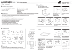
1
For Technology
in Quality
User's Manual
TQM5200
TQM5200 UM 300
12.10.2010
User's Manual TQM5200 UM 300
Table of contents
1.
ABOUT THIS MANUAL ............................................................................................................... 7
1.1
1.2
1.3
1.4
1.5
1.6
1.7
Tips on Safety ................................................................................................................ 7
Terms and Conventions ................................................................................................. 7
Handling and ESD tips ................................................................................................... 8
Registered Trademarks .................................................................................................. 9
Imprint ............................................................................................................................ 9
Copyright ........................................................................................................................ 9
Disclaimer....................................................................................................................... 9
2.
PRODUCT IDEA...................................................................................................................... 10
3.
FUNCTIONALITY AND SYSTEM ARCHITECTURE........................................................................ 10
4.
System Architecture / Block Diagram ........................................................................... 10
System Components .................................................................................................... 11
ELECTRONICS SPECIFICATION ............................................................................................... 12
4.1
System components ..................................................................................................... 12
4.1.1
CPU ....................................................................................................................... 12
4.1.2
CPU-Power-On Reset Configuration ..................................................................... 14
4.1.3
CPU-Clock generation ........................................................................................... 16
4.1.4
CPLD ..................................................................................................................... 18
4.1.5
Temperature Monitoring......................................................................................... 18
4.1.6
Address Register ................................................................................................... 19
4.1.7
Bus Driver .............................................................................................................. 19
4.1.8
Flash Memory ........................................................................................................ 19
4.1.9
SRAM..................................................................................................................... 22
4.1.10 EEPROM ............................................................................................................... 23
4.1.11 SDRAM .................................................................................................................. 23
4.1.11.1 Parameter for SDRAM-Controller Configuration ............................................ 24
4.1.11.2 SDRAM components ..................................................................................... 24
4.1.12 Graphics Controller ................................................................................................ 25
4.1.13 Clock generation for Graphics Controller............................................................... 27
4.1.14 Diagnosis-LED ....................................................................................................... 27
4.1.15 Serial Interfaces ..................................................................................................... 27
4.1.16 Module Interfaces .................................................................................................. 28
4.1.16.1 Board-to-Board Connectors ........................................................................... 28
4.1.16.2 Plug Connector X1 ......................................................................................... 29
4.1.16.3 Pin Configuration X1 ...................................................................................... 31
4.1.16.4 Plug Connector X3 ......................................................................................... 32
4.1.16.5 Pin Configuration X3 ...................................................................................... 34
4.1.16.6 Pin Configuration X2 ...................................................................................... 35
4.1.16.7 Pin Configuration X4 ...................................................................................... 35
4.1.16.8 Electrical Characteristics of the Module Interfaces ........................................ 36
Page 2
©2010 by TQ-Components GmbH
3.1
3.2
User's Manual TQM5200 UM 300
Table of contents
4.1.17 Chip-Selects und Interrupts....................................................................................40
4.1.18 Service Interfaces...................................................................................................40
4.1.18.1 Download Interface ........................................................................................40
4.1.18.2 COP/JTAG Interface ......................................................................................40
4.1.19 Supply ....................................................................................................................41
4.1.19.1 Tolerance of the external supply voltage........................................................41
4.1.19.2 Internal voltage...............................................................................................41
4.1.19.3 Power Consumption Maximum Values ..........................................................42
4.1.19.4 Power Consumption, Typical Values..............................................................42
4.1.19.5 Reset-Logic / Supervisor ................................................................................42
©2010 by TQ-Components GmbH
5.
MECHANICS ...........................................................................................................................43
5.1
5.2
5.3
5.4
5.5
5.6
General Information ......................................................................................................43
Dimensions ...................................................................................................................43
Mounting .......................................................................................................................43
Top View TQM5200......................................................................................................44
Bottom View TQM5200.................................................................................................44
Side View TQM5200.....................................................................................................45
6.
SOFTWARE ............................................................................................................................45
7.
SAFETY REQUIREMENTS AND PROTECTIVE REGULATIONS ......................................................46
7.1
7.2
7.3
7.4
7.5
8.
EMC Requirements ......................................................................................................46
ESD Requirements .......................................................................................................46
Reliability and Service Life............................................................................................46
Climate Conditions and Operational Conditions ...........................................................47
Environmental Protection..............................................................................................47
APPENDIX .............................................................................................................................48
8.1
8.2
Acronyms and Definitions .............................................................................................48
References ...................................................................................................................50
Page 3
User's Manual TQM5200 UM 300
Illustration directory
Illustration 1:
Illustration 2:
Illustration 3:
Illustration 4:
Illustration 5:
Illustration 6:
Illustration 7:
Illustration 8:
Illustration 9:
Illustration 10:
Illustration 11:
Illustration 12:
TQM5200 Block Diagram................................................................................ 10
Processor Block Diagram ............................................................................... 12
MPC5200 Clock Relations .............................................................................. 17
Chip Select 0 / Boot Configuration Register—MBAR + 0x0300...................... 19
Chip Select 2 Configuration Register—MBAR + 0x0308 ................................ 22
SM501 Block Circuit Diagram ......................................................................... 25
Chip Select 1 Configuration Register—MBAR + 0x0304 ................................ 26
Supply voltage ................................................................................................ 41
Top view through the printed circuit board ...................................................... 43
Top View ......................................................................................................... 44
Bottom View.................................................................................................... 44
Stack heights (not to scale)............................................................................. 45
©2010 by TQ-Components GmbH
Page 4
User's Manual TQM5200 UM 300
©2010 by TQ-Components GmbH
Table directory
Table 1:
Table 2:
Table 3:
Table 4:
Table 5:
Table 6:
Table 7:
Table 8:
Table 9:
Table 10:
Table 11:
Table 12:
Table 13:
Table 14:
Table 15:
Table 16:
Table 17:
Table 18:
Table 19:
Table 20:
Table 21:
Table 22:
Table 23:
Table 24:
Table 25:
Table 26:
Table 27:
Table 28:
Table 29:
Table 30:
Table 31:
Table 32:
Table 33:
Table 34:
Terms and conventions..........................................................................................7
CPU .....................................................................................................................14
Reset Configuration .............................................................................................15
Oscillators and crystal oscillator for the MPC5200 ..............................................16
CPLD ...................................................................................................................18
TQM5200 CPLD-JTAG-Interface.........................................................................18
Temperature Sensor ............................................................................................18
Address Register .................................................................................................19
Bus Driver ............................................................................................................19
Chip Select 0 / Boot Configuration Register ........................................................21
Flash-Memory component ...................................................................................21
Chip Select 2 Configuration Register...................................................................22
SRAM Memory component..................................................................................22
Serial EEPROM ...................................................................................................23
Parameter for SDRAM-Controller Configuration..................................................24
SDRAM components (selection of all released components) ..............................24
Graphics Controller ..............................................................................................26
Chip Select 1 Configuration Register...................................................................26
Oscillators for the Graphics Controller .................................................................27
RS232 / UART Signals ........................................................................................27
RS232 Transceiver ..............................................................................................27
Board-to-Board Connectors .................................................................................28
Plug Connector X1...............................................................................................30
Pin configuration plug connector X1 (base module connector 1) ........................31
Plug Connector X3...............................................................................................33
Pin configuration plug connector X3 (base module connector 2) ........................34
Pin Assignment Connector X2 (Graphics Connector 1).......................................35
Pin Assignment Connector X4 (Graphics Connector 2).......................................35
Signal Characteristics ..........................................................................................39
Available Chip Selects and Interrupts ..................................................................40
COP/JTAG-Interface............................................................................................40
Maximum current consumption............................................................................42
Stack Heights.......................................................................................................45
Acronyms and Definitions ....................................................................................49
Page 5
User's Manual TQM5200 UM 300
Revision history
Rev.
Date
Name
Pos.
Modification
049
08.08.2004
VJU
Creation (Provisional Specification)
050
09.08.2004
ANW
Adaptation
201
17.01.2005
VJU
Finalization
202
16.02.2005
VJU
Revision after internal checks
203
25.02.2005
VJU
14.04.2005
ANW
Revision
204
10.05.2005
DEN
Translation
300
12.10.2010
F. Petz
Completely revised
5.3
Drawing added
©2010 by TQ-Components GmbH
Page 6
User's Manual TQM5200 UM 300
1. About this manual
This manual contains technical information concerning the TQ-Minimodule TQM5200.
1.1 Tips on Safety
Improper or incorrect handling of the product can substantially reduce its life span.
1.2 Terms and Conventions
Symbol / Tag
Meaning
This symbol represents the handling of electrostatic-sensitive modules and / or
components. These components are often damaged / destroyed with the
transmission of a voltage higher than about 50 V. A human body usually only
experiences electrostatic discharges above approximately 3,000 V.
©2010 by TQ-Components GmbH
This symbol indicates the possible use of voltages greater than 24 V. Please
note the relevant statutory regulations in this regard. Non-compliance with
these regulations can lead to serious damage to your health and also cause
damage / destruction of the component.
This symbol indicates a possible source of danger. Acting against the
procedure described can lead to possible damage to your health and / or
cause damage / destruction of the material used.
This symbol represents important details or aspects for working with TQproducts.
Filename.ext
This specification is used to state the complete file name with its
corresponding extension.
Examples of an application. e.g.,
Instructions /
Examples
Reference
Table 1:
•
•
•
Specifying memory partitions
Processing a script
..............................
Cross-reference to another section, figure or table.
Terms and conventions
Page 7
User's Manual TQM5200 UM 300
1.3 Handling and ESD tips
General handling of your TQ-products
The TQ-product may only be used and serviced by certified personnel who have
taken note of the information, the safety regulations in this document and all related
rules and regulations.
A general rule is: not to touch the TQ-product during operation. This is especially
important when switching on, changing jumper settings or connecting other devices
without ensuring beforehand that the system’s power supply is switched off.
Violation of this guideline may result in damage / destruction of the module and be
dangerous to your health.
Improper handling of your TQ-product renders the guarantee invalid.
Proper ESD handling
Always wear antistatic clothing and use ESD-safe tools, packing materials etc. and
operate your TQ-product in an ESD-safe environment. Especially when you switch
modules on, change jumper settings, or connect other devices.
Page 8
©2010 by TQ-Components GmbH
The electronic components of your TQ-product are sensitive to electrostatic
discharge (ESD).
User's Manual TQM5200 UM 300
1.4 Registered Trademarks
TQ-Components GmbH aims to adhere to the copyrights of all the used graphics and texts in
all publications and strives to use original or license-free graphics and texts.
All the brand names and trademarks mentioned in the publication, including those protected
by a third party, unless specified otherwise in writing, are subjected to the specifications of
the current copyright laws and the proprietary laws of the present registered proprietor
without any limitation. One should conclude that brands and trademarks are protected
through the rights of a third party.
1.5 Imprint
©2010 by TQ-Components GmbH
TQ-Components GmbH
Gut Delling, Mühlstraße 2
D–82229 Seefeld
Tel.:
+49 (0)8153 9308-0
Fax:
+49 (0)8153 9308-134
Email: [email protected]
Web:
http://www.tq-components.com
1.6 Copyright
Copyright protected © 2010 by TQ-Components GmbH.
This manual may not be copied, reproduced, translated, changed or distributed, completely
or partially in electronic, machine readable, or in any other form without the written consent of
TQ-Components GmbH.
1.7 Disclaimer
TQ-Components GmbH does not guarantee that the information in this manual is up-to-date,
correct, complete or of good quality. Nor does TQ-Components assume guarantee for further
usage of the information. Liability claims against TQ-Components GmbH, referring to
material or idea related damages, caused due to usage or non-usage of the information
given in the manual, or caused due to usage of erroneous or incomplete information, are
exempted, as long as there is no proven, intentional or negligent fault of TQ-Components
GmbH.
TQ-Components GmbH explicitly reserves the rights to change or add to the contents of this
manual or parts of it without special notification.
Page 9
User's Manual TQM5200 UM 300
2. Product Idea
While designing the TQM5200, particular importance has been given to the compact
dimensions. With just 80 × 60 mm², the TQM5200 has a very compact form factor.
Apart from requiring less space on the target hardware, it also has advantages with
mechanical stress, e.g. shock or vibration. Robustness and industrial suitability were also
important criteria according to which the connector system of the module was selected.
Based on experience, a 0.8 mm mezzanine connector system is used.
3. Functionality and System Architecture
The TQM5200 is a Minimodule based on the MPC5200 PowerPC-CPU (Freescale) and an
SM501 graphics controller by Silicon Motion.
3.1 System Architecture / Block Diagram
SDRAM
32 Bit
3,3 V
16MByte ... 128MByte
(256MByte)
Supervisor
3,3V Power-Fail-Logic
SRAM Battery Backup
Core Supply
1,5 V
SRAM
EEPROM
Oszillator
33MHz
Reset
Configuration
PLD
Programmable
Serial
Controllers
SDRAM
Controller
including
Motorola PowerPC MPC5200
400MHz
Ethernet10/100,
USB-Host, UART,
I2C, SPI, IRDA,
CAN, AC97,
Codec
Supervisor
1,5V
Power-Fail-Logic
16 Bit multiplexed
seriell (I2C)
0/ 1kBit ... 64kBit
PCI-Bus
66MHz / 33MHz
Local-Plus-Bus
0KByte / 512kByte / 1MByte
(battery backup)
AdressRegister
24 Bit
Flash
32 Bit multiplexed
4MByte ... 32MByte (64MByte)
66MHz / 33MHz
PowerFail-Logic
ATA-Bus
BusTreiber
32 Bit
Oscillator
24MHz
Cope
Supply
1,8V
COP / JTAG
RS232
Grafik Controller
(32 Bit multiplexed)
Test / Degugging
Drivers for 2*RS232
SM501
8MB Byte internal Memory
240 Pin Basis Board to Board Connector
0,8 mm Pitch
Illustration 1:
TQM5200 Block Diagram
Page 10
80 Pin Grafik Board to Board
Connector
0,8 mm Pitch
©2010 by TQ-Components GmbH
External Power Supply
User's Manual TQM5200 UM 300
3.2 System Components
The board contains the following system components:
©2010 by TQ-Components GmbH
•
•
•
•
•
•
•
•
•
•
•
•
•
•
•
•
•
•
•
Freescale PowerPC processor MPC5200B up to 400 MHz with MPC603e processor core
33 MHz oscillator for the CPU clock
Silicon Motion graphics controller SM501 with 8 Mbyte internal graphics memory
24 MHz oscillator for the graphics controller
SDRAM: 16 Mbyte up to 128 Mbyte 1 / 256 Mbyte 2 ; 32 bit data bus width
Flash: 4 Mbyte up to 32 Mbyte Flash 3 , 32 bit data bus width
SRAM: no SRAM, 512 Kbyte or 1 Mbyte, 16 bit data bus width.
Possibility for battery back-up via battery supply from the target hardware
Serial EEPROM: 0 kbit or 64 kbit, I²C bus
CPLD for Reset-Configuration and control of SRAM and graphics controller
Driver for two serial interfaces (RxD, TxD)
32 bit bus driver and 24 bit address register for module components at the Local-Plus-Bus
COP/JTAG interface
Single power supply 3.3 V
Switch-mode DC/DC converter on-board (3.3 V to 1.5 V)
Linear DC/DC converter on-board (3.3 V to 1.8 V)
1.5 V supervisor / power-fail logic
1.8 V supervisor / power-fail logic
3.3 V supervisor / power-fail logic with SRAM battery backup
240 pin + 80 pin (320 pin) Board-to-Board plug system
All pins of the PowerPC processors are routed to the two 120 pin Board-to-Board connectors,
except the SDRAM interface and the XTAL pins. Further, all pins of the graphics controller
related to the LCD and CRT interface are routed to two 40 pin module connectors.
Transceivers for Ethernet, USB, CAN, etc… (except RS232 transceivers), are not assembled
on the module. If necessary, drivers can be implemented on the target hardware.
1
2
3
With one memory bank for the MPC5200 Rev 1.2 (Chip masks Revision A)
With two memory banks starting with MPC5200 Chip masks Revision B (from Q3/2005)
64 and128 Mbyte addressed by the bank-select bits
Page 11
User's Manual TQM5200 UM 300
4. Electronics Specification
The module is supplied with 3.3 V DC. The processor core voltage (1.5 V) and the core
voltage for the graphics controller (1.8 V) are generated from the input voltage (3.3 V) on the
module with voltage regulators.
The TQM5200 is specified for a temperature range of 0 °C to +70 °C.
Optionally it is also available for a temperature range of –40 °C to +85 °C.
4.1
System components
4.1.1
CPU
©2010 by TQ-Components GmbH
Illustration 2:
Processor Block Diagram
Page 12
User's Manual TQM5200 UM 300
The module offers the following features:
CPU Core
•
•
•
•
•
•
•
•
MPC603e series G2_LE core
Superscalar architecture
760 MIPS at 400 MHz (–40 °C to +85 °C)
450 MIPS at 264 MHz (–40 °C to +105 °C)
16 k Instruction cache, 16 k Data cache
Double precision FPU
Instruction and Data MMU
Standard & Critical interrupt capability
SDRAM Memory Interface
•
•
•
•
Up to 133 MHz operation
256 Mbyte addressing range
32 bit data bus
Built-in initialization and refresh
External Bus Interface
©2010 by TQ-Components GmbH
•
•
•
•
•
Supports interfacing to ROM/Flash/SRAM memories or other memory mapped devices
8 programmable Chip Selects
Non multiplexed data access using 8/16/32 bit data bus with up to 26 bit address
Short or Long Burst capable
Multiplexed data access using 8/16/32 bit data bus with up to 25 bit address
Peripheral Component Interconnect (PCI) Controller
•
•
•
•
•
Version 2.2 PCI compatibility
PCI initiator and target operation
32 bit PCI address / data bus
33 and 66 MHz operation
PCI arbitration function
ATA Controller
•
•
Version 4 ATA compatible external interface
ATA Software Reset via PSC1.4.
If this feature is used, do not use PSC1.4 for other functions
Six Programmable Serial Controllers (PSCs)
•
•
•
•
UART or RS232 interface
CODEC interface for Soft Modem, Master/Slave CODEC Mode, I2S and AC97
Full duplex SPI mode
IrDA mode from 2400 bps to 4 Mbps
Fast Ethernet Controller (FEC)
•
Supports 100 Mbps IEEE 802.3 MII, 10 Mbps IEEE 802.3 MII, 10 Mbps 7-wire interface
Universal Serial Bus Controller (USB)
•
•
Version 1.1 Host only
Support for two independent USB slave ports
Two Inter-Integrated Circuit Interfaces (I²C)
Serial Peripheral Interface (SPI)
Dual CAN 2.0 A/B Controller (MSCAN)
•
•
•
Motorola Scalable Controller Area Network (MSCAN) architecture
Implementation of version 2.0A/B CAN protocol
Standard and extended data frames
J1850 Byte Data Link Controller (BDLC)
•
•
•
J1850 Class B data communication network interface compatible and ISO compatible
for low speed (<125 kbps) serial data communications in automotive applications
Supports 4× mode, 41.6 kbps
In-frame response (IFR) types 0, 1, 2, and 3 supported
Page 13
User's Manual TQM5200 UM 300
Component
MPC5200CVR400B
Table 2:
Manufacturer
Freescale
Type
400 MHz PPC
Temperature Range
–40 °C to +85 °C
CPU
The functions described here are not available simultaneously. The
PSCs functions are multiplexed. More information about it can be
found in section 2 of the MPC5200 User-Manual.
4.1.2
CPU-Power-On Reset Configuration
Page 14
©2010 by TQ-Components GmbH
In the table shown below, the described adjustments are made as per the rising edges of
HRESET# and a Hold-Time of two clock cycles (SYS_XTAL) of CPU pins; and are stored in
the CDM Reset Configuration register. The adjusted configuration cannot be changed when
the CPU is running.
The Reset configuration is set by a CPLD. During the Reset phase, the configuration is set at
the configuration pins of the CPU until the rising edge of the HRESET#. Afterwards the CPLD
outputs are changed to high impedance. Wrong adjustment can render the system to be no
longer bootable.
With the settings established, the PLL configuration is among the things that are of concern.
This configuration determines the XL bus Frequency and the CPU core frequency. Settings
for PCI and Local-Plus-Bus are derived from the XL bus frequency and can be changed at
runtime. Further boot settings are made here, which apply only to data accesses over BootCS#. The access over Boot-CS0# to CS5# can be changed at runtime.
Warning! The default values specified in Table 3 are qualified for the module TQM5200. The
settings of the deviating values takes place at one’s own risk and without guarantee on the
part of TQ Components GmbH. Malfunctions as well as destruction of the module cannot be
excluded with deviating configurations.
User's Manual TQM5200 UM 300
Reset
TQM5200
Config
Start-up
Pin
Config.
RST_CFGx
CDM
Reset
Config
Register
Bit
I/O Signal
Name
Config Signal
from CDM
Description
©2010 by TQ-Components GmbH
PORCFG[x]
0
0
31
ATA_DACK#
ppc_pll_cfg_4
1
0
30
ATA_IOR#
ppc_pll_cfg_3
2
0
29
ATA_IOW#
ppc_pll_cfg_2
3
1
28
LP_RW
ppc_pll_cfg_1
4
0
27
LP_ALE#
ppc_pll_cfg_0
5
0
26
LP_TS#
xlb_clk_sel
Bit=0: XLB_CLK=SYS_PLL FVCO/4
Bit=1: XLB_CLK=SYS_PLL FVCO/8
6
0
25
USB1_1
sys_pll_cfg_0
Bit=0:
Bit=1:
7
0
24
USB1_2
sys_pll_cfg_1
Bit=0: VCO = SYS_PLL_VCO
Bit=1: VCO = 2 × SYS_PLL_FVCO
8
0
23
ETH0
boot_rom_mg
Bit=0: No Boot in Most Graphics Mode
Bit=1: Boot in Most Graphics Mode
MPC5200 G2_LE PPC
Core PLL Configuration
SYS_PLL FVCO=16 × SYS_PLL_FREF
SYS_PLL FVCO=12 × SYS_PLL_FREF
10
0
21
ETH2
ppc_msrip
Microprocessor Boot Address/Exception
table location
Bit=0: 0000_0100 (hex)
Bit=1: FFF0_0100 (hex)
11
1
20
ETH3
boot_rom_wait
Bit=0: 4 IP bus clocks of wait state
Bit=1: 48 IP bus clocks of wait state
ETH4
Bit=0: No byte lane swap,
same endian ROM image
boot_rom_swap
Bit=1: Byte lane swap,
different endian ROM image
12
0
19
For non-muxed boot ROMs:
Bit=0: 8 bit boot ROM data bus, 24 bit
max boot ROM address bus
Bit=1: 16 bit boot ROM data bus,16 bit
boot ROM address bus
13
1
18
ETH5
boot_rom_size
For muxed boot ROMs:
boot ROM address is max 25 significant
bits during address tenure.
Bit=0: 16 bit ROM data bus
Bit=1: 32 bit ROM data bus
14
1
17
ETH6
boot_rom_type
Bit=0: non-muxed boot ROM bus,
single tenure transfer.
Bit=1: muxed boot ROM bus, with
address and data tenures,
ALE and TS active
15
0
16
ETH1
large_flash_sel
Bit=0: No Boot in Large Flash Mode
Bit=1: Boot in Large Flash Mode
Table 3:
Reset Configuration
Page 15
User's Manual TQM5200 UM 300
4.1.3
CPU-Clock generation
On the module two oscillators and one crystal oscillator are present.
• 33 MHz oscillator for the CPU
• 24 MHz oscillator for the SM501 Graphics controller
• 32.768 kHz crystal oscillator for the MPC5200’s RTC
To use this RTC, the 3.3 V supply voltage of the module must be available. In order to
reduce the quiescent current input for a system, it is recommended to implement an external
RTC on the target hardware. An external RTC can be connected e.g. via the I²C bus.
All clock frequencies required by the CPU are generated CPU-internal derived from the
33 MHz oscillator.
Component
Manufacturer
Type
Temperature Range
TJE
Oscillator, 33 MHz
–40 °C to +85 °C
SX03-0507-E-50-W24.000MHz
TJE
Oscillator, 24 MHz
–40 °C to +85 °C
MC306
Epson / Seico
Crystal oscillator
32.768 kHz
–40 °C to +85 °C
Table 4:
Oscillators and crystal oscillator for the MPC5200
The clock frequencies for the TQM5200 module are derived from the 33 MHz input clock and
set by the Reset configuration register to generate the following frequencies:
•
•
•
•
XLB-Clk:
IPB-Clk:
PCI-Bus-Clk:
Core-Clk:
132 MHz
132 MHz
66 MHz
396 MHz
Page 16
©2010 by TQ-Components GmbH
SX03-0507-E-50-W33.000MHz
©2010 by TQ-Components GmbH
User's Manual TQM5200 UM 300
Illustration 3:
MPC5200 Clock Relations
Page 17
User's Manual TQM5200 UM 300
4.1.4
CPLD
A Lattice ispMach4064V 5T48I is used as CPLD in a 48 pin TQFP housing.
In addition to the CPU-Power-On Reset Configuration described above, the CPLD generates
two Byte-Select signals for the SRAM.
Component
Manufacturer
ispMach4064V 5T48I
Table 5:
Type
Lattice
Temp. range
CPLD 64 macro cells
–40 °C to +85 °C
CPLD
The JTAG pins of the CPLD are connected to the module pins of the TQM5200 described in
the following table.
Signal
Module-Pin
Direction
Description
X3-118
I
CPLD-JTAG-Interface
TDI_PLD
X3-115
I
CPLD-JTAG-Interface
TDO_PLD
X3-116
O
CPLD-JTAG-Interface
TMS_PLD
X3-117
I
CPLD-JTAG-Interface
DVCC3V3
VCC3V3
–
Supply
GND
–
Ground
DGNDG
Table 6:
4.1.5
TQM5200 CPLD-JTAG-Interface
Temperature Monitoring
•
•
•
Monitors the CPU temperature indirectly, using a temperature sensor on the soldering
side of the PCB near the CPU
Sensor LM75
The switching output of LM75 is routed to the Board-to-Board connectors
Control via I²C bus (I2C_2SCL / I2C_2SDA); address lines on 0b000; I²C bus is shared with
the EEPROMs as the address parts are fixed and there is no address collision with
EEPROMs.
Component
LM75CIMM-3
Table 7:
Manufacturer
National
Semiconductor
Model
I²C, 400 kHz, 3 Addr.,
MSOP8 (0.65 mm)
Temperature Sensor
Page 18
Temperature Range
–40 °C to +85 °C
©2010 by TQ-Components GmbH
TCK_PLD
User's Manual TQM5200 UM 300
4.1.6
Address Register
All bus subscribers which are connected to the Local-Plus-Bus in multiplexed mode (SRAM,
flash, graphics controller) require an address register with up to 25 bit width. The addresses
are locked with the address register with the rising edge of the inverted LP_ALE# signal.
As a latch the positive edge triggered register 74LVC16374 is used.
Component
SN74LVC16374 DGG
Table 8:
4.1.7
Manufacturer
TI
Model
16 bit D-Latch
Temperature Range
–40 °C to +85 °C
Address Register
Bus Driver
©2010 by TQ-Components GmbH
Bus drivers are installed, to prevent a bus overload. This bus is divided into Local-Plus, ATA
and PCI bus. Two 16 bit bus drivers type 74ALVC16245A are used. The bus drivers are
activated with the signals Boot-CS#, CS0# (flash), CS1# (graphics controller) and CS2#
(SRAM). The change of direction is controlled by the LP_RW# signal.
Component
74ALVC16245A
Table 9:
4.1.8
Manufacturer
Philips
Model
16 bit bus driver
Temperature Range
–40 °C to +85 °C
Bus Driver
Flash Memory
•
•
•
3.3 V flash of the MirrorBit-Series (Samsung), 16 bit
1 bank with two devices and a bus width of 32 bit
Connected at the multiplexed Local-Plus-Bus. The address signals are connected via a
25 bit address register and the data is connected via a 32 bit bus driver
• The ALE# signal is configured as “long“
• Eight wait states are used for accessing the flash memory
• Memory sizes of 4 to 32 Mbyte, using the Bank-Select bits 64 / 128 Mbyte
• Access time 120 ns
• The signal Boot-CS# (physical CS0#) is used as chip select to boot from Flash.
The configuration for CS0 is described in Table 10.
The status signal RY/BY# of the Flash is not used, i.e. the write and delete cycles must be
checked by polling the Flash status bits (DQ7#, Toggle bits etc.).
Illustration 4:
Chip Select 0 / Boot Configuration Register—MBAR + 0x0300
Page 19
User's Manual TQM5200 UM 300
Chip Select 0 / Boot Configuration Register
Bits
Name
Setting
WaitP
0x00
8:15
WaitX
0x08
16
MX
1
17
AL
1
18
AA
0
19
CE
1
20:21
AS
11
22:23
DS
11
24:25
Bank
00
26:27
WTyp
11
Number of wait states to insert. Can be applied as a prescale to WaitX or used by itself, as specified by
WTyp bits below. Wait states control how many PCI clocks the corresponding CS pin remains active.
Base number of wait states to insert, or combined with WaitP as specified by WTyp bits below.
cfg operation—If rstcfg[11] (on pad_eth_03) is zero then 4 wait states are in effect, else 48 wait states
are in effect. Wait States equals the number of PCI clocks from CS assertion to when data must be valid
from boot device.
MX bit specifies whether a transaction operates as multiplexed or non-multiplexed.
A multiplexed transaction presents address and data in different tenures. During the address tenure, ALE
is asserted. At the end of ALE, AD bus is switched to data tenure and CSx pin is asserted.
0=Non-multiplexed
1=Multiplexed
cfg operation —If rstcfg[14] on pad_eth_06 is low, boot operation is non-multiplexed (single tenure), else
boot operation is multiplexed (dual tenure).
ALE length—multiplexed transactions only
0=ALE width is 1 internal IP bus clock
1=ALE width is 2 internal IP bus clocks
At boot time, internal IP bus clock is twice the frequency of the PCI clock. Therefore, AL defaults to 1 (2 IP
bus clocks) for boot device.
ACK Active—multiplexed transactions only. This bit defines whether ALE input is active or not. If AA is 1,
programmed wait states can be overridden when/if the external device drives the ACK input low. If AA is
0, the ACK input is ignored.
Wait states are still in effect. If no ACK is received, cycle terminates at end of wait state period.
cfg operation —If rstcfg[14] on pad_eth_06 is high, indicating multiplexed mode boot device, then AA is
assumed high as well. This lets the boot device shorten the Wait State period by asserting the ACK input.
An individual Enable bit—allows CS operation for the corresponding CS pin. CE must be high to allow
operation. Register 6 master enable bit must also be high, except when CS[0] is used for boot ROM.
1 = Enable
0 = Disabled, register writes can occur but no external access is generated.
Address Size field—defines size of peripheral Address bus (in bytes) and must be consistent with physical
connections.
00 = 8 bits
01 = 16 bits
10 = 24 bits
11 = > 25 bits
See documentation for Physical Connection requirements. The combination of address size, data size,
and transaction type (MX) must be consistent with the peripheral physical connection. In case of a
multiplexed transaction, the entire address is driven regardless of address size field.
cfg operation —If rstcfg[13] on pad_eth_05 is low, then the address size for non-multiplexed boot device
is set to 24 bits (AS=10), else the boot device is treated as a 16 bit address (AS=01) device. For
multiplexed mode boot devices the maximum 25 bits of address is always driven. This rstcfg bit more
particularly affects the DS field below, and can be thought of as the “small” or “big” data size config bit.
Data Size field—represents the peripheral data bus size (in bytes):
00=1 Byte
01=2 Bytes
10=3 Bytes (Not Supported)
11=4 Bytes
cfg operation—If rstcfg[13] on pad_eth_05 is low, then the data size for non-multiplexed boot device is
set to 8 bits (DS=00), else the boot device is treated as a 16 bit (DS=01) device. For multiplexed mode
boot device the selection is 16 bit data or 32 bit data respectively.
Bank bits—are reflected on external AD lines (AD[26:25]) during Address tenure of a multiplexed
transaction. Register bit 24 is the msb and appears on AD[26].
Wait state type bits—define the application of wait states contained in WaitP and WaitX fields, as follows:
00 = WaitX is applied to read and write cycles (WaitP is ignored).
01 = WaitX is applied to Read cycles, WaitP is applied to Write cycles.
10 = WaitX is applied to Reads, WaitP/WaitX (16 bit value) is applied to Writes.
11 = WaitP/Waitx (as a full 16 bit value) is applied to Reads and Writes.
Page 20
©2010 by TQ-Components GmbH
0:7
Description
User's Manual TQM5200 UM 300
©2010 by TQ-Components GmbH
Bits
Name
Setting
28
WS
0
29
RS
0
30
WO
0
31
RO
0
Table 10:
Write Swap bit—If high, Endian byte swapping occurs during writes to a peripheral.
• For 8 bit peripherals, this bit has no effect.
• For 16 bit peripherals, byte swapping can occur.
• For 32 bit peripherals (possible in MUXed mode only) byte swap can occur.
1 = swap
0 = NO swap
2-byte swap is AB to BA, 4-byte swap is ABCD to DCBA.
NOTE: Transactions at less than the defined port size (i.e.., data size) apply swap rules as above,
according to the current transaction size.
Read Swap bit—Same as WS, but swapping is done when reading data from a peripheral.
1 = swap
0 = NO swap
cfg operation—If rstcfg[12] on pad_eth_04 is low, data from the boot device is Endian swapped when
read. This only has effect for boot devices configured as 16- or 32 bit data size.
Write Only bit—If bit is high, the peripheral is treated as a write-only device. An attempted read access
results in a bus error (as dictated by Chip Select Control Register EBEE bit) and/or an interrupt (as
dictated by Chip Select Control Register IE bit). In any case, no transaction is presented to the peripheral.
A bus error means the internal cycle is terminated with a transfer error acknowledge (ips_xfr_err assertion
to IP bus, TEA assertion to XL bus).
Read Only bit—If bit is high, the peripheral is treated as a read-only device. An attempted write access
results in a bus error (as specified by Chip Select Control Register EBEE bit) and/or an interrupt (as
specified by Chip Select Control Register IE bit). In any case, no transaction is presented to the
peripheral.
NOTE: This bit is high from Reset, indicating Boot Device is Read-Only.
Chip Select 0 / Boot Configuration Register
Component
K8P2815UQB-EI4B
Table 11:
Description
Manufacturer
Samsung
Model
Flash MirrorBit, 16 M × 16
Temperature Range
–40 °C to +85 °C
Flash-Memory component
These devices have a 64-ball-Fortified-BGA housing with dimensions of 13 × 11 mm.
Page 21
User's Manual TQM5200 UM 300
4.1.9
SRAM
•
•
•
•
•
•
•
•
One memory bank with 16 bit bus width
Memory capacity 512 Kbyte or optional 1 Mbyte
Access time 70 ns
Battery buffering via module connector (Standby-Power consumption, max. 20 µA)
The SRAM is connected via an address register and a bus driver to the multiplexed
Local-Plus-Bus of the processor
The ALE#-Signal is configured as “long”
Four wait states are used for accessing the SRAM
Signal CS2# is used for SRAM selection
Chip Select 2 Configuration Register—MBAR + 0x0308
Bits
Name
Setting
0:7
8:15
16
17
18
19
20:21
22:23
24:25
26:27
28
29
30
31
WaitP
WaitX
MX
AL
AA
CE
AS
DS
Bank
Wtyp
WS
RS
WO
RO
0x00
0x04
1
1
0
1
11
01
00
11
0
0
0
0
Table 12:
Description
Number of Wait States
The base number of wait states
MX bit specifies whether transaction operates as multiplexed or non-multiplexed
ALE Length
ACK Active
Chip Enable bit
Address Size field
Data Size field
Bank bits
Wait state Type bits
Write Swap bit
Read Swap bit
Write Only bit
Read Only bit
Chip Select 2 Configuration Register
Component
Manufacturer
Type
Temperature Range
K6X4016T3F-TF70
Samsung
SRAM, 4 Mbit
–40 °C to +85 °C
K6X8016T3B-TF70
Samsung
SRAM, 8 Mbit
–40 °C to +85 °C
IS62WV25616BLL-55TLI
ISSI
SRAM, 4 Mbit
–40 °C to +85 °C
IS62WV51216BLL-55TLI
ISSI
SRAM, 8 Mbit
–40 °C to +85 °C
Table 13:
SRAM Memory component
Page 22
©2010 by TQ-Components GmbH
Illustration 5:
User's Manual TQM5200 UM 300
4.1.10 EEPROM
The serial EEPROM can e.g. store the characteristics of the module and customer specific
parameter data non-volatile. As against flash, individual memory cells can be deleted and
overwritten in the EEPROM. At delivery the EEPROM is erased.
©2010 by TQ-Components GmbH
•
•
•
•
0 to 64 Kbit
Control via I²C bus 2 of the CPU (I2C_2SCL / I2C_2SDA)
10 kΩ Pull-up resistors at I2C_2SCL and I2C_2SDA
Address lines of EEPROM at 0b000
Component
Manufacturer
M24C01WDW6
ST Microelectronics
1-K EEPROM / TSSOP8
–40 °C to +85 °C
M24C02WDW6
ST Microelectronics
2-K EEPROM / TSSOP8
–40 °C to +85 °C
M24C04WDW6
ST Microelectronics
4-K EEPROM / TSSOP8
–40 °C to +85 °C
M24C08WDW6
ST Microelectronics
8-K EEPROM / TSSOP8
–40 °C to +85 °C
M24C16WDW6
ST Microelectronics
16-K EEPROM / TSSOP8
–40 °C to +85 °C
M24C32WDW6
ST Microelectronics
32-K EEPROM / TSSOP8
–40 °C to +85 °C
M24C64WDW6
ST Microelectronics
64-K EEPROM / TSSOP8
–40 °C to +85 °C
Table 14:
Model
Temperature Range
Serial EEPROM
4.1.11 SDRAM
•
•
•
•
•
•
•
Up to four memory devices with a bus width of 16 bit each
Chip-Select through Mem_CS0 and Mem_CS1
132 MHz clock
One or two memory banks, each 32 bit wide
Available for normal temperature range: 16 Mbyte to 256 Mbyte
Available for extended temperature range: 16 Mbyte to 128 Mbyte
CAS Latency 3
When the mode-, control- and configuration register of the Micron 48LC16M16A2-75 SDRAM
are programmed the following parameters must be taken into consideration:
Page 23
User's Manual TQM5200 UM 300
4.1.11.1
Parameter for SDRAM-Controller Configuration
Description
Setting
Table 15:
SDR
132
3
5.4
0
15
20
66
64
7.8125
8192
Normal
Yes
No
Yes
Yes
A10
Drive except to read
0
No
No
No
Unit
–
MHz
Clock Cycles
ns
tCK
ns
ns
ns
ms
µs
–
–
–
–
–
–
–
–
–
–
–
–
Parameter for SDRAM-Controller Configuration
The following register settings result from the above described parameters:
• Mode Register (MBAR+0x0100)
Ö 0x008D0000
Ö 0xD14F0000
• Control Register (MBAR+0x0104)
Ö 0xD2322800
• Configuration Register 1 (MBAR+0x0108)
• Configuration Register 2 (MBAR+0x010C)
Ö 0x8AD70000
The description of the individual register bits can be found in section 8 SDRAM Memory
Controller of the MP5200 User Manual [2].
The SDRAM components are listed in the following table.
4.1.11.2
SDRAM components
Component
MT48LC32M16A2TG 75 (K4S511632M-TC75)
MT48LC16M16A2TG 75 (K4S561632E-TI75)
MT48LC8M16A2TG 75 (K4S281632E-TI75)
MT48LC4M16A2TG 75 (K4S641632E-TI75)
Table 16:
Manufacturer
Model
SDRAM, 32 M × 16
SDRAM, 16 M × 16
SDRAM, 8 M × 16
SDRAM, 4 M × 16
Micron
Micron
Micron
Micron
Temperature Range
0 °C to +70 °C
–40 °C to +85 °C
–40 °C to +85 °C
–40 °C to +85 °C
SDRAM components (selection of all released components)
Page 24
©2010 by TQ-Components GmbH
Memory type
XLB Speed
CAS (Read) Latency
THZ
TDQSSmin
TWR
TRCD
TRFC
TREF
TREFI
#ROWs
Mode Register Type
Generate a Mode Register Set command
Self Refresh Mode
Automatic Refresh
Extend Row and Column
Precharge Control
Drive Rule for MDQ and MDQS
MDQS OE Mask
Mode Register Locked
Soft Refresh
Soft Precharge All
User's Manual TQM5200 UM 300
4.1.12 Graphics Controller
The Silicon Motion graphics controller SM501 is used.
Illustration 6:
SM501 Block Circuit Diagram
©2010 by TQ-Components GmbH
The SM501 offers the following features:
Host Interface
• Direct 32 bit CPU and PCI interface
• Xscale (PXA-25x), IXP4XX, SH3/4, and MIPS direct CPU bus interface
• PCI v2.1 compliant
Display Support
• LCD (digital) and CRT (analog) with Dual Display
• LCD: 320×240 up to 1024×768, 16/32 bit; 1280×1024 (16 bit only)
• CRT: VGA to SXGA, 16/32 bit
• Widescreen support up to 1280×768×16
• Hardware rotation
• Portrait and landscape display
• Can display different orientation on each output
2D/Video Acceleration Engine
• Optimized 128 bit 2D drawing engine
• Intelligent DMA command interpreter for enhanced performance
• Both front-end and back-end video engines
• 7 hardware display layers to support split screen, overlay, and alpha blending
• Per-pixel or planar alpha blend capability between layers
• Colour space conversion from: YUV422 (YUY2 and UYVY),YUV420 (Planar4:1:1),
YV12, IYUV (I420), IMC1, IMC2, IMC3, IMC4, NV12, NV21, RGB565, and RGBA888
to: RGB565 or RGBF888
Memory Configurations
• Dedicated graphics memory with 8 Mbyte
Package
• 19 mm × 19 mm, 297 pin BGA (0.8 mm ball grid)
• Process: 0.18 µm
• Internal memory option 0 or 8 Mbyte
Page 25
User's Manual TQM5200 UM 300
Component
SM501GE08
Table 17:
Manufacturer
Silicon Motion
Model
Graphics Controller
Temperature Range
–40 °C to +85 °C
Graphics Controller
The graphics controller operates at 66 MHz in the SH4 mode. For this, it is connected to the
Local-Plus-Bus of the MPC5200. The Local-Plus-Bus is selected in the memory by the CS1#
signals through the graphics controller and is configured as a 32 bit multiplexed bus.
The ALE# and the TS#-Signal are configured as “long”.
Access to the SM501 is controlled by acknowledge. Maximum number of wait states are
programmed for this type of access and for the addresses of CS1# signals. An access-cycle
ends one pulse after the falling edge of the acknowledge-signal.
The values for the CS1# Configuration Register are listed in the following table.
Bits
Chip Select 1 Configuration Register—MBAR + 0x0304
Name Setting*
Description
0:7
WaitP
0xff
Number of Wait States
8:15
WaitX
0xff
The base number of wait states
16
MX
1
MX bit specifies whether transaction operates as multiplexed or non-multiplexed
17
AL
1
ALE Length
18
AA
1
ACK Active
19
CE
1
Chip Enable bit
20:21 AS
11
Address Size field
22:23 DS
11
Data Size field
24:25 Bank
11
Bank bits
26:27 Type
11
Wait state Type bits
28
WS
0
Write Swap bit
29
RS
0
Read Swap bit
30
WO
0
Write Only bit
31
RO
0
Read Only bit
* Description of the setting as in Chip Select 0 Table 10
Table 18:
Chip Select 1 Configuration Register
Page 26
©2010 by TQ-Components GmbH
Illustration 7:
User's Manual TQM5200 UM 300
4.1.13 Clock generation for Graphics Controller
For clock generation a 24 MHz oscillator is mounted.
For applications with a TFT-Display on the Flat panel interface, a Low EMI Spread Spectrum
Oscillator is optionally installed. This is an interface, where heavy demands are made on the
electromagnetic interfering radiation.
Component
Manufacturer
Model
Temperature Range
SX03-0507-E-50-W-24.000MHz
TJE
Oscillator, 24 MHz
–40 °C to +85 °C
3HM57-F-24.000R-C1.5
EuroQuartz
Low EMI Spread Spectrum
Oscillator 24 MHz
–40 °C to +85 °C
Table 19:
Oscillators for the Graphics Controller
4.1.14 Diagnosis-LED
©2010 by TQ-Components GmbH
A red LED is provided to indicate CPU-Reset.
4.1.15 Serial Interfaces
The internal UART PSC1 or optional the UART PSC6 of the MPC5200B is connected via an
RS232-compatible transceiver (RxD / TxD channel) to the Board-to-Board connector.
It is configurable by placing 0 Ω resistors, irrespective of which of the two UARTs is used.
The internal UART PSC3 is connected via the RS232 transceiver to the Board-to-Board
connector (RxD / TxD channel). Optionally the PSC3 UART can be detached by removing
two 0 Ω resistors. The RS-232 interfaces offer a maximum speed of 115200 Baud.
RS232
Signal Name
RS232_TxD_1
RS232_RxD_1
RS232_TxD_2
RS232_RxD_2
Table 20:
Table 21:
Connector
X3-72
X3-71
X3-76
X3-75
Signal Name
UART1_TXD
UART1_RXD
UART3_TXD
UART3_RXD
CPU-Port
PSC1_0
PSC1_1
PSC3_0
PSC3_1
Connector
X3-65
X3-63
X3-53
X3-51
RS232 / UART Signals
Component
SP3222EEA
UART
Manufacturer
Sipex
Type
Dual RS232 transceiver
RS232 Transceiver
Page 27
Temperature Range
–40 °C to +85 °C
User's Manual TQM5200 UM 300
4.1.16 Module Interfaces
Except the SDRAM-interface, the PLL supply and the XTAL pins, all other microprocessor
pins are routed to the plug connectors. The CRT interface, the LCD interface as well as the
GPIOs of the graphics controller are routed to the plug connectors. Moreover, a MasterReset input, an SRAM backup power input as well as driven RxD- und TxD signals of the
RS232 interfaces are available at the module connectors.
The signals are allocated on the connector in such a manner that all processor signals, nonCPU and PLD signals as well as the reserve pins are routed to two 120 pin connectors.
The signals of the graphics controller are routed to two 40 pin module connectors.
4.1.16.1
Board-to-Board Connectors
Board-to-Board connection with two 120 pin and two 40 pin plug connectors, 0.8 mm pitch.
The 0.8 mm pitch plug connectors are available in different heights.
5 mm high module plug connectors are used on the TQM5200.
No. of Pins
5 mm
40
Qty Supplier
Supplier
Order No.
177984-1
6 mm
40
tyco
179029-1
7 mm
40
tyco
179030-1
8 mm
40
tyco
179031-1
120
tyco
177984-5
6 mm
120
tyco
179029-5
7 mm
120
tyco
179030-5
8 mm
120
tyco
179031-5
Table 22:
2
tyco
177983-1
No. of Pins
tyco
120
tyco
Order No.
40
5 mm
2
Target Hardware Connector
177983-5
Board-to-Board Connectors
The following lists describe the functionality and signal characteristics of the module pins:
Page 28
©2010 by TQ-Components GmbH
Module Connector
Board-toBoard
Distance
User's Manual TQM5200 UM 300
4.1.16.2
©2010 by TQ-Components GmbH
Pin
1
2
3
4
5
6
7
8
9
10
11
12
13
14
15
16
17
18
19
20
21
22
23
24
25
26
27
28
29
30
31
32
33
34
35
36
37
38
39
40
41
42
43
44
45
46
47
48
49
50
51
52
53
54
55
56
57
58
59
60
61
62
63
64
Plug Connector X1
Function
3V3
GND
ETH_17
ETH_16
ETH_15
ETH_14
ETH_13
ETH_12
ETH_11
GND
ETH_9
ETH_10
3V3
ETH_8
ETH_7
ETH_6
ETH_5
GND
ETH_3
ETH_4
ETH_1
ETH_2
IRQ3
ETH_0
3V3
GND
IRQ1
IRQ2
PCI_STOP#
IRQ0
PCI_RESET#
PCI_TRDY#
PCI_PERR#
GND
PCI_IRDY#
PCI_SERR#
3V3
PCI_REQ#
PCI_GNT#
PCI_PAR
PCI_DEVSEL#
GND
PCI_CBE_3#
PCI_ID_SEL
PCI_CBE_2#
PCI_FRAME#
PCI_CBE_1#
PCI_CLOCK
3V3
GND
PCI_CBE_0#
EXT_AD_30
EXT_AD_31
EXT_AD_28
EXT_AD_29
EXT_AD_26
EXT_AD_27
GND
EXT_AD_25
EXT_AD_24
3.3 V
EXT_AD_22
EXT_AD_23
EXT_AD_20
I/O Type1
PWR
PWR
I/O3V3, 4/4 mA
I/O3V3, 4/4 mA
I/O3V3, 4/4 mA
I/O3V3, 4/4 mA
I/O3V3, 4/4 mA
I/O3V3, 4/4 mA
I/O3V3, 4/4 mA
PWR
I/O3V3, 4/4 mA
I/O3V3, 4/4 mA
PWR
I/O3V3, 4/4 mA
I/O3V3, 4/4 mA
I/O3V3, 4/4 mA
I/O3V3, 4/4 mA
PWR
I/O3V3, 4/4 mA
I/O3V3, 4/4 mA
I/O3V3, 4/4 mA
I/O3V3, 4/4 mA
I/O 3V3, 4/4 mA, 100k PD
I/O 3V3, 4/4 mA, 100k PU
PWR
PWR
I/O 3V3, 4/4 mA, 100k PU
I/O 3V3, 4/4 mA, 100k PD
I/O 3V3, 16/16 mA, 5k6 PU
I/O 3V3, 4/4 mA, 100k PU
I/O 3V3, 16/16 mA, 5k6 PU
I/O 3V3, 16/16 mA, 5k6 PU
I/O 3V3, 16/16 mA, 5k6 PU
PWR
I/O 3V3, 16/16 mA, 5k6 PU
I/O 3V3, 16/16 mA, 5k6 PU
PWR
I/O 3V3, 8/8 mA, 5k6 PU
I/O 3V3, 8/8 mA
I/O 3V3, 16/16 mA
I/O 3V3, 16/16 mA, 5k6 PU
PWR
I/O 3V3, 16/16 mA
I/O 3V3, 8/8 mA
I/O 3V3, 16/16 mA
I/O 3V3, 16/16 mA, 5k6 PU
I/O 3V3, 16/16 mA
O 3V3, 12/12 mA
PWR
PWR
I/O 3V3, 16/16 mA
I/O 3V3, 10/10 mA
I/O 3V3, 10/10 mA
I/O 3V3, 10/10 mA
I/O 3V3, 10/10 mA
I/O 3V3, 10/10 mA
I/O 3V3, 10/10 mA
PWR
I/O 3V3, 10/10 mA
I/O 3V3, 10/10 mA
PWR
I/O 3V3, 10/10 mA
I/O 3V3, 10/10 mA
I/O 3V3, 10/10 mA
Description2
Module supply 3.3 V ±5 %
Module supply
CD / CRS
USB_OVRCNT / CTS / RX_ER
USB_RXN / RX / RXD[3]
USB_RXP / UART_RX / RXD[2]
USB_RXD / CTS / RXD[1] / I/O
RXD[0] / I/O
TX_CLK / I/O, 3.3 V Schmitt Trigger
Module supply
CD / RX_CLK, 3.3 V Schmitt Trigger
CTS / COL / I/O
Module supply 3.3 V ±5 %
RX_DV
TXN / MDIO
USB_OE / RTS / MDC, Reset configuration bit
USB_SUPEND / TX_ER, Reset configuration bit
Module supply
USB_PRTPWR / TXD[2], Reset configuration bit
USB_SPEED / TXD[3], Reset configuration bit
RTS / TXD[0], Reset configuration bit
USB_TXP / TX / TXD[1], Reset configuration bit
TX / TX_EN, Reset configuration bit
Module supply 3.3 V ±5 %
Module supply
Module supply
Module supply 3.3 V ±5 %
Module supply
Module supply 3.3 V ±5 %
Module supply
Module supply
Module supply 3.3 V ±5 %
Page 29
User's Manual TQM5200 UM 300
Pin
EXT_AD_21
GND
EXT_AD_19
EXT_AD_18
EXT_AD_17
EXT_AD_16
EXT_AD_15
EXT_AD_14
3.3 V
GND
EXT_AD_13
EXT_AD_12
EXT_AD_11
EXT_AD_10
EXT_AD_9
EXT_AD_8
EXT_AD_7
GND
EXT_AD_5
EXT_AD_6
3.3 V
EXT_AD_4
EXT_AD_3
EXT_AD_2
EXT_AD_1
GND
LP_RW
EXT_AD_0
LP_ALE#
LP_TS#
LP_ACK#
LP_OE#
3.3 V
GND
ATA_ISOLATION
ATA_IOR#
ATA_IOW#
ATA_INTRQ
ATA_IOCHRDY
ATA_DACK#
ATA_DRQ
GND
ATA_Reset#
LP_CS5#
3.3 V
LP_CS4#
LP_CS3#
LP_CS2#
LP_CS1#
GND
Reserve 19
LP_CS0#
I/O Type1
I/O 3V3, 10/10 mA
PWR
I/O 3V3, 10/10 mA
I/O 3V3, 10/10 mA
I/O 3V3, 10/10 mA
I/O 3V3, 10/10 mA
I/O 3V3, 10/10 mA
I/O 3V3, 10/10 mA
PWR
PWR
I/O 3V3, 10/10 mA
I/O 3V3, 10/10 mA
I/O 3V3, 10/10 mA
I/O 3V3, 10/10 mA
I/O 3V3, 10/10 mA
I/O 3V3, 10/10 mA
I/O 3V3, 10/10 mA
PWR
I/O 3V3, 10/10 mA
I/O 3V3, 10/10 mA
PWR
I/O 3V3, 10/10 mA
I/O 3V3, 10/10 mA
I/O 3V3, 10/10 mA
I/O 3V3, 10/10 mA
PWR
0 3V3, 4/4 mA
I/O 3V3, 10/10 mA
0 3V3, 6/6 mA
0 3V3, 8/8 mA
I 3V3, 4k7 PU
0 3V3, 6/6 mA
PWR
PWR
I/O 3V3, 8/8 mA
I/O 3V3, 8/8 mA
I/O 3V3, 8/8 mA
I/O 3V3, 8/8 mA, 10k PD
I/O 3V3, 8/8 mA, 10k PU
I/O 3V3, 8/8 mA
I/O 3V3, 8/8 mA, 10k PD
PWR
I/O 3V3, 8/8 mA, 10k PU
O 3V3, 8/8 mA, 100k PU
PWR
O 3V3, 8/8 mA, 100k PU
O 3V3, 8/8 mA, 100k PU
O 3V3, 4/4 mA, 100k PU
O 3V3, 8/8 mA, 100k PU
PWR
–
O 3V3, 4/4 mA, 100k PU
Description2
Module supply
Module supply 3.3 V ±5 %
Module supply
Module supply
Module supply 3.3 V ±5 %
Module supply
Reset configuration bit
Reset configuration bit
Reset configuration bit
Module supply 3.3 V ±5 %
Module supply
Reset configuration bit
Reset configuration bit
Reset configuration bit
Module supply
Driven from PSC1_4 (Software reset)
Module supply 3.3 V ±5 %
Chip select for SRAM
Module supply
Reserve, not connected
Chip select for Flash
Changeover of Boot address,
117
Start_L_H
I 3V3, 3K3 PD
0 – Low boot,
1 – High boot
118
LM75_Alarm#
O, –/6 mA, 10K PU
Alarm output of Temperature sensor, Open drain output
119
3.3 V
PWR
Module supply 3.3 V ±5 %
120
GND
PWR
Module supply
1.
This value refers to Data Sheet MPC5200BDS Rev. 01, state 01/2006.
Under certain circumstances changes in the Data Sheet can lead to the fact that the data in this table is no longer correct.
2.
Further descriptions about the pins can be gathered from the Data Sheet MPC5200BDS Rev. 01 state 01/2006.
Table 23:
Plug Connector X1
Page 30
©2010 by TQ-Components GmbH
65
66
67
68
69
70
71
72
73
74
75
76
77
78
79
80
81
82
83
84
85
86
87
88
89
90
91
92
93
94
95
96
97
98
99
100
101
102
103
104
105
106
107
108
109
110
111
112
113
114
115
116
Function
User's Manual TQM5200 UM 300
4.1.16.3
Pin Configuration X1
Group
Power
Ethernet
Power
Ethernet
Power
Ethernet
Power
Interrupt
PCI Control
Power
PCI Control
©2010 by TQ-Components GmbH
Power
PCI
Power
PCI/ATA/LP/AD-Bus
Power
PCI/ATA/LP/AD-Bus
Power
PCI/ATA/LP/AD-Bus
Power
PCI/ATA/LP/AD-Bus
Power
PCI/ATA/LP/AD-Bus
Power
PCI/ATA/LP/AD-Bus
LP Control
ATA Control
Power
ATA Control
Power
CS#
Power
CS#
LM75
Power
Table 24:
Function
MPC5200 Ball
Pin No. X1
MPC5200 Ball
Function
GND
ETH_16
ETH_14
ETH_12
GND
ETH_10
ETH_8
ETH_6
GND
ETH_4
ETH_2
ETH_0
GND
IRQ2
IRQ0
PCI_TRDY#
GND
PCI_SERR#
PCI_REQ#
PCI_PAR
GND
PCI_ID_SEL
PCI_FRAME#
PCI_CLOCK
GND
EXT_AD_30
EXT_AD_28
EXT_AD_26
GND
EXT_AD_24
EXT_AD_22
EXT_AD_20
GND
EXT_AD_18
EXT_AD_16
EXT_AD_14
GND
EXT_AD_12
EXT_AD_10
EXT_AD_8
GND
EXT_AD_6
EXT_AD_4
EXT_AD_2
GND
EXT_AD_0
LP_TS#
LP_OE#
GND
ATA_IOR#
ATA_INTRQ
ATA_DACK#
GND
–
L02
N04
M02
–
J03
M03
N02
–
J02
K03
K01
–
P02
P03
W05
–
W08
U01
V07
–
U02
V05
T01
–
R03
T03
T02
–
U03
V03
V02
–
V04
W04
W09
–
Y09
Y10
W11
–
U11
V11
V12
–
V13
Y13
D08
–
Y17
Y19
Y18
–
2
4
6
8
10
12
14
16
18
20
22
24
26
28
30
32
34
36
38
40
42
44
46
48
50
52
54
56
58
60
62
64
66
68
70
72
74
76
78
80
82
84
86
88
90
92
94
96
98
100
102
104
106
1
3
5
7
9
11
13
15
17
19
21
23
25
27
29
31
33
35
37
39
41
43
45
47
49
51
53
55
57
59
61
63
65
67
69
71
73
75
77
79
81
83
85
87
89
91
93
95
97
99
101
103
105
–
J04
N03
M01
L04
L01
–
N01
L03
J01
K02
R01
–
P01
V06
R02
Y07
Y06
–
R04
W07
Y02
W06
Y08
–
W10
V01
W01
Y01
W02
–
W03
Y03
Y04
Y05
U08
–
V08
V09
V10
Y11
W12
–
Y23
W13
W16
V14
U14
–
Y16
W17
W18
V17
3.3 V
ETH_17
ETH_15
ETH_13
ETH_11
ETH_9
3.3 V
ETH_7
ETH_5
ETH_3
ETH_1
IRQ3
3.3 V
IRQ1
PCI_STOP#
PCI_RESET#
PCI_PERR#
PCI_IRDY#
3.3 V
PCI_GNT#
PCI_DEVSEL#
PCI_CBE_3#
PCI_CBE_2#
PCI_CBE_1#
3.3 V
PCI_CBE_0#
EXT_AD_31
EXT_AD_29
EXT_AD_27
EXT_AD_25
3.3 V
EXT_AD_23
EXT_AD_21
EXT_AD_19
EXT_AD_17
EXT_AD_15
3.3 V
EXT_AD_13
EXT_AD_11
EXT_AD_9
EXT_AD_7
EXT_AD_5
3.3 V
EXT_AD_3
EXT_AD_1
LP_RW
LP_ALE#
LP_ACK#
3.3 V
LP_CS5#
V16
108
107
non CPU
ATA_SW_Reset#
(via PSC1.4)
LP_CS4#
LP_CS2#
GND
LP_CS0#
LM75_Alarm#
GND
Y15
V15
–
W14
non CPU
–
110
112
114
116
118
120
109
111
113
115
117
119
–
W15
Y14
–
Non CPU
–
3.3 V
LP_CS3#
LP_CS1#
Reserve 19
Start_L_H
3.3 V
Ethernet
Power
Ethernet
Interrupt
Power
Interrupt
PCI Control
Power
PCI Control
Power
PCI Control
PCI/ATA/LP/AD-Bus
Power
PCI/ATA/LP/AD-Bus
Power
PCI/ATA/LP/AD-Bus
Power
PCI/ATA/LP/AD-Bus
LP Control
Power
ATA_ISOLATION
ATA_IOW#
ATA_IOCHRDY
ATA_DRQ
Pin configuration plug connector X1 (base module connector 1)
Page 31
Group
Power
ATA Control
Power
CS#
Reserve
Boot Ctrl
Power
User's Manual TQM5200 UM 300
4.1.16.4
Plug Connector X3
I/O Type1
Function
1
2
3
4
5
6
7
8
9
10
11
12
13
14
15
3.3 V
GND
HRESET#
RESIN#
PO_RESET#
SRESET#
CPU_JTAG_TMS
CPU_JTAG_TDO
CPU_JTAG_TDI
GND
CPU_JTAG_TRST#
TEST_SEL_1
3.3 V
CPU_JTAG_TCK
Test_Mode1
PWR
PWR
I/O 3V3, –/6 mA, 10k PU
I 3V3, 5k6 PU
O 3V3, 6/6 mA
I/O 3V3, –/6 mA, 10k PU
I 3V3, 10k PU
O 3V3, 8/8 mA
I 3V3, 10k PU
PWR
I 3V3
I/O 3V3, 8/8 mA, 10k PD
PWR
I 3V3, 10k PU
I 3V3, 10k PD
16
TEST_SEL_0
I/O 3V3, 4/4 mA
17
18
19
20
21
22
23
24
25
26
27
28
29
30
31
32
33
34
35
36
37
38
39
40
41
42
43
44
45
46
47
48
49
50
51
52
53
54
55
56
57
58
59
60
61
62
63
Test_Mode0
GND
USB1_1
USB1_0
USB1_3
USB1_2
USB1_5
USB1_4
3.3 V
GND
USB1_7
USB1_6
USB1_9
USB1_8
TIMER_1
TIMER_0
TIMER_3
GND
TIMER_5
TIMER_2
3.3 V
TIMER_4
TIMER_7
TIMER_6
PSC3_9
GND
PSC3_7
PSC3_8
PSC3_5
PSC3_6
PSC3_3
PSC3_4
3.3 V
GND
PSC3_1
PSC3_2
PSC3_0
PSC2_4
PSC2_3
PSC2_2
PSC2_1
GND
PSC1_3
PSC2_0
3.3 V
PSC1_4
PSC1_1
I 3V3, 10k PD
PWR
I/O 3V3, 4/4 mA
I/O 3V3, 4/4 mA
I/O 3V3, 4/4 mA
I/O 3V3, 4/4 mA
I/O 3V3, 4/4 mA
I/O 3V3, 4/4 mA
PWR
PWR
I/O 3V3, 4/4 mA
I/O 3V3, 4/4 mA
I/O 3V3, 4/4 mA
I/O 3V3, 4/4 mA
I/O 3V3, 4/4 mA
I/O 3V3, 4/4 mA
I/O 3V3, 4/4 mA
PWR
I/O 3V3, 4/4 mA
I/O 3V3, 4/4 mA
PWR
I/O 3V3, 4/4 mA
I/O 3V3, 4/4 mA
I/O 3V3, 4/4 mA
I/O 3V3, 4/4 mA
PWR
I/O 3V3, 4/4 mA
I/O 3V3, 4/4 mA
I/O 3V3, 4/4 mA
I/O 3V3, 4/4 mA
I/O 3V3, 4/4 mA
I/O 3V3, 4/4 mA
PWR
PWR
I/O 3V3, 3/3 mA
I/O 3V3, 4/4 mA
I/O 3V3, 3/3 mA
I/O 3V3, 4/4 mA
I/O 3V3, 4/4 mA
I/O 3V3, 4/4 mA
I/O 3V3, 4/4 mA
PWR
I/O 3V3, 4/4 mA
I/O 3V3, 4/4 mA
PWR
I/O 3V3, 4/4 mA
I/O 3V3, 3/3 mA
Description2
Module supply 3.3 V ±5 %
Module supply
MPC5200 HW Reset, Open drain output, 3.3 V Schmitt Trigger
TQM5200 RESET-IN
TQM5200 RESET-OUT
MPC5200 SW-Reset, open drain output, 3.3 V Schmitt Trigger
Processor debug port
Processor debug port
Processor debug port
Module supply
Processor debug port
ENID Input in Test Mode (for processor production test)
Module supply 3.3 V ±5 %
Processor debug port, 3.3 V Schmitt Trigger
Test Mode Select 1 (for processor production test)
Scan Enable (for processor production test), PLL_BYPASS input,
CK_STOP – output
Test Mode Select 0 (for processor production test)
Module supply
USB_TXN, Reset configuration bit
USB_OE
USB_RXD
USB_TXP, Reset configuration bit
USB_RXN
USB_RXP
Module supply 3.3 V ±5 %
Module supply
USB_SPEED
USB_PORTPWR
USB_OVERCNT
USB_SUSPEND
MISO
Module supply
SCK
MOSI
Module supply 3.3 V ±5 %
SS
USB_OVRCNT / SCK
Module supply
USB_SPEED / MISO
USB_SUSPEND / SS
USB_RXN
USB_PRTPWR / MCLK / MOSI
USB_RXD / Frame / CTS
USB_RXP / CD
Module supply 3.3 V ±5 %
Module supply
USB_TXN / RxD / RX, RS232 Driver2
USB_TXP / RTS, 3.3 V Schmitt Trigger
USB_OE / TxD / TX, RS232 Driver2
Frame / SS / CD
BitClk / CTS, 3.3 V Schmitt Trigger
Mclk / Sync / RTS
RxD / Sdata_in / RX
Module supply
BitClk / CTS, 3.3 V Schmitt Trigger
TxD / Sdata_out / TX
Module supply 3.3 V ±5 %
Frame / SS / CD, ATA Reset
RxD / Sdata_in / RX, RS232 Driver1
Page 32
©2010 by TQ-Components GmbH
Pin
User's Manual TQM5200 UM 300
©2010 by TQ-Components GmbH
Pin
Function
I/O Type1
64
65
66
67
68
69
70
71
72
73
74
75
76
PSC1_2
PSC1_0
GND
PSC6_3
PSC6_2
PSC6_1
PSC6_0
RS232 RxD_1
RS232 TxD_1
3.3 V
GND
RS232 RxD_2
RS232 TxD_2
I/O 3V3, 4/4 mA
I/O 3V3, 3/3 mA
PWR
I/O 3V3, 4/4 mA
I/O 3V3, 4/4 mA
I/O 3V3, 4/4 mA
I/O 3V3, 4/4 mA
I 15V
O 15V (5V4), 35/35 mA
PWR
PWR
I 15V
O 15V (5V4), 35/35 mA
77
SDA_2
I/O 3V3, 2/2 mA, 10k PU
78
SCL_2
I/O 3V3, 2/2 mA, 10k PU
79
80
SDA_1
SCL_1
I/O 3V3, 4/4 mA, PU, NA
I/O 3V3, 4/4 mA, PU, NA
81
WP# / ACC
I 3V3, 5k6 PU
82
83
84
85
86
87
88
89
90
91
92
93
94
95
96
97
98
99
100
101
102
103
104
105
106
107
108
109
110
111
112
113
114
115
116
117
118
119
120
GND
HRESETF#
GPIO_WKUP_7
3.3 V
Vbatt 3V3
SEL_B1#
SEL_B0#
SEL_B2#
GND
Reserve 1
SEL_B3#
Reserve 3
Reserve 2
Reserve 5
Reserve 4
3.3 V
GND
Reserve 7
Reserve 6
Reserve 9
Reserve 8
Reserve 11
Reserve 10
Reserve 12
GND
Reserve 13
Reserve 14
3.3 V
Reserve 16
Reserve 15
Reserve 18
Reserve 17
GND
JTAG_TDI
JTAG_TDO
JTAG_TMS
JTAG_TCK
3.3 V
GND
PWR
I 3V3
I/O 3V3, 8/8 mA
PWR
1.
2.
I/O 3V3, 4/4 mA
I/O 3V3, 4/4 mA
I/O 3V3, 4/4 mA
PWR
–
I/O 3V3, 4/4 mA
–
–
–
–
PWR
PWR
–
–
–
–
–
–
–
PWR
–
–
PWR
–
–
–
–
PWR
I 3V3, 10k PU
O 3V3, 8/8 mA
I 3V3, 10k PU
I 3V3, 10k PU
PWR
PWR
Description2
Mclk / Sync / RTS
TxD / Sdata_out / TX, RS232 Driver1
Module supply
IR_USB_CLK / BitClk / RTS, 3.3 V Schmitt Trigger
IrDA_TX / TxD
CTS / FRAME
IrDA_RX / RxD
RS232 Port 1 Input, PSC1 RxD
RS232 Port 1 Output, PSC1 TxD
Module supply 3.3 V ±5 %
Module supply
RS232 Port 2 Input, PSC3 RxD
RS232 Port 2 Output, PSC3 TxD
I2C_3, 3.3 V Schmitt Trigger, EEPROM and temperature sensor
(HW address 000)
I2C_2, 3.3 V Schmitt Trigger, EEPROM and temperature sensor
(HW address 000)
I2C_1, CAN1_RX, 3.3 V Schmitt Trigger
I2C_0, CAN1_TX, 3.3 V Schmitt Trigger
Input accelerates Flash programming time (when high voltage is applied)
for higher throughput during system production. Protects first or last sector
regardless of sector protection settings
Module supply
External Flash reset (over 10k coupled with HRESET#)
Module supply 3.3 V ±5 %
Battery supply for SRAM
Byte select (Byte 0) for 32 bit access
Byte select (Byte 1) for 32 bit access
Byte select (Byte 2) for 32 bit access
Module supply
Reserve, Not connected
Byte select (Byte 3) for 32 bit access
Reserve, Not connected
Reserve, Not connected
Reserve, Not connected
Reserve, Not connected
Module supply 3.3 V ±5 %
Module supply
Reserve, Not connected
Reserve, Not connected
Reserve, Not connected
Reserve, Not connected
Reserve, Not connected
Reserve, Not connected
Reserve, Not connected
Module supply
Reserve, Not connected
Reserve, Not connected
Module supply 3.3 V ±5 %
Reserve, Not connected
Reserve, Not connected
Reserve, Not connected
Reserve, Not connected
Module supply
PLD-JTAG
PLD-JTAG
PLD-JTAG
PLD-JTAG
Module supply 3.3 V ±5 %
Module supply
This value refers to Data Sheet MPC5200BDS Rev. 01, state 01/2006.
Under certain circumstances changes in the Data Sheet can lead to the fact that the data in this table is no longer correct.
Further descriptions about the pins can be gathered from the Data Sheet MPC5200BDS Rev. 01 state 01/2006.
Table 25:
Plug Connector X3
Page 33
User's Manual TQM5200 UM 300
4.1.16.5
Pin Configuration X3
Group
Power
Function
Pin No. X3
–
non CPU
A14
A02
–
C03
B04
B01
–
H01
H03
G02
–
G04
F02
Y20
–
D03
D01
E02
–
A05
C05
B06
–
A07
A08
A09
–
C09
2
4
6
8
10
12
14
16
18
20
22
24
26
28
30
32
34
36
38
40
42
44
46
48
50
52
54
56
58
60
1
3
5
7
9
11
13
15
17
19
21
23
25
27
29
31
33
35
37
39
41
43
45
47
49
51
53
55
57
59
–
B13
A13
A04
A03
B03
–
A01
B02
H02
G01
G03
–
F01
F03
V18
D02
E03
–
E01
C04
B05
A06
C06
–
B07
C07
B08
B09
B10
3.3 V
HRESET#
PO_RESET#
CPU_JTAG_TMS
CPU_JTAG_TDI
CPU_JTAG_TRST#
3.3 V
Test_Mode1
Test_Mode0
USB1_1
USB1_3
USB1_5
3.3 V
USB1_7
USB1_9
TIMER_1
TIMER_3
TIMER_5
3.3 V
TIMER_7
PSC3_9
PSC3_7
PSC3_5
PSC3_3
3.3 V
PSC3_1
PSC3_0
PSC2_3
PSC2_1
PSC1_3
62
61
–
3.3 V
64
66
68
70
72
74
76
78
80
82
84
86
88
90
92
94
96
98
100
102
104
106
108
110
112
114
116
118
120
63
65
67
69
71
73
75
77
79
81
83
85
87
89
91
93
95
97
99
101
103
105
107
109
111
113
115
117
119
A11
B11
C13
C11
non CPU
–
non CPU
W20
W19
non CPU
non CPU
–
non CPU
non CPU
–
–
–
–
–
–
–
–
–
–
–
–
non CPU
non CPU
–
PSC1_1
PSC1_0
PSC6_3
PSC6_1
RS232 RxD_1
3.3 V
RS232 RxD_2
SDA_2
SDA_1
WP#/ACC
HRESETF#
3.3 V
SEL_B1#
SEL_B2#
Reserve 1
/ata-sw-reset
Reserve 5
3.3 V
Reserve 7
Reserve 9
Reserve 11
Reserve 12
Reserve 13
3.3 V
Reserve 15
Reserve 17
JTAG_TDI
JTAG_TMS
3.3 V
Power
PSC 2
PSC 1
PSC1_4 /
ATA-SW-Reset
A10
PSC1_2
GND
PSC6_2
PSC6_0
RS232 TxD_1
GND
RS232 TxD_2
SCL_2
SCL_1
GND
GPIO_WKUP_7
Vbatt 3V3
SEL_B0#
GND
SEL_B3#
Reserve 2
Reserve 4
GND
Reserve 6
Reserve 8
Reserve 10
GND
Reserve 14
Reserve 16
Reserve 18
GND
JTAG_TDO
JTAG_TCK
GND
C10
–
A12
B12
non CPU
–
non CPU
V20
V19
–
C12
non CPU
non CPU
–
non CPU
–
–
–
–
–
–
–
–
–
–
–
non CPU
non CPU
–
Reset
CPU JTAG
Power
CPU JTAG
Power
USB1
Power
USB1
Timer
Power
Timer
Power
PSC 3
Power
PSC 3
PSC 2
Power
PSC 6
RS232
Power
RS232
I²C
Power
GPIO
Battery
LP_ByteSelect
Power
LP_ByteSelect
Reserve
Power
Reserve
Power
Reserve
Power
PLD-JTAG
Power
Table 26:
Function
MPC5200 Ball
Pin configuration plug connector X3 (base module connector 2)
Page 34
Group
Power
Reset
CPU JTAG
Power
CPU JTAG
USB1
Power
USB1
Timer
Power
Timer
PSC 3
Power
PSC 3
PSC 2
PSC1
Power
PSC1
PSC 6
RS232
Power
RS232
I²C
Flash Reset
Power
LP_ByteSelect
Reserve
Power
Reserve
Power
Reserve
PLD-JTAG
Power
©2010 by TQ-Components GmbH
MPC5200 Ball
GND
RESIN#
SRESET#
CPU_JTAG_TDO
GND
TEST_SEL_1
CPU_JTAG_TCK
TEST_SEL_0
GND
USB1_0
USB1_2
USB1_4
GND
USB1_6
USB1_8
TIMER_0
GND
TIMER_2
TIMER_4
TIMER_6
GND
PSC3_8
PSC3_6
PSC3_4
GND
PSC3_2
PSC2_4
PSC2_2
GND
PSC2_0
User's Manual TQM5200 UM 300
4.1.16.6
Pin Configuration X2
Group
Power
CLK_OF
Power
GPIO
Power
GPIO
LCD Interface
Power
LCD Interface
Power
CRT Interface
©2010 by TQ-Components GmbH
Power
Table 27:
4.1.16.7
Function
GND
SM501_CLKOF
GND
GPIO25
GPIO27
GPIO46
GND
GPIO48
GPIO50
GPIO63
GND
FP_CLK
FP_EN
FP_DISP
GND
BLUE
GREEN
RED
GND
GND
SM501 Ball
–
–
M20
N18
V19
–
V21
W17
Z21
–
AA10
V11
Y12
–
AA12
AA13
Y13
–
–
Pin No. X2
2
4
6
8
10
12
14
16
18
20
22
24
26
28
30
32
34
36
38
40
1
3
5
7
9
11
13
15
17
19
21
23
25
27
29
31
33
35
37
39
SM501 Ball
–
AA14
AA15
M19
M21
N19
–
V20
W16
W18
Z20
W12
–
V123
Y11
W11
W13
W14
–
–
Function
3.3 V
SM501_USBSM501_USB+
GPIO24
GPIO26
GPIO28
3.3 V
GPIO47
GPIO49
GPIO51
GPIO62
VDEN
3.3 V
BIAS
FP_HSYNC
FP_VSYNC
HSYNC
VSYNC
3.3 V
3.3 V
Group
Power
USB
GPIO
Power
GPIO
LCD Interface
Power
LCD Interface
CRT Interface
Power
Pin Assignment Connector X2 (Graphics Connector 1)
Pin Configuration X4
Group
Function
SM501 BALL
Power
LCD Interface
Power
GND
FP_22
GND
FP20
FP18
FP_16
GND
FP_14
FP_12
FP_10
GND
FP_8
FP_6
FP_4
GND
FP_2
FP_0
GPIO30
GND
GND
–
Y10
–
W9
AA9
Y21
–
Y8
V7
Y7
–
Y19
W6
AA6
–
W5
Y17
Z21
–
–
LCD Interface
Power
LCD Interface
Power
LCD Interface
Power
LCD Interface
Power
Table 28:
Pin No. X4
2
4
6
8
10
12
14
16
18
20
22
24
26
28
30
32
34
36
38
40
1
3
5
7
9
11
13
15
17
19
21
23
25
27
29
31
33
35
37
39
SM501 BALL
Function
Group
–
W10
V9
Y9
Z19
W8
–
AA8
W7
Y20
AA7
Y6
–
V5
Y18
Y16
N20
P19
–
–
3.3 V
FP_23
FP_21
FP_19
FP_17
FP_15
3.3 V
FP_13
FP_11
FP_09
FP_07
FP_05
3.3 V
FP_03
FP_01
GPIO55
GPIO29
GPIO31
3.3 V
3.3 V
Power
Pin Assignment Connector X4 (Graphics Connector 2)
Page 35
LCD Interface
Power
LCD Interface
Power
LCD Interface
Power
User's Manual TQM5200 UM 300
4.1.16.8
Electrical Characteristics of the Module Interfaces
In the following table the signal characteristics of the module pins are described.
Name
Alias
Type
Power Supply
Output Driver
Input Type
PU / PD
IOH[mA] IOL[mA]
PCI / ATA / LP / AD-Bus
EXT_AD[31:0]
I/O
VDD_IO (3.3 V)
12
12
PCI / LVTTL
–
PCI
I/O
VDD_IO (3.3 V)
16
16
PCI
–
PCI_CBE_1
I/O
VDD_IO (3.3 V)
16
16
PCI
–
PCI_CBE_2
I/O
VDD_IO (3.3 V)
16
16
PCI
–
PCI_CBE_3
I/O
VDD_IO (3.3 V)
16
16
PCI
–
PCI_CLOCK
I/O
VDD_IO (3.3 V)
12
12
PCI
–
PCI_DEVSEL
I/O
VDD_IO (3.3 V)
16
16
PCI
–
PCI_FRAME
I/O
VDD_IO (3.3 V)
16
16
PCI
–
PCI_GNT
I/O
VDD_IO (3.3 V)
8
8
LVTTL
–
PCI_IDSEL
I/O
VDD_IO (3.3 V)
8
8
LVTTL
–
PCI_IRDY
I/O
VDD_IO (3.3 V)
16
16
PCI
–
PCI_PAR
I/O
VDD_IO (3.3 V)
16
16
PCI
–
PCI_PERR
I/O
VDD_IO (3.3 V)
16
16
PCI
–
PCI_REQ
I/O
VDD_IO (3.3 V)
8
8
LVTTL
–
PCI_RESET
I/O
VDD_IO (3.3 V)
16
16
PCI
–
PCI_SERR
I/O
VDD_IO (3.3 V)
16
16
PCI
–
PCI_STOP
I/O
VDD_IO (3.3 V)
16
16
PCI
–
PCI_TRDY
I/O
VDD_IO (3.3 V)
16
16
PCI
–
Local-Plus
LP_ACK
I/O
VDD_IO (3.3 V)
6
6
LVTTL
Pullup
LP_ALE
I/O
VDD_IO (3.3 V)
7
7
LVTTL
–
LP_OE
I/O
VDD_IO (3.3 V)
6
6
LVTTL
–
LP_RW
I/O
VDD_IO (3.3 V)
6
6
LVTTL
–
LP_TS
I/O
VDD_IO (3.3 V)
6
6
LVTTL
–
LP_CS0
I/O
VDD_IO (3.3 V)
6
6
LVTTL
–
LP_CS1
I/O
VDD_IO (3.3 V)
6
6
LVTTL
–
LP_CS2
I/O
VDD_IO (3.3 V)
6
6
LVTTL
–
LP_CS3
I/O
VDD_IO (3.3 V)
8
8
LVTTL
–
LP_CS4
I/O
VDD_IO (3.3 V)
8
8
LVTTL
–
LP_CS5
I/O
VDD_IO (3.3 V)
8
8
LVTTL
–
ATA
ATA_DACK
I/O
VDD_IO (3.3 V)
8
8
LVTTL
–
ATA_DRQ
I/O
VDD_IO (3.3 V)
8
8
LVTTL
–
ATA_INTRQ
I/O
VDD_IO (3.3 V)
8
8
LVTTL
–
ATA_IOCHRDY
I/O
VDD_IO (3.3 V)
8
8
LVTTL
–
ATA_IOR
I/O
VDD_IO (3.3 V)
8
8
LVTTL
–
ATA_IOW
I/O
VDD_IO (3.3 V)
8
8
LVTTL
–
ATA_ISOLATION
I/O
VDD_IO (3.3 V)
8
8
LVTTL
–
Page 36
©2010 by TQ-Components GmbH
PCI_CBE_0
User's Manual TQM5200 UM 300
Name
Alias
Type
Power Supply
Output Driver
Input Type
PU / PD
IOH[mA] IOL[mA]
©2010 by TQ-Components GmbH
Ethernet
ETH_0
TX / TX_EN
I/O
VDD_IO (3.3 V)
4
4
LVTTL
–
ETH_1
RTS / TXD[0]
I/O
VDD_IO (3.3 V)
4
4
LVTTL
–
ETH_2
USB_TXP / TX / TXD[1]
I/O
VDD_IO (3.3 V)
4
4
LVTTL
–
ETH_3
USB_PRTPWR / TXD[2]
I/O
VDD_IO (3.3 V)
4
4
LVTTL
–
ETH_4
USB_SPEED / TXD[3]
I/O
VDD_IO (3.3 V)
4
4
LVTTL
–
ETH_5
USB_SUPEND / TX_ER
I/O
VDD_IO (3.3 V)
4
4
LVTTL
–
ETH_6
USB_OE / RTS / MDC
I/O
VDD_IO (3.3 V)
4
4
LVTTL
–
ETH_7
TXN / MDIO
I/O
VDD_IO (3.3 V)
4
4
LVTTL
–
ETH_8
RX_DV
I/O
VDD_IO (3.3 V)
4
4
LVTTL
–
ETH_9
CD / RX_CLK
I/O
VDD_IO (3.3 V)
4
4
3.3 V Schmitt-Trigger
–
ETH_10
CTS / COL / I/O
I/O
VDD_IO (3.3 V)
4
4
LVTTL
–
ETH_11
TX_CLK / I/O
I/O
VDD_IO (3.3 V)
4
4
3.3 V Schmitt-Trigger
–
ETH_12
RXD[0] / I/O
I/O
VDD_IO (3.3 V)
4
4
LVTTL
–
ETH_13
USB_RXD / CTS / RXD[1] / I/O
I/O
VDD_IO (3.3 V)
4
4
LVTTL
–
ETH_14
USB_RXP / UART_RX / RXD[2]
I/O
VDD_IO (3.3 V)
4
4
LVTTL
–
ETH_15
USB_RXN / RX / RXD[3],
I/O
VDD_IO (3.3 V)
4
4
LVTTL
–
ETH_16
USB_OVRCNT / CTS / RX_ER
I/O
VDD_IO (3.3 V)
4
4
LVTTL
–
ETH_17
CD / CRS
I/O
VDD_IO (3.3 V)
4
4
LVTTL
–
IrDA
PSC6_0
IRDA_RX / TxD
I/O
VDD_IO (3.3 V)
4
4
LVTTL
–
PSC6_1
RxD
I/O
VDD_IO (3.3 V)
4
4
LVTTL
–
PSC6_2
Frame / CTS
I/O
VDD_IO (3.3 V)
4
4
LVTTL
–
PSC6_3
IR_USB_CLK / BitClk / RTS
I/O
VDD_IO (3.3 V)
4
4
LVTTL
–
USB
USB_0
USB_OE
I/O
VDD_IO (3.3 V)
4
4
LVTTL
–
USB_1
USB_TXN
I/O
VDD_IO (3.3 V)
4
4
LVTTL
–
USB_2
USB_TXP
I/O
VDD_IO (3.3 V)
4
4
LVTTL
–
USB_3
USB_RXD
I/O
VDD_IO (3.3 V)
4
4
LVTTL
–
USB_4
USB_RXP
I/O
VDD_IO (3.3 V)
4
4
LVTTL
–
USB_5
USB_RXN
I/O
VDD_IO (3.3 V)
4
4
LVTTL
–
USB_6
USB_PRTPWR
I/O
VDD_IO (3.3 V)
4
4
LVTTL
–
USB_7
USB_SPEED
I/O
VDD_IO (3.3 V)
4
4
LVTTL
–
USB_8
USB_SUPEND
I/O
VDD_IO (3.3 V)
4
4
LVTTL
–
USB_9
USB_OVRCNT
I/O
VDD_IO (3.3 V)
4
4
LVTTL
–
4
4
3.3 V Schmitt-Trigger
–
I²C
I2C_0
SCL
I/O
VDD_IO (3.3 V)
I2C_1
SDA
I/O
VDD_IO (3.3 V)
4
4
3.3 V Schmitt-Trigger
–
I2C_2
SCL
I/O
VDD_IO (3.3 V)
3
3
3.3 V Schmitt-Trigger
–
I2C_3
SDA
I/O
VDD_IO (3.3 V)
3
3
3.3 V Schmitt-Trigger
–
Page 37
User's Manual TQM5200 UM 300
Name
Alias
Type
Power Supply
Output Driver
Input Type
PU / PD
IOH[mA] IOL[mA]
PSC
TxD / Sdata_out / MOSI / TX
I/O
VDD_IO (3.3 V)
3
3
LVTTL
–
PSC1_1
RxD / Sdata_in / MISO / TX
I/O
VDD_IO (3.3 V)
3
3
LVTTL
–
PSC1_2
Mclk / Sync / RTS
I/O
VDD_IO (3.3 V)
4
4
LVTTL
–
PSC1_3
BitClk / SCK / CTS
I/O
VDD_IO (3.3 V)
4
4
LVTTL
–
PSC1_4
Frame / SS / CD
I/O
VDD_IO (3.3 V)
4
4
LVTTL
–
PSC2_0
TxD / Sdata_out / MOSI / TX
I/O
VDD_IO (3.3 V)
4
4
LVTTL
–
PSC2_1
RxD / Sdata_in / MISO / TX
I/O
VDD_IO (3.3 V)
4
4
LVTTL
–
PSC2_2
Mclk / Sync / RTS
I/O
VDD_IO (3.3 V)
4
4
LVTTL
–
PSC2_3
BitClk / SCK / CTS
I/O
VDD_IO (3.3 V)
4
4
LVTTL
–
PSC2_4
Frame / SS / CD
I/O
VDD_IO (3.3 V)
4
4
LVTTL
–
PSC3_0
USB_OE / TxD / TX
I/O
VDD_IO (3.3 V)
3
3
LVTTL
–
PSC3_1
USB_TXN / RxD / RX
I/O
VDD_IO (3.3 V)
3
3
LVTTL
–
PSC3_2
USB_TXP / BitClk / RTS
I/O
VDD_IO (3.3 V)
4
4
LVTTL
–
PSC3_3
USB_RXD / Frame / SS / CTS
I/O
VDD_IO (3.3 V)
4
4
LVTTL
–
PSC3_4
USB_RXP / CD
I/O
VDD_IO (3.3 V)
4
4
LVTTL
–
PSC3_5
USB_RXN
I/O
VDD_IO (3.3 V)
4
4
LVTTL
–
PSC3_6
USB_PRTPWR / Mclk / MOSI
I/O
VDD_IO (3.3 V)
4
4
LVTTL
–
PSC3_7
USB_SPEED / MISO
I/O
VDD_IO (3.3 V)
4
4
LVTTL
–
PSC3_8
USB_SUPEND / SS
I/O
VDD_IO (3.3 V)
4
4
LVTTL
–
PSC3_9
USB_OVRCNT / SCK
I/O
VDD_IO (3.3 V)
4
4
LVTTL
–
GPIO/TIMER
GPIO_WKUP_7
I/O
VDD_IO (3.3 V)
8
8
LVTTL
–
TIMER_0
I/O
VDD_IO (3.3 V)
4
4
LVTTL
–
TIMER_1
I/O
VDD_IO (3.3 V)
4
4
LVTTL
–
TIMER_2
MOSI
I/O
VDD_IO (3.3 V)
4
4
LVTTL
–
TIMER_3
MISO
I/O
VDD_IO (3.3 V)
4
4
LVTTL
–
TIMER_4
SS
I/O
VDD_IO (3.3 V)
4
4
LVTTL
–
TIMER_5
SCK
I/O
VDD_IO (3.3 V)
4
4
LVTTL
–
TIMER_6
I/O
VDD_IO (3.3 V)
4
4
LVTTL
–
TIMER_7
I/O
VDD_IO (3.3 V)
4
4
LVTTL
–
–
–
3.3 V Schmitt-Trigger
–
Misc
PORRESET
Input
VDD_IO (3.3 V)
HRESET
I/O
VDD_IO (3.3 V)
–
8
3.3 V Schmitt-Trigger
–
SRESET
I/O
VDD_IO (3.3 V)
–
8
3.3 V Schmitt-Trigger
–
IRQ0
I/O
VDD_IO (3.3 V)
4
4
LVTTL
–
IRQ1
I/O
VDD_IO (3.3 V)
4
4
LVTTL
–
IRQ2
I/O
VDD_IO (3.3 V)
4
4
LVTTL
–
IRQ3
I/O
VDD_IO (3.3 V)
4
4
LVTTL
–
Page 38
©2010 by TQ-Components GmbH
PSC1_0
User's Manual TQM5200 UM 300
Name
Alias
Type
Power Supply
Output Driver
Input Type
PU / PD
IOH[mA] IOL[mA]
Test/Configuration
SYS_PLL_TPA
I/O
VDD_IO (3.3 V)
4
4
LVTTL
–
TEST_MODE_0
Input
VDD_IO (3.3 V)
4
4
LVTTL
–
TEST_MODE_1
Input
VDD_IO (3.3 V)
4
4
LVTTL
I/O
VDD_IO (3.3 V)
4
4
LVTTL
TEST_SEL_0
TEST_SEL_1
–
Pullup
I/O
VDD_IO (3.3 V)
8
8
LVTTL
TCK
Input
VDD_IO (3.3 V)
–
–
LVTTL
Pullup
JTAG_TDI
TDI
Input
VDD_IO (3.3 V)
–
–
LVTTL
Pullup
JTAG_TDO
TDO
I/O
VDD_IO (3.3 V)
8
8
LVTTL
JTAG_TMS
TMS
Input
VDD_IO (3.3 V)
–
–
LVTTL
Pullup
JTAG_TRST
TRST
Input
VDD_IO (3.3 V)
–
–
LVTTL
Pullup
4
4
–
JTAG_TCK
–
–
Graphics Interface
©2010 by TQ-Components GmbH
FP[23: 0]
Output
VDD_IO (3.3 V)
–
CRT_HSYNC
Output
VDD_IO (3.3 V)
4
4
–
–
CRT_VSYNC
Output
VDD_IO (3.3 V)
4
4
–
–
CRT_Red
Output
analog
6
6
–
–
CRT_Green
Output
analog
6
6
–
–
CRT_Blue
Output
analog
6
6
–
I/O
VDD_IO (3.3 V)
4
4
LVCMOS
USB+
I/O
VDD_IO (3.3 V)
–
–
–
–
USB–
I/O
VDD_IO (3.3 V)
–
–
–
–
GPIO [all]
4 5
–
Pull-Down
Serial Interfaces
RS232 TxD_1
Output
VDD_IO (3.3 V)
60
60
LVTTL
–
RS232 RxD_1
Input
VDD_IO (3.3 V)
–
–
LVTTL
–
RS232 TxD_2
Output
VDD_IO (3.3 V)
60
60
LVTTL
–
RS232 RxD_2
Input
VDD_IO (3.3 V)
–
–
LVTTL
–
Table 29:
4
5
Signal Characteristics
GPIO13 has a 5.6 kΩ Pull-up
GPIOs may not be driven during the Reset-Phase, as these GPIOs are analyzed for the Reset-Configuration
Page 39
User's Manual TQM5200 UM 300
4.1.17 Chip-Selects und Interrupts
This table shows the chip selects and interrupts, which are available at the plug connectors.
Pin
Signal Name
X1-116
X1-113
X1-112
X1-111
X1-110
X1-108
X1-30
X1-27
X1-28
X1-23
Table 30:
LP_CS0#
LP_CS1#
LP_CS2#
LP_CS3#
LP_CS4#
LP_CS5#
IRQ0
IRQ1
IRQ2
IRQ3
Description
Chip Select 0
Chip Select 1
Chip Select 2
Chip Select 3
Chip Select 4
Chip Select 5
Interrupt 0
Interrupt 1
Interrupt 2
Interrupt 3
Status
Used
Used
Used
Available
Available
Available
Available
Used
Available
Available
Available Chip Selects and Interrupts
4.1.18.1
Download Interface
The serial interface at PSC1 is the default download-interface (only RxD and TxD).
For this purpose the serial interface at PSC1 is defined in the software (Universal-Boot) as
the default download-interface.
As an alternative to PSC1-UART, the PSC6-UART by can be configured as the default
interface by setting 0 Ω resistors. For this a modified Universal-Boot is required, which
supports this interface as by default.
4.1.18.2
COP/JTAG Interface
All signals of the Freescale COP/JTAG interface (debugging interface) are available
externally. The COP/JTAG-interface is directly routed to the plug connectors.
It offers the following signals:
Pin 6
1
3
12, 16
5
7
9
11
13
15
4
6
Table 31:
6
Signal Name
TDO
TDI
GND
NC
TCK
TMS
SRESET#
HRESET#
CKSTP_OUT#
TRST#
3.3 V
Type
O
I/O
–
–
O
I/O
I
O
Function
Test Data Output
Test Data Input
Ground
NC
Test Clock
Test Mode Select
Soft Reset
Hard Reset
Check Stop Out (Protective circuit on the target hardware)
Test Reset
Power
COP/JTAG-Interface
Pin Assignment on the Starterkit STK52xx. The module pins are listed in (Link einfügen!) table 20 connector X3
Page 40
©2010 by TQ-Components GmbH
4.1.18 Service Interfaces
User's Manual TQM5200 UM 300
4.1.19 Supply
The supply voltage of the module is specified as follows:
• Module supply:
3.3 V ±5 %
• Battery supply:
3.0 V to 2.7 V; for example Lithium cell CR2032
TQM5200
V Bat
3V
Supervisor
3.3 V
SRAM battery
Backup controller
External Supply
3.3 V
V DDH = 3.3 V
(Processor I/0, SDRAM,
Flash, Graphics ...)
SRAM Supply
DC/DC Converter
©2010 by TQ-Components GmbH
Power
Sequencing
1.5 V
VDD = 1.5 V
(Prozessor Core/ PLL)
Power-Fail-Logic
DC/DC Converter,
Power-Fail-Logic
Illustration 8:
4.1.19.1
1.8 V
VDD = 1.8 V
(SM501 Core)
Supply voltage
Tolerance of the external supply voltage
Tolerance of 3.3 V supply: VCC3V3 = 3.3 V ±5 % = 3.135 V to 3.465 V
Reset is triggered when voltage drops below 3.06 V
4.1.19.2
Internal voltage
MPC5200 Core voltage: 1.5 V ±5 %
SM501 Core voltage:
1.8 V ±5 %
Page 41
User's Manual TQM5200 UM 300
4.1.19.3
Power Consumption Maximum Values
Device
3.3 V
1.5 V
1.8 V
–
800 mA
–
Processor I/O
7
–
–
–
1.5 mA
–
9
–
–
40 mA
–
–
1 mA
–
–
Graphics controller
160 mA
–
80 mA
Flash
120 mA
–
–
Supervisor 3.3 V
40 µA
–
–
Power-Fail-Logic 1.5 V
10 µA
–
–
Power-Fail-Logic 1.8 V
10 µA
–
–
1 mA
–
–
Bus driver
20 mA
–
–
Address register
20 mA
–
–
PLD
12 mA
–
–
Total
approx. 1050 mA /1700 mA
approx. 800 mA
approx. 80 mA
10 mA
Processor PLL
8
SDRAM
660 mA / 1320 mA
SRAM
Serial EEPROM
RS232 transceiver
Total to be supplied
Table 32:
4.1.19.4
7
8
max. 1550 mA / 2100 mA @ 3.3 V
Maximum current consumption
Power Consumption, Typical Values
Following values are to be considered for the typical power consumption of the TQM5200
without external protective circuit:
• TQM5200 with graphics controller and
one SDRAM-Bank (128 Mbyte) present:
approx. 1100 mA
• TQM5200 without graphics controller, with 16 Mbyte SDRAM: approx. 900 mA
4.1.19.5
Reset-Logic / Supervisor
The Reset-Logic comprises of the following functions:
• Monitoring of all supply voltages used on the module (3.3 V, 1.8 V, 1.5 V)
• External reset input
• Battery back-up function for SRAM (battery not on the module)
• Chip-Select gating for SRAM
• Reset-Status displayed by a red LED
7
8
9
Without external protective circuit
One SDRAM-Bank equipped
Two SDRAM-Banks equipped
Page 42
©2010 by TQ-Components GmbH
Processor Core
User's Manual TQM5200 UM 300
5. Mechanics
5.1
General Information
•
•
•
5.2
Dimensions
•
•
•
Dimensions of the PCB:
Overall height:
Free overall height under the module:
80 mm × 60 mm
approx. 10 mm
approx. 2.9 mm
Mounting
©2010 by TQ-Components GmbH
5.3
High pin count SMD plug connectors with 0.8 mm pitch
The combination with different counterparts allows customisation of the stack height to
the height of the parts mounted on the target hardware
Double-sided SMD assembly
Illustration 9:
Top view through the printed circuit board
Page 43
User's Manual TQM5200 UM 300
5.4
Top View TQM5200
5.5
©2010 by TQ-Components GmbH
Illustration 10:
Top View
Bottom View TQM5200
Illustration 11:
Bottom View
Page 44
User's Manual TQM5200 UM 300
5.6
Side View TQM5200
c
d
a
Illustration 12:
©2010 by TQ-Components GmbH
Dim
b
Stack heights (not to scale)
Value [mm]
Remark
a
5.0 ±0.2
Combination of module connector and standard mating connector.
6, 7 or 8 mm are possible with different connectors on the target hardware.
b
1.8 ±0.16
Printed circuit board
c
3.0 max.
Coils (maximum height on top)
d
1.6 max.
Ceramic capacitor
Table 33:
Stack Heights
To avoid damages caused by mechanical stress, it is recommended to
extract the TQM5200 from the target hardware only by using the special
extraction tool MOZI52xx.
2.5 mm should be kept free on the target hardware along the longitudinal
edges on both sides of the module for the extraction tool MOZI52xx.
Two holes are provided for mounting the module on the target hardware and / or for
mounting a CPU heat sink.
6. Software
On the module an adapted version of “U-Boot” is preinstalled as boot loader.
It is the basic software delivered with the TQM5200.
For more information see separate specification.
Page 45
User's Manual TQM5200 UM 300
7. Safety Requirements and Protective Regulations
7.1
EMC Requirements
The module was developed according to the requirements of electromagnetic compatibility
(EMC). Depending on the target hardware, anti-interference measures may still be necessary
to guarantee the adherence to the limits for the overall system.
Following measures are recommended:
• Robust ground planes (adequate ground planes) on the target hardware
• With metal casings, a good (at least according to RF) connection to the target
hardware or to the potential of the housing
• A sufficient number of blocking capacitors in all supply voltages
• Fast or permanent clocked lines (e.g., clock) should be kept short;
avoid interference of other signals by distance and/or shielding
• Filtering of all signals which can be connected externally
(also "slow" signals and DC can radiate RF indirectly)
ESD Requirements
In order to avoid interspersion on the signal path from the input to the protection circuit in the
system, the protection against electrostatic discharge should be arranged directly at the
inputs of a system. As these measures always have to be implemented on the target
hardware, no special preventive measures were planned on the module. According to the
data sheets, the used devices already have some protection; however, this is generally not
sufficient to fulfil the legal requirements without any further measures.
Following measures are recommended:
• Generally applicable: Shielding of the inputs
(shielding connected well to ground / housing on both ends)
• Supply voltages:
Protection by suppressor diode(s)
• Slow signal lines:
RC filtering, perhaps Zener diode
• Fast signal lines:
Integrated protective devices (suppressor diode arrays)
7.3
Reliability and Service Life
The module is designed for a service life of 10 years. It was also designed to be insensitive
to vibration and impact.
Page 46
©2010 by TQ-Components GmbH
7.2
User's Manual TQM5200 UM 300
7.4
Climate Conditions and Operational Conditions
•
•
Protection class
Relative air humidity (operation / storing):
IP00
10 … 90 % (not condensing)
The possible temperature range strongly depends on the installation situation, (heat
dissipation by conduction and convection). Hence, no fixed value can be given for the whole
assembly. Reliable operation is generally achieved when the following conditions are met:
•
©2010 by TQ-Components GmbH
•
7.5
Standard temperature range:
− Chip temperature of the CPU:
− Package temperature of the remaining ICs:
− Storage temperature:
Extended temperature range:
− Chip temperature of the CPU:
− Package temperature of the remaining ICs:
− Storage temperature:
0 °C to +70 °C
0 °C to +70 °C
–5 °C to +85 °C
–40 °C to +85 °C
–40 °C to +85 °C
–55 °C to +100 °C
Environmental Protection
By environmentally friendly processes, production equipment and products, we contribute to
the protection of our environment.
To be able to reuse the product, it is produced in such a way (a modular construction) that it
can be easily repaired and disassembled.
The energy consumption of this subassembly is minimised by suitable measures.
Printed pc-boards are delivered in reusable packaging. Modules and devices are delivered in
an outer packaging of paper, cardboard or other recyclable material.
Due to the fact that at the moment there is still no technical equivalent alternative for printed
circuit boards with bromine-containing flame protection (FR-4 material), such printed circuit
boards are still used.
No use of PCB containing capacitors and transformers (polychlorinated biphenyls).
These points are an essential part of the following laws:
• The law to encourage the circular flow economy and assurance of the environmentally
acceptable removal of waste as at 27.9.94
(source of information: BGBl I 1994, 2705)
• Regulation with respect to the utilization and proof of removal as at 1.9.96
(source of information: BGBl I 1996, 1382, (1997, 2860)
• Regulation with respect to the avoidance and utilization of packaging waste as at 21.8.98
(source of information: BGBl I 1998, 2379)
• Regulation with respect to the European Waste Directory as at 1.12.01
(source of information: BGBl I 2001, 3379)
Page 47
User's Manual TQM5200 UM 300
8. Appendix
8.1
Acronyms and Definitions
The following terminology and abbreviations are used:
Acronym
Meaning
Address/Data
ATA
Advanced Technology Attachment
BDLC
Byte Data Link Controller
CAN
Controller Area Network
CODEC
Code/Decode
COP
Common On-chip Processor
CPLD
Complex Programmable Logic Device
CPU
Central Processing Unit
CS
Chip Select
DC
Direct Current
DS
Data Size
EEPROM
Electrically Erasable Programmable Read-Only Memory (Byte-wise re-writable)
EMC
Electromagnetic Compatibility
ESD
Electrostatic Discharge
ETH
Ethernet
FEC
Fast Ethernet Controller
Flash
Electrically Erasable Programmable Read-Only Memory (Block Erase)
FPU
Floating-Point Unit
FR-4
Flame Retardant-4
GND
Ground
GPIO
General Purpose I/O
I/O
Input/Output
IEEE
Institute of Electrical and Electronics Engineers
IFR
In-Frame Response
IP
Internet Protocol
IrDA
Infrared Data Association
IRQ
Interrupt Request
I²C
Inter-Integrated Circuit
JTAG
Joint Test Action Group
Kbps
Kilobit Per Second
LED
Light Emitting Diode
Mbps
Megabit Per Second
MII
Media-Independent Interface
MIPS
Million Instructions Per Second
MMU
Memory Management Unit
Page 48
©2010 by TQ-Components GmbH
AD
User's Manual TQM5200 UM 300
©2010 by TQ-Components GmbH
Acronym
Meaning
MOZI
Module Extractor (Modulzieher)
MSCAN
Motorola Scalable Controller Area Network
MSOP
Micro Small Outline Package
NA
Not Assembled
NC
Not Connected
PCB
Printed Circuit Board
PCI
Peripheral Component Interconnect
PD
Pull-Down (Resistor)
PLD
Programmable Logic Device
PLL
Phase Locked Loop
PPC
PowerPC
PSC
Programmable Serial Controller
PU
Pull-Up (Resistor)
PWR
Power
RAM
Random Access Memory
RF
Radio Frequency
RO
Read-Only
ROM
Read-Only Memory
RTC
Real-Time Clock
SDRAM
Synchronous Dynamic Random Access Memory
SRAM
Static Random Access Memory
TQFP
Thin Quad Flat Package
TSSOP
Thin Shrink Small Outline Package
TTL
Transistor-Transistor Logic
U-Boot
Universal Bootloader
UART
Universal Asynchronous Receiver/Transmitter
USB
Universal Serial Bus
VCO
Voltage Controlled Oscillator
WO
Write-Only
WP
Write-Protection
Table 34:
Acronyms and Definitions
Page 49
User's Manual TQM5200 UM 300
8.2
References
[1]
MPC5200 Hardware Specifications; Rev.2 5/2004; Freescale
[2]
MPC5200 Users Guide; Rev.2 8/2004; Freescale
[3]
Application Note AN2458/D; Rev. 2 08/2004 (MPC5200 Local-Plus-Bus Interface)
Freescale
[4]
SM501_MMCC_Databook Rev.1.01; Silicon Motion
[5]
Am29LV256ML
256 Megabit (16 M × 16 bit/32 M × 8 bit) MirrorBit™ 3.0 Volt-only Uniform Sector Flash
Memory with Versatile I/O™ Control
Publication #25263 Rev. C Amendment /+2, Issue Date June 11, 2003
[6]
MPC5200 (L25R) Errata; Rev.4 9/2004; Freescale
©2010 by TQ-Components GmbH
Page 50