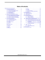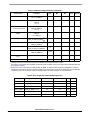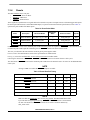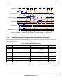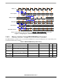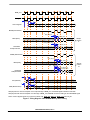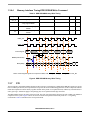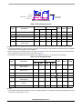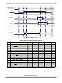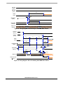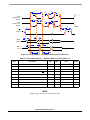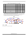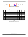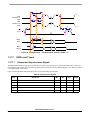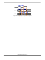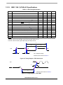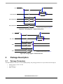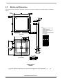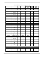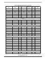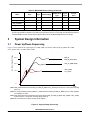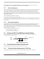
1
Freescale Semiconductor
Data Sheet: Technical Data
Document Number: MPC5200BDS
Rev. 4, 02/2010
MPC5200B Data Sheet
Key features are shown below.
• MPC603e series e300 core
– Superscalar architecture
– 760 MIPS at 400 MHz (–40 oC to +85 oC)
– 16 KB Instruction cache, 16 KB Data cache
– Double precision FPU
– Instruction and Data MMU
– Standard and Critical interrupt capability
• SDRAM / DDR Memory Interface
– Up to 133 MHz operation
– SDRAM and DDR SDRAM support
– 256 MB addressing range per CS, two CS available
– 32-bit data bus
– Built-in initialization and refresh
• Flexible multi-function External Bus Interface
– Supports interfacing to ROM/Flash/SRAM memories or
other memory mapped devices
– 8 programmable Chip Selects
– Non-multiplexed data access using 8-/16-/32-bit databus
with up to 26-bit address
– Short or Long Burst capable
– Multiplexed data access using 8-/16-/32-bit databus
with up to 25-bit address
• Peripheral Component Interconnect (PCI) Controller
– Version 2.2 PCI compatibility
– PCI initiator and target operation
– 32-bit PCI Address/Data bus
– 33 and 66 MHz operation
– PCI arbitration function
• ATA Controller
– Version 4 ATA compatible external interface—IDE Disk
Drive connectivity
• BestComm DMA subsystem
– Intelligent virtual DMA Controller
– Dedicated DMA channels to control peripheral
reception and transmission
– Local memory (SRAM 16 KB)
• 6 Programmable Serial Controllers (PSC)
– UART or RS232 interface
– CODEC interface for Soft Modem, Master/Slave
CODEC Mode, I2S and AC97
TEPBGA–272
27 mm x 27 mm
•
•
•
•
•
•
•
•
•
•
•
•
– Full duplex SPI mode
– IrDA mode from 2400 bps to 4 Mbps
Fast Ethernet Controller (FEC)
– Supports 100Mbps IEEE 802.3 MII, 10 Mbps IEEE
802.3 MII, 10 Mbps 7-wire interface
Universal Serial Bus Controller (USB)
– USB Revision 1.1 Host
– Open Host Controller Interface (OHCI)
– Integrated USB Hub, with two ports.
Two Inter-Integrated Circuit Interfaces (I2C)
Serial Peripheral Interface (SPI)
Dual CAN 2.0 A/B Controller (MSCAN)
– Implementation of version 2.0A/B CAN protocol
– Standard and extended data frames
J1850 Byte Data Link Controller (BDLC)
J1850 Class B data communication network interface
compatible and ISO compatible for low speed (<125 kbps)
serial data communications in automotive applications.
Supports 4X mode, 41.6 kbps
In-frame response (IFR) types 0, 1, 2, and 3 supported
Systems level features
– Interrupt Controller supports four external interrupt
request lines and 47 internal interrupt sources
– GPIO/Timer functions
Up to 56 total GPIO pins that support a variety of
interrupt/WakeUp capabilities.
Eight GPIO pins with timer capability supporting input
capture, output compare, and pulse width modulation
(PWM) functions
– Real-time Clock with one-second resolution
– Systems Protection (watch dog timer, bus monitor)
– Individual control of functional block clock sources
– Power management: Nap, Doze, Sleep, Deep Sleep
modes
– Support of WakeUp from low power modes by different
sources (GPIO, RTC, CAN)
Test/Debug features
– JTAG (IEEE 1149.1 test access port)
– Common On-chip Processor (COP) debug port
On-board PLL and clock generation
Freescale reserves the right to change the detail specifications as may be required to permit
improvements in the design of its products.
© Freescale Semiconductor, Inc., 2008, 2010. All rights reserved.
Table of Contents
1
Electrical and Thermal Characteristics . . . . . . . . . . . . . . . . . . .4
1.1 DC Electrical Characteristics . . . . . . . . . . . . . . . . . . . . .4
1.1.1 Absolute Maximum Ratings . . . . . . . . . . . . . . . . .4
1.1.2 Recommended Operating Conditions . . . . . . . . .4
1.1.3 DC Electrical Specifications. . . . . . . . . . . . . . . . .5
1.1.4 Electrostatic Discharge . . . . . . . . . . . . . . . . . . . .7
1.1.5 Power Dissipation . . . . . . . . . . . . . . . . . . . . . . . .7
1.1.6 Thermal Characteristics. . . . . . . . . . . . . . . . . . . .9
1.2 Oscillator and PLL Electrical Characteristics . . . . . . . .10
1.2.1 System Oscillator Electrical Characteristics . . .11
1.2.2 RTC Oscillator Electrical Characteristics . . . . . .11
1.2.3 System PLL Electrical Characteristics. . . . . . . .11
1.2.4 e300 Core PLL Electrical Characteristics . . . . .11
1.3 AC Electrical Characteristics. . . . . . . . . . . . . . . . . . . . .12
1.3.1 AC Test Timing Conditions: . . . . . . . . . . . . . . . .12
1.3.2 AC Operating Frequency Data. . . . . . . . . . . . . .13
1.3.3 Clock AC Specifications. . . . . . . . . . . . . . . . . . .13
1.3.4 Resets . . . . . . . . . . . . . . . . . . . . . . . . . . . . . . . .14
1.3.5 External Interrupts . . . . . . . . . . . . . . . . . . . . . . .15
1.3.6 SDRAM . . . . . . . . . . . . . . . . . . . . . . . . . . . . . . .17
1.3.7 PCI. . . . . . . . . . . . . . . . . . . . . . . . . . . . . . . . . . .21
1.3.8 Local Plus Bus . . . . . . . . . . . . . . . . . . . . . . . . . .23
1.3.9 ATA. . . . . . . . . . . . . . . . . . . . . . . . . . . . . . . . . . .28
1.3.10 Ethernet . . . . . . . . . . . . . . . . . . . . . . . . . . . . . . .38
1.3.11 USB . . . . . . . . . . . . . . . . . . . . . . . . . . . . . . . . . .40
1.3.12 SPI . . . . . . . . . . . . . . . . . . . . . . . . . . . . . . . . . . .41
1.3.13 MSCAN . . . . . . . . . . . . . . . . . . . . . . . . . . . . . . .45
2
3
4
5
1.3.14 I2C . . . . . . . . . . . . . . . . . . . . . . . . . . . . . . . . . . 45
1.3.15 J1850 . . . . . . . . . . . . . . . . . . . . . . . . . . . . . . . . 46
1.3.16 PSC . . . . . . . . . . . . . . . . . . . . . . . . . . . . . . . . . 47
1.3.17 GPIOs and Timers . . . . . . . . . . . . . . . . . . . . . . 54
1.3.18 IEEE 1149.1 (JTAG) AC Specifications . . . . . . 56
Package Description . . . . . . . . . . . . . . . . . . . . . . . . . . . . . . . 57
2.1 Package Parameters . . . . . . . . . . . . . . . . . . . . . . . . . . 57
2.2 Mechanical Dimensions. . . . . . . . . . . . . . . . . . . . . . . . 58
2.3 Pinout Listings . . . . . . . . . . . . . . . . . . . . . . . . . . . . . . . 59
System Design Information . . . . . . . . . . . . . . . . . . . . . . . . . . 64
3.1 Power Up/Down Sequencing . . . . . . . . . . . . . . . . . . . . 64
3.1.1 Power Up Sequence. . . . . . . . . . . . . . . . . . . . . 65
3.1.2 Power Down Sequence . . . . . . . . . . . . . . . . . . 65
3.2 System and CPU Core AVDD Power Supply Filtering. 65
3.3 Pull-up/Pull-down Resistor Requirements . . . . . . . . . . 65
3.3.1 Pull-down Resistor Requirements for TEST pins65
3.3.2 Pull-up Requirements for the PCI Control Lines 66
3.3.3 Pull-up/Pull-down Requirements for MEM_MDQS
Pins (SDRAM) . . . . . . . . . . . . . . . . . . . . . . . . . 66
3.3.4 .Pull-up/Pull-down Requirements for MEM_MDQS
Pins (DDR 16-bit Mode) . . . . . . . . . . . . . . . . . . 66
3.4 JTAG . . . . . . . . . . . . . . . . . . . . . . . . . . . . . . . . . . . . . . 66
3.4.1 JTAG_TRST . . . . . . . . . . . . . . . . . . . . . . . . . . . 66
3.4.2 e300 COP/BDM Interface . . . . . . . . . . . . . . . . 67
Ordering Information . . . . . . . . . . . . . . . . . . . . . . . . . . . . . . . 69
Document Revision History . . . . . . . . . . . . . . . . . . . . . . . . . . 70
MPC5200B Data Sheet, Rev. 4
2
Freescale Semiconductor
Freescale Semiconductor
Figure 1 shows a simplified MPC5200B block diagram.
SDRAM/DDR
Systems Interface Unit (SIU)
Real-Time Clock
SDRAM/DDR
Memory Controller
System Functions
603
e300 Core
Interrupt Controller
GPIO/Timers
MPC5200B Data Sheet, Rev. 4
Local Plus Controller
JTAG / COP
Interface
Local
Bus
SRAM
16 KB
Reset / Clock
Generation
BestComm
DMA
PCI Bus Controller
ATA Host Controller
CommBus
PSC
6x
Ethernet
I2C
2x
SPI
USB
2x
Figure 1. Simplified Block Diagram—MPC5200B
J1850
MSCAN
2x
3
1
Electrical and Thermal Characteristics
1.1
DC Electrical Characteristics
1.1.1
Absolute Maximum Ratings
The tables in this section describe the MPC5200B DC Electrical characteristics. Table 1 gives the absolute maximum ratings.
Table 1. Absolute Maximum Ratings(1)
Characteristic
Sym
Min
Max
Unit
SpecID
Supply voltage — e300 core and peripheral logic
VDD_CORE
–0.3
1.8
V
D1.1
VDD_IO,
VDD_MEM_IO
–0.3
3.6
V
D1.2
SYS_PLL_AVDD
–0.3
2.1
V
D1.3
CORE_PLL_AVDD
–0.3
2.1
V
D1.4
Input voltage (VDD_IO)
Vin
–0.3
VDD_IO + 0.3
V
D1.5
Input voltage (VDD_MEM_IO)
Vin
–0.3
VDD_MEM_IO
+ 0.3
V
D1.6
Input voltage overshoot
Vinos
—
1.0
V
D1.7
Input voltage undershoot
Vinus
—
1.0
V
D1.8
Storage temperature range
Tstg
–55
150
oC
D1.9
Supply voltage — I/O buffers
Supply voltage — System APLL
Supply voltage — e300 APLL
1
Absolute maximum ratings are stress ratings only, and functional operation at the maximums is not guaranteed.
Stresses beyond those listed may affect device reliability or cause permanent damage.
1.1.2
Recommended Operating Conditions
Table 2 gives the recommended operating conditions.
Table 2. Recommended Operating Conditions
Sym
Min(1)
Max(1)
Unit
SpecID
VDD_CORE
1.42
1.58
V
D2.1
VDD_IO
3.0
3.6
V
D2.2
Supply voltage — memory I/O buffers (SDR)
VDD_MEM_IOSDR
3.0
3.6
V
D2.3
Supply voltage — memory I/O buffers (DDR)
VDD_MEM_IODDR
2.42
2.63
V
D2.4
SYS_PLL_AVDD
1.42
1.58
V
D2.5
CORE_PLL_AVDD
1.42
1.58
V
D2.6
Characteristic
Supply voltage — e300 core and peripheral
logic
Supply voltage — standard I/O buffers
Supply voltage — System APLL
Supply voltage — e300 APLL
MPC5200B Data Sheet, Rev. 4
4
Freescale Semiconductor
Table 2. Recommended Operating Conditions (continued)
Sym
Min(1)
Max(1)
Unit
SpecID
Vin
0
VDD_IO
V
D2.7
Input voltage — memory I/O buffers (SDR)
VinSDR
0
VDD_MEM_IOSDR
V
D2.8
Input voltage — memory I/O buffers (DDR)
VinDDR
0
VDD_MEM_IODDR
V
D2.9
TA
–40
+85
o
C
D2.10
+115
o
C
D2.12
Characteristic
Input voltage — standard I/O buffers
Ambient operating temperature range(2)
Die junction operating temperature range
Tj
–40
1
These are recommended and tested operating conditions. Proper device operation outside these conditions is not
guaranteed.
2
Maximum e300 core operating frequency is 400 MHz.
1.1.3
DC Electrical Specifications
Table 3 gives the DC Electrical characteristics for the MPC5200B at recommended operating conditions (see Table 2).
Table 3. DC Electrical Specifications
Characteristic
Condition
Sym
Min
Max
Unit
SpecID
Input high voltage
Input type = TTL
VDD_IO/VDD_MEM_IOSDR
VIH
2.0
—
V
D3.1
Input high voltage
Input type = TTL
VDD_MEM_IODDR
VIH
1.7
—
V
D3.2
Input high voltage
Input type = PCI
VDD_IO
VIH
2.0
—
V
D3.3
Input high voltage
Input type = SCHMITT
VDD_IO
VIH
2.0
—
V
D3.4
Input high voltage
SYS_XTAL_IN
CVIH
2.0
—
V
D3.5
Input high voltage
RTC_XTAL_IN
CVIH
2.0
—
V
D3.6
Input low voltage
Input type = TTL
VDD_IO/VDD_MEM_IOSDR
VIL
—
0.8
V
D3.7
Input low voltage
Input type = TTL
VDD_MEM_IODDR
VIL
—
0.7
V
D3.8
Input low voltage
Input type = PCI
VDD_IO
VIL
—
0.8
V
D3.9
Input low voltage
Input type = SCHMITT
VDD_IO
VIL
—
0.8
V
D3.10
Input low voltage
SYS_XTAL_IN
CVIL
—
0.8
V
D3.11
Input low voltage
RTC_XTAL_IN
CVIL
—
0.8
V
D3.12
Input leakage current
Vin = 0 or
VDD_IO/VDD_IO_MEMSDR
IIN
—
±2
μA
D3.13
IIN
—
±10
μA
D3.14
(depending on input type
Input leakage current
(1)
SYS_XTAL_IN
Vin = 0 or VDD_IO
)
MPC5200B Data Sheet, Rev. 4
Freescale Semiconductor
5
Table 3. DC Electrical Specifications (continued)
Characteristic
Condition
Sym
Min
Max
Unit
SpecID
Input leakage current
RTC_XTAL_IN
Vin = 0 or VDD_IO
IIN
—
±10
μA
D3.15
Input current, pullup resistor
PULLUP
VDD_IO
Vin = 0
IINpu
40
109
μA
D3.16
Input current, pullup resistor
— memory I/O buffers
PULLUP_MEM
VDD_IO_MEMSDR
Vin = 0
IINpu
41
111
μA
D3.17
Input current, pulldown
resistor
PULLDOWN
VDD_IO
Vin = VDD_IO
IINpd
36
106
μA
D3.18
Output high voltage
IOH is driver dependent(2)
VDD_IO, VDD_IO_MEMSDR
VOH
2.4
—
V
D3.19
Output high voltage
IOH is driver dependent(2)
VDD_IO_MEMDDR
VOHDDR
1.7
—
V
D3.20
Output low voltage
IOL is driver dependent(2)
VDD_IO, VDD_IO_MEMSDR
VOL
—
0.4
V
D3.21
Output low voltage
IOL is driver dependent(2)
VDD_IO_MEMDDR
VOLDDR
—
0.4
V
D3.22
ICS
–1.0
1.0
mA
D3.23
Cin
—
15
pF
D3.24
DC Injection Current Per
Pin(3)
Capacitance
Vin = 0 V, f = 1 MHz
1
Leakage current is measured with output drivers disabled and pull-up/pull-downs inactive.
See Table 4 for the typical drive capability of a specific signal pin based on the type of output driver associated with that
pin as listed in Table 52.
3 All injection current is transferred to VDD_IO/VDD_IO_MEM. An external load is required to dissipate this current to
maintain the power supply within the specified voltage range. Total injection current for all digital input-only and all digital
input/output pins must not exceed 10 mA. Exceeding this limit can cause disruption of normal operation.
2
Table 4. Drive Capability of MPC5200B Output Pins
Driver Type
Supply Voltage
IOH
IOL
Unit
SpecID
DRV4
VDD_IO = 3.3 V
4
4
mA
D3.25
DRV8
VDD_IO = 3.3 V
8
8
mA
D3.26
DRV8_OD
VDD_IO = 3.3 V
—
8
mA
D3.27
DRV16_MEM
VDD_IO_MEM = 3.3 V
16
16
mA
D3.28
DRV16_MEM
VDD_IO_MEM = 2.5 V
16
16
mA
D3.29
PCI
VDD_IO = 3.3 V
16
16
mA
D3.30
MPC5200B Data Sheet, Rev. 4
6
Freescale Semiconductor
1.1.4
Electrostatic Discharge
CAUTION
This device contains circuitry that protects against damage due to high-static voltage or
electrical fields. However, it is advised that normal precautions be taken to avoid
application of any voltages higher than maximum-rated voltages. Operational
reliability is enhanced if unused inputs are tied to an appropriate logic voltage level (GND
or VCC ). Table 7 gives package thermal characteristics for this device.
Table 5. ESD and Latch-Up Protection Characteristics
Sym
Rating
Min
Max
Unit
SpecID
VHBM
Human Body Model (HBM)—JEDEC JESD22-A114-B
2000
—
V
D4.1
VMM
Machine Model (MM)—JEDEC JESD22-A115
200
—
V
D4.2
VCDM
Charge Device Model (CDM)—JEDEC JESD22-C101
500
—
V
D4.3
Latch-up Current at TA=85 oC
positive
negative
+100
–100
—
mA
Latch-up Current at TA=27 oC
positive
negative
+200
–200
—
mA
ILAT
ILAT
1.1.5
D4.4
D4.5
Power Dissipation
Power dissipation of the MPC5200B is caused by 3 different components: the dissipation of the internal or core digital logic
(supplied by VDD_CORE), the dissipation of the analog circuitry (supplied by SYS_PLL_AVDD and CORE_PLL_AVDD)
and the dissipation of the IO logic (supplied by VDD_IO_MEM and VDD_IO). Table 6 details typical measured core and
analog power dissipation figures for a range of operating modes. However, the dissipation due to the switching of the IO pins
can not be given in general, but must be calculated by the user for each application case using the following formula:
P IO = P IOint +
∑ N × C × VDD_IO
2
×f
Eqn. 1
M
where N is the number of output pins switching in a group M, C is the capacitance per pin, VDD_IO is the IO voltage swing, f
is the switching frequency and PIOint is the power consumed by the unloaded IO stage. The total power consumption of the
MPC5200B processor must not exceed the value, which would cause the maximum junction temperature to be exceeded.
P total = P core + P analog + P IO
Eqn. 2
MPC5200B Data Sheet, Rev. 4
Freescale Semiconductor
7
Table 6. Power Dissipation
Core Power Supply (VDD_CORE)
SYS_XTAL/XLB/PCI/IPB/CORE (MHz)
SpecID
Mode
33/66/33/33/264
33/132/66/132/396
Typ
Typ
Operational
727.5
Doze
Nap
Sleep
Deep-Sleep
Unit
Notes
1080
mW
(1),(2)
D5.1
—
600
mW
(1),(3)
D5.2
—
225
mW
(1),(4)
D5.3
mW
(1),(5)
D5.4
mW
(1),(6)
D5.5
—
225
52.5
52.5
PLL Power Supplies (SYS_PLL_AVDD, CORE_PLL_AVDD)
Mode
Typ
Unit
Notes
Typical
2
mW
(7)
D5.6
Unloaded I/O Power Supplies (VDD_IO, VDD_MEM_IO8)
1
2
3
4
5
6
7
8
9
Mode
Typ
Unit
Notes
Typical
33
mW
(9)
D5.7
Typical core power is measured at VDD_CORE = 1.5 V, Tj = 25 °C
Operational power is measured while running an entirely cache-resident program with floating-point multiplication
instructions in parallel with a continuous PCI transaction via BestComm.
Doze power is measured with the e300 core in Doze mode, the system oscillator, System PLL and Core PLL are
active, all other system modules are inactive
Nap power is measured with the e300 core in Nap mode, the system oscillator, System PLL and Core PLL are
active, all other system modules are inactive
Sleep power is measured with the e300 core in Sleep mode, the system oscillator, System PLL and Core PLL are
active, all other system modules are inactive
Deep-Sleep power is measured with the e300 core in Sleep mode, the system oscillator, System PLL, Core
PLL and all other system modules are inactive
Typical PLL power is measured at SYS_PLL_AVDD = CORE_PLL_AVDD = 1.5 V, Tj = 25 °C
IO power figures given in the table represent the worst case scenario. For the VDD_MEM_IO rail connected to
2.5 V the IO power is expected to be lower and bounded by the worst case with VDD_MEM_IO connected to 3.3 V.
Unloaded typical I/O power is measured in Deep-Sleep mode at VDD_IO = VDD_MEM_IOSDR= 3.3 V, Tj = 25 °C
MPC5200B Data Sheet, Rev. 4
8
Freescale Semiconductor
1.1.6
Thermal Characteristics
Table 7. Thermal Resistance Data
Rating
Board Layers
Sym
Value
Unit
Notes
SpecID
RθJA
30
°C/W
(1),(2)
D6.1
Junction to Ambient
Natural Convection
Single layer board
(1s)
Junction to Ambient
Natural Convection
Four layer board (2s2p)
RθJMA
22
°C/W
(1),(3)
D6.2
Junction to Ambient (@200
ft/min)
Single layer board
(1s)
RθJMA
24
°C/W
(1),(3)
D6.3
Junction to Ambient (@200
ft/min)
Four layer board
(2s2p)
RθJMA
19
°C/W
(1),(3)
D6.4
RθJB
14
°C/W
(4)
D6.5
D6.6
D6.7
Junction to Board
—
Junction to Case
Junction to Package Top
1
2
3
4
5
6
—
Natural Convection
RθJC
8
°C/W
(5)
ΨJT
2
°C/W
(6)
Junction temperature is a function of die size, on-chip power dissipation, package thermal resistance, mounting site
(board) temperature, ambient temperature, air flow, power dissipation of other components on the board, and board
thermal resistance.
Per SEMI G38-87 and JEDEC JESD51-2 with the single layer board horizontal.
Per JEDEC JESD51-6 with the board horizontal.
Thermal resistance between the die and the printed circuit board per JEDEC JESD51-8. Board temperature is
measured on the top surface of the board near the package.
Thermal resistance between the die and the case top surface as measured by the cold plate method (MIL
SPEC-883 Method 1012.1).
Thermal characterization parameter indicating the temperature difference between package top and the junction
temperature per JEDEC JESD51-2. When Greek letters are not available, the thermal characterization parameter
is written as Psi-JT.
1.1.6.1
Heat Dissipation
An estimation of the chip-junction temperature, TJ, can be obtained from the following equation:
TJ = TA +(R θJA × PD )
Eqn. 3
where:
TA = ambient temperature for the package (ºC)
R θJA = junction to ambient thermal resistance (ºC/W)
PD = power dissipation in package (W)
The junction to ambient thermal resistance is an industry standard value, which provides a quick and easy estimation of thermal
performance. Unfortunately, there are two values in common usage: the value determined on a single layer board, and the value
obtained on a board with two planes. For packages such as the PBGA, these values can be different by a factor of two. Which
value is correct depends on the power dissipated by other components on the board. The value obtained on a single layer board
is appropriate for the tightly packed printed circuit board. The value obtained on the board with the internal planes is usually
appropriate if the board has low power dissipation and the components are well separated.
Historically, the thermal resistance has frequently been expressed as the sum of a junction to case thermal resistance and a case
to ambient thermal resistance:
MPC5200B Data Sheet, Rev. 4
Freescale Semiconductor
9
R θJA = R θJC +R θCA
Eqn. 4
where:
R θJA = junction to ambient thermal resistance (ºC/W)
R θJC = junction to case thermal resistance (ºC/W)
R θCA = case to ambient thermal resistance (ºC/W)
R θJC is device related and cannot be influenced by the user. The user controls the thermal environment to change the case to
ambient thermal resistance, R θCA. For instance, the user can change the air flow around the device, add a heat sink, change the
mounting arrangement on printed circuit board, or change the thermal dissipation on the printed circuit board surrounding the
device. This description is most useful for ceramic packages with heat sinks where some 90% of the heat flow is through the
case to the heat sink to ambient. For most packages, a better model is required.
A more accurate thermal model can be constructed from the junction to board thermal resistance and the junction to case thermal
resistance. The junction to case covers the situation where a heat sink is used or a substantial amount of heat is dissipated from
the top of the package. The junction to board thermal resistance describes the thermal performance when most of the heat is
conducted to the printed circuit board. This model can be used for hand estimations or for a computational fluid dynamics (CFD)
thermal model.
To determine the junction temperature of the device in the application after prototypes are available, the Thermal
Characterization Parameter (ΨJT) can be used to determine the junction temperature with a measurement of the temperature at
the top center of the package case using the following equation:
TJ = TT +( Ψ JT × PD )
Eqn. 5
where:
TT = thermocouple temperature on top of package (ºC)
Ψ JT = thermal characterization parameter (ºC/W)
PD = power dissipation in package (W)
The thermal characterization parameter is measured per JESD51-2 specification using a 40-gauge type T thermocouple epoxied
to the top center of the package case. The thermocouple should be positioned, so that the thermocouple junction rests on the
package. A small amount of epoxy is placed over the thermocouple junction and over approximately one mm of wire extending
from the junction. The thermocouple wire is placed flat against the package case to avoid measurement errors caused by cooling
effects of the thermocouple wire.
1.2
Oscillator and PLL Electrical Characteristics
The MPC5200B System requires a system-level clock input SYS_XTAL. This clock input may be driven directly from an
external oscillator or with a crystal using the internal oscillator.
There is a separate oscillator for the independent Real-Time Clock (RTC) system.
The MPC5200B clock generation uses two phase locked loop (PLL) blocks.
•
•
The system PLL (SYS_PLL) takes an external reference frequency and generates the internal system clock. The
system clock frequency is determined by the external reference frequency and the settings of the SYS_PLL
configuration.
The e300 core PLL (CORE_PLL) generates a master clock for all of the CPU circuitry. The e300 core clock frequency
is determined by the system clock frequency and the settings of the CORE_PLL configuration.
MPC5200B Data Sheet, Rev. 4
10
Freescale Semiconductor
1.2.1
System Oscillator Electrical Characteristics
Table 8. System Oscillator Electrical Characteristics
1.2.2
Characteristic
Sym
SYS_XTAL frequency
Oscillator start-up time
Notes
Min
Typical
Max
Unit
SpecID
fsys_xtal
15.6
33.3
35.0
MHz
O1.1
tup_osc
—
—
10
ms
O1.2
RTC Oscillator Electrical Characteristics
Table 9. RTC Oscillator Electrical Characteristics
1.2.3
Characteristic
Sym
RTC_XTAL frequency
frtc_xtal
Notes
Min
Typical
Max
Unit
SpecID
—
32.768
—
kHz
O2.1
System PLL Electrical Characteristics
Table 10. System PLL Specifications
Characteristic
Sym
Notes
Min
Typical
Max
Unit
SpecID
SYS_XTAL frequency
fsys_xtal
(1)
15.6
33.3
35.0
MHz
O3.1
tsys_xtal
(1)
66.6
30.0
28.5
ns
O3.2
SYS_XTAL clock input jitter
tjitter
(2)
—
—
150
ps
O3.3
System VCO frequency
fVCOsys
(1)
250
533
800
MHz
O3.4
System PLL relock time
tlock
(3)
—
—
100
μs
O3.5
SYS_XTAL cycle time
1
The SYS_XTAL frequency and PLL Configuration bits must be chosen such that the resulting system frequency, CPU
(core) frequency, and PLL (VCO) frequency do not exceed their respective maximum or minimum operating
frequencies.
2 This represents total input jitter—short term and long term combined—and is guaranteed by design. Two different
types of jitter can exist on the input to CORE_SYSCLK, systemic and true random jitter. True random jitter is rejected.
Systemic jitter is passed into and through the PLL to the internal clock circuitry.
3 Relock time is guaranteed by design and characterization. PLL-relock time is the maximum amount of time required
for the PLL lock after a stable VDD and CORE_SYSCLKare reached during the power-on reset sequence. This
specification also applies when the PLL has been disabled and subsequently re-enabled during sleep modes.
1.2.4
e300 Core PLL Electrical Characteristics
The internal clocking of the e300 core is generated from and synchronized to the system clock by means of a voltage-controlled
core PLL.
MPC5200B Data Sheet, Rev. 4
Freescale Semiconductor
11
Table 11. e300 PLL Specifications
Characteristic
Sym
Notes
Min
Typical
Max
Unit
SpecID
e300 frequency
fcore
(1)
50
—
550
MHz
O4.1
e300 cycle time
tcore
(1)
2.85
—
40.0
ns
O4.2
e300 VCO frequency
fVCOcore
(1)
400
—
1200
MHz
O4.3
e300 input clock frequency
fXLB_CLK
—
25
—
367
MHz
O4.4
e300 input clock cycle time
tXLB_CLK
—
2.73
—
50.0
ns
O4.5
e300 input clock jitter
tjitter
(2)
—
—
150
ps
O4.6
tlock
(3)
—
—
100
μs
O4.7
e300 PLL relock time
1
The XLB_CLK frequency and e300 PLL Configuration bits must be chosen such that the resulting system
frequencies, CPU (core) frequency, and e300 PLL (VCO) frequency do not exceed their respective maximum or
minimum operating frequencies in Table 12.
2
This represents total input jitter—short term and long term combined—and is guaranteed by design. Two different
types of jitter can exist on the input to CORE_SYSCLK, systemic and true random jitter. True random jitter is rejected.
Systemic jitter is passed into and through the PLL to the internal clock circuitry.
3 Relock time is guaranteed by design and characterization. PLL-relock time is the maximum amount of time required
for the PLL lock after a stable VDD and CORE_SYSCLK are reached during the power-on reset sequence. This
specification also applies when the PLL has been disabled and subsequently re-enabled during sleep modes.
1.3
AC Electrical Characteristics
Hyperlinks to the indicated timing specification sections are provided below.
1.3.1
•
AC Operating Frequency Data
•
USB
•
Clock AC Specifications
•
SPI
•
Resets
•
MSCAN
•
External Interrupts
•
I2C
•
SDRAM
•
J1850
•
PCI
•
PSC
•
Local Plus Bus
•
GPIOs and Timers
•
ATA
•
IEEE 1149.1 (JTAG) AC Specifications
•
Ethernet
AC Test Timing Conditions:
Unless otherwise noted, all test conditions are as follows:
•
•
•
TA = –40 to 85 oC
Tj = –40 to 115 oC
VDD_CORE = 1.42 to 1.58 V
VDD_IO = 3.0 to 3.6 V
MPC5200B Data Sheet, Rev. 4
12
Freescale Semiconductor
•
•
Input conditions:
All Inputs: tr, tf <= 1 ns
Output Loading:
All Outputs: 50 pF
1.3.2
AC Operating Frequency Data
Table 12 provides the operating frequency information for the MPC5200B.
Table 12. Clock Frequencies
Min
Max
Units
SpecID
1
e300 Processor Core
—
400
MHz
A1.1
2
SDRAM Clock
—
133
MHz
A1.2
3
XL Bus Clock
—
133
MHz
A1.3
4
IP Bus Clock
—
133
MHz
A1.4
5
PCI / Local Plus Bus Clock
—
66
MHz
A1.5
6
PLL Input Range
15.6
35
MHz
A1.6
1.3.3
Clock AC Specifications
t CYCLE
t DUTY
t DUTY
t FALL
t RISE
CV IH
SYSCLK
VM
VM
VM
CV IL
Figure 2. Timing Diagram—SYS_XTAL_IN
Table 13. SYS_XTAL_IN Timing
Sym
t CYCLE
Description
(1)
SYS_XTAL_IN cycle time.
t RISE
SYS_XTAL_IN rise time.
t FALL
SYS_XTAL_IN fall time.
t DUTY
SYS_XTAL_IN duty cycle (measured at V M
).(2)
Min
Max
Units
SpecID
28.6
64.1
ns
A2.1
—
5.0
ns
A2.2
—
5.0
ns
A2.3
40.0
60.0
%
A2.4
CV IH
SYS_XTAL_IN input voltage high
2.0
—
V
A2.5
CV IL
SYS_XTAL_IN input voltage low
—
0.8
V
A2.6
1
CAUTION—The SYS_XTAL_IN frequency and system PLL_CFG[0–6] settings must be chosen such that the resulting
system frequencies do not exceed their respective maximum or minimum operating frequencies. See the MPC5200B
User’s Manual (MPC5200BUM).
2 SYS_XTAL_IN duty cycle is measured at V .
M
MPC5200B Data Sheet, Rev. 4
Freescale Semiconductor
13
1.3.4
Resets
The MPC5200B has three reset pins:
•
•
•
PORRESET—Power on Reset
HRESET—Hard Reset
SRESET—Software Reset
These signals are asynchronous I/O signals and can be asserted at any time. The input side uses a Schmitt trigger and requires
the same input characteristics as other MPC5200B inputs, as specified in the DC Electrical Specifications section. Table 14
specifies the pulse widths of the Reset inputs.
Table 14. Reset Pulse Width
Name
Description
Min Pulse Width
Max Pulse
Width
Reference Clock
SpecID
PORRESET
Power On Reset
tVDD_stable + tup_osc + tlock
—
SYS_XTAL_IN
A3.1
HRESET
Hardware Reset
4 clock cycles
—
SYS_XTAL_IN
A3.2
SRESET
Software Reset
4 clock cycles
—
SYS_XTAL_IN
A3.3
For PORRESET the value of the minimum pulse width reflects the power on sequence. If PORRESET is asserted afterwards
its minimum pulse width equals the minimum given for HRESET related to the same reference clock.
The tVDD_stable describes the time which is needed to get all power supplies stable.
For tlock, refer to the Oscillator/PLL section of this specification for further details.
For tup_osc, refer to the Oscillator/PLL section of this specification for further details.
Following the deassertion of PORRESET, HRESET and SRESET remain low for 4096 reference clock cycles.
The deassertion of HRESET for at least the minimum pulse width forces the internal resets to be active for an additional 4096
clock cycles.
NOTE
As long as VDD is not stable the HRESET output is not stable.
Table 15. Reset Rise/Fall Timing
Description
Min
Max
Unit
SpecID
PORRESET fall time
—
1
ms
A3.4
PORRESET rise time
—
1
ms
A3.5
HRESET fall time
—
1
ms
A3.6
HRESET rise time
—
1
ms
A3.7
SRESET fall time
—
1
ms
A3.8
SRESET rise time
—
1
ms
A3.9
NOTE
Make sure that the PORRESET does not carry any glitches. The MPC5200B has no filter
to prevent them from getting into the chip. HRESET and SRESET must have a monotonous
rise time. The assertion of HRESET becomes active at Power on Reset without any
SYS_XTAL clock.
MPC5200B Data Sheet, Rev. 4
14
Freescale Semiconductor
For additional information, see the MPC5200B User’s Manual (MPC5200BUM).
1.3.4.1
Reset Configuration Word
During reset (HRESET and PORRESET) the Reset Configuration Word is latched in the related Reset Configuration Word
Register with each rising edge of the SYS_XTAL signal. If both resets (HRESET and PORRESET) are inactive (high), the
contents of this register are locked immediately with the SYS_XTAL clock (see Figure 3).
4096 clocks
SYS_XTAL
PORRESET
HRESET
RST_CFG_WRD
sample sample sample sample
sample sample sample sample
sample
sample
LOCK
Figure 3. Reset Configuration Word Locking
NOTE
Beware of changing the values on the pins of the reset configuration word after the
deassertion of PORRESET. This may cause problems because it may change the internal
clock ratios and so extend the PLL locking process.
1.3.5
External Interrupts
The MPC5200B provides three different kinds of external interrupts:
•
•
•
Four IRQ interrupts
Eight GPIO interrupts with simple interrupt capability (not available in power-down mode)
Eight WakeUp interrupts (special GPIO pins)
The propagation of these three kinds of interrupts to the core is shown in the following graphic:
MPC5200B Data Sheet, Rev. 4
Freescale Semiconductor
15
IRQ0
cint
CORE_CINT
Encoder
8 GPIOs
8
CORE_INT
GPIO Std
int
8 GPIOs
8
GPIO WakeUp
e300 Core
Grouper
Encoder
IRQ1
IRQ2
PIs
Main Interrupt
Controller
IRQ3
Notes:
1. PIs = Programmable Inputs
2. Grouper and Encoder functions imply programmability in software
Figure 4. External Interrupt Scheme
Due to synchronization, prioritization, and mapping of external interrupt sources, the propagation of external interrupts to the
core processor is delayed by several IP_CLK clock cycles. The following table specifies the interrupt latencies in IP_CLK
cycles. The IP_CLK frequency is programmable in the Clock Distribution Module (see Table 16).
Table 16. External Interrupt Latencies
Interrupt Type
Pin Name
Clock Cycles
Reference Clock
Core Interrupt
SpecID
Interrupt Requests
IRQ0
10
IP_CLK
critical (cint)
A4.1
IRQ0
10
IP_CLK
normal (int)
A4.2
IRQ1
10
IP_CLK
normal (int)
A4.3
IRQ2
10
IP_CLK
normal (int)
A4.4
IRQ3
10
IP_CLK
normal (int)
A4.5
GPIO_PSC3_4
12
IP_CLK
normal (int)
A4.6
GPIO_PSC3_5
12
IP_CLK
normal (int)
A4.7
GPIO_PSC3_8
12
IP_CLK
normal (int)
A4.8
GPIO_USB_9
12
IP_CLK
normal (int)
A4.9
GPIO_ETHI_4
12
IP_CLK
normal (int)
A4.10
GPIO_ETHI_5
12
IP_CLK
normal (int)
A4.11
GPIO_ETHI_6
12
IP_CLK
normal (int)
A4.12
GPIO_ETHI_7
12
IP_CLK
normal (int)
A4.13
GPIO_PSC1_4
12
IP_CLK
normal (int)
A4.15
GPIO_PSC2_4
12
IP_CLK
normal (int)
A4.16
GPIO_PSC3_9
12
IP_CLK
normal (int)
A4.17
GPIO_ETHI_8
12
IP_CLK
normal (int)
A4.18
GPIO_IRDA_0
12
IP_CLK
normal (int)
A4.19
DGP_IN0
12
IP_CLK
normal (int)
A4.20
DGP_IN1
12
IP_CLK
normal (int)
A4.21
Standard GPIO Interrupts
GPIO WakeUp Interrupts
NOTES:
1) The frequency of IP_CLK depends on register settings in Clock Distribution Module. See the MPC5200B User’s Manual.
MPC5200B Data Sheet, Rev. 4
16
Freescale Semiconductor
2) The interrupt latency descriptions in the table above are related to non competitive, non masked but enabled external interrupt
sources. Take care of interrupt prioritization which may increase the latencies.
Because all external interrupt signals are synchronized into the internal processor bus clock domain, each of these signals has
to exceed a minimum pulse width of more than one IP_CLK cycle.
Table 17. Minimum Pulse Width for External Interrupts to be Recognized
Name
Min Pulse Width
Max Pulse Width
Reference Clock
SpecID
All external interrupts (IRQs, GPIOs)
> 1 clock cycle
—
IP_CLK
A4.22
NOTES:
1) The frequency of the IP_CLK depends on the register settings in Clock Distribution Module. See the MPC5200B User’s Manual
(MPC5200BUM) for further information.
2) If the same interrupt occurs a second time while its interrupt service routine has not cleared the former one, the second
interrupt is not recognized at all.
Besides synchronization, prioritization, and mapping the latency of an external interrupt to the start of its associated interrupt
service routine also depends on the following conditions: To get a minimum interrupt service response time, it is recommended
to enable the instruction cache and set up the maximum core clock, XL bus, and IP bus frequencies (depending on board design
and programming). In addition, it is advisable to execute an interrupt handler, which has been implemented in assembly code.
1.3.6
1.3.6.1
SDRAM
Memory Interface Timing-Standard SDRAM Read Command
Table 18. Standard SDRAM Memory Read Timing
Sym
Description
Min
Max
Units
SpecID
tmem_clk
MEM_CLK period
7.5
—
ns
A5.1
tvalid
Control Signals, Address and MBA Valid after
rising edge of MEM_CLK
—
tmem_clk × 0.5 + 0.4
ns
A5.2
thold
Control Signals, Address and MBA Hold after
rising edge of MEM_CLK
tmem_clk × 0.5
—
ns
A5.3
DMvalid
DQM valid after rising edge of MEM_CLK
—
tmem_clk × 0.25 + 0.4
ns
A5.4
DMhold
DQM hold after rising edge of MEM_CLK
tmem_clk × 0.25 – 0.7
—
ns
A5.5
datasetup
MDQ setup to rising edge of MEM_CLK
—
0.3
ns
A5.6
datahold
MDQ hold after rising edge of MEM_CLK
0.2
—
ns
A5.7
MPC5200B Data Sheet, Rev. 4
Freescale Semiconductor
17
MEM_CLK
tvalid
thold
Active
Control Signals
NOP
READ
DMvalid
NOP
NOP
NOP
NOP
NOP
DMhold
DQM (Data Mask)
datasetup
datahold
MDQ (Data)
tvalid
thold
Row
MA (Address)
Column
tvalid
thold
MBA (Bank Selects)
NOTE: Control Signals are composed of RAS, CAS, MEM_WE, MEM_CS, MEM_CS1 and CLK_EN
Figure 5. Timing Diagram—Standard SDRAM Memory Read Timing
1.3.6.2
Memory Interface Timing-Standard SDRAM Write Command
In Standard SDRAM, all signals are activated on the MEM_CLK from the Memory Controller and captured on the MEM_CLK
clock at the memory device.
Table 19. Standard SDRAM Write Timing
Sym
Description
Min
Max
Units
SpecID
tmem_clk
MEM_CLK period
7.5
—
ns
A5.8
tvalid
Control Signals, Address and MBA Valid
after rising edge of MEM_CLK
—
tmem_clk × 0.5 + 0.4
ns
A5.9
thold
Control Signals, Address and MBA Hold after
rising edge of MEM_CLK
tmem_clk × 0.5
—
ns
A5.10
DMvalid
DQM valid after rising edge of MEM_CLK
—
tmem_clk × 0.25 + 0.4
ns
A5.11
DMhold
DQM hold after rising edge of Mem_clk
tmem_clk × 0.25 – 0.7
—
ns
A5.12
datavalid
MDQ valid after rising edge of MEM_CLK
—
tmem_clk × 0.75 + 0.4
ns
A5.13
datahold
MDQ hold after rising edge of MEM_CLK
tmem_clk × 0.75 – 0.7
—
ns
A5.14
MPC5200B Data Sheet, Rev. 4
18
Freescale Semiconductor
MEM_CLK
tvalid
thold
Active
Control Signals
NOP
WRITE
NOP
NOP
NOP
NOP
NOP
DMhold
DMvalid
DQM (Data Mask)
datavalid
datahold
MDQ (Data)
tvalid
thold
Row
MA (Address)
tvalid
Column
thold
MBA (Bank Selects)
NOTE: Control Signals are composed of RAS, CAS, MEM_WE, MEM_CS, MEM_CS1 and CLK_EN
Figure 6. Timing Diagram—Standard SDRAM Memory Write Timing
1.3.6.3
Memory Interface Timing-DDR SDRAM Read Command
The SDRAM Memory Controller uses a 1/4 period delayed MDQS strobe to capture the MDQ data. The 1/4 period delay value
is calculated automatically by hardware.
Table 20. DDR SDRAM Memory Read Timing
Sym
Description
Min
Max
Units
SpecID
tmem_clk
MEM_CLK period
7.5
—
ns
A5.15
tvalid
Control Signals, Address and MBA
valid after rising edge of MEM_CLK
—
tmem_clk × 0.5 + 0.4
ns
A5.16
thold
Control Signals, Address and MBA
hold after rising edge of MEM_CLK
tmem_clk × 0.5
—
ns
A5.17
datasetup
Setup time relative to MDQS
—
0.4
ns
A5.18
datahold
Hold time relative to MDQS
2.6
—
ns
A5.19
MPC5200B Data Sheet, Rev. 4
Freescale Semiconductor
19
MEM_CLK
MEM_CLK
tvalid
thold
Active
Control Signals
NOP
READ
NOP
NOP
NOP
NOP
NOP
MDQS (Data Strobe)
tdata_valid_min
tdata_valid_max
MDQ (Data)
Sample
position
A
tdata_sample_min
tdata_sample_max
Read Data
Sample Window
MDQS (Data Strobe)
tdata_valid_min
tdata_valid_max
MDQ (Data)
0.5
× tMEM_CLK
tdata_sample_min
tdata_sample_max
Sample
position
B
Read Data
Sample Window
tvalid
MA (Address)
thold
Row
tvalid
Column
thold
MBA (Bank Selects)
Sample position A: data are sampled on the expected edge of MEM_CLK, the MDQS signal indicate the valid data
Sample position B: data are sampled on a later edge of MEM_CLK, SDRAM controller is waiting for the valid MDQS signal
NOTE: Control Signals signals are composed of RAS, CAS, MEM_WE, MEM_CS, MEM_CS1 and CLK_EN
Figure 7. Timing Diagram—DDR SDRAM Memory Read Timing
MPC5200B Data Sheet, Rev. 4
20
Freescale Semiconductor
1.3.6.4
Memory Interface Timing-DDR SDRAM Write Command
Table 21. DDR SDRAM Memory Write Timing
Sym
Description
Min
Max
Units
SpecID
tmem_clk
MEM_CLK period
7.5
—
ns
A5.20
tDQSS
Delay from write command to first
rising edge of MDQS
—
tmem_clk + 0.4
ns
A5.21
datavalid
MDQ valid before rising edge of
MDQS
1.0
—
ns
A5.22
datahold
MDQ valid after rising edge of
MDQS
1.0
—
ns
A5.23
MEM_CLK
MEM_CLK
Control Signals
Write
Write
Write
Write
datavalid
datahold
MDQS (Data Strobe)
tDQSS
MDQ (Data)
NOTE: Control Signals signals are composed of RAS, CAS, MEM_WE, MEM_CS, MEM_CS1, and CLK_EN
Figure 8. DDR SDRAM Memory Write Timing
1.3.7
PCI
The PCI interface on the MPC5200B is designed to PCI Version 2.2 and supports 33 MHz and 66 MHz PCI operations. See the
PCI Local Bus Specification; the component section specifies the electrical and timing parameters for PCI components with the
intent that components connect directly together whether on the planar or an expansion board, without any external buffers or
other “glue logic.” Parameters apply at the package pins, not at expansion board edge connectors.
The MPC5200B is always the source of the PCI CLK. The clock waveform must be delivered to each 33 MHz or 66 MHz PCI
component in the system. Figure 9 shows the clock waveform and required measurement points for 3.3 V signaling
environments. Table 22 summarizes the clock specifications.
MPC5200B Data Sheet, Rev. 4
Freescale Semiconductor
21
t cyc
t high
t low
0.6 Vcc
0.5 Vcc
0.4 Vcc
PCI CLK
0.3 Vcc
0.4 Vcc, p-to-p
(minimum)
0.2 Vcc
Figure 9. PCI CLK Waveform
Table 22. PCI CLK Specifications
66 MHz
Sym
33 MHz
Description
Min
Max
Min
Max
Units
Notes
SpecID
tcyc
PCI CLK Cycle Time
15
30
30
—
ns
(1),(3)
A6.1
thigh
PCI CLK High Time
6
—
11
—
ns
—
A6.2
t low
PCI CLK Low Time
6
—
11
—
ns
—
A6.3
—
PCI CLK Slew Rate
1.5
4
1
4
V/ns
(2)
A6.4
—
PCI Clock Jitter
(peak to peak)
—
200
—
200
ps
—
—
NOTES:
1. In general, all 66 MHz PCI components must work with any clock frequency up to 66 MHz. CLK requirements vary depending
upon whether the clock frequency is above 33 MHz.
2. Rise and fall times are specified in terms of the edge rate measured in V/ns. This slew rate must be met across the minimum
peak-to-peak portion of the clock waveform as shown in Figure 9.
3. The minimum clock period must not be violated for any single clock cycle, i.e., accounting for all system jitter.
Table 23. PCI Timing Parameters
66 MHz
Sym
33 MHz
Description
Min
Max
Min
Max
Units
Notes
SpecID
tval
CLK to Signal Valid Delay —
bused signals
2
6
2
11
ns
(1),(2),(3)
A6.5
tval(ptp)
CLK to Signal Valid Delay —
point to point
2
6
2
12
ns
(1),(2),(3)
A6.6
t on
Float to Active Delay
2
—
2
—
ns
(1)
A6.7
28
ns
(1)
A6.8
t off
Active to Float Delay
t su
Input Setup Time to CLK —
bused signals
t su(ptp) Input Setup Time to CLK — point
to point
th
Input Hold Time from CLK
14
3
—
7
—
ns
(3),(4)
A6.9
5
—
10,12
—
ns
(3),(4)
A6.10
0
—
0
—
ns
(4)
A6.11
NOTES:
1. See the timing measurement conditions in the PCI Local Bus Specification. It is important that all driven signal transitions drive
to their Voh or Vol level within one Tcyc.
MPC5200B Data Sheet, Rev. 4
22
Freescale Semiconductor
2. Minimum times are measured at the package pin with the load circuit, and maximum times are measured with the load circuit
as shown in the PCI Local Bus Specification.
3. REQ# and GNT# are point-to-point signals and have different input setup times than do bused signals. GNT# and REQ# have
a setup of 5 ns at 66 MHz. All other signals are bused.
4. See the timing measurement conditions in the PCI Local Bus Specification.
For Measurement and Test Conditions, see the PCI Local Bus Specification.
1.3.8
Local Plus Bus
The Local Plus Bus is the external bus interface of the MPC5200B. A maximum of eight configurable chip selects (CS) are
provided. There are two main modes of operation: non-MUXed (Legacy and Burst) and MUXED. The reference clock is the
PCI CLK. The maximum bus frequency is 66 MHz.
Definition of Acronyms and Terms:
•
•
•
•
•
•
WS = Wait State
DC = Dead Cycle
LB = Long Burst
DS = Data Size in Bytes
tPCIck = PCI clock period
tIPBIck = IPBI clock period
tPCIck
PCI CLK
tIPBIck
IPBI CLK
Figure 10. Timing Diagram—IPBI and PCI clock (example ratio: 4:1)
1.3.8.1
Non-MUXed Mode
Table 24. Non-MUXed Mode Timing
Sym
Description
Min
Max
Units
Notes SpecID
t CSA
PCI CLK to CS assertion
4.6
10.6
ns
—
A7.1
t CSN
PCI CLK to CS negation
2.9
7.0
ns
—
A7.2
A7.3
t1
CS pulse width
(2 + WS) × tPCIck
(2 + WS) × tPCIck
ns
(1)
t2
ADDR valid before CS assertion
tIPBIck
tPCIck
ns
—
A7.4
t3
ADDR hold after CS negation
tIPBIck
—
ns
(2)
A7.5
t4
OE assertion before CS assertion
—
4.8
ns
—
A7.6
t5
OE negation before CS negation
—
2.7
ns
—
A7.7
t6
RW valid before CS assertion
tPCIck
—
ns
—
A7.8
t7
RW hold after CS negation
tIPBIck
—
ns
—
A7.9
t8
DATA output valid before CS assertion
tIPBIck
—
ns
—
A7.10
t9
DATA output hold after CS negation
tIPBIck
—
ns
—
A7.11
MPC5200B Data Sheet, Rev. 4
Freescale Semiconductor
23
Table 24. Non-MUXed Mode Timing (continued)
Sym
Description
Min
Max
Units
t10
DATA input setup before CS negation
8.5
—
ns
—
A7.12
ns
(6)
A7.13
A7.14
t11
DATA input hold after CS negation
0
(DC + 1) × tPCIck
Notes SpecID
t12
ACK assertion after CS assertion
tPCIck
—
ns
(3)
t13
ACK negation after CS negation
—
tPCIck
ns
(3)
A7.15
ns
(4)
A7.16
ns
(4)
A7.17
A7.18
t14
t15
TS assertion before CS assertion
TS pulse width
—
tPCIck
6.9
tPCIck
t16
TSIZ valid before CS assertion
tIPBIck
—
ns
(5)
t17
TSIZ hold after CS negation
tIPBIck
—
ns
(5)
A7.19
ns
(1)
A7.20
ns
(1)
A7.21
t18
t19
ACK change before PCI clock
ACK change after PCI clock
—
—
2.0
4.4
NOTES:
1. ACK can shorten the CS pulse width.
Wait States (WS) can be programmed in the Chip Select X Register, Bit field WaitP and WaitX. It can be specified from
0–65535.
2. In Large Flash and MOST Graphics mode the shared PCI/ATA pins, used as address lines, are released at the same moment
as the CS. This can cause the address to change before CS is deasserted.
3. ACK is input and can be used to shorten the CS pulse width.
4. Only available in Large Flash and MOST Graphics mode.
5. Only available in MOST Graphics mode.
6. Deadcycles are only used, if no arbitration to an other module (ATA or PCI) of the shared local bus happens. If arbitration
happens the bus can be driven within 4 IPB clocks by an other modules.
MPC5200B Data Sheet, Rev. 4
24
Freescale Semiconductor
PCI CLK
t1
CS[x]
t2
t3
ADDR
t5
t4
OE
t6
t7
R/W
t8
t9
DATA (wr)
t10
t11
DATA (rd)
t19
t12
ACK
t14
t13
t18
t15
TS
t17
TSIZ[1:2]
t16
Figure 11. Timing Diagram—Non-MUXed Mode
1.3.8.2
Burst Mode
Table 25. Burst Mode Timing
Sym
Description
Min
Max
t CSA
PCI CLK to CS assertion
4.6
10.6
ns
t CSN
PCI CLK to CS negation
2.9
7.0
4LB
4LB
Units Notes SpecID
—
A7.22
ns
—
A7.23
A7.24
t1
CS pulse width
(1 + WS +
×2
× (32/DS)) × tPCIck
(1 + WS +
×2×
(32/DS)) × tPCIck
ns
(1),(2)
t2
ADDR valid before CS assertion
tIPBIck
tPCIck
ns
—
A7.25
t3
ADDR hold after CS negation
–0.7
—
ns
—
A7.26
t4
OE assertion before CS assertion
—
4.8
ns
—
A7.27
t5
OE negation before CS negation
—
2.7
ns
—
A7.28
t6
RW valid before CS assertion
tPCIck
—
ns
—
A7.29
t7
RW hold after CS negation
tPCIck
—
ns
—
A7.30
t8
DATA setup before rising edge of
PCI clock
3.6
—
ns
—
A7.31
MPC5200B Data Sheet, Rev. 4
Freescale Semiconductor
25
Table 25. Burst Mode Timing (continued)
Sym
Description
Min
Max
Units Notes SpecID
t9
DATA hold after rising edge of PCI
clock
0
—
ns
—
A7.32
t10
DATA hold after CS negation
0
(DC + 1) × tPCIck
ns
(4)
A7.33
t11
ACK assertion after CS assertion
—
(WS + 1) × tPCIck
ns
—
A7.34
t12
ACK negation before CS negation
—
7.0
ns
(3)
A7.35
t13
ACK pulse width
ns
(2),(3)
A7.36
t14
CS assertion after TS assertion
—
2.5
ns
—
A7.37
t15
TS pulse width
tPCIck
tPCIck
ns
—
A7.38
4LB × 2 × (32/DS) × tPCIck 4LB × 2 × (32/DS) × tPCIck
NOTES:
1. Wait States (WS) can be programmed in the Chip Select X Register, Bit field WaitP and WaitX. It can be specified from
0–65535.
2. Example:
Long Burst is used, this means the CS related BERx and SLB bits of the Chip Select Burst Control Register are set and a burst
on the internal XLB is executed. => LB = 1
Data bus width is 8 bit. => DS = 8
=> 41 × 2 × (32/8) = 32 => ACK is asserted for 32 PCI cycles to transfer one cache line.
Wait State is set to 10. => WS = 10
1 + 10 + 32 = 43 => CS is asserted for 43 PCI cycles.
3. ACK is output and indicates the burst.
4. Deadcycles are only used, if no arbitration to an other module (ATA or PCI) of the shared local bus happens. If arbitration
happens the bus can be driven within 4 IPB clocks by an other modules.
PCI CLK
CS[x]
t1
t2
t3
ADDR
t5
t4
OE
t6
t7
R/W
t8
t10
DATA (rd)
t9
t11
t12
ACK
t14
t15
t13
TS
Figure 12. Timing Diagram—Burst Mode
MPC5200B Data Sheet, Rev. 4
26
Freescale Semiconductor
1.3.8.3
MUXed Mode
Table 26. MUXed Mode Timing
Sym
Description
Min
Max
Units
Notes
SpecID
t CSA
PCI CLK to CS assertion
4.6
10.6
ns
—
A7.39
t CSN
PCI CLK to CS negation
2.9
7.0
ns
—
A7.40
tALEA
PCI CLK to ALE assertion
—
3.6
ns
—
A7.41
t1
ALE assertion before Address, Bank,
TSIZ assertion
—
5.7
ns
—
A7.42
t2
CS assertion before Address, Bank,
TSIZ negation
—
–1.2
ns
—
A7.43
t3
CS assertion before Data wr valid
—
–1.2
ns
—
A7.44
t4
Data wr hold after CS negation
tIPBIck
—
ns
—
A7.45
t5
Data rd setup before CS negation
8.5
—
ns
—
A7.46
t6
Data rd hold after CS negation
0
(DC + 1) × tPCIck
ns
(1),(3)
A7.47
t7
ALE pulse width
—
tPCIck
ns
—
A7.48
tTSA
CS assertion after TS assertion
—
6.9
ns
—
A7.49
t8
TS pulse width
—
tPCIck
ns
—
A7.50
t9
CS pulse width
ns
—
A7.51
tOEA
OE assertion before CS assertion
—
4.7
ns
—
A7.52
tOEN
OE negation before CS negation
—
5.9
ns
—
A7.53
t10
RW assertion before ALE assertion
tIPBIck
—
ns
—
A7.54
t11
RW negation after CS negation
—
tPCIck
ns
—
A7.55
t12
ACK assertion after CS assertion
tIPBIck
—
ns
(2)
A7.56
(2)
A7.57
(2 + WS) × tPCIck (2 + WS) × tPCIck
t13
ACK negation after CS negation
—
tPCIck
ns
t14
ALE negation to CS assertion
—
tPCIck
ns
A7.58
t15
ACK change before PCI clock
—
2.0
ns
(2)
t16
ACK change after PCI clock
—
4.4
ns
(2)
A7.59
A7.60
NOTES:
1. ACK can shorten the CS pulse width.
Wait States (WS) can be programmed in the Chip Select X Register, Bit field WaitP and WaitX. It can be specified from
0–65535.
2. ACK is input and can be used to shorten the CS pulse width.
3. Deadcycles are only used, if no arbitration to an other module (ATA or PCI) of the shared local bus happens. If arbitration
happens the bus can be driven within 4 IPB clocks by an other modules.
MPC5200B Data Sheet, Rev. 4
Freescale Semiconductor
27
PCI CLK
t2
t1
t4
AD[31,27] (wr)
Data
AD[30:28] (wr)
TSIZ[0:2] bits
Data
AD[26:25] (wr)
Bank[0:1] bits
Data
AD[24:0] (wr)
Address[7:31]
Data
t3
t5
AD[31:0] (rd)
t6
Data
t7
t14
ALE
t8
Address latch
TS
t9
CSx
OE
t10
t11
R/W
t16
t12
ACK
t15
Address tenure
t13
Data tenure
Figure 13. Timing Diagram—MUXed Mode
1.3.9
ATA
The MPC5200B ATA Controller is completely software programmable. It can be programmed to operate with ATA protocols
using their respective timing, as described in the ANSI ATA-4 specification. The ATA interface is completely asynchronous in
nature. Signal relationships are based on specific fixed timing in terms of timing units (nanoseconds).
ATA data setup and hold times, with respect to Read/Write strobes, are software programmable inside the ATA Controller. Data
setup and hold times are implemented using counters. The counters count the number of ATA clock cycles needed to meet the
ANSI ATA-4 timing specifications. For details, see the ANSI ATA-4 specification and how to program an ATA Controller and
ATA drive for different ATA protocols and their respective timing. See the MPC5200B User’s Manual (MPC5200BUM).
The MPC5200B ATA Host Controller design makes data available coincidentally with the active edge of the WRITE strobe in
PIO and Multiword DMA modes.
•
•
Write data is latched by the drive at the inactive edge of the WRITE strobe. This gives ample setup time beyond that
required by the ATA-4 specification.
Data is held unchanged until the next active edge of the WRITE strobe. This gives ample hold time beyond that
required by the ATA-4 specification.
MPC5200B Data Sheet, Rev. 4
28
Freescale Semiconductor
All ATA transfers are programmed in terms of system clock cycles (IP bus clocks) in the ATA Host Controller timing registers.
This puts constraints on the ATA protocols and their respective timing modes in which the ATA Controller can communicate
with the drive.
Faster ATA modes (i.e., UDMA 0, 1, 2) are supported when the system is running at a sufficient frequency to provide adequate
data transfer rates. Adequate data transfer rates are a function of the following:
• The MPC5200B operating frequency (IP bus clock frequency)
• Internal MPC5200B bus latencies
• Other system load dependent variables
The ATA clock is the same frequency as the IP bus clock in MPC5200B. See the MPC5200B User’s Manual (MPC5200B).
NOTE
All output timing numbers are specified for nominal 50 pF loads.
Table 27. PIO Mode Timing Specifications
Sym
PIO Timing Parameter
Min/Max
(ns)
Mode 0
(ns)
Mode 1
(ns)
Mode 2
(ns)
Mode 3
(ns)
Mode 4
(ns)
SpecID
t0
Cycle Time
min
600
383
240
180
120
A8.1
t1
Address valid to DIOR/DIOW setup
min
70
50
30
30
25
A8.2
t2
DIOR/DIOW pulse width 16-bit
8-bit
min
min
165
290
125
290
100
290
80
80
70
70
A8.3
t2i
DIOR/DIOW recovery time
min
—
—
—
70
25
A8.4
t3
DIOW data setup
min
60
45
30
30
20
A8.5
t4
DIOW data hold
min
30
20
15
10
10
A8.6
t5
DIOR data setup
min
50
35
20
20
20
A8.7
t6
DIOR data hold
min
5
5
5
5
5
A8.8
t9
DIOR/DIOW to address
valid hold
min
20
15
10
10
10
A8.9
tA
IORDY setup
max
35
35
35
35
35
A8.10
tB
IORDY pulse width
max
1250
1250
1250
1250
1250
A8.11
MPC5200B Data Sheet, Rev. 4
Freescale Semiconductor
29
CS[0]/CS[3]/DA[2:0]
t2
DIOR/DIOW
t9
t1
t0
t3
t4
WDATA
t5
t6
RDATA
tA
tB
IORDY
Figure 14. PIO Mode Timing
Table 28. Multiword DMA Timing Specifications
Sym
Multiword DMA Timing Parameters
Min/Max
Mode 0(ns)
Mode 1(ns)
Mode 2(ns)
SpecID
t0
Cycle Time
min
480
150
120
A8.12
tC
DMACK to DMARQ delay
max
—
—
—
A8.13
tD
DIOR/DIOW pulse width (16-bit)
min
215
80
70
A8.14
tE
DIOR data access
max
150
60
50
A8.15
tG
DIOR/DIOW data setup
min
100
30
20
A8.16
tF
DIOR data hold
min
5
5
5
A8.17
tH
DIOW data hold
min
20
15
10
A8.18
tI
DMACK to DIOR/DIOW setup
min
0
0
0
A8.19
tJ
DIOR/DIOW to DMACK hold
min
20
5
5
A8.20
tKr
DIOR negated pulse width
min
50
50
25
A8.21
tKw
DIOW negated pulse width
min
215
50
25
A8.22
tLr
DIOR to DMARQ delay
max
120
40
35
A8.23
tLw
DIOW to DMARQ delay
max
40
40
35
A8.24
MPC5200B Data Sheet, Rev. 4
30
Freescale Semiconductor
t0
DMARQ
(Drive)
tL
tC
DMACK
(Host)
tD
tI
tJ
tK
DIOR
DIOW
(Host)
tE
RDATA
(Drive)
tF
WDATA
(Host)
tG
tH
Figure 15. Multiword DMA Timing
NOTE
The direction of signal assertion is towards the top of the page, and the direction of negation
is towards the bottom of the page, irrespective of the electrical properties of the signal.
Table 29. Ultra DMA Timing Specification
Sym
MODE 0
(ns)
MODE 1
(ns)
MODE 2
(ns)
Comment
SpecID
Min
Max
Min
Max
Min
Max
t CYC
114
—
75
—
55
—
Cycle time allowing for asymmetry and clock
variations from STROBE edge to STROBE edge
A8.26
t 2CYC
235
—
156
—
117
—
Two-cycle time allowing for clock variations, from
rising edge to next rising edge or from falling edge to
next falling edge of STROBE.
A8.27
t DS
15
—
10
—
7
—
Data setup time at recipient.
A8.28
t DH
5
—
5
—
5
—
Data hold time at recipient.
A8.29
t DVS
70
—
48
—
34
—
Data valid setup time at sender, to STROBE edge.
A8.30
t DVH
6
—
6
—
6
—
Data valid hold time at sender, from STROBE edge.
A8.31
t FS
0
230
0
200
0
170
First STROBE time for drive to first negate DSTROBE
from STOP during a data-in burst.
A8.32
t LI
0
150
0
150
0
150
Limited Interlock time.
A8.33
t MLI
20
—
20
—
20
—
Interlock time with minimum.
A8.34
t UI
0
—
0
—
0
—
Unlimited interlock time.
A8.35
MPC5200B Data Sheet, Rev. 4
Freescale Semiconductor
31
Table 29. Ultra DMA Timing Specification (continued)
Sym
MODE 0
(ns)
MODE 1
(ns)
MODE 2
(ns)
Comment
SpecID
Min
Max
Min
Max
Min
Max
t AZ
—
10
—
10
—
10
Maximum time allowed for output drivers to release
from being asserted or negated
A8.36
t ZAH
20
—
20
—
20
—
A8.37
t ZAD
0
—
0
—
0
—
Minimum delay time required for output drivers to
assert or negate from released state
t ENV
20
70
20
70
20
70
Envelope time—from DMACK to STOP and
HDMARDY during data out burst initiation.
A8.39
t SR
—
50
—
30
—
20
STROBE to DMARDY time, if DMARDY is negated
before this long after STROBE edge, the recipient
receives no more than one additional data word.
A8.40
t RFS
—
75
—
60
—
50
Ready-to-Final STROBE time—no STROBE edges
are sent this long after negation of DMARDY.
A8.41
t RP
160
—
125
—
100
—
Ready-to-Pause time—the time recipient waits to
initiate pause after negating DMARDY.
A8.42
t IORDYZ
—
20
—
20
—
20
Pull-up time before allowing IORDY to be released.
A8.43
t ZIORDY
0
—
0
—
0
—
Minimum time drive waits before driving IORDY
A8.44
t ACK
20
—
20
—
20
—
Setup and hold times for DMACK, before assertion or
negation.
A8.45
t SS
50
—
50
—
50
—
Time from STROBE edge to negation of DMARQ or
assertion of STOP, when sender terminates a burst.
A8.46
A8.38
NOTES:
1 t UI, t MLI, t LI indicate sender-to-recipient or recipient-to-sender interlocks. That is, one agent (sender or recipient) is waiting for
the other agent to respond with a signal before proceeding.
• t UI is an unlimited interlock that has no maximum time value.
• t MLI is a limited time-out that has a defined minimum.
• t LI is a limited time-out that has a defined maximum.
2 All timing parameters are measured at the connector of the drive to which the parameter applies. For example, the sender shall
stop generating STROBE edges t RFS after negation of DMARDY. STROBE and DMARDY timing measurements are taken at
the connector of the sender. Even though the sender stops generating STROBE edges, the receiver may receive additional
STROBE edges due to propagation delays. All timing measurement switching points (low to high and high to low) are taken at
1.5 V.
MPC5200B Data Sheet, Rev. 4
32
Freescale Semiconductor
DMARQ
(device)
t UI
DMACK
(device)
t ACK
t ENV
t FS
t ZAD
STOP
(host)
t ACK
t ENV
t FS
HDMARDY
(host)
t ZAD
t ZIORDY
DSTROBE
(device)
t DVS
t AZ
t DVH
DD(0:15)
t ACK
DA0, DA1, DA2,
CS[0:1]1
Figure 16. Timing Diagram—Initiating an Ultra DMA Data In Burst
t 2CYC
t CYC
t CYC
t 2CYC
DSTROBE
at device
tDVH
tDVS
tDVH
tDVS
tDVH
DD(0:15)
at device
DSTROBE
at host
tDH
tDS
tDH
tDS
tDH
DD(0:15)
at host
Figure 17. Timing Diagram—Sustained Ultra DMA Data In Burst
MPC5200B Data Sheet, Rev. 4
Freescale Semiconductor
33
DMARQ
(device)
DMARQ
(host)
t RP
STOP
(host)
t SR
HDMARDY
(host)
t RFS
DSTROBE
(device)
DD[0:15]
(device)
Figure 18. Timing Diagram—Host Pausing an Ultra DMA Data In Burst
DMARQ
(device)
DMACK
(host)
t LI
t MLI
t LI
t ACK
STOP
(host)
tLI
t ACK
HDMARDY
(host)
t SS
t IORDYZ
DSTROBE
(device)
t ZAH
t DVS
t AZ
t DVH
CRC
DD[0:15]
t ACK
DA0,DA1,DA2,
CS[0:1]
Figure 19. Timing Diagram—Drive Terminating Ultra DMA Data In Burst
MPC5200B Data Sheet, Rev. 4
34
Freescale Semiconductor
DMARQ
(device)
t LI
t MLI
DMACK
(host)
t RP
t ZAH
t ACK
STOP
(host)
tACK
t AZ
HDMARDY
(host)
t RFS
t MLI
t LI
DSTROBE
(device)
t IORDYZ
t DVS
t DVH
DD[0:15]
CRC
t ACK
DA0,DA1,DA2,
CS[0:1]
Figure 20. Timing Diagram—Host Terminating Ultra DMA Data In Burst
DMARQ
(device)
tUI
DMACK
(host)
tACK
tENV
STOP
(host)
tLI
tZIORDY
tUI
DDMARDY
(host)
tACK
HSTROBE
(device)
tDVS
tDVH
DD[0:15]
(host)
tACK
DA0,DA1,DA2,
CS[0:1]
Figure 21. Timing Diagram—Initiating an Ultra DMA Data Out Burst
MPC5200B Data Sheet, Rev. 4
Freescale Semiconductor
35
t 2CYC
t CYC
t CYC
t 2CYC
HSTROBE
(host)
t DVS
t DVH
t DVS
t DVH
t DVH
DD[0:15]
(host)
HSTROBE
(device)
t DH
t DS
t DS
t DH
t DH
DD[0:15]
(device)
Figure 22. Timing Diagram—Sustained Ultra DMA Data Out Burst
t RP
DMARQ
(device)
DMACK
(host)
STOP
(host)
t SR
DDMARDY
(device)
t RFS
HSTROBE
DD[0:15]
(host)
Figure 23. Timing Diagram—Drive Pausing an Ultra DMA Data Out Burst
MPC5200B Data Sheet, Rev. 4
36
Freescale Semiconductor
DMARQ
(device)
t LI
t MLI
DMACK
(host)
t SS
t ACK
t LI
STOP
(host)
t LI
t IORDYZ
DDMARDY
(device)
tACK
HSTROBE
(host)
t DVS
DD[0:15]
(host)
t DVH
CRC
t ACK
DA0,DA1,DA2,
CS[0:1]
Figure 24. Timing Diagram—Host Terminating Ultra DMA Data Out Burst
DMARQ
(device)
DMACK
(host)
t LI
t MLI
t ACK
STOP
(host)
t RP
t IORDYZ
DDMARDY
(device)
t RFS
t LI
t MLI
t ACK
HSTROBE
(host)
t DVS
DD[0:15]
(host)
t DVH
CRC
t ACK
DA0,DA1,DA2,
CS[0:1]
Figure 25. Timing Diagram—Drive Terminating Ultra DMA Data Out Burst
MPC5200B Data Sheet, Rev. 4
Freescale Semiconductor
37
Table 30. Timing Specification ata_isolation
Sym
Description
Min
Max
Units
SpecID
1
ata_isolation setup time
7
—
IP Bus cycles
A8.48
2
ata_isolation hold time
—
19
IP Bus cycles
A8.49
DIOR
ATA_ISOLATION
1
2
Figure 26. Timing Diagram—ATA-ISOLATION
1.3.10
Ethernet
AC Test Timing Conditions:
•
Output Loading
All Outputs: 25 pF
Table 31. MII Rx Signal Timing
Sym
Description
Min
Max
Unit
SpecID
t1
RXD[3:0], RX_DV, RX_ER to RX_CLK setup
10
—
ns
A9.1
t2
RX_CLK to RXD[3:0], RX_DV, RX_ER hold
10
—
ns
A9.2
t3
t4
1
RX_CLK pulse width high
35%
RX_CLK pulse width low
65%
35%
65%
RX_CLK
Period(1)
A9.3
RX_CLK
Period(1)
A9.4
RX_CLK shall have a frequency of 25% of data rate of the received signal. See the IEEE 802.3 Specification.
t3
RX_CLK (Input)
t4
RXD[3:0] (inputs)
RX_DV
RX_ER
t1
t2
Figure 27. Ethernet Timing Diagram—MII Rx Signal
MPC5200B Data Sheet, Rev. 4
38
Freescale Semiconductor
Table 32. MII Tx Signal Timing
Sym
Description
Min
Max
Unit
SpecID
t5
TX_CLK rising edge to TXD[3:0], TX_EN, TX_ER
invalid
5
—
ns
A9.5
t6
TX_CLK rising edge to TXD[3:0], TX_EN, TX_ER valid
—
25
ns
A9.6
t7
TX_CLK pulse width high
35%
65%
TX_CLK Period(1)
A9.7
65%
(1)
A9.8
TX_CLK pulse width low
t8
1
35%
TX_CLK Period
The TX_CLK frequency shall be 25% of the nominal transmit frequency, e.g., a PHY operating at 100 Mb/s must provide
a TX_CLK frequency of 25 MHz and a PHY operating at 10 Mb/s must provide a TX_CLK frequency of 2.5 MHz. See
the IEEE 802.3 Specification.
t7
TX_CLK (Input)
t5
t8
TXD[3:0] (Outputs)
TX_EN
TX_ER
t6
Figure 28. Ethernet Timing Diagram—MII Tx Signal
Table 33. MII Async Signal Timing
Sym
Description
Min
Max
Unit
SpecID
t9
CRS, COL minimum pulse width
1.5
—
TX_CLK Period
A9.9
CRS, COL
t9
Figure 29. Ethernet Timing Diagram—MII Async
MPC5200B Data Sheet, Rev. 4
Freescale Semiconductor
39
Table 34. MII Serial Management Channel Signal Timing
Sym
Description
Min
Max
Unit
SpecID
t10
MDC falling edge to MDIO output delay
0
25
ns
A9.10
t11
MDIO (input) to MDC rising edge setup
10
—
ns
A9.11
t12
MDIO (input) to MDC rising edge hold
10
—
ns
A9.12
160
—
ns
A9.13
t13
MDC pulse width high
(1)
t14
MDC pulse width low(1)
160
—
ns
A9.14
t15
MDC period(2)
400
—
ns
A9.15
1
MDC is generated by MPC5200B with a duty cycle of 50% except when MII_SPEED in the FEC MII_SPEED control
register is changed during operation. See the MPC5200B User’s Manual (MPC5200BUM).
2 The MDC period must be set to a value of less than or equal to 2.5 MHz (to be compliant with the IEEE MII
characteristic) by programming the FEC MII_SPEED control register. See the MPC5200B User’s Manual
(MPC5200BUM).
t13
t14
MDC (Output)
t15
t10
MDIO (Output)
MDIO (Input)
t11
t12
Figure 30. Ethernet Timing Diagram—MII Serial Management
1.3.11
USB
Table 35. Timing Specifications—USB Output Line
Sym
1
1
Description
USB Bit
width(1)
Min
Max
Units
SpecID
83.3
667
ns
A10.1
2
Transceiver enable time
83.3
667
ns
A10.2
3
Signal falling time
—
7.9
ns
A10.3
4
Signal rising time
—
7.9
ns
A10.4
Defined in the USB config register, (12 Mbit/s or 1.5 Mbit/s mode).
NOTE
Output timing is specified at a nominal 50 pF load.
MPC5200B Data Sheet, Rev. 4
40
Freescale Semiconductor
2
USB_OE
4
3
USB_TXN
1
1
3
4
USB_TXP
Figure 31. Timing Diagram—USB Output Line
1.3.12
SPI
Table 36. Timing Specifications — SPI Master Mode, Format 0 (CPHA = 0)
1
Sym
Description
Min
Max
Units
SpecID
1
Cycle time
4
1024
IP-Bus Cycle(1)
A11.1
Cycle(1)
A11.2
2
Clock high or low time
2
512
IP-Bus
3
Slave select to clock delay
15.0
—
ns
A11.3
4
Output Data valid after Slave Select (SS)
—
20.0
ns
A11.4
5
Output Data valid after SCK
—
20.0
ns
A11.5
6
Input Data setup time
20.0
—
ns
A11.6
7
Input Data hold time
20.0
—
ns
A11.7
8
Slave disable lag time
15.0
—
ns
A11.8
9
Sequential transfer delay
1
—
IP-Bus Cycle(1)
A11.9
10
Clock falling time
—
7.9
ns
A11.10
11
Clock rising time
—
7.9
ns
A11.11
Inter Peripheral Clock is defined in the MPC5200B User’s Manual (MPC5200BUM).
NOTE
Output timing is specified at a nominal 50 pF load.
MPC5200B Data Sheet, Rev. 4
Freescale Semiconductor
41
1
10
SCK
(CLKPOL=0)
Output
2
2
11
SCK
(CLKPOL=1)
Output
11
10
9
8
3
SS
Output
5
4
MOSI
Output
6
6
MISO
Input
7
7
Figure 32. Timing Diagram — SPI Master Mode, Format 0 (CPHA = 0)
Table 37. Timing Specifications — SPI Slave Mode, Format 0 (CPHA = 0)
Sym
Description
Min
Max
Units
1
Cycle time
4
1024
IP-Bus Cycle(1)
A11.12
(1)
A11.13
2
Clock high or low time
2
512
3
Slave select to clock delay
15.0
—
ns
A11.14
4
Output Data valid after Slave Select (SS)
—
50.0
ns
A11.15
5
Output Data valid after SCK
—
50.0
ns
A11.16
6
Input Data setup time
50.0
—
ns
A11.17
7
Input Data hold time
0.0
—
ns
A11.18
8
Slave disable lag time
15.0
—
ns
9
1
SpecID
Sequential Transfer delay
1
—
IP-Bus Cycle
A11.19
(1)
IP-Bus Cycle
A11.20
Inter Peripheral Clock is defined in the MPC5200B User’s Manual (MPC5200BUM).
NOTE
Output timing is specified at a nominal 50 pF load.
MPC5200B Data Sheet, Rev. 4
42
Freescale Semiconductor
1
SCK
(CLKPOL=0)
Input
2
2
SCK
(CLKPOL=1)
Input
8
3
9
SS
Input
6
7
MOSI
Input
4
5
MISO
Output
Figure 33. Timing Diagram — SPI Slave Mode, Format 0 (CPHA = 0)
Table 38. Timing Specifications — SPI Master Mode, Format 1 (CPHA = 1)
1
Sym
Description
Min
Max
Units
SpecID
1
Cycle time
4
1024
IP-Bus Cycle(1) A11.21
2
Clock high or low time
2
512
IP-Bus Cycle(1) A11.22
3
Slave select to clock delay
15.0
—
ns
A11.23
4
Output data valid
—
20.0
ns
A11.24
5
Input Data setup time
20.0
—
ns
A11.25
6
Input Data hold time
20.0
—
ns
A11.26
7
Slave disable lag time
15.0
—
ns
A11.27
(1)
IP-Bus Cycle
A11.28
8
Sequential Transfer delay
1
—
9
Clock falling time
—
7.9
ns
A11.29
10
Clock rising time
—
7.9
ns
A11.30
Inter Peripheral Clock is defined in the MPC5200B User’s Manual (MPC5200BUM).
NOTE
Output timing is specified at a nominal 50 pF load.
MPC5200B Data Sheet, Rev. 4
Freescale Semiconductor
43
1
9
SCK
(CLKPOL=0)
Output
2
2
10
SCK
(CLKPOL=1)
Output
10
9
7
3
8
SS
Output
4
MOSI
Output
5
MISO
Input
6
Figure 34. Timing Diagram — SPI Master Mode, Format 1 (CPHA = 1)
Table 39. Timing Specifications — SPI Slave Mode, Format 1 (CPHA = 1)
1
Sym
Description
Min
Max
Units
SpecID
1
Cycle time
4
1024
IP-Bus Cycle(1) A11.31
2
Clock high or low time
2
512
IP-Bus Cycle(1)
A11.32
3
Slave select to clock delay
15.0
—
ns
A11.33
4
Output data valid
—
50.0
ns
A11.34
5
Input Data setup time
50.0
—
ns
A11.35
6
Input Data hold time
0.0
—
ns
A11.36
7
Slave disable lag time
15.0
—
ns
A11.37
8
Sequential Transfer delay
1
—
IP-Bus Cycle(1)
A11.38
Inter Peripheral Clock is defined in the MPC5200B User’s Manual (MPC5200BUM).
NOTE
Output timing is specified at a nominal 50 pF load.
MPC5200B Data Sheet, Rev. 4
44
Freescale Semiconductor
1
SCK
(CLKPOL=0)
Input
2
2
SCK
(CLKPOL=1)
Input
8
7
3
SS
Input
5
6
MOSI
Input
4
MISO
Output
Figure 35. Timing Diagram — SPI Slave Mode, Format 1 (CPHA = 1)
1.3.13
MSCAN
The CAN functions are available as RX and TX pins at normal IO pads (I2C1+GPTimer or PSC2). There is no filter for the
WakeUp dominant pulse. Any High-to-Low edge can cause WakeUp, if configured.
1.3.14
I2C
Table 40. I2C Input Timing Specifications—SCL and SDA
1
Sym
Description
Min
Max
Units
SpecID
1
Start condition hold time
2
—
IP-Bus Cycle(1)
A13.1
Cycle(1)
A13.2
2
Clock low time
8
—
IP-Bus
4
Data hold time
0.0
—
ns
A13.3
6
Clock high time
4
—
IP-Bus Cycle(1)
A13.4
7
Data setup time
0.0
—
ns
A13.5
(1)
8
Start condition setup time (for repeated start condition
only)
2
—
IP-Bus Cycle
A13.6
9
Stop condition setup time
2
—
IP-Bus Cycle(1)
A13.7
Inter Peripheral Clock is defined in the MPC5200B User’s Manual (MPC5200BUM).
MPC5200B Data Sheet, Rev. 4
Freescale Semiconductor
45
Table 41. I2C Output Timing Specifications—SCL and SDA
Sym
Description
Min
(1)
Start condition hold time
6
2(1)
Clock low time
(2)
SCL/SDA rise time
1
3
4
(1)
Max
Units
SpecID
—
IP-Bus
Cycle(3)
A13.8
10
—
IP-Bus Cycle(3)
A13.9
—
7.9
ns
A13.10
(3)
Data hold time
7
—
IP-Bus Cycle
5(1)
SCL/SDA fall time
—
7.9
6(1)
Clock high time
10
—
IP-Bus Cycle(3) A13.13
7(1)
Data setup time
2
—
IP-Bus Cycle(3) A13.14
8(1)
Start condition setup time (for repeated start condition
only)
20
—
IP-Bus Cycle(3) A13.15
9(1)
Stop condition setup time
10
—
IP-Bus Cycle(3) A13.16
ns
A13.11
A13.12
1
Programming IFDR with the maximum frequency (IFDR=0x20) results in the minimum output timings listed. The
I2C interface is designed to scale the data transition time, moving it to the middle of the SCL low period. The actual
position is affected by the prescale and division values programmed in IFDR.
2 Because SCL and SDA are open-drain-type outputs, which the processor can only actively drive low, the time SCL
or SDA takes to reach a high level depends on external signal capacitance and pull-up resistor values.
3 Inter Peripheral Clock is defined in the MPC5200B User’s Manual (MPC5200BUM).
NOTE
Output timing is specified at a nominal 50 pF load.
2
6
5
SCL
1
4
7
8
3
9
SDA
Figure 36. Timing Diagram—I2C Input/Output
1.3.15
J1850
See the MPC5200B User’s Manual (MPC5200BUM).
MPC5200B Data Sheet, Rev. 4
46
Freescale Semiconductor
1.3.16
PSC
1.3.16.1
Codec Mode (8-,16-, 24-, and 32-bit)/I2S Mode
Table 42. Timing Specifications—8-, 16-, 24-, and 32-bit CODEC / I2S Master Mode
1
Sym
Description
Min
Typ
Max
Units
SpecID
1
Bit Clock cycle time, programmed in CCS register
40.0
—
—
ns
A15.1
(1)
2
Clock duty cycle
—
50
—
%
A15.2
3
Bit Clock fall time
—
—
7.9
ns
A15.3
4
Bit Clock rise time
—
—
7.9
ns
A15.4
5
FrameSync valid after clock edge
—
—
8.4
ns
A15.5
6
FrameSync invalid after clock edge
—
—
8.4
ns
A15.6
7
Output Data valid after clock edge
—
—
9.3
ns
A15.7
8
Input Data setup time
6.0
—
—
ns
A15.8
Bit Clock cycle time.
NOTE
Output timing is specified at a nominal 50 pF load.
1
BitClk
(CLKPOL=0)
Output
3
2
2
4
BitClk
(CLKPOL=1)
Output
4
5
FrameSync
(SyncPol = 1)
Output
FrameSync
(SyncPol = 0)
Output
3
6
7
TxD
Output
8
RxD
Input
Figure 37. Timing Diagram — 8-, 16-, 24-, and 32-bit CODEC / I2S Master Mode
MPC5200B Data Sheet, Rev. 4
Freescale Semiconductor
47
Table 43. Timing Specifications — 8-, 16-, 24-, and 32-bit CODEC / I2S Slave Mode
1
Sym
Description
Min
Typ
Max
Units
SpecID
1
Bit Clock cycle time
40.0
—
—
ns
A15.9
2
Clock duty cycle
—
50
—
%(1)
A15.10
3
FrameSync setup time
1.0
—
—
ns
A15.11
4
Output Data valid after clock edge
—
—
14.0
ns
A15.12
5
Input Data setup time
1.0
—
—
ns
A15.13
6
Input Data hold time
1.0
—
—
ns
A15.14
Bit Clock cycle time.
NOTE
Output timing is specified at a nominal 50 pF load.
1
BitClk
(CLKPOL=0)
Input
2
2
BitClk
(CLKPOL=1)
Input
3
FrameSync
(SyncPol = 1)
Input
FrameSync
(SyncPol = 0)
Input
4
TxD
Output
5
RxD
Input
6
Figure 38. Timing Diagram — 8-, 16-, 24-, and 32-bit CODEC / I2S Slave Mode
MPC5200B Data Sheet, Rev. 4
48
Freescale Semiconductor
1.3.16.2
AC97 Mode
Table 44. Timing Specifications — AC97 Mode
Sym
Description
Min
Typ
Max
Units
SpecID
1
Bit Clock cycle time
—
81.4
—
ns
A15.15
2
Clock pulse high time
—
40.7
—
ns
A15.16
3
Clock pulse low time
—
40.7
—
ns
A15.17
4
FrameSync valid after rising clock edge
—
—
13.0
ns
A15.18
5
Output Data valid after rising clock edge
—
—
14.0
ns
A15.19
6
Input Data setup time
1.0
—
—
ns
A15.20
7
Input Data hold time
1.0
—
—
ns
A15.21
NOTE
Output timing is specified at a nominal 50 pF load.
1
BitClk
(CLKPOL=0)
Input
4
FrameSync
(SyncPol = 1)
Output
5
3
2
Sdata_out
Output
6
7
Sdata_in
Input
Figure 39. Timing Diagram — AC97 Mode
1.3.16.3
IrDA Mode
Table 45. Timing Specifications — IrDA Transmit Line
Sym
Description
Min
Max
Units
SpecID
1
Pulse high time, defined in the IrDA protocol definition
0.125
10000
μs
A15.22
2
Pulse low time, defined in the IrDA protocol definition
0.125
10000
μs
A15.23
3
Transmitter rising time
—
7.9
ns
A15.24
4
Transmitter falling time
—
7.9
ns
A15.25
NOTE
Output timing is specified at a nominal 50 pF load.
MPC5200B Data Sheet, Rev. 4
Freescale Semiconductor
49
3
IrDA_TX
(SIR / FIR / MIR)
4
1
2
Figure 40. Timing Diagram — IrDA Transmit Line
1.3.16.4
SPI Mode
Table 46. Timing Specifications — SPI Master Mode, Format 0 (CPHA = 0)
Sym
Description
Min
Max
Units
SpecID
1
SCK cycle time, programable in the PSC CCS register
30.0
—
ns
A15.26
2
SCK pulse width, 50% SCK duty cycle
15.0
—
ns
A15.27
3
Slave select clock delay, programable in the PSC CCS register
30.0
—
ns
A15.28
4
Output Data valid after Slave Select (SS)
—
8.9
ns
A15.29
5
Output Data valid after SCK
—
8.9
ns
A15.30
6
Input Data setup time
6.0
—
ns
A15.31
7
Input Data hold time
1.0
—
ns
A15.32
8
Slave disable lag time
—
8.9
ns
A15.33
9
Sequential Transfer delay, programable in the PSC CTUR / CTLR
register
15.0
—
ns
A15.34
10
Clock falling time
—
7.9
ns
A15.35
11
Clock rising time
—
7.9
ns
A15.36
NOTE
Output timing is specified at a nominal 50 pF load.
MPC5200B Data Sheet, Rev. 4
50
Freescale Semiconductor
1
10
SCK
(CLKPOL=0)
Output
2
2
11
SCK
(CLKPOL=1)
Output
11
10
9
8
3
SS
Output
5
4
MOSI
Output
6
6
MISO
Input
7
7
Figure 41. Timing Diagram — SPI Master Mode, Format 0 (CPHA = 0)
Table 47. Timing Specifications — SPI Slave Mode, Format 0 (CPHA = 0)
Sym
Description
Min
Max
Units
SpecID
1
SCK cycle time, programable in the PSC CCS register
30.0
—
ns
A15.37
2
SCK pulse width, 50% SCK duty cycle
15.0
—
ns
A15.38
3
Slave select clock delay
1.0
—
ns
A15.39
4
Input Data setup time
1.0
—
ns
A15.40
5
Input Data hold time
1.0
—
ns
A15.41
6
Output data valid after SS
—
14.0
ns
A15.42
7
Output data valid after SCK
—
14.0
ns
A15.43
8
Slave disable lag time
0.0
—
ns
A15.44
9
Minimum Sequential Transfer delay = 2 × IP Bus clock cycle time
30.0
—
—
A15.45
NOTE
Output timing is specified at a nominal 50 pF load.
MPC5200B Data Sheet, Rev. 4
Freescale Semiconductor
51
1
SCK
(CLKPOL=0)
Input
2
2
SCK
(CLKPOL=1)
Input
9
8
3
SS
Input
5
4
MOSI
Input
6
7
MISO
Output
Figure 42. Timing Diagram — SPI Slave Mode, Format 0 (CPHA = 0)
Table 48. Timing Specifications — SPI Master Mode, Format 1 (CPHA = 1)
Sym
Description
Min
Max
Units
SpecID
1
SCK cycle time, programable in the PSC CCS register
30.0
—
ns
A15.46
2
SCK pulse width, 50% SCK duty cycle
15.0
—
ns
A15.47
3
Slave select clock delay, programable in the PSC CCS register
30.0
—
ns
A15.48
4
Output data valid
—
8.9
ns
A15.49
5
Input Data setup time
6.0
—
ns
A15.50
6
Input Data hold time
1.0
—
ns
A15.51
7
Slave disable lag time
—
8.9
ns
A15.52
8
Sequential Transfer delay, programable in the PSC CTUR / CTLR
register
15.0
—
ns
A15.53
9
Clock falling time
—
7.9
ns
A15.54
10
Clock rising time
—
7.9
ns
A15.55
NOTE
Output timing is specified at a nominal 50 pF load.
MPC5200B Data Sheet, Rev. 4
52
Freescale Semiconductor
1
9
SCK
(CLKPOL=0)
Output
2
2
10
SCK
(CLKPOL=1)
Output
10
9
8
7
3
SS
Output
4
MOSI
Output
5
MISO
Input
6
Figure 43. Timing Diagram — SPI Master Mode, Format 1 (CPHA = 1)
Table 49. Timing Specifications — SPI Slave Mode, Format 1 (CPHA = 1)
Sym
Description
Min
Max
Units
SpecID
1
SCK cycle time, programable in the PSC CCS register
30.0
—
ns
A15.56
2
SCK pulse width, 50% SCK duty cycle
15.0
—
ns
A15.57
3
Slave select clock delay
0.0
—
ns
A15.58
4
Output data valid
—
14.0
ns
A15.59
5
Input Data setup time
2.0
—
ns
A15.60
6
Input Data hold time
1.0
—
ns
A15.61
7
Slave disable lag time
0.0
—
ns
A15.62
8
Minimum Sequential Transfer delay = 2 × IP-Bus clock cycle time
30.0
—
ns
A15.63
NOTE
Output timing is specified at a nominal 50 pF load.
MPC5200B Data Sheet, Rev. 4
Freescale Semiconductor
53
1
SCK
(CLKPOL=0)
Input
2
2
SCK
(CLKPOL=1)
Input
7
3
8
SS
Input
5
6
MOSI
Input
4
MISO
Output
Figure 44. Timing Diagram — SPI Slave Mode, Format 1 (CPHA = 1)
1.3.17
1.3.17.1
GPIOs and Timers
General and Asynchronous Signals
The MPC5200B contains several sets if I/Os that do not require special setup, hold, or valid requirements. Most of these are
asynchronous to the system clock. The following numbers are provided for test and validation purposes only, and they assume
a 133 MHz internal bus frequency.
Figure 45 shows the GPIO Timing Diagram. Table 50 gives the timing specifications.
Table 50. Asynchronous Signals
Sym
Description
Min
Max
Units
SpecID
tCK
Clock Period
7.52
—
ns
A16.1
tIS
Input Setup
12
—
ns
A16.2
tIH
Input Hold
1
—
ns
A16.3
tDV
Output Valid
—
15.33
ns
A16.4
tDH
Output Hold
1
—
ns
A16.5
MPC5200B Data Sheet, Rev. 4
54
Freescale Semiconductor
tCK
tDH
tDV
Output
valid
tIH
tIS
Input
valid
Figure 45. Timing Diagram—Asynchronous Signals
MPC5200B Data Sheet, Rev. 4
Freescale Semiconductor
55
1.3.18
IEEE 1149.1 (JTAG) AC Specifications
Table 51. JTAG Timing Specification
Sym
Characteristic
Min
Max
Unit
SpecID
—
TCK frequency of operation.
0
25
MHz
A17.1
1
TCK cycle time.
40
—
ns
A17.2
2
TCK clock pulse width measured at 1.5V.
1.08
—
ns
A17.3
3
TCK rise and fall times.
0
3
ns
A17.4
(1)
4
TRST setup time to tck falling edge .
10
—
ns
A17.5
5
TRST assert time.
5
—
ns
A17.6
5
—
ns
A17.7
15
—
ns
A17.8
0
30
ns
A17.9
0
30
ns
A17.10
(2)
6
Input data setup time .
7
Input data hold
8
time(2)
TCK to output data
.
valid(3).
(3).
9
TCK to output high impedance
10
TMS, TDI data setup time.
5
—
ns
A17.11
11
TMS, TDI data hold time.
1
—
ns
A17.12
12
TCK to TDO data valid.
0
15
ns
A17.13
13
TCK to TDO high impedance.
0
15
ns
A17.14
1
TRST is an asynchronous signal. The setup time is for test purposes only.
Non-test, other than TDI and TMS, signal input timing with respect to TCK.
3 Non-test, other than TDO, signal output timing with respect to TCK.
2
1
2
VM
TCK
VM
3
3
2
VM
VM = Midpoint Voltage
Numbers shown reference Table 51.
Figure 46. Timing Diagram—JTAG Clock Input
TCK
4
TRST
5
Numbers shown reference Table 51.
Figure 47. Timing Diagram—JTAG TRST
MPC5200B Data Sheet, Rev. 4
56
Freescale Semiconductor
TCK
6
7
INPUT DATA VALID
DATA INPUTS
8
OUTPUT DATA VALID
DATA OUTPUTS
9
DATA OUTPUTS
Numbers shown reference Table 51.
Figure 48. Timing Diagram—JTAG Boundary Scan
TCK
10
11
INPUT DATA VALID
TDI, TMS
12
OUTPUT DATA VALID
TDO
13
TDO
Numbers shown reference Table 51.
Figure 49. Timing Diagram—Test Access Port
2
Package Description
2.1
Package Parameters
The MPC5200B uses a 27 mm x 27 mm TE-PBGA package. The package parameters are as provided in the following list:
•
•
•
Package outline: 27 mm x 27 mm
Interconnects: 2
Pitch: 1.27 mm
MPC5200B Data Sheet, Rev. 4
Freescale Semiconductor
57
2.2
Mechanical Dimensions
Figure 50 provides the mechanical dimensions, top surface, side profile, and pinout for the MPC5200B, 272 TE-PBGA
package.
PIN A1
INDEX
D
C
0.2
4X
A
272X
0.2 A
E
0.35 A
E2
D2
0.2
M
NOTES:
1. DIMENSIONS AND TOLERANCING PER ASME
Y14.5M, 1994.
2. DIMENSIONS IN MILLIMETERS.
3. DIMENSION IS MEASURED AT THE MAXIMUM
SOLDER BALL DIAMETER PARALLEL TO
PRIMARY DATUM A.
4. PRIMARY DATUM A AND THE SEATING PLANE
ARE DEFINED BY THE SPHERICAL CROWNS OF
THE SOLDER BALLS.
A B C
B
TOP VIEW
DIM
A
A1
A2
A3
b
D
D1
D2
E
E1
E2
e
(D1)
19X
19X
e
Y
W
V
U
T
R
P
N
M
L
K
J
H
G
F
E
D
C
B
A
e
(E1)
4X
e /2
A1
A3
A2
A
SIDE VIEW
1 2 3 4 5 6 7 8 9 10 11 12 13 14 15 16 17 18 19 20
b 3
272X
BOTTOM VIEW
MILLIMETERS
MIN
MAX
2.05
2.65
0.50
0.70
0.50
0.70
1.05
1.25
0.60
0.90
27.00 BSC
24.13 REF
23.30
24.70
27.00 BSC
24.13 REF
23.30
24.70
1.27 BSC
0.3
M
A B C
0.15
M
A
CASE 1135A–01
ISSUE B
DATE 10/15/1997
Figure 50. Mechanical Dimensions and Pinout Assignments for the MPC5200B, 272 TE-PBGA
MPC5200B Data Sheet, Rev. 4
58
Freescale Semiconductor
2.3
Pinout Listings
See details in the MPC5200B User’s Manual (MPC5200BUM).
Table 52. MPC5200B Pinout Listing
Name
Alias
Type
Power Supply
Output Driver
Type
Input
Type
Pull-up/
down
SDRAM
MEM_CAS
CAS
I/O
VDD_MEM_IO
DRV16_MEM
TTL
MEM_CLK_EN
CLK_EN
I/O
VDD_MEM_IO
DRV16_MEM
TTL
I/O
VDD_MEM_IO
DRV16_MEM
TTL
MEM_CS
MEM_DQM[3:0]
DQM
I/O
VDD_MEM_IO
DRV16_MEM
TTL
MEM_MA[12:0]
MA
I/O
VDD_MEM_IO
DRV16_MEM
TTL
MEM_MBA[1:0]
MBA
I/O
VDD_MEM_IO
DRV16_MEM
TTL
MEM_MDQS[3:0]
MDQS
I/O
VDD_MEM_IO
DRV16_MEM
TTL
MEM_MDQ[31:0]
MDQ
I/O
VDD_MEM_IO
DRV16_MEM
TTL
MEM_CLK
I/O
VDD_MEM_IO
DRV16_MEM
TTL
MEM_CLK
I/O
VDD_MEM_IO
DRV16_MEM
TTL
I/O
VDD_MEM_IO
DRV16_MEM
TTL
I/O
VDD_MEM_IO
DRV16_MEM
TTL
MEM_RAS
MEM_WE
RAS
PCI
EXT_AD[31:0]
I/O
VDD_IO
PCI
PCI
PCI_CBE_0
I/O
VDD_IO
PCI
PCI
PCI_CBE_1
I/O
VDD_IO
PCI
PCI
PCI_CBE_2
I/O
VDD_IO
PCI
PCI
PCI_CBE_3
I/O
VDD_IO
PCI
PCI
PCI_CLOCK
I/O
VDD_IO
PCI
PCI
PCI_DEVSEL
I/O
VDD_IO
PCI
PCI
PCI_FRAME
I/O
VDD_IO
PCI
PCI
PCI_GNT
I/O
VDD_IO
DRV8
TTL
PCI_IDSEL
I/O
VDD_IO
DRV8
TTL
PCI_IRDY
I/O
VDD_IO
PCI
PCI
PCI_PAR
I/O
VDD_IO
PCI
PCI
PCI_PERR
I/O
VDD_IO
PCI
PCI
PCI_REQ
I/O
VDD_IO
DRV8
TTL
PCI_RESET
I/O
VDD_IO
PCI
PCI
PCI_SERR
I/O
VDD_IO
PCI
PCI
PCI_STOP
I/O
VDD_IO
PCI
PCI
MPC5200B Data Sheet, Rev. 4
Freescale Semiconductor
59
Table 52. MPC5200B Pinout Listing (continued)
Name
Alias
PCI_TRDY
Type
Power Supply
Output Driver
Type
Input
Type
I/O
VDD_IO
PCI
PCI
Pull-up/
down
Local Plus
LP_ACK
I/O
VDD_IO
DRV8
TTL
LP_ALE
I/O
VDD_IO
DRV8
TTL
LP_OE
I/O
VDD_IO
DRV8
TTL
LP_RW
I/O
VDD_IO
DRV8
TTL
LP_TS
I/O
VDD_IO
DRV8
TTL
LP_CS0
I/O
VDD_IO
DRV8
TTL
LP_CS1
I/O
VDD_IO
DRV8
TTL
LP_CS2
I/O
VDD_IO
DRV8
TTL
LP_CS3
I/O
VDD_IO
DRV8
TTL
LP_CS4
I/O
VDD_IO
DRV8
TTL
LP_CS5
I/O
VDD_IO
DRV8
TTL
PULLUP
ATA
ATA_DACK
I/O
VDD_IO
DRV8
TTL
ATA_DRQ
I/O
VDD_IO
DRV8
TTL
PULLDOWN
ATA_INTRQ
I/O
VDD_IO
DRV8
TTL
PULLDOWN
ATA_IOCHRDY
I/O
VDD_IO
DRV8
TTL
PULLUP
ATA_IOR
I/O
VDD_IO
DRV8
TTL
ATA_IOW
I/O
VDD_IO
DRV8
TTL
ATA_ISOLATION
I/O
VDD_IO
DRV8
TTL
Ethernet
ETH_0
TX, TX_EN
I/O
VDD_IO
DRV4
TTL
ETH_1
RTS, TXD[0]
I/O
VDD_IO
DRV4
TTL
ETH_2
USB_TXP, RTX,
TXD[1]
I/O
VDD_IO
DRV4
TTL
ETH_3
USB_PRTPWR,
TXD[2]
I/O
VDD_IO
DRV4
TTL
ETH_4
USB_SPEED,
TXD[3]
I/O
VDD_IO
DRV4
TTL
ETH_5
USB_SUPEND,
TX_ER
I/O
VDD_IO
DRV4
TTL
ETH_6
USB_OE, RTS,
MDC
I/O
VDD_IO
DRV4
TTL
ETH_7
TXN, MDIO
I/O
VDD_IO
DRV4
TTL
MPC5200B Data Sheet, Rev. 4
60
Freescale Semiconductor
Table 52. MPC5200B Pinout Listing (continued)
Name
Alias
Type
Power Supply
Output Driver
Type
Input
Type
ETH_8
RX_DV
I/O
VDD_IO
DRV4
TTL
ETH_9
CD, RX_CLK
I/O
VDD_IO
DRV4
Schmitt
ETH_10
CTS, COL
I/O
VDD_IO
DRV4
TTL
ETH_11
TX_CLK
I/O
VDD_IO
DRV4
Schmitt
ETH_12
RXD[0]
I/O
VDD_IO
DRV4
TTL
ETH_13
USB_RXD, CTS,
RXD[1]
I/O
VDD_IO
DRV4
TTL
ETH_14
USB_RXP,
UART_RX, RXD[2]
I/O
VDD_IO
DRV4
TTL
ETH_15
USB_RXN, RX,
RXD[3]
I/O
VDD_IO
DRV4
TTL
ETH_16
USB_OVRCNT,
CTS, RX_ER
I/O
VDD_IO
DRV4
TTL
ETH_17
CD, CRS
I/O
VDD_IO
DRV4
TTL
Pull-up/
down
IRDA
PSC6_0
IRDA_RX, RxD
I/O
VDD_IO
DRV4
TTL
PSC6_1
Frame, CTS
I/O
VDD_IO
DRV4
TTL
PSC6_2
IRDA_TX, TxD
I/O
VDD_IO
DRV4
TTL
PSC6_3
IR_USB_CLK,BitC
lk, RTS
I/O
VDD_IO
DRV4
Schmitt
USB
USB_0
USB_OE
I/O
VDD_IO
DRV4
TTL
USB_1
USB_TXN
I/O
VDD_IO
DRV4
TTL
USB_2
USB_TXP
I/O
VDD_IO
DRV4
TTL
USB_3
USB_RXD
I/O
VDD_IO
DRV4
TTL
USB_4
USB_RXP
I/O
VDD_IO
DRV4
TTL
USB_5
USB_RXN
I/O
VDD_IO
DRV4
TTL
USB_6
USB_PRTPWR
I/O
VDD_IO
DRV4
TTL
USB_7
USB_SPEED
I/O
VDD_IO
DRV4
TTL
USB_8
USB_SUPEND
I/O
VDD_IO
DRV4
TTL
USB_9
USB_OVRCNT
I/O
VDD_IO
DRV4
TTL
I2C
I2C_0
SCL
I/O
VDD_IO
DRV4
Schmitt
I2C_1
SDA
I/O
VDD_IO
DRV4
Schmitt
I2C_2
SCL
I/O
VDD_IO
DRV4
Schmitt
MPC5200B Data Sheet, Rev. 4
Freescale Semiconductor
61
Table 52. MPC5200B Pinout Listing (continued)
Name
Alias
Type
Power Supply
Output Driver
Type
Input
Type
Pull-up/
down
I2C_3
SDA
I/O
VDD_IO
DRV4
Schmitt
PSC
PSC1_0
TxD, Sdata_out,
MOSI, TX
I/O
VDD_IO
DRV4
TTL
PSC1_1
RxD, Sdata_in,
MISO, TX
I/O
VDD_IO
DRV4
TTL
PSC1_2
Mclk, Sync, RTS
I/O
VDD_IO
DRV4
TTL
PSC1_3
BitClk, SCK, CTS
I/O
VDD_IO
DRV4
Schmitt
PSC1_4
Frame, SS, CD
I/O
VDD_IO
DRV4
TTL
PSC2_0
TxD, Sdata_out,
MOSI, TX
I/O
VDD_IO
DRV4
TTL
PSC2_1
RxD, Sdata_in,
MISO, TX
I/O
VDD_IO
DRV4
TTL
PSC2_2
Mclk, Sync, RTS
I/O
VDD_IO
DRV4
TTL
PSC2_3
BitClk, SCK, CTS
I/O
VDD_IO
DRV4
Schmitt
PSC2_4
Frame, SS, CD
I/O
VDD_IO
DRV4
TTL
PSC3_0
USB_OE, TxDS,
TX
I/O
VDD_IO
DRV4
TTL
PSC3_1
USB_TXN, RxD,
RX
I/O
VDD_IO
DRV4
TTL
PSC3_2
USB_TXP, BitClk,
RTS
I/O
VDD_IO
DRV4
Schmitt
PSC3_3
USB_RXD, Frame,
SS, CTS
I/O
VDD_IO
DRV4
TTL
PSC3_4
USB_RXP, CD
I/O
VDD_IO
DRV4
TTL
PSC3_5
USB_RXN
I/O
VDD_IO
DRV4
TTL
PSC3_6
USB_PRTPWR,
Mclk, MOSI
I/O
VDD_IO
DRV4
TTL
PSC3_7
USB_SPEED.
MISO
I/O
VDD_IO
DRV4
TTL
PSC3_8
USB_SUPEND,
SS
I/O
VDD_IO
DRV4
TTL
PSC3_9
USB_OVRCNT,
SCK
I/O
VDD_IO
DRV4
TTL
GPIO/TIMER
GPIO_WKUP_6
MEM_CS1
I/O
VDD_MEM_IO
DRV16_MEM
TTL
GPIO_WKUP_7
I/O
VDD_IO
DRV8
TTL
TIMER_0
I/O
VDD_IO
DRV4
TTL
PULLUP_MEM
MPC5200B Data Sheet, Rev. 4
62
Freescale Semiconductor
Table 52. MPC5200B Pinout Listing (continued)
Name
Alias
TIMER_1
Type
Power Supply
Output Driver
Type
Input
Type
I/O
VDD_IO
DRV4
TTL
TIMER_2
MOSI
I/O
VDD_IO
DRV4
TTL
TIMER_3
MISO
I/O
VDD_IO
DRV4
TTL
TIMER_4
SS
I/O
VDD_IO
DRV4
TTL
TIMER_5
SCK
I/O
VDD_IO
DRV4
TTL
TIMER_6
I/O
VDD_IO
DRV4
TTL
TIMER_7
I/O
VDD_IO
DRV4
TTL
Pull-up/
down
Clock
SYS_XTAL_IN
Input
VDD_IO
SYS_XTAL_OUT
Output
VDD_IO
RTC_XTAL_IN
Input
VDD_IO
RTC_XTAL_OUT
Output
VDD_IO
Misc
PORRESET
Input
VDD_IO
DRV4
Schmitt
1
HRESET
I/O
VDD_IO
DRV8_OD
Schmitt
SRESET
I/O
VDD_IO
DRV8_OD1
Schmitt
IRQ0
I/O
VDD_IO
DRV4
TTL
IRQ1
I/O
VDD_IO
DRV4
TTL
IRQ2
I/O
VDD_IO
DRV4
TTL
IRQ3
I/O
VDD_IO
DRV4
TTL
Test/Configuration
SYS_PLL_TPA
I/O
VDD_IO
DRV4
TTL
TEST_MODE_0
Input
VDD_IO
DRV4
TTL
TEST_MODE_1
Input
VDD_IO
DRV4
TTL
TEST_SEL_0
I/O
VDD_IO
DRV4
TTL
TEST_SEL_1
I/O
VDD_IO
DRV8
TTL
PULLUP
JTAG_TCK
TCK
Input
VDD_IO
DRV4
Schmitt
PULLUP
JTAG_TDI
TDI
Input
VDD_IO
DRV4
TTL
PULLUP
JTAG_TDO
TDO
I/O
VDD_IO
DRV8
TTL
JTAG_TMS
TMS
Input
VDD_IO
DRV4
TTL
PULLUP
JTAG_TRST
TRST
Input
VDD_IO
DRV4
TTL
PULLUP
Power and Ground
VDD_IO
—
MPC5200B Data Sheet, Rev. 4
Freescale Semiconductor
63
Table 52. MPC5200B Pinout Listing (continued)
Name
1
Alias
Type
VDD_MEM_IO
—
VDD_CORE
—
VSS_IO/CORE
—
SYS_PLL_AVDD
—
CORE_PLL_AVDD
—
Power Supply
Output Driver
Type
Input
Type
Pull-up/
down
All “open drain” outputs of the MPC5200B are actually regular three-state output drivers with the output data tied low
and the output enable controlled. Thus, unlike a true open drain, there is a current path from the external system to
the MPC5200B I/O power rail if the external signal is driven above the MPC5200B I/O power rail voltage.
3
System Design Information
3.1
Power Up/Down Sequencing
DC Power Supply Voltage
Figure 51 shows situations in sequencing the I/O VDD (VDD_IO), Memory VDD (VDD_IO_MEM), PLL VDD
(PLL_AVDD), and Core VDD (VDD_CORE).
3.3 V
VDD_IO,
VDD_IO_MEM (SDR)
2.5 V
VDD_IO_MEM (DDR)
1
VDD_CORE,
PLL_AVDD
1.5 V
2
0
Time
Note: VDD_CORE should not exceed VDD_IO, VDD_IO_MEM or PLL_AVDD by more than 0.4 V at any time, including
power-up.
Note: It is recommended that VDD_CORE/PLL_AVDD should track VDD_IO/VDD_IO_MEM up to 0.9 V then separate
for completion of ramps.
Note: Input voltage must not be greater than the supply voltage (VDD_IO) VDD_IO_MEM, VDD_CORE, or PLL_AVDD)
by more than 0.5 V at any time, including during power-up.
Note: Use 1 microsecond or slower rise time for all supplies.
Figure 51. Supply Voltage Sequencing
MPC5200B Data Sheet, Rev. 4
64
Freescale Semiconductor
The relationship between VDD_IO_MEM and VDD_IO is non-critical during power-up and power-down sequences.
VDD_IO_MEM (2.5 V or 3.3 V) and VDD_IO are specified relative to VDD_CORE.
3.1.1
Power Up Sequence
If VDD_IO/VDD_IO_MEM are powered up with the VDD_CORE at 0 V, the sense circuits in the I/O pads cause all pad output
drivers connected to the VDD_IO/VDD_IO_MEM to be in a high-impedance state. There is no limit to how long after
VDD_IO/VDD_IO_MEM powers up before VDD_CORE must power up. VDD_CORE should not lead the VDD_IO,
VDD_IO_MEM or PLL_AVDD by more than 0.4 V during power ramp up or there will be high current in the internal ESD
protection diodes. The rise times on the power supplies should be slower than 1 microsecond to avoid turning on the internal
ESD protection clamp diodes.
The recommended power up sequence is as follows:
Use one microsecond or slower rise time for all supplies.
VDD_CORE/PLL_AVDD and VDD_IO/VDD_IO_MEM should track up to 0.9 V and then separate for the completion of
ramps with VDD_IO/VDD_IO_MEM going to the higher external voltages. One way to accomplish this is to use a low drop-out
voltage regulator.
3.1.2
Power Down Sequence
If VDD_CORE/PLL_AVDD are powered down first, sense circuits in the I/O pads cause all output drivers to be in a high
impedance state. There is no limit on how long after VDD_CORE and PLL_AVDD power down before VDD_IO or
VDD_IO_MEM must power down. VDD_CORE should not lag VDD_IO, VDD_IO_MEM, or PLL_AVDD going low by more
than 0.5 V during power down or there will be undesired high current in the ESD protection diodes. There are no requirements
for the fall times of the power supplies.
The recommended power down sequence is as follows:
1.
2.
3.2
Drop VDD_CORE/PLL_AVDD to 0 V.
Drop VDD_IO/VDD_IO_MEM supplies.
System and CPU Core AVDD Power Supply Filtering
Each of the independent PLL power supplies require filtering external to the device. The following drawing is a
recommendation for the required filter circuit.
<1Ω
10 Ω
Power
Supply
source
AVDD device pin
10 μF
200–400 pF
Figure 52. Power Supply Filtering
3.3
Pull-up/Pull-down Resistor Requirements
The MPC5200B requires external pull-up or pull-down resistors on certain pins.
3.3.1
Pull-down Resistor Requirements for TEST pins
The MPC5200B requires pull-down resistors on the test pins TEST_MODE_0, TEST_MODE_1, TEST_SEL_1.
MPC5200B Data Sheet, Rev. 4
Freescale Semiconductor
65
3.3.2
Pull-up Requirements for the PCI Control Lines
If the PCI interface is NOT used (and internally disabled) the PCI control pins must be terminated as indicated by the PCI Local
Bus specification. This is also required for MOST/Graphics and Large Flash Mode.
PCI control signals always require pull-up resistors on the motherboard (not the expansion board) to ensure that they contain
stable values when no agent is actively driving the bus. This includes PCI_FRAME, PCI_TRDY, PCI_IRDY, PCI_DEVSEL,
PCI_STOP, PCI_SERR, PCI_PERR, and PCI_REQ.
3.3.3
Pull-up/Pull-down Requirements for MEM_MDQS Pins (SDRAM)
The MEM_MDQS[3:0] signals are not used with SDR memories and require pull-up or pull-down resistors in SDRAM mode.
3.3.4
.Pull-up/Pull-down
Requirements for MEM_MDQS Pins (DDR 16-bit
Mode)
The MEM_MDQS[1:0] signals are not used in DDR 16-bit mode and require pull-down resistors.
3.4
JTAG
The MPC5200B provides the user an IEEE 1149.1 JTAG interface to facilitate board/system testing. It also provides a Common
On-Chip Processor (COP) Interface, which shares the IEEE 1149.1 JTAG port. The COP Interface provides access to the
MPC5200B's embedded Freescale (formerly Motorola) MPC603e e300 processor. This interface provides a means for
executing test routines and for performing software development and debug functions.
3.4.1
JTAG_TRST
Boundary scan testing is enabled through the JTAG interface signals. The JTAG_TRST signal is optional in the IEEE 1149.1
specification but is provided on all processors that implement the PowerPC architecture. To obtain a reliable power-on reset
performance, the JTAG_TRST signal must be asserted during power-on reset.
3.4.1.1
JTAG_TRST and PORRESET
The JTAG interface can control the direction of the MPC5200B I/O pads via the boundary scan chain. The JTAG module must
be reset before the MPC5200B comes out of power-on reset; do this by asserting JTAG_TRST before PORRESET is released.
For more details refer to the Reset and JTAG Timing Specification.
PORRESET
Required assertion of JTAG_TRST
Optional assertion of JTAG_TRST
JTAG_TRST
Figure 53. PORRESET vs. JTAG_TRST
3.4.1.2
Connecting JTAG_TRST
The wiring of the JTAG_TRST depends on the existence of a board-related debug interface. (see below)
MPC5200B Data Sheet, Rev. 4
66
Freescale Semiconductor
Normally this interface is implemented, using a COP (common on-chip processor) connector. The COP allows a remote
computer system (typically, a PC with dedicated hardware and debugging software) to access and control the internal operations
of the MPC5200B.
3.4.2
e300 COP/BDM Interface
There are two possibilities to connect the JTAG interface: using it with a COP connector and without a COP connector.
3.4.2.1
Boards Interfacing the JTAG Port via a COP Connector
The MPC5200B functional pin interface and internal logic provides access to the embedded e300 processor core through the
Freescale (formerly Motorola) standard COP/BDM interface. Table 53 gives the COP/BDM interface signals. The pin order
shown reflects only the COP/BDM connector order.
Table 53. COP/BDM Interface Signals
BDM
Pin #
MPC5200B
I/O Pin
BDM
Connector
Internal
Pull Up/Down
External
Pull Up/Down
I/O 1
16
—
GND
—
—
—
15
TEST_SEL_0
ckstp_out
—
—
I
14
—
KEY
—
—
—
13
HRESET
hreset
—
10k Pull-Up
O
12
—
GND
—
—
—
11
SRESET
sreset
—
10k Pull-Up
O
10
—
N/C
—
—
—
9
JTAG_TMS
tms
100k Pull-Up
10k Pull-Up
O
8
—
N/C
—
—
—
7
JTAG_TCK
tck
100k Pull-Up
10k Pull-Up
O
6
—
VDD 2
—
—
—
—
—
I
3
5
—
halted
4
JTAG_TRST
trst
100k Pull-Up
10k Pull-Up
O
3
JTAG_TDI
tdi
100k Pull-Up
10k Pull-Up
O
2
—
qack 4
—
—
O
1
JTAG_TDO
tdo
—
—
I
1 With respect to the emulator tool’s perspective, Input is really an output from the embedded e300 core and
output is really an input to the core.
2
From the board under test, power sense for chip power.
HALTED is not available from e300 core.
4
Input to the e300 core to enable/disable soft-stop condition during breakpoints. MPC5200B
internally ties CORE_QACK to GND in its normal/functional mode (always asserted).
3
For a board with a COP (common on-chip processor) connector, which accesses the JTAG interface and which needs to reset
the JTAG module, simply wiring JTAG_TRST and PORRESET is not recommended.
MPC5200B Data Sheet, Rev. 4
Freescale Semiconductor
67
To reset the MPC5200B via the COP connector, the HRESET pin of the COP should be connected to the HRESET pin of the
MPC5200B. The circuitry shown in Figure 54 allows the COP to assert HRESET or JTAG_TRST separately, while any other
board sources can drive PORRESET.
PORRESET
PORRESET
COP Header
13
11
HRESET
3
4
5
6
7
8
4
10
11
12
13
K
VDD
10Kohm
10Kohm
SRESET
TRST
JTAG_TRST
Key 14
9
10Kohm
TMS
VDD
JTAG_TMS
12
7
9
MPC5200B
VDD
COP Connector
Physical Pinout
2
HRESET
VDD
SRESET
16
1
10Kohm
Key
VDD
VDD
6 (2)
3
10Kohm
TCK
JTAG_TCK
10Kohm
TDI
VDD
JTAG_TDI
15
16
15
1
5 (3)
2
(4)
CKSTP_OUT
TDO
halted
qack
TEST_SEL_0
JTAG_TDO
NC
NC
10
NC
8
NC
Figure 54. COP Connector Diagram
3.4.2.2
Boards Without COP Connector
If the JTAG interface is not used, JTAG_TRST should be tied to PORRESET, so that it is asserted when the system reset signal
(PORRESET) is asserted. This ensures that the JTAG scan chain is initialized during power on. Figure 55 shows the connection
of the JTAG interface without COP connector.
MPC5200B Data Sheet, Rev. 4
68
Freescale Semiconductor
PORRESET
PORRESET
10Kohm
HRESET
HRESET
MPC5200B
VDD
10Kohm
SRESET
VDD
SRESET
JTAG_TRST
10Kohm
VDD
JTAG_TMS
10Kohm
VDD
JTAG_TCK
10Kohm
VDD
JTAG_TDI
TEST_SEL_0
JTAG_TDO
Figure 55. JTAG_TRST Wiring for Boards without COP Connector
4
Ordering Information
Table 54. Ordering Information
Part Number1
Speed
Ambient Temp
Qualification2
Packaging3
MPC5200VR400B
400
0 °C to 70 °C
Commercial
RoHS & Pb-free
MPC5200CVR466B
400
–40 °C to 85 °C
Industrial
RoHS & Pb-free
SPC5200CBV400B
400
–40 °C to 85 °C
Automotive – AEC
Standard
SPC5200CVR400B
400
–40 °C to 85 °C
Automotive – AEC
RoHS & Pb-free
SC103335VR400B
400
–40 °C to 85 °C
Automotive – AEC
RoHS & Pb-free
1
Shipped in trays. Add “R2” suffix for Tape & Reel.
Commercial Qualified to < 250 PPM level. Industrial/Automotive Qualified to AEC-Q100.
Automotive has Zero Defect flow.
3
Standard is halide-free with Pb solder balls.
2
MPC5200B Data Sheet, Rev. 4
Freescale Semiconductor
69
5
Document Revision History
Table 55 provides a revision history for this hardware specification.
Table 55. Document Revision History
Rev. No.
Differences
1
Clock Frequencies table: 466 MHz was changed to 400 MHz for the e300 Processor Core
2
Added description for PCI CLK Slew Rate for PCI CLK Specifications table.
Added description for minimum rates in the DDR SDRAM Memory Write Timing table.
3
Added one item to table “DDR SDRAM Memory Read Timing.”
4
Updated table “Ordering Information.”
MPC5200B Data Sheet, Rev. 4
70
Freescale Semiconductor
MPC5200B Data Sheet, Rev. 4
Freescale Semiconductor
71
How to Reach Us:
Home Page:
www.freescale.com
Web Support:
http://www.freescale.com/support
USA/Europe or Locations Not Listed:
Freescale Semiconductor, Inc.
Technical Information Center, EL516
2100 East Elliot Road
Tempe, Arizona 85284
1-800-521-6274 or +1-480-768-2130
www.freescale.com/support
Europe, Middle East, and Africa:
Freescale Halbleiter Deutschland GmbH
Technical Information Center
Schatzbogen 7
81829 Muenchen, Germany
+44 1296 380 456 (English)
+46 8 52200080 (English)
+49 89 92103 559 (German)
+33 1 69 35 48 48 (French)
www.freescale.com/support
Japan:
Freescale Semiconductor Japan Ltd.
Headquarters
ARCO Tower 15F
1-8-1, Shimo-Meguro, Meguro-ku,
Tokyo 153-0064
Japan
0120 191014 or +81 3 5437 9125
[email protected]
Asia/Pacific:
Freescale Semiconductor China Ltd.
Exchange Building 23F
No. 118 Jianguo Road
Chaoyang District
Beijing 100022
China
+86 10 5879 8000
[email protected]
Freescale Semiconductor Literature Distribution Center
P.O. Box 5405
Denver, Colorado 80217
1-800-441-2447 or +1-303-675-2140
Fax: +1-303-675-2150
[email protected]
Document Number: MPC5200BDS
Rev. 4
02/2010
Information in this document is provided solely to enable system and software
implementers to use Freescale Semiconductor products. There are no express or
implied copyright licenses granted hereunder to design or fabricate any integrated
circuits or integrated circuits based on the information in this document.
Freescale Semiconductor reserves the right to make changes without further notice to
any products herein. Freescale Semiconductor makes no warranty, representation or
guarantee regarding the suitability of its products for any particular purpose, nor does
Freescale Semiconductor assume any liability arising out of the application or use of any
product or circuit, and specifically disclaims any and all liability, including without
limitation consequential or incidental damages. “Typical” parameters that may be
provided in Freescale Semiconductor data sheets and/or specifications can and do vary
in different applications and actual performance may vary over time. All operating
parameters, including “Typicals”, must be validated for each customer application by
customer’s technical experts. Freescale Semiconductor does not convey any license
under its patent rights nor the rights of others. Freescale Semiconductor products are
not designed, intended, or authorized for use as components in systems intended for
surgical implant into the body, or other applications intended to support or sustain life,
or for any other application in which the failure of the Freescale Semiconductor product
could create a situation where personal injury or death may occur. Should Buyer
purchase or use Freescale Semiconductor products for any such unintended or
unauthorized application, Buyer shall indemnify and hold Freescale Semiconductor and
its officers, employees, subsidiaries, affiliates, and distributors harmless against all
claims, costs, damages, and expenses, and reasonable attorney fees arising out of,
directly or indirectly, any claim of personal injury or death associated with such
unintended or unauthorized use, even if such claim alleges that Freescale
Semiconductor was negligent regarding the design or manufacture of the part.
RoHS-compliant and/or Pb-free versions of Freescale products have the functionality
and electrical characteristics as their non-RoHS-compliant and/or non-Pb-free
counterparts. For further information, see http://www.freescale.com or contact your
Freescale sales representative.
For information on Freescale’s Environmental Products program, go to
http://www.freescale.com/epp.
Freescale™ and the Freescale logo are trademarks of Freescale Semiconductor, Inc.
All other product or service names are the property of their respective owners.
© Freescale Semiconductor, Inc. 2008, 2010. All rights reserved.