1
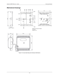
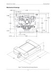
RedLab 1208FS-Plus User's Guide Functional Details Mechanical drawings Figure 15. Circuit board (top) and enclosure dimensions 18 Chapter 4 Specifications All specifications are subject to change without notice. Typical for 25°C unless otherwise specified. Specifications in italic text are guaranteed by design. Analog input Table 1. Analog input specifications Parameter Condition A/D converter type Input voltage range for linear operation CHx to GND Absolute maximum input voltage Input impedance Input current (Note 1) Number of channels Input ranges Throughput (Note 2) Specification CHx to GND Vin = +10 V Vin = 0 V Vin = –10 V Single-ended Differential Software paced Hardware paced Channel gain queue Resolution (Note 3) Differential Single-ended Integral linearity error Differential linearity error Repeatability Trigger source Software-selectable Pacer source Software-selectable Successive approximation type Single-ended mode: ±10 V max Differential mode: –10 V min, +20 V max ±28 V max 122 kΩ 70 µA typ –12 µA typ –94 µA typ 8 single-ended or 4 differential; software-selectable ±10 V, G=2 ±20 V, G=1 ±10 V, G=2 ±5 V, G=4 ±4 V, G=5 ±2.5 V, G=8 ±2.0 V, G=10 ±1.25 V, G=16 ±1.0 V, G=20 Software-selectable 250 S/s typ, PC-dependent 0.014 S/s to 50 kS/s Software selectable. 8 elements in SE mode, 4 elements in DIFF mode. One gain element per channel. Elements must be unique and listed in ascending order. 12 bits, no missing codes 11 bits ±1 LSB typ ±0.5 LSB typ ±1 LSB typ External digital: TRIG_IN Software-selectable Internal External (SYNC), rising edge triggered Software-selectable Note 1: Input current is a function of applied voltage on the analog input channels. For a given input voltage, Vin, the input leakage is approximately equal to (8.181 * Vin – 12) µA. Note 2: Maximum throughput when scanning is machine dependent. Note 3: The AD7870 converter only returns 11 bits (0 to 2,047 codes) in single-ended mode. 19 RedLab 1208FS-Plus User's Guide Specifications Accuracy Table 2. Accuracy, differential mode Range Accuracy (LSB) ±20 V ±10 V ±5 V ±4 V ±2.5 V ±2 V ±1.25 V ±1 V 5.1 6.1 8.1 9.1 12.1 14.1 20.1 24.1 Table 3. Accuracy, single-ended mode Range Accuracy (LSB) ±10 V 4.0 Table 4. Accuracy components, differential mode – all values are (±) Range % of Reading Gain Error at FS (mV) Offset (mV) Accuracy at FS (mV) ±20 V ±10 V ±5 V ±4 V ±2.5 V ±2 V ±1.25 V ±1 V 0.2 0.2 0.2 0.2 0.2 0.2 0.2 0.2 40 20 10 8 5 4 2.5 2 9.766 9.766 9.766 9.766 9.766 9.766 9.766 9.766 49.766 29.766 19.766 17.766 14.766 13.766 12.266 11.766 Table 5. Accuracy components, single-ended mode – all values are (±) Range % of Reading Gain Error at FS (mV) Offset (mV) Accuracy at FS (mV) ±10 V 0.2 20 19.531 39.531 Noise performance Table 6. Noise performance, differential mode Range Typical counts LSBrms ±20 V ±10 V ±5 V ±4 V ±2.5 V ±2 V ±1.25 V ±1 V 2 2 3 3 4 5 7 8 0.30 0.30 0.45 0.45 0.61 0.76 1.06 1.21 Table 7. Noise performance, single-ended mode Range Typical counts LSBrms ±10 V 2 0.30 20 RedLab 1208FS-Plus User's Guide Specifications Analog output Table 8. Analog output specifications Parameter Resolution Output range Number of channels Throughput (Note 4) Power on and reset voltage Output drive Slew rate Condition Specification Software paced Hardware paced 12-bits, 1 in 4,096 0 V to 5.0 V 2 250 S/s single channel typ, PC dependent 50 kS/s max per channel Initializes to 000h code 5 mA, sourcing 0.8 V/ µs typ Each D/A OUT Note 4: Maximum throughput when scanning is machine dependent. Table 9. Analog output accuracy, all values are (±); accuracy tested at no load Range Accuracy (LSB) 0 V to 5.0 V 4.0 typ, 45.0 max Table 10. Analog output accuracy components, all values are (±) Range % of FSR Gain Error at FS (mV) 0 V to 5.0 V 0.1 typ, 0.9 max 4.0 typ, 36.0 max Offset (mV) (Note 5) 1.0 typ, 9.0 max Accuracy at FS (mV) 4.0 typ, 45.0 max Note 5: Zero-scale offsets may result in a fixed zero-scale error producing a "dead-band” digital input code region. In this case, changes in digital input code at values less than 0x040 may not produce a corresponding change in the output voltage. The offset error is tested and specified at code 0x040. Digital input/output Table 11. Digital I/O specifications Parameter Specification Digital type Number of I/O Configuration Pull up/pull-down configuration CMOS 16 (Port A0 through A7, Port B0 through B7) 2 banks of 8. Port B is high current drive. All pins pulled up to 5V via 47 kΩ resistors (default). Change to pull-down using internal user-configurable jumpers. 2.0 V min 5.5 V absolute max 0.8 V max –0.5 V absolute min 0 V recommended min 4.4 V min (IOH = –20 µA) 3.84 V min (IOH = –6.0 mA) 0.1 V max (IOL = 20 µA) 0.33 V max (IOL = 6.0 mA) 4.4 V min (IOH = –50 µA) 3.76 V min (IOH = –24.0 mA) 0.1 V max (IOH = 50 µA) 0.44 V max (IOH = 24.0 mA) Input Input high voltage threshold Input high voltage limit Input low voltage threshold Input low voltage limit Output high voltage, Port A Output low voltage, Port A Output high voltage, Port B Output low voltage, Port B Power on and reset state 21 RedLab 1208FS-Plus User's Guide Specifications External trigger Table 12. Digital trigger specifications Parameter Specification Trigger source (Note 7) Trigger mode External digital; TRIG_IN terminal Edge sensitive; software-selectable for CMOS compatible rising or falling edge, high or low level. 10 µs max 1 µs min Schmitt trigger, 47 kΩ pull-down to ground 1.01 V typ 0.6 V min 1.5 V max 2.43 V typ 1.9 V min 3.1 V max 5.5 V absolute max 1.42 V typ 1.0 V min 2.0 V max –0.5 V absolute min 0 V recommended min Trigger latency Trigger pulse width Input type Schmitt trigger hysteresis Input high voltage threshold Input high voltage limit Input low voltage threshold Input low voltage limit External clock input/output Table 13. External clock I/O specifications Parameter Terminal name Terminal type Direction (software-selectable) Input clock rate Clock pulse width Condition Specification SYNC Bidirectional Outputs the internal A/D pacer clock Receives A/D pacer clock from external source 50 kHz, max 1 µs min 5 µs min Schmitt trigger, 47 kΩ pull-down to ground 1.01 V typ 0.6 V min 1.5 V max 2.43 V typ 1.9 V min 3.1 V max 5.5 V absolute max 1.42 V typ 1.0 V min 2.0 V max –0.5 V absolute min 0 V recommended min 4.4 V min (IOH = –50 µA) 3.80 V min (IOH = –8 mA) 0.1 V max (IOL = 50 µA) 0.44 V max (IOL = 8 mA) Output Input (default) Input mode Output mode Input type Schmitt trigger hysteresis Input high voltage threshold Input high voltage limit Input low voltage threshold Input low voltage limit Output high voltage Output low voltage 22 RedLab 1208FS-Plus User's Guide Specifications Counter Table 14. Counter specifications Parameter Specification Pin name Counter type Number of channels Input type Input source Resolution Maximum input frequency High pulse width Low pulse width Schmitt trigger hysteresis CTR Event counter 1 Schmitt trigger, 47 kΩ pull-down to ground, rising edge triggered CTR screw terminal 32 bits 1 MHz 500 ns min 500 ns min 1.01 V typ 0.6 V min 1.5 V max 2.43 V typ 1.9 V min 3.1V max 5.5 V absolute max 1.42 V typ 1.0 V min 2.0 V max –0.5 V absolute min 0 V recommended min Input high voltage threshold Input high voltage limit Input low voltage threshold Input low voltage limit Memory Table 15. Memory specifications Non-volatile EEPROM 2,048 bytes (768 bytes calibration, 256 bytes user, 1,024 bytes DAQFlex) Microcontroller Table 16. Microcontroller specifications Type High performance 16-bit RISC microcontroller Power Table 17. Power specifications Parameter Condition Specification Supply current During USB enumeration After USB enumeration, including DIO, AO, SYNC, and +VO output loading After USB enumeration After USB enumeration < 100 mA < 500 mA +VO power available +VO output current 23 4.5 V min, 5.25 V max 100 mA max RedLab 1208FS-Plus User's Guide Specifications General Table 18. General specifications Parameter Specification Device type Device compatibility USB 2.0 full speed USB 1.1, USB 2.0 Environmental Table 19. Environmental specifications Parameter Specification Operating temperature range Storage temperature range Humidity 0 °C to 70 °C –40 °C to 70 °C 0% to 90% non-condensing Mechanical Table 20. Mechanical specifications Parameter Specification Dimensions (L × W × H) USB cable length User connection length 79 × 82 × 27 mm (3.10 × 3.20 × 1.05 in.) 3 m (9.84 ft) max 3 m (9.84 ft) max Signal connector Table 21. Screw terminal specifications Parameter Specification Connector type Wire gauge range Screw terminal 16 AWG to 30 AWG 24 RedLab 1208FS-Plus User's Guide Specifications Differential mode pinout Table 22. 4-channel differential mode pinout Pin 1 2 3 4 5 6 7 8 9 10 11 12 13 14 15 16 17 18 19 20 Signal name CH0 IN HI CH0 IN LO AGND CH1 IN HI CH1 IN LO AGND CH2 IN HI CH2 IN LO AGND CH3 IN HI CH3 IN LO AGND D/A OUT 0 D/A OUT 1 AGND Reserved GND TRIG_IN SYNC CTR Pin description Analog input 0+ Analog input 0– Analog ground Analog input 1+ Analog input 1– Analog ground Analog input 2+ Analog input 2– Analog ground Analog input 3+ Analog input 3– Analog ground Analog output 0 Analog output 1 Analog ground Reserved for future use Ground Trigger input Synchronization I/O Counter input Pin 21 22 23 24 25 26 27 28 29 30 31 32 33 34 35 36 37 38 39 40 Signal name Port A0 Port A1 Port A2 Port A3 Port A4 Port A5 Port A6 Port A7 GND +VO GND Port B0 Port B1 Port B2 Port B3 Port B4 Port B5 Port B6 Port B7 GND Pin description Port A bit 0 Port A bit 1 Port A bit 2 Port A bit 3 Port A bit 4 Port A bit 5 Port A bit 6 Port A bit 7 Ground Power output Ground Port B bit 0 Port B bit 1 Port B bit 2 Port B bit 3 Port B bit 4 Port B bit 5 Port B bit 6 Port B bit 7 Ground Single-ended mode pinout Table 23. 8-channel single-ended mode pinout Pin 1 2 3 4 5 6 7 8 9 10 11 12 13 14 15 16 17 18 19 20 Signal name CH0 IN CH1 IN AGND CH2 IN CH3 IN AGND CH4 IN CH5 IN AGND CH6 IN CH7 IN AGND D/A OUT 0 D/A OUT 1 AGND Reserved GND TRIG_IN SYNC CTR Pin description Analog input 0 Analog input 1 Analog ground Analog input 2 Analog input 3 Analog ground Analog input 4 Analog input 5 Analog ground Analog input 6 Analog input 7 Analog ground Analog output 0 Analog output 1 Analog ground Reserved for future use Ground Trigger input Synchronization I/O Counter input Pin 21 22 23 24 25 26 27 28 29 30 31 32 33 34 35 36 37 38 39 40 25 Signal name Port A0 Port A1 Port A2 Port A3 Port A4 Port A5 Port A6 Port A7 GND +VO GND Port B0 Port B1 Port B2 Port B3 Port B4 Port B5 Port B6 Port B7 GND Pin description Port A bit 0 Port A bit 1 Port A bit 2 Port A bit 3 Port A bit 4 Port A bit 5 Port A bit 6 Port A bit 7 Ground Power output Ground Port B bit 0 Port B bit 1 Port B bit 2 Port B bit 3 Port B bit 4 Port B bit 5 Port B bit 6 Port B bit 7 Ground Meilhaus Electronic GmbH Am Sonnenlichte 2 D-82239 Alling, Germany Phone: +49 (0)81 41 - 52 71-0 Fax: +49 (0)81 41 - 52 71-129 E-Mail: [email protected] http://www.meilhaus.com