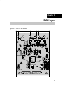
1
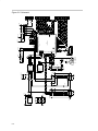
! "#$ # % &' User’s Guide September 2001 Mixed Signal Products SLVU050 IMPORTANT NOTICE Texas Instruments Incorporated and its subsidiaries (TI) reserve the right to make corrections, modifications, enhancements, improvements, and other changes to its products and services at any time and to discontinue any product or service without notice. Customers should obtain the latest relevant information before placing orders and should verify that such information is current and complete. All products are sold subject to TI’s terms and conditions of sale supplied at the time of order acknowledgment. TI warrants performance of its hardware products to the specifications applicable at the time of sale in accordance with TI’s standard warranty. Testing and other quality control techniques are used to the extent TI deems necessary to support this warranty. Except where mandated by government requirements, testing of all parameters of each product is not necessarily performed. TI assumes no liability for applications assistance or customer product design. Customers are responsible for their products and applications using TI components. To minimize the risks associated with customer products and applications, customers should provide adequate design and operating safeguards. TI does not warrant or represent that any license, either express or implied, is granted under any TI patent right, copyright, mask work right, or other TI intellectual property right relating to any combination, machine, or process in which TI products or services are used. Information published by TI regarding third–party products or services does not constitute a license from TI to use such products or services or a warranty or endorsement thereof. Use of such information may require a license from a third party under the patents or other intellectual property of the third party, or a license from TI under the patents or other intellectual property of TI. Reproduction of information in TI data books or data sheets is permissible only if reproduction is without alteration and is accompanied by all associated warranties, conditions, limitations, and notices. Reproduction of this information with alteration is an unfair and deceptive business practice. TI is not responsible or liable for such altered documentation. Resale of TI products or services with statements different from or beyond the parameters stated by TI for that product or service voids all express and any implied warranties for the associated TI product or service and is an unfair and deceptive business practice. TI is not responsible or liable for any such statements. Mailing Address: Texas Instruments Post Office Box 655303 Dallas, Texas 75265 Copyright 2001, Texas Instruments Incorporated EVM IMPORTANT NOTICE Texas Instruments (TI) provides the enclosed product(s) under the following conditions: This evaluation kit being sold by TI is intended for use for ENGINEERING DEVELOPMENT OR EVALUATION PURPOSES ONLY and is not considered by TI to be fit for commercial use. As such, the goods being provided may not be complete in terms of required design-, marketing-, and/or manufacturing-related protective considerations, including product safety measures typically found in the end product incorporating the goods. As a prototype, this product does not fall within the scope of the European Union directive on electromagnetic compatibility and therefore may not meet the technical requirements of the directive. Should this evaluation kit not meet the specifications indicated in the EVM User’s Guide, the kit may be returned within 30 days from the date of delivery for a full refund. THE FOREGOING WARRANTY IS THE EXCLUSIVE WARRANTY MADE BY SELLER TO BUYER AND IS IN LIEU OF ALL OTHER WARRANTIES, EXPRESSED, IMPLIED, OR STATUTORY, INCLUDING ANY WARRANTY OF MERCHANTABILITY OR FITNESS FOR ANY PARTICULAR PURPOSE. The user assumes all responsibility and liability for proper and safe handling of the goods. Further, the user indemnifies TI from all claims arising from the handling or use of the goods. Please be aware that the products received may not be regulatory compliant or agency certified (FCC, UL, CE, etc.). Due to the open construction of the product, it is the user’s responsibility to take any and all appropriate precautions with regard to electrostatic discharge. EXCEPT TO THE EXTENT OF THE INDEMNITY SET FORTH ABOVE, NEITHER PARTY SHALL BE LIABLE TO THE OTHER FOR ANY INDIRECT, SPECIAL, INCIDENTAL, OR CONSEQUENTIAL DAMAGES. TI currently deals with a variety of customers for products, and therefore our arrangement with the user is not exclusive. TI assumes no liability for applications assistance, customer product design, software performance, or infringement of patents or services described herein. Please read the EVM User’s Guide and, specifically, the EVM Warnings and Restrictions notice in the EVM User’s Guide prior to handling the product. This notice contains important safety information about temperatures and voltages. For further safety concerns, please contact the TI application engineer. Persons handling the product must have electronics training and observe good laboratory practice standards. No license is granted under any patent right or other intellectual property right of TI covering or relating to any machine, process, or combination in which such TI products or services might be or are used. Mailing Address: Texas Instruments Post Office Box 655303 Dallas, Texas 75265 Copyright 2001, Texas Instruments Incorporated EVM WARNINGS AND RESTRICTIONS It is important to operate this EVM within the specified input and output ranges described in the EVM User’s Guide. Exceeding the specified input range may cause unexpected operation and/or irreversible damage to the EVM. If there are questions concerning the input range, please contact a TI field representative prior to connecting the input power. Applying loads outside of the specified output range may result in unintended operation and/or possible permanent damage to the EVM. Please consult the EVM User’s Guide prior to connecting any load to the EVM output. If there is uncertainty as to the load specification, please contact a TI field representative. During normal operation, some circuit components may have case temperatures greater than 60°C. The EVM is designed to operate properly with certain components above 60°C as long as the input and output ranges are maintained. These components include but are not limited to linear regulators, switching transistors, pass transistors, and current sense resistors. These types of devices can be identified using the EVM schematic located in the EVM User’s Guide. When placing measurement probes near these devices during operation, please be aware that these devices may be very warm to the touch. Mailing Address: Texas Instruments Post Office Box 655303 Dallas, Texas 75265 Copyright 2001, Texas Instruments Incorporated Related Documentation From Texas Instruments Preface Read This First How to Use This Manual This document contains the following chapters: - Chapter 1 – Introduction - Chapter 2 – Hardware Overview - Chapter 3 – EVM Operation - Chapter 4 – Bill of Materials - Chapter 5 – EVM Layout Related Documentation From Texas Instruments TPS2149 3.3-V LDO and Dual Switch data sheet, literature number SLVS401. TUSB2136 USB Keyboard Hub Controller data sheet, literature number SLLS442. FCC Warning This equipment is intended for use in a laboratory test environment only. It generates, uses, and can radiate radio frequency energy and has not been tested for compliance with the limits of computing devices pursuant to subpart J of part 15 of FCC rules, which are designed to provide reasonable protection against radio frequency interference. Operation of this equipment in other environments may cause interference with radio communications, in which case the user at his own expense will be required to take whatever measures may be required to correct this interference. v vi Contents Contents 1 Introduction . . . . . . . . . . . . . . . . . . . . . . . . . . . . . . . . . . . . . . . . . . . . . . . . . . . . . . . . . . . . . . . . . . . . . 1-1 1.1 Required Hardware and Software . . . . . . . . . . . . . . . . . . . . . . . . . . . . . . . . . . . . . . . . . . . . . 1-2 2 Hardware Overview . . . . . . . . . . . . . . . . . . . . . . . . . . . . . . . . . . . . . . . . . . . . . . . . . . . . . . . . . . . . . . 2-1 3 EVM Operation . . . . . . . . . . . . . . . . . . . . . . . . . . . . . . . . . . . . . . . . . . . . . . . . . . . . . . . . . . . . . . . . . . 3.1 TPS2149 Setup . . . . . . . . . . . . . . . . . . . . . . . . . . . . . . . . . . . . . . . . . . . . . . . . . . . . . . . . . . . . 3.2 Interfaces and USB Ports . . . . . . . . . . . . . . . . . . . . . . . . . . . . . . . . . . . . . . . . . . . . . . . . . . . . 3.3 Power Supplies . . . . . . . . . . . . . . . . . . . . . . . . . . . . . . . . . . . . . . . . . . . . . . . . . . . . . . . . . . . . . 3.4 Light Emitting Diodes (LEDs) . . . . . . . . . . . . . . . . . . . . . . . . . . . . . . . . . . . . . . . . . . . . . . . . . 3.5 Jumpers and Test Points . . . . . . . . . . . . . . . . . . . . . . . . . . . . . . . . . . . . . . . . . . . . . . . . . . . . 3.6 EEPROM . . . . . . . . . . . . . . . . . . . . . . . . . . . . . . . . . . . . . . . . . . . . . . . . . . . . . . . . . . . . . . . . . . 4 Bill of Materials . . . . . . . . . . . . . . . . . . . . . . . . . . . . . . . . . . . . . . . . . . . . . . . . . . . . . . . . . . . . . . . . . . 4-1 5 EVM Layout . . . . . . . . . . . . . . . . . . . . . . . . . . . . . . . . . . . . . . . . . . . . . . . . . . . . . . . . . . . . . . . . . . . . . 5-1 3-1 3-2 3-2 3-2 3-2 3-3 3-3 Figures 1–1 5–1 5–2 USB Keyboard/Hub EVM Hardware . . . . . . . . . . . . . . . . . . . . . . . . . . . . . . . . . . . . . . . . . . . . . 1-2 TPS2149 Silk Screen . . . . . . . . . . . . . . . . . . . . . . . . . . . . . . . . . . . . . . . . . . . . . . . . . . . . . . . . . . 5-1 Schematic . . . . . . . . . . . . . . . . . . . . . . . . . . . . . . . . . . . . . . . . . . . . . . . . . . . . . . . . . . . . . . . . . . . 5-2 Tables 3–1 3–2 3–3 4–1 LED Description . . . . . . . . . . . . . . . . . . . . . . . . . . . . . . . . . . . . . . . . . . . . . . . . . . . . . . . . . . . . . . Jumpers and Test Points . . . . . . . . . . . . . . . . . . . . . . . . . . . . . . . . . . . . . . . . . . . . . . . . . . . . . . . QWERTY Keyboard Matrix . . . . . . . . . . . . . . . . . . . . . . . . . . . . . . . . . . . . . . . . . . . . . . . . . . . . . EVM Bill of Materials . . . . . . . . . . . . . . . . . . . . . . . . . . . . . . . . . . . . . . . . . . . . . . . . . . . . . . . . . . 3-2 3-3 3-3 4-1 vii viii Chapter 1 Introduction This user’s guide describes the setup and operation of the USB keyboard/hub evaluation module (EVM). Information and instruction presented throughout this document assumes user familiarity with universal serial bus (USB) protocol and the use of common lab testing equipment. Topic 1.1 Page Required Hardware and Software . . . . . . . . . . . . . . . . . . . . . . . . . . . . . . 1-2 1-1 Required Hardware and Software 1.1 Required Hardware and Software The USB keyboard/hub EVM is designed for use with a personal computer running a USB-enabled operating system. The PC, with BIOS, chipsets, and operating system, should be USB 1.1 specification-compliant. If the BIOS is not compliant, the system may not boot when USB devices are connected at power up, and the EVM may not function in DOS mode. Additionally, one or more USB devices are needed to plug into the downstream ports of the USB keyboard/hub EVM to exercise the hub ports. A standard USB cable is needed to connect the USB keyboard/hub EVM to a downstream port of the PC or a USB hub tier. Figure 1–1. USB Keyboard/Hub EVM Hardware USB EVM 1-2 Chapter 2 Hardware Overview The USB keyboard/hub EVM is 4-inches L × 3.5-inches W and features the TPS2149 made by Texas Instruments. The TPS2149 is a power management device that integrates an LDO and two power switches into one small package. Jumpers (0-Ω resistors) and jumper blocks provided on the EVM are installed with the factory settings. The settings are described in Table 3–2. Review all setting changes prior to powering the EVM. Improper settings could result in damage to some of the EVM components. The factory settings allow the EVM to operate using a 12-MHz crystal along with an I2C EEPROM. The EVM has also been configured to work only in bus-powered mode. The firmware installed at the factory and stored in the EEPROM will allow the EVM to function as a two port keyboard hub. Users are responsible for developing their own application firmware for the target hardware device. The EVM also uses a TUSB2136, USB keyboard/hub controller, made by Texas Instruments, to communicate with the host and the downstream devices. A USB cable is needed to connect the root hub of the PC to the EVM type B connector (J5). The downstream devices connect to the EVM via the J6 and J7 connectors. These downstream devices are powered through the TPS2149. The USB specifications require that downstream ports remain off until enumeration is complete. Together, the TUSB2136 and the TPS2149 ensure the hub meets this requirement. Two other connectors, J3 and J4, allow easy connection to the TUSB2136 general-purpose I/O lines. These lines can be used to implement the keyboard function. Jumpers, test points, and LEDs have been added for testing, troubleshooting and debugging purposes. Most of the test points are located near the TPS2149. There are also test points on the differential pair lines of the upstream B-type connector and the two downstream A-type connectors. The I2C port can be probed directly on the EEPROM. Six LEDs are provided for quick feedback during firmware debugging or as status information. One LED (D1) is fixed to provide power and suspend status of the TUSB2136 device. Hardware Overview 2-1 2-2 Chapter 3 EVM Operation Operation of the USB keyboard/hub EVM is summarized in paragraphs 3.1 through 3.6. Topic Page 3.1 TPS2149 Setup . . . . . . . . . . . . . . . . . . . . . . . . . . . . . . . . . . . . . . . . . . . . . . . 3-2 3.2 Interfaces and USB Ports . . . . . . . . . . . . . . . . . . . . . . . . . . . . . . . . . . . . . . 3-2 3.3 Power Supplies . . . . . . . . . . . . . . . . . . . . . . . . . . . . . . . . . . . . . . . . . . . . . . 3-2 3.4 Light-Emitting Diodes (LEDs) . . . . . . . . . . . . . . . . . . . . . . . . . . . . . . . . . . 3-2 3.5 Jumpers and Test Points . . . . . . . . . . . . . . . . . . . . . . . . . . . . . . . . . . . . . . 3-3 3.6 EEPROM . . . . . . . . . . . . . . . . . . . . . . . . . . . . . . . . . . . . . . . . . . . . . . . . . . . . . 3-3 EVM Operation 3-1 TPS2149 Setup 3.1 TPS2149 Setup The USB keyboard/hub EVM is designed to allow evaluation of the TPS2149 device. Test points and 0-Ω resistors are provided to simplify the evaluation process (see Section 3.5). The EVM comes in a default configuration that requires no additional components, other than the required hardware and software identified in Section 1.1 of this user’s guide. For a complete description of the TPS2149 device, consult the TPS2149 data sheet (literature number SLVS401). 3.2 Interfaces and USB Ports The EVM uses a standard Type-B connector for the upstream port and two single Type A connectors for the downstream ports. Power to the downstream ports is provided throught the TPS2149. Two edge connectors, J3 and J4, connect to the TUSB2136 general-purpose I/O lines. Out of 32 general-purpose I/O lines, 26 are brought out to the J3 and J4 connectors. The remaining 6 I/O lines are used onboard to control the LEDs (see Section 3.4). 3.3 Power Supplies The USB keyboard/hub EVM requires no external power supply for operation. The EVM receives power via the USB cable. The TPS2149 low-dropout regulator is used to generate the required 3.3-V supply from the USB 5-V supply. The power indicator LED (D1) will turn on whenever power is available to the EVM (see Table 3–1). 3.4 Light Emitting Diodes (LEDs) Several onboard LEDs are provided on the EVM for quick and easy evaluation. A set of six green LEDs (D2 – D7), connected to P3.0 through P3.5 of the TUSB2136, may be used for general purposes in any code that is written for the TUSB2136 (see Table 3–1). By default, the factory code provides the EVM with the use of only three of the LEDs as keyboard status indicators for Scroll Lock (D2), Caps Lock (D3), and Num Lock (D4). The other three are not used. Table 3–1. LED Description LED Description D2–D7 Green LED ON indicates corresponding GPIO pin is low (when D1 is ON). Green LED OFF indicates corresponding GPIO pin is high (when D1 is ON). D1 Red LED ON indicates that the EVM is powered on and not suspended. Red LED OFF indicates that the EVM is powered off or suspended. 3-2 Jumpers and Test Points 3.5 Jumpers and Test Points Table 3–2 describes the jumpers, J1 and J2, used to connect P3.0 and P3.1 to D6 and D7 respectively, which should only be done when P3.0/S0 and P3.1/S1 are not set to GND for VID/PID selection (see the TUSB2136 keyboard hub controller data sheet). Table 3–2 also describes the various 0-Ω resistors used as jumpers. Test points are located throughout the EVM. For location of these test points, consult the layout in Section 5. Table 3–2. Jumpers and Test Points Jumpers Description J1 Installed: connects P3.1 to D7 J2 Installed: connects P3.0 to D6 0-Ω resistors used to configure the TUSB2136. For proper operation with the firmware and EVM, R30, R31, and R33 are installed at the factory. R30 thru R35 R29, R36, R37, R38 0-Ω resistors on power lines which may be removed to insert a current meter. 3.6 EEPROM The EEPROM is used for application-specific firmware. The TUSB2136 will automatically read the EEPROM at power up via the I2C bus. A header must be added to the application firmware before loading into the EEPROM. This header format is specified in the bootcode document provided with the TUSB2136. The header may be generated automatically with the I2C header generation utility software also provided with the TUSB2136. For convenience, the EEPROM has been installed on a socket. If desired, the socket may be removed and the EEPROM can be soldered directly onto the board. Using J3 and J4, the firmware installed at the factory will support a QWERTY keyboard with the matrix shown in Table 3–3. Table 3–3. QWERTY Keyboard Matrix Port No. Matrix P3.6 COL 1 P0.6 COL 2 P0.7 COL 3 P0.4 COL 4 P0.5 COL 5 P0.2 COL 6 P0.3 COL 7 P2.7 ROW 1 Q 9 A 6 Z 3 DEL P2.6 ROW 2 W 8 S 5 X 2 0 P2.5 ROW 3 E 7 D 4 C 1 INS P2.4 ROW 4 R ESC F HOME V END R ARROW P2.3 ROW 5 T I G K B / SPACE P2.2 ROW 6 Y P H “ N U ARROW D ARROW P2.1 ROW 7 U O J L M \ L ARROW P2.0 ROW 8 – , + ENTER . P0.0 COL 8 P0.1 COL 9 P1.6 COL 10 SHIFT ALT CTL EVM Operation 3-3 3-4 Chapter 4 Bill of Materials Table 4–1. EVM Bill of Materials Item Qty Ref. Des. Footprint MFR Part Number Description 1 1 U1 PKG_8P_DGK8 TI TPS2149 3.3-V LDO and dual switch 2 1 U2 PKG_5P_SOT23 TI TPS77018DBVR LDO 1.8 V output 3 1 U4 TUSB2136PM TI TUSB2136PM IC, 2 PORT USB HUB with FUN CONTR, 64 pin 4 4 FB1, FB2, FB3, FB4 1812 Mouser 623-2743019447 Ferrite bead 5 10 C3, C5, C11–C14, C17–C20 C0805 KEMET C0805C104K5RAC7800 Capacitor, ceramic, 0.1-µF, 50 V, X7R, 10% 6 1 C6 C0805 Murata GRM40X7R105K16PT Capacitor, ceramic, 1.0-µF, 16 V, 20% 7 4 C7–C10 C0605 Murate GRM39C0G220J050AD Capacitor, ceramic, 22-pF, 50 V, 5% 8 2 C1, C2 C0605 Murata GRM39C0G330J050AD Capacitor, ceramic, 33 pF, 16 V, 20% 9 2 C15, C16 7343D NEMCO LSR100/16DK125 Capacitor, tantalum, 100 µF, 16 V, 20% 10 1 C4 CAP_TANTALUM_B Sprague 293D475X0010B2T Capacitor, tantalum, 4.7 µF, 10 V, 20% 11 2 J6, J7 CONN_USB_A Digi-Key AU-Y1005 Connector, USB downstream (Type A) 12 1 J5 CONN_USB_B Digi-Key AU-Y1007 Connector, USB upstream (Type B) 13 1 X1 CRYSTAL_016695 Crytek 16695 Crystal, 12 MHz, 20 pF, ±50 PPM at 25°C 14 6 D2–D7 D-LTST-C170FKT Liteon LTST-C170FKT Diode, LED, green, 2.1 V, 14.2-mcd, 20 Ma, 0805 15 1 D1 D-LTST-C170UKT Liteon LTST-C170UKT Diode, LED, red, 2.1 V, 14.2-mcd, 20 Ma, 0805 16 2 J1, J2 HEADER_1X2 Digi-Key S1012-36-ND Header, 2 pin, 100 mil spacing, 36-pin strip 17 2 J3, J4 HEADER_2X7 Samtec SSW-107-02-T-D-RA Header, 2x7 RT ANG. pin, 100 mil 18 4 R9, R12–R14 R0805 Std Std Resistor, chip, 15 kΩ, 1/10 W, 5% Bill of Materials 4-1 Table 4–1. EVM Bill of Materials (Continued) Item Qty Ref. Des. Footprint MFR Part Number Description 19 10 R29–R38 R0805 Std Std Resistor, chip, 0 Ω, 1/10 W, 5% 20 2 R15, R17 R0805 Std Std Resistor, chip, 1 kΩ, 1/10 W, 5% 21 2 R16, R25 R0805 Std Std Resistor, chip, 1.5 kΩ, 1/10 W, 5% 22 1 R24 R0805 Std Std Resistor, chip, 10 Ω, 1/10 W, 5% 23 2 R20, R21 R0805 Std Std Resistor, chip, 20 kΩ, 1/10 W, 5% 24 6 R10, R11, R18, R19, R22, R26 R0805 Std Std Resistor, chip, 30 Ω, 1/10 W, 5% 25 2 R27, R28 R0805 Std Std Resistor, chip, 30.1 kΩ, 1/10 W, 5% 26 1 R23 R0805 Std Std Resistor, chip, 200 kΩ, 1/10 W, 5% 27 8 R1–R8 R0805 Std Std Resistor, chip, 511 Ω, 1/10 W, 5% 28 1 XU1 8 DIP Digi-Key 24LC64P IC serial EEPROM 8K x 8 2.5 V 29 1 XU1 8 pin socket Digi-Key 110-99-308-41-001 IC socket 8 pin MS Tin/ Tin.300 30 1 S1 NC Digi-Key P80075-ND Switch, 1P1T, 20 mA, 15 V 31 18 TP7–TP13, TP15–25 TP_RED_1MM Farnell 240-345 Test pint, red, 1 mm 32 1 TP14 TP_BLACK_1MM Farnell 240-333 Test pint, black, 1 mm 33 1 Q1 SOT-23 On Semi TR-MMBT3906LT1 Bipolar, PNP, 40 V, 350 mA, zz W 4-2 Chapter 5 EVM Layout Figure 5–1. TPS2149 Silk Screen EVM Layout 5-1 DGND 1.8 V 0.1 µ F 0.1 µ F 0.1 µ F 0.1 µ F C14 C17 C18 C19 DGND 0.1 µ F 0.1 µ F C13 C20 0.1 µ F C12 U2 C6 0.1 µ F J6 FB1 C7 22 pF DVCC_33 DVCC_33 Case 5 GND 2 1.8 V GND LDO 1 15 kΩ 30 Ω 30 Ω R9 4 3 V– NC + C15 100 µF FB2 R12 15 kΩ Case C8 22 pF FB4 R18 30 Ω 0Ω 0Ω 0Ω 100 µF J7 C9 R13 22 pF R14 R19 15 kΩ 15 kΩ 30 Ω R36 R29 R37 C3 + C16 100 µF FB3 OC GND LDO_OUT OUT2 DVCC_33 DGND S3 DGND 2A 1A R24 10 Ω S1 33 SUSP R17 S2 P3.0 P3.1 R27 30.1 kΩ 33 SUSP 4B DGND 3B 6 7 4 5 3 1 2 13 14 15 16 8 9 10 11 12 PWR02 PWR01 OVCR1 GND DM1 DP1 OCYR2 TEST1 SUSP RST TEST0 SCL S3 VCC SDA S2 DVCC_33 R8 R6 R5 R4 33 SUSP Q1 511 Ω 511 Ω 511 Ω 511 Ω TUSB2136PM U4 R26 30 Ω R25 1.5 KΩ R38 0Ω 30 R22 J5 17 18 19 20 21 22 23 24 25 26 27 28 29 30 31 32 36 P1.5 35 P1.4 34 P1.3 33 P1.2 48 P0.5 P0.4 47 P0.3 46 45 P0.2 P0.1 44 43 P0.0 42 GND 41 P1.7 P1.6 40 39 VCC 38 VREN VDDOUT 37 R16 D4 511 Ω R2 D3 511 Ω R1 D2 DVCC_33 64 63 62 61 60 59 58 47 56 55 54 53 52 51 50 49 33 pF DGND SUSP S2 S3 DVCC_33 DGND DGND 33 SUSP DGND X1 12 MHz OSC R20 20 kΩ R21 20 kΩ 1 kΩ 5 6 7 1 kΩ GND 8 5 6 7 8 R15 DVCC_33 GND GND GND XU1 EEPROM EN2 EN1 VIN OUT1 GND C11 0.1 µ F C10 22 pF DGND 4 3 2 1 DGND 4 3 2 1 U1 33 pF DP2 3 V+ C2 Case 4 3 V– R10 R11 2 1 DP DM VCC DM0 GND V+ Power 2 1 DP DM 4 Case X1 X2 4.7 µF V+ P3.2 C4 + 1 2 DM DP P3.0/S0 P2.1 0.1 µF C5 Case DM2 PUR DP0 P3.3 DGND 3 4 V– P3.1 P3.1/S1 GND P2.2 DGND 200 k Ω DGND P3.0 GND SELF/BUS P2.0 Case R23 P3.4 P3.5 P2.3 P2.4 Power R30 0 Ω P3.6 P2.5 DGND R31 0 Ω R32 0 Ω P3.7 P2.6 DGND R33 0 Ω R34 0 Ω R35 0 Ω P0.7 P0.6 P2.7 P1.0 5-2 P1.1 C1 1.5 KΩ D5 D1 D7 DVCC_33 R7 R3 DVCC_33 1.8 V DGND D6 SUSP 2 2 1 9 8 7 6 5 4 3 2 10 11 14 13 12 1 9 8 7 6 5 4 3 2 10 11 14 13 12 511 Ω 1 P3.0 511 Ω 1 P3.1 J4 J3 J2 J1 Figure 5–2. Schematic