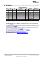
1
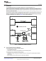
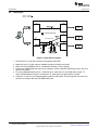
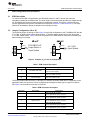
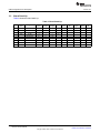
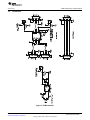
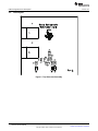
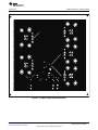
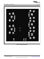
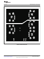
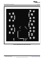
User's Guide
SCDU001A – July 2009 – Revised October 2009
TS3USB221/A/E High Speed USB 2.0 (480 Mbps) 1:2
Multiplexer/Demultiplexer Switch Evaluation Module
1
2
3
4
Contents
Preface ....................................................................................................................... 2
Introduction .................................................................................................................. 3
EVM Configuration and Description ...................................................................................... 5
Related Documentation ................................................................................................... 14
List of Figures
1
TS3USB221/A/E EVM Block Diagram ................................................................................... 3
2
Quick Start Evaluation ...................................................................................................... 4
3
Jumpers J6, J7, and J8 Configuration
4
EVM Schematic ............................................................................................................. 7
5
Top Silkscreen/Assembly .................................................................................................. 9
6
Top Metal (High-Speed Differential)
10
7
Internal Ground Plane
11
8
9
10
...................................................................................
....................................................................................
....................................................................................................
Internal Power Plane ......................................................................................................
Bottom Metal (Low-Speed Single-Ended) ..............................................................................
Bottom Silkscreen/Assembly .............................................................................................
5
12
13
13
List of Tables
1
EVM Jumper Description................................................................................................... 5
2
EVM Connector Description ............................................................................................... 5
3
Board Stack-Up
4
Bill of Materials............................................................................................................. 14
.............................................................................................................
SCDU001A – July 2009 – Revised October 2009
Submit Documentation Feedback
TS3USB221/A/E High Speed USB 2.0 (480 Mbps) 1:2 Multiplexer/Demultiplexer
Switch Evaluation Module
Copyright © 2009, Texas Instruments Incorporated
6
1
Preface
www.ti.com
1
Preface
1.1
About This Manual
This user’s guide describes the TS3USB221/A/E Evaluation Module (EVM). This guide contains the EVM
schematics, bill of materials, assembly drawings, and top and bottom board layouts.
1.2
How to Use This Manual
This document contains the following chapters:
• Chapter 1 – Preface
• Chapter 2 – Introduction and Quick Start
• Chapter 2 – EVM Configuration and Description
• Chapter 3 – Related Documents
1.2.1
Information about Cautions and Warnings
ATTENTION
STATIC SENSITIVE DEVICES
HANDLE ONLY AT
STATIC SAFE WORK STATIONS
CAUTION
This EVM contains components that can potentially be damaged by
electrostatic discharge. Always transport and store the EVM in its supplied ESD
bag when not in use. Handle using an antistatic wristband. Operate on an
antistatic work surface. For more information on proper handling, see the
Electrostatic Discharge (ESD) application note (SSYA008).
The information in a caution or a warning is provided for your protection. Please read each caution and
warning carefully.
1.2.2
FCC Warning
This equipment is intended for use in a laboratory test environment only. It generates, uses, and can
radiate radio frequency energy and has not been tested for compliance with the limits of computing
devices pursuant to subpart J of part 15 of FCC rules, which are designed to provide reasonable
protection against radio frequency interference. Operation of this equipment in other environments may
cause interference with radio communications, in which case the user at his/her own expense will be
required to take whatever measures may be required to correct this interference.
2
TS3USB221/A/E High Speed USB 2.0 (480 Mbps) 1:2 Multiplexer/Demultiplexer
Switch Evaluation Module
Copyright © 2009, Texas Instruments Incorporated
SCDU001A – July 2009 – Revised October 2009
Submit Documentation Feedback
Introduction
www.ti.com
2
Introduction
The TS3USB221/A/E EVM is an evaluation module for the Texas Instruments (TI) 1:2
multiplexer/demultiplexer high-bandwidth USB switches. It is specially designed for high-speed USB 2.0
signals, supports bidirectional signaling, and offers high-bandwidth (1.1 GHz). When interfacing other USB
devices with this EVM, the switch allows signals to pass with minimum edge and phase distortion as well
as little or no signal attenuation.
This evaluation module is designed to demonstrate the small printed circuit board (PCB) areas that can be
achieved when designing with the TS3USB221/A/E USB switches. It is powered from the 5-V rail of the
USB input. Additionally, the TS3USB221/A/E provides an output enable input and an output select input
for flexible configuration of the USB. See Figure 1 for the EVM block diagram.
TS3USB221/A/E EVM
TS3USB221/A/E
Figure 1. TS3USB221/A/E EVM Block Diagram
2.1
List of Hardware Items for Operation
The following items are required for EVM evaluation:
• The TS3USB221/A/E EVM
• USB cables with connector type depending on the surrounding system
The following items are optional for EVM evaluation:
• USB type A or type B connectors to change connectors J1 through J5 for optimal system interface
configuration
• IBM compatible PC with USB 2.0 ports for quick start evaluation
SCDU001A – July 2009 – Revised October 2009
Submit Documentation Feedback
TS3USB221/A/E High Speed USB 2.0 (480 Mbps) 1:2 Multiplexer/Demultiplexer
Switch Evaluation Module
Copyright © 2009, Texas Instruments Incorporated
3
Introduction
2.2
www.ti.com
Quick Start
TS3USB221/A/E EVM
TS3USB221/A/E
Figure 2. Quick Start Evaluation
1.
2.
3.
4.
Connect the PC to the USB connector J3 through a USB cable.
Make sure the 3.3-V LDO output is enabled by opening J8 without a jumper.
Make sure the TS3USB221/A/E IC is enabled by shunting J7 with a jumper.
Connect two USB downstream devices (for example, mouse, keyboard, USB memory stick, etc) to J4
and J5 on the EVM.
5. To select USB downstream device 1 connected to J4, make sure J6 is shunted with a jumper. To
select USB downstream device 2 connected to J5, make sure J6 is open without a jumper.
6. Connector J1 and J2 are connected together without a USB switch. This through-path can serve as a
reference to compare with the TS3USB221/A/E path.
4
TS3USB221/A/E High Speed USB 2.0 (480 Mbps) 1:2 Multiplexer/Demultiplexer
Switch Evaluation Module
Copyright © 2009, Texas Instruments Incorporated
SCDU001A – July 2009 – Revised October 2009
Submit Documentation Feedback
EVM Configuration and Description
www.ti.com
3
EVM Configuration and Description
3.1
EVM Description
To conform to the USB 2.0 specification, the differential traces D+ and D- lines on the board are
impedance matched to 90-Ω differential. The trace length of the through-path and the trace length through
the TS3USB221/A/E switch are also matched for comparison purpose. The PCB is a simple four-layer
top-side populated board (see the schematic and PCB layout in Section 3.4 and Section 3.5). The major
features of the hardware design are detailed in the following sections.
3.2
Jumper Configuration (J6 to J8)
The EVM has jumper J6 through J8 (see Figure 3) to provide configuration to the TS3USB221/A/E and the
3.3-V LDO. J6 allows switch output channel select, J7 provides switch enable control, and J8 provides
3.3-V LDO enable control. Table 1 lists all of the jumpers in the EVM and their respective functionality (all
default settings are in bold).
10 kW
TS3USB221/A/E
Output Select or
Ouput Enable
10 kW
3.3-V LDO
Ouput Enable
Figure 3. Jumpers J6, J7, and J8 Configuration
Table 1. EVM Jumper Description
Jumper
Functionality
Configuration
J6
TS3USB221/A/E Select
Shunt J6 to select output 1
Open J6 to select output 2
J7
TS3USB221/A/E Enable
Shunt J7 to enable the switch
Open J7 to disable the switch
J8
3.3V LDO Enable
Shunt J8 to disable the LDO
Open J8 to enable the LDO
The EVM provides USB connectors J1 through J5 to interface with other USB devices. Depending on the
application need, the connectors can be de-soldered and changed to either type A or type B connector.
See Table 2 for the default connectors on the EVM.
Table 2. EVM Connector Description
Connector
Functionality
Configuration
J1
USB Connector
Default as type B connector
Can be replaced with type A connector
J2
USB Connector
Default as type A connector
Can be replaced with type B connector
J3
USB Connector
Default as type B connector
Can be replaced with type A connector
J4
USB Connector
Default as type B connector
Can be replaced with type A connector
J5
USB Connector
Default as type B connector
Can be replaced with type A connector
SCDU001A – July 2009 – Revised October 2009
Submit Documentation Feedback
TS3USB221/A/E High Speed USB 2.0 (480 Mbps) 1:2 Multiplexer/Demultiplexer
Switch Evaluation Module
Copyright © 2009, Texas Instruments Incorporated
5
EVM Configuration and Description
3.3
www.ti.com
Board Stack-Up
Table 3 shows the board stack-up.
Table 3. Board Stack-Up
Subclass
Name
Type
TOP
CONDUCTOR
2.4
1
0
DIELECTRIC
4
4.1
0.035
1
2
GND
5
6
VCC
7
8
9
6
Dielectric
Constant
Loss
Tangent
Shield
Width
(mils)
Impedance Coupling
(Ω)
Type
Spacing
(mils)
Diff Zo
(Ω)
SURFACE
3
4
Thickness
(mils)
BOTTOM
PLANE
1.2
1
0
DIELECTRIC
48
4.1
0.035
PLANE
1.2
1
0
DIELECTRIC
4
4.1
0.035
CONDUCTOR
2.4
1
0
7.5
47.72
EDGE
7.5
85.004
7.5
47.72
EDGE
7.5
85.004
YES
YES
SURFACE
TS3USB221/A/E High Speed USB 2.0 (480 Mbps) 1:2 Multiplexer/Demultiplexer
Switch Evaluation Module
Copyright © 2009, Texas Instruments Incorporated
SCDU001A – July 2009 – Revised October 2009
Submit Documentation Feedback
EVM Configuration and Description
www.ti.com
3.4
Schematics
Figure 4. EVM Schematic
SCDU001A – July 2009 – Revised October 2009
Submit Documentation Feedback
TS3USB221/A/E High Speed USB 2.0 (480 Mbps) 1:2 Multiplexer/Demultiplexer
Switch Evaluation Module
Copyright © 2009, Texas Instruments Incorporated
7
EVM Configuration and Description
3.5
www.ti.com
PCB Layout
Figure 5. Top Silkscreen/Assembly
8
TS3USB221/A/E High Speed USB 2.0 (480 Mbps) 1:2 Multiplexer/Demultiplexer
Switch Evaluation Module
Copyright © 2009, Texas Instruments Incorporated
SCDU001A – July 2009 – Revised October 2009
Submit Documentation Feedback
EVM Configuration and Description
www.ti.com
Figure 6. Top Metal (High-Speed Differential)
SCDU001A – July 2009 – Revised October 2009
Submit Documentation Feedback
TS3USB221/A/E High Speed USB 2.0 (480 Mbps) 1:2 Multiplexer/Demultiplexer
Switch Evaluation Module
Copyright © 2009, Texas Instruments Incorporated
9
EVM Configuration and Description
www.ti.com
Figure 7. Internal Ground Plane
10
TS3USB221/A/E High Speed USB 2.0 (480 Mbps) 1:2 Multiplexer/Demultiplexer
Switch Evaluation Module
Copyright © 2009, Texas Instruments Incorporated
SCDU001A – July 2009 – Revised October 2009
Submit Documentation Feedback
EVM Configuration and Description
www.ti.com
Figure 8. Internal Power Plane
SCDU001A – July 2009 – Revised October 2009
Submit Documentation Feedback
TS3USB221/A/E High Speed USB 2.0 (480 Mbps) 1:2 Multiplexer/Demultiplexer
Switch Evaluation Module
Copyright © 2009, Texas Instruments Incorporated
11
EVM Configuration and Description
www.ti.com
Figure 9. Bottom Metal (Low-Speed Single-Ended)
12
TS3USB221/A/E High Speed USB 2.0 (480 Mbps) 1:2 Multiplexer/Demultiplexer
Switch Evaluation Module
Copyright © 2009, Texas Instruments Incorporated
SCDU001A – July 2009 – Revised October 2009
Submit Documentation Feedback
EVM Configuration and Description
www.ti.com
Figure 10. Bottom Silkscreen/Assembly
SCDU001A – July 2009 – Revised October 2009
Submit Documentation Feedback
TS3USB221/A/E High Speed USB 2.0 (480 Mbps) 1:2 Multiplexer/Demultiplexer
Switch Evaluation Module
Copyright © 2009, Texas Instruments Incorporated
13
Related Documentation
3.6
www.ti.com
Bill of Materials
Table 4. Bill of Materials
4
Count
RefDes
Value
Description
Size
Part Number
Manufacturer
2
J1, J3
–
USB Connector Type A
–
AU-Y1005
Assmann Electronics Inc
3
J2, J4, J5
–
USB Connector Type B
–
67068-9000
Molex / Waldom
Electronics
3
J6, J7, J8
–
Header, 2x1pin, 100mil spacing
100 mil x
100 mil
PEC36SAAN
Sullins Connector
Solutions
2
C1, C4
1.0 μF
Capacitor, Ceramic, 1.0uF, X7R, 10%
805
Std
Std
1
C2
10 nF
Capacitor, Ceramic, 10nF, X7R, 10%
805
Std
Std
1
C3
2.2 μF
Capacitor, Ceramic, 2.2uF, X7R, 10%
805
Std
Std
2
R1, R2
10 kΩ
Resistor, Chip, 10kΩ, 1/8W, 5%
805
Std
Std
1
R3
100 kΩ
Resistor, Chip, 100kΩ, 1/8W, 5%
805
Std
Std
1
U1
TS3USB221/A/
E
IC, High Speed 1:2 USB Switch
RSE
TS3USB221RSER/
TS3USB221xRSER
TI
1
U2
LP2985-33
IC, 150mA LDO regulator
SOT23-5
LP2985-33DBV
TI
Related Documentation
TS3USB221 High-Speed USB 2.0 (480Mbps) 1:2 Multiplexer/Demultiplexer Switch with Single Enable
data sheet (SCDS220F)
TS3USB221A ESD Protected, High-Speed USB 2.0 (480Mbps) 1:2 Multiplexer/Demultiplexer Switch with
Single Enable data sheet (SCDS277)
TS3USB221E High-Speed USB 2.0 (480Mbps) 1:2 Multiplexer/Demultiplexer Switch with Single Enable
and IEC Level 3 ESD Protection data sheet (SCDS263)
USB 2.0 Board Design and Layout Guidelines application report (SPRAAR7)
High Speed USB Platform Design Guidelines, Intel, 2000,
http://www.intel.com/technology/usb/download/usb2dg_R1_0.pdf
USB 2.0 Specification, Intel, 2000, http://www.usb.org/developers/docs
14
TS3USB221/A/E High Speed USB 2.0 (480 Mbps) 1:2 Multiplexer/Demultiplexer
Switch Evaluation Module
Copyright © 2009, Texas Instruments Incorporated
SCDU001A – July 2009 – Revised October 2009
Submit Documentation Feedback
IMPORTANT NOTICE
Texas Instruments Incorporated and its subsidiaries (TI) reserve the right to make corrections, modifications, enhancements, improvements,
and other changes to its products and services at any time and to discontinue any product or service without notice. Customers should
obtain the latest relevant information before placing orders and should verify that such information is current and complete. All products are
sold subject to TI’s terms and conditions of sale supplied at the time of order acknowledgment.
TI warrants performance of its hardware products to the specifications applicable at the time of sale in accordance with TI’s standard
warranty. Testing and other quality control techniques are used to the extent TI deems necessary to support this warranty. Except where
mandated by government requirements, testing of all parameters of each product is not necessarily performed.
TI assumes no liability for applications assistance or customer product design. Customers are responsible for their products and
applications using TI components. To minimize the risks associated with customer products and applications, customers should provide
adequate design and operating safeguards.
TI does not warrant or represent that any license, either express or implied, is granted under any TI patent right, copyright, mask work right,
or other TI intellectual property right relating to any combination, machine, or process in which TI products or services are used. Information
published by TI regarding third-party products or services does not constitute a license from TI to use such products or services or a
warranty or endorsement thereof. Use of such information may require a license from a third party under the patents or other intellectual
property of the third party, or a license from TI under the patents or other intellectual property of TI.
Reproduction of TI information in TI data books or data sheets is permissible only if reproduction is without alteration and is accompanied
by all associated warranties, conditions, limitations, and notices. Reproduction of this information with alteration is an unfair and deceptive
business practice. TI is not responsible or liable for such altered documentation. Information of third parties may be subject to additional
restrictions.
Resale of TI products or services with statements different from or beyond the parameters stated by TI for that product or service voids all
express and any implied warranties for the associated TI product or service and is an unfair and deceptive business practice. TI is not
responsible or liable for any such statements.
TI products are not authorized for use in safety-critical applications (such as life support) where a failure of the TI product would reasonably
be expected to cause severe personal injury or death, unless officers of the parties have executed an agreement specifically governing
such use. Buyers represent that they have all necessary expertise in the safety and regulatory ramifications of their applications, and
acknowledge and agree that they are solely responsible for all legal, regulatory and safety-related requirements concerning their products
and any use of TI products in such safety-critical applications, notwithstanding any applications-related information or support that may be
provided by TI. Further, Buyers must fully indemnify TI and its representatives against any damages arising out of the use of TI products in
such safety-critical applications.
TI products are neither designed nor intended for use in military/aerospace applications or environments unless the TI products are
specifically designated by TI as military-grade or "enhanced plastic." Only products designated by TI as military-grade meet military
specifications. Buyers acknowledge and agree that any such use of TI products which TI has not designated as military-grade is solely at
the Buyer's risk, and that they are solely responsible for compliance with all legal and regulatory requirements in connection with such use.
TI products are neither designed nor intended for use in automotive applications or environments unless the specific TI products are
designated by TI as compliant with ISO/TS 16949 requirements. Buyers acknowledge and agree that, if they use any non-designated
products in automotive applications, TI will not be responsible for any failure to meet such requirements.
Following are URLs where you can obtain information on other Texas Instruments products and application solutions:
Products
Amplifiers
Data Converters
DLP® Products
DSP
Clocks and Timers
Interface
Logic
Power Mgmt
Microcontrollers
RFID
RF/IF and ZigBee® Solutions
amplifier.ti.com
dataconverter.ti.com
www.dlp.com
dsp.ti.com
www.ti.com/clocks
interface.ti.com
logic.ti.com
power.ti.com
microcontroller.ti.com
www.ti-rfid.com
www.ti.com/lprf
Applications
Audio
Automotive
Broadband
Digital Control
Medical
Military
Optical Networking
Security
Telephony
Video & Imaging
Wireless
www.ti.com/audio
www.ti.com/automotive
www.ti.com/broadband
www.ti.com/digitalcontrol
www.ti.com/medical
www.ti.com/military
www.ti.com/opticalnetwork
www.ti.com/security
www.ti.com/telephony
www.ti.com/video
www.ti.com/wireless
Mailing Address: Texas Instruments, Post Office Box 655303, Dallas, Texas 75265
Copyright © 2009, Texas Instruments Incorporated