1
!
!
User’s Guide
April 2003
SBAU086
IMPORTANT NOTICE
Texas Instruments Incorporated and its subsidiaries (TI) reserve the right to make corrections, modifications,
enhancements, improvements, and other changes to its products and services at any time and to discontinue
any product or service without notice. Customers should obtain the latest relevant information before placing
orders and should verify that such information is current and complete. All products are sold subject to TI’s terms
and conditions of sale supplied at the time of order acknowledgment.
TI warrants performance of its hardware products to the specifications applicable at the time of sale in
accordance with TI’s standard warranty. Testing and other quality control techniques are used to the extent TI
deems necessary to support this warranty. Except where mandated by government requirements, testing of all
parameters of each product is not necessarily performed.
TI assumes no liability for applications assistance or customer product design. Customers are responsible for
their products and applications using TI components. To minimize the risks associated with customer products
and applications, customers should provide adequate design and operating safeguards.
TI does not warrant or represent that any license, either express or implied, is granted under any TI patent right,
copyright, mask work right, or other TI intellectual property right relating to any combination, machine, or process
in which TI products or services are used. Information published by TI regarding third–party products or services
does not constitute a license from TI to use such products or services or a warranty or endorsement thereof.
Use of such information may require a license from a third party under the patents or other intellectual property
of the third party, or a license from TI under the patents or other intellectual property of TI.
Reproduction of information in TI data books or data sheets is permissible only if reproduction is without
alteration and is accompanied by all associated warranties, conditions, limitations, and notices. Reproduction
of this information with alteration is an unfair and deceptive business practice. TI is not responsible or liable for
such altered documentation.
Resale of TI products or services with statements different from or beyond the parameters stated by TI for that
product or service voids all express and any implied warranties for the associated TI product or service and
is an unfair and deceptive business practice. TI is not responsible or liable for any such statements.
Mailing Address:
Texas Instruments
Post Office Box 655303
Dallas, Texas 75265
Copyright 2003, Texas Instruments Incorporated
EVM IMPORTANT NOTICE
Texas Instruments (TI) provides the enclosed product(s) under the following conditions:
This evaluation kit being sold by TI is intended for use for ENGINEERING DEVELOPMENT OR EVALUATION
PURPOSES ONLY and is not considered by TI to be fit for commercial use. As such, the goods being provided
may not be complete in terms of required design-, marketing-, and/or manufacturing-related protective
considerations, including product safety measures typically found in the end product incorporating the goods.
As a prototype, this product does not fall within the scope of the European Union directive on electromagnetic
compatibility and therefore may not meet the technical requirements of the directive.
Should this evaluation kit not meet the specifications indicated in the EVM User’s Guide, the kit may be returned
within 30 days from the date of delivery for a full refund. THE FOREGOING WARRANTY IS THE EXCLUSIVE
WARRANTY MADE BY SELLER TO BUYER AND IS IN LIEU OF ALL OTHER WARRANTIES, EXPRESSED,
IMPLIED, OR STATUTORY, INCLUDING ANY WARRANTY OF MERCHANTABILITY OR FITNESS FOR ANY
PARTICULAR PURPOSE.
The user assumes all responsibility and liability for proper and safe handling of the goods. Further, the user
indemnifies TI from all claims arising from the handling or use of the goods. Please be aware that the products
received may not be regulatory compliant or agency certified (FCC, UL, CE, etc.). Due to the open construction
of the product, it is the user’s responsibility to take any and all appropriate precautions with regard to electrostatic
discharge.
EXCEPT TO THE EXTENT OF THE INDEMNITY SET FORTH ABOVE, NEITHER PARTY SHALL BE LIABLE
TO THE OTHER FOR ANY INDIRECT, SPECIAL, INCIDENTAL, OR CONSEQUENTIAL DAMAGES.
TI currently deals with a variety of customers for products, and therefore our arrangement with the user is not
exclusive.
TI assumes no liability for applications assistance, customer product design, software performance, or
infringement of patents or services described herein.
Please read the EVM User’s Guide and, specifically, the EVM Warnings and Restrictions notice in the EVM
User’s Guide prior to handling the product. This notice contains important safety information about temperatures
and voltages. For further safety concerns, please contact the TI application engineer.
Persons handling the product must have electronics training and observe good laboratory practice standards.
No license is granted under any patent right or other intellectual property right of TI covering or relating to any
machine, process, or combination in which such TI products or services might be or are used.
Mailing Address:
Texas Instruments
Post Office Box 655303
Dallas, Texas 75265
Copyright 2003, Texas Instruments Incorporated
EVM WARNINGS AND RESTRICTIONS
It is important to operate this EVM within the specified input and output ranges described in
the EVM User’s Guide.
Exceeding the specified input range may cause unexpected operation and/or irreversible
damage to the EVM. If there are questions concerning the input range, please contact a TI
field representative prior to connecting the input power.
Applying loads outside of the specified output range may result in unintended operation and/or
possible permanent damage to the EVM. Please consult the EVM User’s Guide prior to
connecting any load to the EVM output. If there is uncertainty as to the load specification,
please contact a TI field representative.
During normal operation, some circuit components may have case temperatures greater than
60°C. The EVM is designed to operate properly with certain components above 60°C as long
as the input and output ranges are maintained. These components include but are not limited
to linear regulators, switching transistors, pass transistors, and current sense resistors. These
types of devices can be identified using the EVM schematic located in the EVM User’s Guide.
When placing measurement probes near these devices during operation, please be aware
that these devices may be very warm to the touch.
Mailing Address:
Texas Instruments
Post Office Box 655303
Dallas, Texas 75265
Copyright 2003, Texas Instruments Incorporated
Contents
Preface
About This Manual
This users guide describes the function and operation of the MSC1211EVM.
This manual will help you quickly set up the evaluation module and its accompanying software, so that you can rapidly test and evaluate the MSC1211. A
complete circuit description, as well as schematic diagram and bill of materials, is included.
How to Use This Manual
This manual begins with an introductory chapter which describes the EVM and
what it can do. If you’re anxious to set things up and start testing, we suggest
you read at least the first two chapters. These two chapters introduce you to
the board and how to set it up to start working with it. Later chapters go into
more detail on the board design and how to access its many features.
Information About Cautions and Warnings
This book may contain cautions and warnings.
This is an example of a caution statement.
A caution statement describes a situation that could potentially
damage your software or equipment.
This is an example of a warning statement.
A warning statement describes a situation that could potentially
cause harm to you.
The information in a caution or a warning is provided for your protection.
Please read each caution and warning carefully.
Contents
iii
Contents
Related Documentation From Texas Instruments
Data Sheets:
Literature Number:
MSC1211
SBAS267
REG1117–5.0,–3.3
SBVS001
ADS8325
SBAS226
MAX3243CPWR
SLLS350
TPS3837L30DBVT,TPS3838L30DBVT SLVS292
SN74HC573ADW
SCLS147
SN74AC10PWR
SCAS529
SN74AHC1G08DBVR
SCLS3141
SN74AHC138PWR
SCLS2581
FCC Warning
This equipment is intended for use in a laboratory test environment only. It generates, uses, and can radiate radio frequency energy and has not been tested
for compliance with the limits of computing devices pursuant to subpart J of
part 15 of FCC rules, which are designed to provide reasonable protection
against radio frequency interference. Operation of this equipment in other environments may cause interference with radio communications, in which case
the user at his own expense will be required to take whatever measures may
be required to correct this interference.
Trademarks
All trademarks are the property of their respective owners.
iv
Contents
1
Introduction . . . . . . . . . . . . . . . . . . . . . . . . . . . . . . . . . . . . . . . . . . . . . . . . . . . . . . . . . . . . . . . . . . . . .
1.1
MSC1211 Description . . . . . . . . . . . . . . . . . . . . . . . . . . . . . . . . . . . . . . . . . . . . . . . . . . . . . . .
1.2
EVM System Overview . . . . . . . . . . . . . . . . . . . . . . . . . . . . . . . . . . . . . . . . . . . . . . . . . . . . . .
1.3
Analog Inputs . . . . . . . . . . . . . . . . . . . . . . . . . . . . . . . . . . . . . . . . . . . . . . . . . . . . . . . . . . . . . .
1.4
Prototyping Area . . . . . . . . . . . . . . . . . . . . . . . . . . . . . . . . . . . . . . . . . . . . . . . . . . . . . . . . . . .
1.5
Power Requirements . . . . . . . . . . . . . . . . . . . . . . . . . . . . . . . . . . . . . . . . . . . . . . . . . . . . . . . .
1.6
Host Computer Requirements . . . . . . . . . . . . . . . . . . . . . . . . . . . . . . . . . . . . . . . . . . . . . . . .
1-1
1-2
1-2
1-3
1-3
1-3
1-3
2
Getting Started . . . . . . . . . . . . . . . . . . . . . . . . . . . . . . . . . . . . . . . . . . . . . . . . . . . . . . . . . . . . . . . . . .
2.1
Unpacking the MSC1211EVM . . . . . . . . . . . . . . . . . . . . . . . . . . . . . . . . . . . . . . . . . . . . . . . .
2.2
Default Configuration . . . . . . . . . . . . . . . . . . . . . . . . . . . . . . . . . . . . . . . . . . . . . . . . . . . . . . . .
2.3
Quick Start . . . . . . . . . . . . . . . . . . . . . . . . . . . . . . . . . . . . . . . . . . . . . . . . . . . . . . . . . . . . . . . . .
2-1
2-2
2-2
2-3
3
Operation . . . . . . . . . . . . . . . . . . . . . . . . . . . . . . . . . . . . . . . . . . . . . . . . . . . . . . . . . . . . . . . . . . . . . . . 3-1
3.1
Jumpers . . . . . . . . . . . . . . . . . . . . . . . . . . . . . . . . . . . . . . . . . . . . . . . . . . . . . . . . . . . . . . . . . . . 3-2
3.1.1 JMP1: Short R1 . . . . . . . . . . . . . . . . . . . . . . . . . . . . . . . . . . . . . . . . . . . . . . . . . . . . . 3-3
3.1.2 JMP2: Short R2 . . . . . . . . . . . . . . . . . . . . . . . . . . . . . . . . . . . . . . . . . . . . . . . . . . . . . 3-3
3.1.3 JMP3: I2C Data SDA Enable . . . . . . . . . . . . . . . . . . . . . . . . . . . . . . . . . . . . . . . . . . 3-3
3.1.4 JMP3: I2C Data SCL Enable . . . . . . . . . . . . . . . . . . . . . . . . . . . . . . . . . . . . . . . . . . 3-3
3.1.5 JMP5: AVDD Power Source Select . . . . . . . . . . . . . . . . . . . . . . . . . . . . . . . . . . . . 3-3
3.1.6 JMP6: DVDD Power Source Select . . . . . . . . . . . . . . . . . . . . . . . . . . . . . . . . . . . . 3-3
3.1.7 J7: Reference Select . . . . . . . . . . . . . . . . . . . . . . . . . . . . . . . . . . . . . . . . . . . . . . . . . 3-3
3.1.8 J16: Memory Configuration . . . . . . . . . . . . . . . . . . . . . . . . . . . . . . . . . . . . . . . . . . . 3-3
3.2
Switches . . . . . . . . . . . . . . . . . . . . . . . . . . . . . . . . . . . . . . . . . . . . . . . . . . . . . . . . . . . . . . . . . . 3-4
3.2.1 Reset Switch . . . . . . . . . . . . . . . . . . . . . . . . . . . . . . . . . . . . . . . . . . . . . . . . . . . . . . . . 3-4
3.2.2 INT Switch . . . . . . . . . . . . . . . . . . . . . . . . . . . . . . . . . . . . . . . . . . . . . . . . . . . . . . . . . . 3-4
3.2.3 SW3: Configuration Switch . . . . . . . . . . . . . . . . . . . . . . . . . . . . . . . . . . . . . . . . . . . 3-4
3.2.4 PRG LD Switch . . . . . . . . . . . . . . . . . . . . . . . . . . . . . . . . . . . . . . . . . . . . . . . . . . . . . 3-4
3.2.5 SW5: Emulation and Control Switch . . . . . . . . . . . . . . . . . . . . . . . . . . . . . . . . . . . . 3-5
3.3
I/O Connectors and Signals . . . . . . . . . . . . . . . . . . . . . . . . . . . . . . . . . . . . . . . . . . . . . . . . . . 3-6
3.3.1 J8: Serial0 RS-232 Connector . . . . . . . . . . . . . . . . . . . . . . . . . . . . . . . . . . . . . . . . . 3-6
3.3.2 J9: Serial1 RS-232 Connector . . . . . . . . . . . . . . . . . . . . . . . . . . . . . . . . . . . . . . . . . 3-7
3.3.3 J6, JMP5, JMP6, B1: Power Connectors . . . . . . . . . . . . . . . . . . . . . . . . . . . . . . . 3-8
3.3.4 J4: Analog Inputs . . . . . . . . . . . . . . . . . . . . . . . . . . . . . . . . . . . . . . . . . . . . . . . . . . . . 3-9
3.3.5 J7: External Reference Input . . . . . . . . . . . . . . . . . . . . . . . . . . . . . . . . . . . . . . . . . . 3-9
3.3.6 TP1–6: Test Points . . . . . . . . . . . . . . . . . . . . . . . . . . . . . . . . . . . . . . . . . . . . . . . . . 3-10
3.4
Circuit Descriptions . . . . . . . . . . . . . . . . . . . . . . . . . . . . . . . . . . . . . . . . . . . . . . . . . . . . . . . . 3-11
3.4.1 MSC1211 . . . . . . . . . . . . . . . . . . . . . . . . . . . . . . . . . . . . . . . . . . . . . . . . . . . . . . . . . 3-11
3.4.2 Programming and Host Communication . . . . . . . . . . . . . . . . . . . . . . . . . . . . . . . 3-11
3.4.3 Power Supply . . . . . . . . . . . . . . . . . . . . . . . . . . . . . . . . . . . . . . . . . . . . . . . . . . . . . . 3-11
3.5
Program Descriptions . . . . . . . . . . . . . . . . . . . . . . . . . . . . . . . . . . . . . . . . . . . . . . . . . . . . . . 3-12
4
Physical Description . . . . . . . . . . . . . . . . . . . . . . . . . . . . . . . . . . . . . . . . . . . . . . . . . . . . . . . . . . . . .
4.1
Schematics . . . . . . . . . . . . . . . . . . . . . . . . . . . . . . . . . . . . . . . . . . . . . . . . . . . . . . . . . . . . . . . .
4.2
Component Locations . . . . . . . . . . . . . . . . . . . . . . . . . . . . . . . . . . . . . . . . . . . . . . . . . . . . . . .
4.3
Power-Supply CE certification . . . . . . . . . . . . . . . . . . . . . . . . . . . . . . . . . . . . . . . . . . . . . . . .
4.4
Bill of Materials . . . . . . . . . . . . . . . . . . . . . . . . . . . . . . . . . . . . . . . . . . . . . . . . . . . . . . . . . . . . .
Contents
4-1
4-2
4-4
4-4
4-5
v
Contents
1–1.
2–1.
2–2.
4–1.
4–2.
4–3.
MSC1211EVM Block Diagram . . . . . . . . . . . . . . . . . . . . . . . . . . . . . . . . . . . . . . . . . . . . . . . . . .
RIDE (Raisonance Integrated Development Environment) . . . . . . . . . . . . . . . . . . . . . . . . . .
Tool Advanced Options . . . . . . . . . . . . . . . . . . . . . . . . . . . . . . . . . . . . . . . . . . . . . . . . . . . . . . . .
Processor Schematic . . . . . . . . . . . . . . . . . . . . . . . . . . . . . . . . . . . . . . . . . . . . . . . . . . . . . . . . . .
Power and Analog Inputs Schematic . . . . . . . . . . . . . . . . . . . . . . . . . . . . . . . . . . . . . . . . . . . . .
Printed Circuit Board Layout . . . . . . . . . . . . . . . . . . . . . . . . . . . . . . . . . . . . . . . . . . . . . . . . . . . .
1-2
2-4
2-5
4-2
4-3
4-4
2–1.
2–2.
2–3.
3–1.
3–2.
3–3.
3–4.
3–5.
3–6.
3–7.
3–8.
3–9.
3–10.
4–1.
vi
Factory Jumper Settings . . . . . . . . . . . . . . . . . . . . . . . . . . . . . . . . . . . . . . . . . . . . . . . . . . . . . . . 2-2
Factory Jumper Settings . . . . . . . . . . . . . . . . . . . . . . . . . . . . . . . . . . . . . . . . . . . . . . . . . . . . . . . 2-3
Operand Definitions . . . . . . . . . . . . . . . . . . . . . . . . . . . . . . . . . . . . . . . . . . . . . . . . . . . . . . . . . . . 2-5
Jumper/Function Reference . . . . . . . . . . . . . . . . . . . . . . . . . . . . . . . . . . . . . . . . . . . . . . . . . . . . 3-2
SW3: Configuration Control Switch . . . . . . . . . . . . . . . . . . . . . . . . . . . . . . . . . . . . . . . . . . . . . . 3-4
SW5: Configuration Control Switch . . . . . . . . . . . . . . . . . . . . . . . . . . . . . . . . . . . . . . . . . . . . . . 3-5
J8: RS-232 Port Pinout . . . . . . . . . . . . . . . . . . . . . . . . . . . . . . . . . . . . . . . . . . . . . . . . . . . . . . . . 3-6
J8: RS-232 Port Pinout . . . . . . . . . . . . . . . . . . . . . . . . . . . . . . . . . . . . . . . . . . . . . . . . . . . . . . . . 3-7
Unregulated Power Input Connector . . . . . . . . . . . . . . . . . . . . . . . . . . . . . . . . . . . . . . . . . . . . . 3-8
B1: 9V Battery Connector . . . . . . . . . . . . . . . . . . . . . . . . . . . . . . . . . . . . . . . . . . . . . . . . . . . . . . 3-8
J4: Analog Inputs . . . . . . . . . . . . . . . . . . . . . . . . . . . . . . . . . . . . . . . . . . . . . . . . . . . . . . . . . . . . . 3-9
J7: External Reference Input . . . . . . . . . . . . . . . . . . . . . . . . . . . . . . . . . . . . . . . . . . . . . . . . . . . 3-9
TP1–6: Test Points . . . . . . . . . . . . . . . . . . . . . . . . . . . . . . . . . . . . . . . . . . . . . . . . . . . . . . . . . . . 3-10
Bill of Materials . . . . . . . . . . . . . . . . . . . . . . . . . . . . . . . . . . . . . . . . . . . . . . . . . . . . . . . . . . . . . . . 4-6
Chapter 1
This chapter provides an overview of the MSC1211 evaluation module and
software.
Topic
Page
1.1
MSC1211 Description . . . . . . . . . . . . . . . . . . . . . . . . . . . . . . . . . . . . . . . . . . 1-2
1.2
EVM System Overview . . . . . . . . . . . . . . . . . . . . . . . . . . . . . . . . . . . . . . . . 1-2
1.3
Analog Inputs . . . . . . . . . . . . . . . . . . . . . . . . . . . . . . . . . . . . . . . . . . . . . . . . 1-3
1.4
Prototyping Area . . . . . . . . . . . . . . . . . . . . . . . . . . . . . . . . . . . . . . . . . . . . . . 1-3
1.5
Power Requirements . . . . . . . . . . . . . . . . . . . . . . . . . . . . . . . . . . . . . . . . . . 1-3
1.6
Host Computer Requirements . . . . . . . . . . . . . . . . . . . . . . . . . . . . . . . . . . 1-3
Introduction
1-1
MSC1211 Description
1.1 MSC1211 Description
The MSC1211 is a precision 24-bit delta-sigma analog-to-digital converter
(ADC) with an 8051 microcontroller, and up to 32K of flash memory. It has eight
differential/single-ended analog inputs. The delta-sigma architecture
employed in the MSC1211 enables the device to achieve 22 bits of effective
resolution (0.45 ppm RMS noise) at a data rate of 10Hz. It can be programmed
for other data rates up to 1kHz that have lower effective resolution. In addition
to the standard 8051 peripherals and functions, the MSC1211 includes four
16-bit digital-to-analog converters (DACs), a 32-bit accumulator, a high-speed
SPI or I2C interface, a 16-bit PWM output, data flash memory, 1,280 bytes of
data RAM, dual UARTS, and dual DPTR registers.
The MSC1211 has an enhanced 8051 core that only requires 4 clock cycles per
machine cycle. It has extra timers, watchdog, brownout and low-voltage detect
circuits, power management control and hardware breakpoint registers.
1.2 EVM System Overview
A block diagram of the MSC1211EVM is shown in Figure 1–1.
During normal operation, programs are developed on the PC and then downloaded into the MSC1211 for execution. The primary development environment is Raisonance for assembly and C language programming. There is also
a BASIC–52 and a Basic interpreter available from MDL–Labs.
Figure 1–1. MSC1211EVM Block Diagram
1-2
Analog Inputs
1.3 Analog Inputs
Analog input is supplied through the ten–way screw terminal block, J4. The
nine inputs are connected to the MSC1211 through a 100Ω resistor. There is
also a terminal block for AGND. The inputs have the 100Ω resistors to provide
minimal protection against overvoltage.
1.4 Prototyping Area
A prototyping area is provided on the MSC1211EVM. This may be used to incorporate additional circuitry, such as special reference or conditioning circuits, into the system. All of the signals on the MSC1211 are brought to connector pads. Additionally, there are digital and analog power and ground holes
in the prototyping area.
1.5 Power Requirements
The MSC1211EVM must be supplied with 5.5V to 15V for proper operation.
Power can be supplied through barrel jack J6 (tip positive), square pin connectors JMP5 (pins 2 and 3) and JMP6 (pins 2 and 3), or with a 9V battery connected to battery snap B1.
A 9V “wall–wart” power supply is included with the MSC1211EVM.
1.6 Host Computer Requirements
The Raisonance software development environment is designed to run on a
PC running any Windows platform (Windows 95, 98, NT, 2000, etc).
Minimum Requirements:
- IBM-compatible 486 PC or higher
- Windows 95/98/2000 or NT4.0
- 64MB RAM minimum
- 20MB available hard disk space
- CD-ROM drive
- Available serial port
Introduction
1-3
Chapter 2
This chapter guides you through unpacking the MSC1211EVM and setting it
up so you can begin working with it immediately.
Topic
Page
2.1
Unpacking the MSC1211EVM . . . . . . . . . . . . . . . . . . . . . . . . . . . . . . . . . . . 2-2
2.2
Default Configration . . . . . . . . . . . . . . . . . . . . . . . . . . . . . . . . . . . . . . . . . . . 2-2
2.3
Quick Start . . . . . . . . . . . . . . . . . . . . . . . . . . . . . . . . . . . . . . . . . . . . . . . . . . . 2-3
Getting Started
2-1
Unpacking the MSC1211EVM
2.1 Unpacking the MSC1211EVM
After unpacking the MSC1211EVM kit, check to make sure you received all of
the items listed here:
- MSC1211EVM board
- 9V “wall–wart” power supply
- 9-pin, D-sub, male-female serial cable
- This user’s guide
- Software CD-ROM
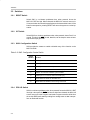
2.2 Default Configuration
Although much of the MSC1211EVM operation is controlled by the host PC,
some configuration must be done directly on the board, using four jumpers
(shorting blocks). The MSC1211EVM is configured at the factory, as shown in
Table 2–1.
Table 2–1. Factory Jumper Settings
Jumper identifier
Description
Default Setting
JMP5
Analog power supply source
1–2
JMP6
Digital power supply source
1–2
J7
Internal Reference Select
1–2
For more information about the jumpers, see section 3.1.
2-2
Quick Start
2.3 Quick Start
Once the MSC1211EVM has been unpacked from its shipping container, and
you have verified that the board is configured as shown in Table 2–1, it can be
powered on and tested.
First, connect the board to the host PC using the supplied 9-pin serial cable. Then,
power the board on by plugging the wall power adapter into a suitable ac power
source and plugging the barrel plug into the barrel jack (J6) on the MSC1211EVM.
(You do not have to connect the serial cable first; it is also acceptable to apply
power to the board first.) When the board is properly powered on, the two green
power-good indicator lamps near the power connectors will glow brightly.
Place the CD-ROM into your CD–ROM drive. Table 2–2 shows the directories
located on the CD-ROM.
Table 2–2. CD-Rom Contents
Directory
Description
8051 Reference
Some reference documentation on the 8051
8051 Tutorial
An HTML tutorial from 8052.com
ADC Demo
A Visual demonstration of the operation of the
MSC1211
Application Notes
Several Application notes for the MSC family
BASIC
BASIC–52 and MDL–BASIC
C Programming
Some information on C–Programming on 8051s
Downloader
Program for loading HEX files into the MSC Flash
memory
EVMS
Design documents for the MSC EVMs
Example Programs
Various example programs for the MSC devices
Hitex ICE
An example of an external ICE which can be used
with the MSC
MSC1210 Data Sheet
MSC1210 User Manual
Ride
Full featured C/Assembly development/simulator environment
Wickenhauser
A low cost C compiler for the MSC1210
Now, install two pieces of software on your PC: RIDE and the Download Tool.
If you are running a Windows platform that is NT-based, such as Windows NT
or Windows 2000, you will need administrator privileges to install the software.
Follow the instructions that the installers give you.
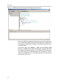
Once the programs has been successfully installed, you can execute them.
When the RIDE development system is run, it displays a splash screen, and
then you will see something like the screen in Figure 2–1.
Getting Started
2-3
Quick Start
Figure 2–1. RIDE (Raisonance Integrated Development Environment)
Refer to the RIDE documentation and help menus for more information about
how to interact with the RIDE environment. When a program is compiled, it can
be immediately downloaded into the MSC1211EVM by using the MSC download utility program.
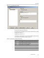
In the Project menu, select Options
Tools, and then Create or Edit
MSC1210_LOADER. Enter the path to the download.exe program that should
be installed in your Windows directory. The download.exe file will need to be
in the current directory or the Windows path. In the “translate from” and the
“translate to” windows add “*.aof”. Select Advanced and you will have see the
screen shown in Figure 2–2.
2-4
Quick Start
Figure 2–2. Tool Advanced Options
UnCheck the Prompt before running box.
All operands should immediately follow the switch character with no spaces
except between options. i.e.:
/F{NODE3}.hex /X22 /P1 /H /T
If the filename, crystal frequency, or port are not included, a screen will prompt
for the values. The operand list is defined in Table 2–3.
Table 2–3. Downloader Operand Definitions
Operand
Definition
/Ffile
hex file, {NODE3} in the RIDE will substitute the hex file (required)
/Xfreq
MSC1211 Xtal Clock frequency (required)
/Pport
PC Comm port 1, 2, 3 or 4 (required)
/Bbaud
Baud rate (standard rates), otherwise it is computed from /Xfreq
/H
If this flag is present the configuration bytes will be erased
/T
This flag requests a terminal window after download.
Getting Started
2-5
Chapter 3
This chapter describes each function of the MSC1211EVM, and how to use the
accompanying software to program and use the MSC1211.
Topic
Page
3.1
Jumpers . . . . . . . . . . . . . . . . . . . . . . . . . . . . . . . . . . . . . . . . . . . . . . . . . . . . . 3-2
3.2
Switches . . . . . . . . . . . . . . . . . . . . . . . . . . . . . . . . . . . . . . . . . . . . . . . . . . . . . 3-4
3.3
I/O Connectors and Signals . . . . . . . . . . . . . . . . . . . . . . . . . . . . . . . . . . . . 3-6
3.4
Circuit Descriptions . . . . . . . . . . . . . . . . . . . . . . . . . . . . . . . . . . . . . . . . . . 3-11
Operation
3-1
Jumpers
3.1 Jumpers
Table 3–1 shows the function of each jumper on the EVM.
Table 3–1. Jumper/Function Reference
Reference
Designator
Setting/Pin
Function
Default
Subsection
JMP1
1 to 2
Short R1 for IDAC0 output
Disconnected
3.1.1
JMP2
1 to 2
Short R2 for IDAC1 output
Disconnected
3.1.2
JMP3
1 to 2
Connect I2C SDA signal
Disconnected
3.1.3
JMP4
1 to 2
Connect I2C SCL signal
Disconnected
3.1.4
JMP5
1 to 2
Onboard AVDD
1–2
3.1.5
2 to 3
External AVDD
1 to 2
Onboard DVDD
1–2
3.1.6
2 to 3
External DVDD
1
AGND
1–2
3.1.7
2
REF IN–
3
VDAC1
4
REF IN+/REFOUT
5
Open
6
AVDD
1
Memory A14
RAM
3.1.8
2
MSC1211 A15
1–3, 2–4, 5–6
3
MSC1211 A14
4
Memory A15
5
Memory /WE
6
MSC1211 /WE
JMP6
J7
J16
3-2
Jumpers
3.1.1
JMP1: Short R1
In order to allow current output IDAC0 to have full compliance, JMP1 can
be used to short out resistor R1, which is in series with that signal.
3.1.2
JMP2: Short R2
In order to allow current output IDAC0 to have full compliance, JMP2 can
be used to short out resistor R2, which is in series with that signal.
3.1.3
JMP3: I2C Data SDA Enable
The MSC1211 uses the same signals for SPI and I2C. Since there is no chip
select available for the I2C device, this jumper will allow the isolation of the
256K EEPROM during SPI testing.
3.1.4
JMP3: I2C Data SCL Enable
The MSC1211 uses the same signals for SPI and I2C. Since there is no chip
select available for the I2C device, this jumper will allow the isolation of the
256K EEPROM during SPI testing.
3.1.5
JMP5: AVDD Power Source Select
The MSC1211 has separate analog and digital power supplies. Use JMP5 to
connect the desired voltage source for the analog power supply AVDD. Shorting pins 1 and 2 connects the onboard 5V regulator. Pins 2–3 can be used to
supply an external voltage for use as AVDD; pin 2 is for the external voltage and
pin 3 is for AGND.
3.1.6
JMP6: DVDD Power Source Select
The MSC1211 has separate analog and digital power supplies. Use JMP6 to
connect the desired voltage source for the digital power supply DVDD. Shorting
pins 1 and 2 connects the onboard 5V regulator. Pins 2–3 can be used to supply an external voltage for use as DVDD; pin 2 is for the external voltage and
pin 3 is for AGND.
3.1.7
J7: Reference Select
J7 has six pins. For normal operation pins 1 and 2 are connected for REF IN–
to be connected to AGND. Since the MSC1210 has a very similar pinout to the
MSC1210, the MSC1211 board is designed to accommodate the MSC1210
device. For the MSC1210, the VDAC1 pin is the REFOUT pin. Therefore, a
connection between pins 3 and 4 will provide the other required connection for
use of the internal reference for the MSC1210. Only pins 1 and 2 are needed
for the MSC1211. Pins 4 and 6 can be connected together, if you want to use
AVDD as the reference voltage.
3.1.8
J16: Memory Configuration
The MSC1211EVM can use either RAM or EEPROM in the socket for U9. The
J16 jumper provides the capability to configure the Addressing and Write Enable signals for each use. For use with compatible EEPROMs, the following pins
are shorted: 1–2, 3–5 and 4–6. For use with the RAM memory that comes standard on the MSC1211EVM, the following pins are shorted: 1–3, 2–4, 5–6.
Operation
3-3
Switches
3.2 Switches
3.2.1
RESET Switch
Switch SW1 is a miniature pushbutton that, when pressed, forces the
MSC1211 RST line high. When released, the MSC1211 enters a reset cycle.
If communication becomes disrupted between the host and the board, or the
board is unresponsive, pressing RESET will return the system to normal operation.
3.2.2
INT Switch
Switch SW2 is a miniature pushbutton that, when pressed, shorts Port 3.2 to
ground. This pin is the INT0 pin and, therefore, can be setup to cause an interrupt when this pin goes low.
3.2.3
SW3: Configuration Switch
SW3 provides the means to enable or disable many of the function on the
MSC1211EVM.
Table 3–2. SW3: Configuration Control Switch
Switch
Number
3.2.4
Function
1
Enables pin P3.5 to control the Yellow LED D5
2
Enables pin P3.4 to control the Red LED D4.
3
Enables pin P3.3 to drive the speaker.
4
Enables pin P3.0 to receive data from Serial0 (J5)
5
Disables on–board 22.1184MHz crystal oscillator
6
Enables pin P1.2 to receive data from Serial1 (J4)
7
Allows DTR from Serial0 to reset MSC1211
8
Allows RTS from Serial0 to reset to Prog Load mode
PRG LD Switch
SW4 is a miniature pushbutton that, when pressed, forces the MSC1211 RST
line high. It also pulls the PSEN line low so that when released, the MCU will
enter a reset cycle in the Program Load mode. Program execution will be from
the on-chip ROM, and it starts by waiting for a carriage return so that it can perform an autobaud function.
3-4
Switches
3.2.5
SW5: Emulation and Control Switch
SW5 provides the means to break several signals so that they can be controlled by an emulator plugged into J14. This switch also provides a means
of setting the operating mode of the MSC1211.
Table 3–3. SW5: Configuration Control Switch
Switch
number
Function
1
Enables the /RD signal or breaks for emulator use.
2
Enables the /WR signal or breaks for emulator use.
3
Enables the Reset signal or breaks for emulator use.
4
Enables the PSEN signal or breaks for emulator use.
5
Provides a method to pull PSEN low.
6
Enables banks switching of 128K RAM memory
7
Provides a method to pull ALE low.
8
Connects EA to DGND
Operation
3-5
I/O Connectors and Signals
3.3 I/O Connectors and Signals
The various connectors on the MSC1211EVM are described in this section.
3.3.1
J8: Serial0 RS-232 Connector
The host PC communicates with the MSC1211EVM through this connector,
which is a D-shell type, 9-pin female, pinned out in the usual manner. Some
of the flow control lines are used for special purposes by the MSC1211EVM
board; these are described in Table 3–4.
In the RS-232 electrical specification, –5V to –15V on a line indicates a logic
high (mark), and +5V to +15V indicates logic low (space). Line states are described here according to their logical states.
If a non-handshaking RS-232 cable is used (i.e., one that connects only RD,
TD, and signal ground), the board can still operate normally, but it cannot be
reset by the host PC, and bootstrap firmware upgrading cannot be performed
through the serial port.
Table 3–4. J8: RS-232 Port Pinout
3-6
Pin
Number
Signal
Name
RS-232
Name
Direction
(at board)
1
DCD
Data Carrier Detect
Output
None
2
RD
Receive Data
Output
Serial data output to the host PC
3
TD
Transmit Data
Input
Serial data input from the host PC
4
DTR
Data Terminal Ready
Input
Connected to the reset circuit.
A low-to-high transition on this line
resets the MCU.
5
SG
Signal Ground
Power
Ground reference
6
DSR
Data Set Ready
Output
None
7
RTS
Request To Send
Input
8
CTS
Clear To Send
Output
None
9
RI
Ring Indicator
Output
None
Function
Connected to PROG LOAD
function. Used to enter serial
programming mode.
A high-to-low transition resets the
MCU and puts it into serial
programming mode.
I/O Connectors and Signals
3.3.2
J9: Serial1 RS-232 Connector
This connector is available for use with the second UART in the MSC1211.
Only the TD and RD lines are used. The DTR pin is connected to the DSR
pin, and the RTS pin is connected to the CTS pin.
In the RS-232 electrical specification, –5V to –15V on a line indicates a logic high (mark), and +5V to +15V indicates logic low (space). Line states are
described here according to their logical states.
Signal descriptions are described in Table 3–5.
Table 3–5. J8: RS-232 Port Pinout
Pin
Number
Signal
Name
RS-232
Name
Direction
(at board)
1
DCD
Data Carrier Detect
Output
None
2
RD
Receive Data
Output
Serial data output to the host PC
3
TD
Transmit Data
Input
Serial data input from the host PC
4
DTR
Data Terminal Ready
Input
Connected to DSR
5
SG
Signal Ground
Power
Ground reference
6
DSR
Data Set Ready
Output
Connected to DTR
7
RTS
Request To Send
Input
Connected to CTS
8
CTS
Clear To Send
Output
Connected to RTS
9
RI
Ring Indicator
Output
None
Function
Operation
3-7
I/O Connectors and Signals
3.3.3
J6, JMP5, JMP6, B1: Power Connectors
The MSC1211EVM features a flexible power supply. Externally generated
power, the onboard regulator circuitry and supplied wall-wart, or a 9V battery
can all be used to supply power. Furthermore, the separated analog and digital
power supplies can be powered differently; e.g., the analog power supply can
be powered externally, and the digital power supply can use the onboard regulator, at the same time; this is configured using jumpers JMP5 and JMP6. The
exception to this is that the battery and wall–wart cannot be used at the same
time (see following paragraph).
Four power connectors are provided: JMP5 (pins 2–3) and JMP6 (pins 2–3)
for external power, battery terminal B1 for a 9V transistor radio battery, and J6
for the supplied wall-wart. J6 is a switched jack—connecting a plug to J6 automatically disconnects the battery terminal. This prevents the battery and J6
from supplying power simultaneously.
Battery power is regulated by the same circuitry that regulates J6 (wall–wart)
power. Note that when a battery is connected to B1, approximately one half
of the prototyping area is covered up by the battery.
Caution: Be very careful when connecting external power supplies
to JMP5 (pins 2 and 3) and JMP6 (pins 2 and 3). They are not
protected against reversed polarity. If you connect them
backwards (i.e., with reversed polarity), it is likely that the
MSC1211EVM will be permanently damaged.
Table 3–6. Unregulated Power Input Connector
Terminal name
Tip
Sleeve
Function
Positive power supply input
Power ground
Table 3–7. B1: 9V Battery Connector
Terminal name
3-8
Function
Split (female) ring
Positive
(mates with solid/male post on battery)
Solid (male) ring
Negative
(mates with split/female post on battery)
I/O Connectors and Signals
3.3.4
J4: Analog Inputs
Terminal block J4 is the main analog input to the MSC1211EVM, as is defined
in Table 3–8. One terminal is provided for each of the nine MSC1211 differential inputs. Each terminal is connected to the MSC1211 through a 1kΩ resistor.
Table 3–8. J4: Analog Inputs
3.3.5
Terminal
Number
Terminal
Name
MSC1211
Pin Number
1
AN0
18
Analog Input 0
2
AN1
19
Analog Input 1
3
AN2
20
Analog Input 2
4
AN3
21
Analog Input 3
5
AN4
22
Analog Input 4
6
AN5
23
Analog Input 5
7
AN6/EXTD
24
Analog Input 6 and
Digital Low Voltage Detect
8
AN7/EXTA
25
Analog Input 7 and
Analog Low Voltage Detect
9
AINCOM
26
Analog Common
10
AGND
17, 27
Function
Analog Ground
J7: External Reference Input
The MSC1211EVM has an onboard 2.5V/1.25V bandgap reference. If a lowernoise reference source or a reference with a different voltage is desired, it can
be connected to square pin connector J7. The reference source (onboard or
external) is selected using pins 1 and 2 of J7. Bypassing for the reference inputs is provided by C17 and C18. To use the internal REFOUT signal, connect
pins 1 and 2 together.
Table 3–9. J7: External Reference Input
Terminal
Number
Function
1
AGND—Analog Ground
2
REF IN–
3
VDAC1/(REF+ for MSC1211)
4
REF IN+/REFOUT
5
Open
6
AVDD
Operation
3-9
I/O Connectors and Signals
3.3.6
TP1–6: Test Points
The test points can be used to monitor certain signals on the board.
For information on the signals connected directly to the MSC1211, consult the
MSC1211 datasheet (SBAS267) located at www.ti.com.
Table 3–10.TP1–6: Test Points
Test Point
Designator
MSC1211
Pin Number
MSC1211
Pin Name
TP1
—
—
TP3
6
P3.3/INT1/PWM
TP4
—
—
RTS on Serial0
TP5
—
—
DTR on Serial0
TP6
—
—
RX on Serial0
TP7
—
—
TX on Serial0
TP8
13
RST
TP9
44
PSEN
TP10
—
—
A0
TP11
—
—
A1
TP12
—
—
A2
TP13
—
—
A3
TP14
—
—
A4
TP15
—
—
A5
TP16
—
—
A6
TP17
—
—
A7
TP18
48
EA
External Memory Enable
TP19
45
ALE
Address Latch Enable
3-10
Signal Description
GND
PWM output connected to the speaker
Reset signal to the MSC1211
Program Select Enable from MSC1211
Circuit Descriptions
3.4 Circuit Descriptions
The MSC1211EVM combines the MSC1211 microcontroller, 128K RAM, the
ADS8325, 256K EEPROM, a 22.1184MHz crystal, support for two serial ports,
and other support circuits to aid in the evaluation of the MSC1211.
3.4.1
MSC1211
The MSC1211 (U5) is clocked by the 22.1184MHz crystal oscillator, unless it
is disabled with switch SW3–6. When the oscillator is disabled, the MSC1211
can use crystal X1 to provide the clock source using on–chip circuitry, although
oscillator X2 must be removed from the board for reliable crystal operation. Inputs come from J4 through current-limiting resistors R1–R9.
Programs can be loaded into the 32K bytes of flash memory using the serial
port (Serial0). The MSC1211 has 1,380 bytes of on–chip RAM. Extra RAM is
available through the use of the 128K RAM (U9). 64K of RAM is directly addressable, with P1.4 providing the means for bank switching.
For detailed information about the MSC1211, consult the MSC1211 product
datasheet (SBAS267) located at www.ti.com.
3.4.2
Programming and Host Communication
The Raisonance integrated software environment (RIDE) and the TI Downloader program make for a convenient system of program development,
download, and execution.
Full source code for the MSC1211EVM firmware is included on the CD-ROM.
3.4.3
Power Supply
Power is brought into the board through external power connectors JMP5
(pins 2 and 3) and JMP6 (pins 2 and 3), battery connector B1, or unregulated
power input J6. If a wall power adaptor is plugged into J6, the battery is disconnected.
Power supplied from the battery or through J6 is regulated by voltage regulators U3, and U4, which provide +5V digital and +5V analog supplies.
Power supplied from the external connectors (JMP5 and JMP6) is not filtered; regulated power of the correct voltages must be supplied to these
connectors.
The board is laid out with separate analog and digital power supplies. Analog power is 5V and is supplied from regulator U3, or external power connector JMP5. 5V digital power is supplied from regulator U4 or JMP6.
When the external power connector J6 is used, it supplies regulator U3 and
U4.
Operation
3-11
Chapter 4
This chapter contains the schematic drawings and PCB layouts for the
MSC1211EVM board.
Topic
Page
4.1
Schematics . . . . . . . . . . . . . . . . . . . . . . . . . . . . . . . . . . . . . . . . . . . . . . . . . . . 4-2
4.2
Component Locations . . . . . . . . . . . . . . . . . . . . . . . . . . . . . . . . . . . . . . . . . 4-4
4.3
Power-Supply CE Certification . . . . . . . . . . . . . . . . . . . . . . . . . . . . . . . . . 4-5
4.4
Bill of Materials . . . . . . . . . . . . . . . . . . . . . . . . . . . . . . . . . . . . . . . . . . . . . . . 4-6
Physical Description
4-1
Schematics
4.1 Schematics
Figure 4–1. Processor Schematic
4-2
Schematics
Figure 4–2. Power and Analog Inputs Schematic
Physical Description
4-3
Component Locations
4.2 Component Locations
Figure 4–3. Printed Circuit Board Layout
4-4
Power-Supply CE Certification
4.3 Power-Supply CE Certification
Physical Description
4-5
Table 4–1. Bill of Materials
Item No.
Quantity
Value
Designator
Description
Vendor
Part Number
1
13
100Ω
R1–R11, R32, R33
1/10W 5% chip resistor
Panasonic
ERJ–6GEYJ101V
2
4
390Ω
R14–R17
1/16W 5% chip resistor
Panasonic
ERJ–3GEYJ391V
3
2
1kΩ
R19, R27
1/16W 5% chip resistor
Panasonic
ERJ–3GEYJ102V
4
2
2kΩ
R12, R13
1/16W 5% chip resistor
Panasonic
ERJ–3GEYJ202V
5
2
10kΩ
R18, R22
1/16W 5% chip resistor
Panasonic
ERJ–3GEYJ103V
6
8
100kΩ
R23–R26,
R28–R31
1/16W 5% chip resistor
Panasonic
ERJ–3GEYJ104
Not installed
2
7
2
18pF
C9, C14
50V ceramic chip capacitor, ±5%, NPO
Panasonic
ECJ–1VC1H180J
8
1
10000pF
C10
16V ceramic chip capacitor, ±10%, X7R
Panasonic
ECJ–1VB1C103K
9
19
0.1µF
C1, C3, C11,
C15–C21, C23,
C25–C32
16V ceramic chip capacitor, ±10%, X7R
Panasonic
ECJ–1VB1C104K
10
3
0.33µF
C5, C6, C13
16V ceramic chip capacitor, ±10%, X7R
Panasonic
ECJ–2YB1C334K
11
3
0.47µF
C12, C22, C24
16V ceramic chip capacitor, ±10%, X7R
Panasonic
ECJ–2YB1C474K
12
2
1µF
C2, C4
6.3V ceramic chip capacitor, ±10%, X5R
Panasonic
ECJ–1VB0J105K
13
2
10µF
C7, C8
6.3V ceramic chip capacitor, ±10%, X5R
Panasonic
ECJ–3YB0J106K
14
1
D1
Diode 1A 50V SMD MELF
Micro Commercial
Components
DL4001
15
2
D2, D3
LED green clear lens 1206 SMD
Lumex
SML–LX1206GC–TR
16
1
D4
LED red clear lens 1206 SMD
Lumex
SML–LX1206IC–TR
17
1
D5
LED yellow clear lens 1206 SMD
Lumex
SML–LX1205YC–TR
18
1
D6
Diode fast switching SMD miniMELF
Diodes Incorporated
LL4148
(continued on next page)
R20, R21
Bill of Materials
4-6
4.4 Bill of Materials
Table 4–1. Bill of Materials (continued)
Item No.
Quantity
19
Description
Vendor
Part Number
1
SP1
Piezoelectric ceramic buzzer
Panasonic
EFB–AA14D001
20
1
X1
22.1184MHz quartz crystal thru-hole
Citizen
HC49US22.11840592MABJ
Not installed
1
X2
5V 22.1184MHz programmable oscillator SMD
Epson
SG–8002CA–22.1184M–PHB
21
1
U1
16-bit SAR analog-to-digital converter (ADC)
Texas Instruments
ADS8325IBDGKT
22
1
U2
256K I2C CMOS serial EEPROM
MicroChip
24LC256I/SN
23
2
U3, U4
+5V 1A low-dropout voltage regulator
Texas Instruments
REG1117FA–5.0
24
1
U5
24-bit 8-channel intelligent ADC
Texas Instruments
MSC1211
25
1
U6
Multi-channel RS-232 line driver/receiver
Texas Instruments
MAX3243CPWR
26
2
U7, U8
Single IC buffer driver with open drain o/p
Texas Instruments
SN74LVC1G07DBVR
27
1
U9
128K x 8-bit CMOS SRAM
Brilliance
Semiconductor
BS62LV1024PI–70
28
1
U10
Octal D-type latches with 3-state outputs
Texas Instruments
SN74HC573APWR
29
1
U11
Supervisory circuit active high reset
Texas Instruments
TPS3837L30DBVT
30
1
U12
Supervisory circuit active low open drain
Texas Instruments
TPS3838L30DBVT
31
1
U13
Triple 3-input NAND gates
Texas Instruments
SN74AC10PWR
32
1
U14
Single 2-input NAND gate
Texas Instruments
SN74AHC1G08DBVR
33
1
U15
Single 2-input positive NOR gate
Texas Instruments
SN74AHC1G02DBVR
34
1
U16
3-line to 8-line decoder/demultiplexer
Texas Instruments
SN74AHC138PWR
35
1
N/A
MSC1211EVM PWB
Texas Instruments
6443406
36
1
B1 (+)
9V battery clip female
Keystone Electronics
594
37
1
B1 (–)
9V battery clip male
Keystone Electronics
593
38
2
J8, J9
DB9 right angle female conn. w/board locks
Tyco/AMP
747844–4
39
1
J6
2.5mm power connector
CUI Stack
PJ–102B
4-7
Bill of Materials
Physical Description
Designator
(continued on next page)
Value
Item No.
Quantity
Not installed
Value
Designator
Description
Vendor
Part Number
2
J14
1 x 15 single row socket .050′′ spacing
Mill-Max
851–93–050–10–001 (15)
Not installed
1
J15
1 x 8 header, 0.1′′ spacing
Samtec
TSW–108–07–L–D
40
3
J5, J10, J11
2 contact screw terminal block, 3.5mm
On Shore Technology
ED555/2DS
41
1
J4
10 contact screw terminal block, 3.5mm
On Shore Technology
ED555/10DS
Not installed
1
J13
2 x 3 header, 0.1′′ spacing
Samtec
TSW–103–07–L–D
42
2
J7, J16
2 x 3 header, 0.1′′ spacing
Samtec
TSW–103–07–L–D
Not installed
1
J12
2 x 4 header, 0.1′′ spacing
Samtec
TSW–104–07–L–D
Not installed
4
J0, J1, J2, J3
2 x 5 header, 0.1′′ spacing
Samtec
TSW–105–07–L–D
43
4
JMP1–JMP4
2-position jumper, 0.1′′ spacing
Samtec
TSW–102–07–L–S
44
2
JMP5, JMP6
3-position jumper, 0.1′′ spacing
Samtec
TSW–103–07–L–S
45
3
SW1, SW2, SW4
Momentary pushbutton tact switch
Omron
B3F–1002
46
2
SW3, SW5
8-pos DIP switch, half pitch SMD
C&K Components, Inc.
TDA08H0SK1
47
1
TP1
Large loop test point switch
Keystone Electronics
5011
48
18
TP2–TP19
Miniature test point terminal
Keystone Electronics
5000
49
6
R20, R21, X1
Miniature spring socket
Tyco/AMP
50863–5
50
11
N/A
Shorting jumper
Samtec
SNT–100–BK–TH
51
4
N/A
1/4′′ x .625 hex 4-40 threaded standoff
Keystone Electronics
1808
52
4
N/A
Pan head machine screws 4-40 x 1/2′′ phillips
Building Fasteners
PMS 440 0050 PH
53
1
U9
32-pin low profile, open frame DIP socket
Mill-Max
115–93–632–41–003
Bill of Materials
4-8
Table 4–1. Bill of Materials (continued)