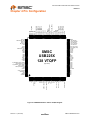
1
USB2250/50i/51/51i
Ultra Fast USB 2.0 Multi-Slot
Flash Media Controller
Datasheet
PRODUCT FEATURES
General Description
The SMSC USB2250/50i/51/51i is a USB 2.0 compliant, high
speed Mass Storage Class Peripheral Controller intended for
reading and writing to more than 24 popular flash media
formats from the CompactFlash® (CF), SmartMediaTM (SM), xD
Picture CardTM (xD)1, Memory StickTM (MS), Secure Digital
(SD), and MultiMediaCardTM (MMC) families.
The SMSC USB2250/50i/51/51i is a fully integrated, single
chip solution capable of ultra high performance operation.
Average sustained transfer rates exceeding 35MB/s are
possible if the media and host can support those rates.
General Features
128-pin VTQFP (14x14mm) lead-free RoHS compliant
Targeted for applications in which single or "combo" media
sockets are used
Supports multiple simultaneous card insertions
Flexible assignment of number of LUNs and how card types
are associated with the LUNs
package
Hardware-controlled data flow architecture for all selfmapped media
Pipelined hardware support for access to non-selfmapped media
Product name with “i” denotes the version that supports
the industrial temperature range of -40ºC to 85ºC
Hardware Features
Single Chip Flash Media Controller with non-multiplexed
interface for independent card sockets
Flash Media Specification Revision Compliance
— Compact Flash Specification 4.1
–
–
CF UDMA Modes 0-4
CF PIO Modes 0-6
OEM Selectable Features
VID/PID/Language ID
28-character Manufacturer ID and Product string
12-hex digit (max) Serial Number string
Customizable Vendor specific data by optional use of
external serial EEPROM
Bus- or Self-powered selection
LED blink interval or duration
Internal power FET configuration
Software Features
— Memory Stick Specification 1.43
— Memory Stick Pro Format Specification 1.02
— Memory Stick Pro-HG Duo Format Specification 1.01
–
Memory Stick, MS Duo, HS-MS, MS Pro-HG, MS Pro
— xD Picture Card 1.2
— Smart Media Specification 1.3
— Secure Digital 2.0
–
— MultiMediaCard Specification 4.2
–
HS-SD, HC-SD, TransFlash™ and reduced form factor
media
1/4/8 bit MMC
SDIO and MMC Streaming Mode support
Extended configuration options
— xD player mode operation
— Socket switch polarities, etc.
Media Activity LED
GPIO configuration and polarity
— Up to 11 GPIOs (based on configuration) for special
function use: LED indicators, button inputs, power
control to memory devices, etc. The number of actual
GPIO’s depends on the implementation configuration
used.
— Four GPIO’s with up to 200 mA drive
— An additional 16 GPIO’s if CF is not used
On Board 24MHz Crystal Driver Circuit
Optional external 24MHz clock input
4 Independent Internal Card Power FET
— 200mA each
— "Fold-back" short circuit current protected
8051 8-bit microprocessor
— 60MHz - single cycle execution
— 64KB ROM; 14KB RAM
Internal Regulator for 1.8V core operation
Optimized pinout improves signal routing, easing
implementation and allowing for improved signal integrity
Optimized for low latency interrupt handling
Reduced memory footprint
Device Firmware Upgrade (DFU) support of external
EEPROM or External Flash
— Assembly line support
— End user field upgrade support
— DFU Package consists of driver, firmware, sample DFU
application and source code, DFU driver API
Optional custom firmware with external ROM (up to 128k)
Please see the USB2250/50i/51/51i Software Release
Notes for additional Software Features.
Applications
Flash Media Card Reader/Writer
Printers
Desktop and Mobile PCs
Consumer A/V
Media Players/Viewers
Vista ReadyBoostTM
1.) xD Picture Card not applicable to USB2251.
SMSC USB2250/50i/51/51i
DATASHEET
Revision 1.1 (05-29-08)
Ultra Fast USB 2.0 Multi-Slot Flash Media Controller
Datasheet
ORDER NUMBER:
USB2250/50i/51/51i-NU-XX for 128-pin, VTQFP Lead-Free RoHS Compliant Package
“XX” in the order number indicates the internal ROM firmware revision level.
Please contact your SMSC sales representative for more information.
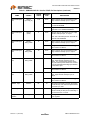
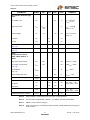
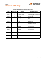
Table 0.1 USB2250/50i/51/51iComparison of Features
CompactFlash®
Memory StickTM
Secure Digital
MultiMediaCardTM
SmartMediaTM
xD Picture
CardTM
Operational
temperature
USB2250
.
.
0ºC to 70ºC
USB2250i
.
.
-40ºC to 85ºC
USB2251
.
0ºC to 70ºC
USB2251i
.
-40ºC to 85ºC
Part Number
80 ARKAY DRIVE, HAUPPAUGE, NY 11788 (631) 435-6000, FAX (631) 273-3123
Copyright © 2008 SMSC or its subsidiaries. All rights reserved.
Circuit diagrams and other information relating to SMSC products are included as a means of illustrating typical applications. Consequently, complete
information sufficient for construction purposes is not necessarily given. Although the information has been checked and is believed to be accurate, no
responsibility is assumed for inaccuracies. SMSC reserves the right to make changes to specifications and product descriptions at any time without notice.
Contact your local SMSC sales office to obtain the latest specifications before placing your product order. The provision of this information does not convey
to the purchaser of the described semiconductor devices any licenses under any patent rights or other intellectual property rights of SMSC or others. All sales
are expressly conditional on your agreement to the terms and conditions of the most recently dated version of SMSC's standard Terms of Sale Agreement
dated before the date of your order (the "Terms of Sale Agreement"). The product may contain design defects or errors known as anomalies which may cause
the product's functions to deviate from published specifications. Anomaly sheets are available upon request. SMSC products are not designed, intended,
authorized or warranted for use in any life support or other application where product failure could cause or contribute to personal injury or severe property
damage. Any and all such uses without prior written approval of an Officer of SMSC and further testing and/or modification will be fully at the risk of the
customer. Copies of this document or other SMSC literature, as well as the Terms of Sale Agreement, may be obtained by visiting SMSC’s website at
http://www.smsc.com. SMSC is a registered trademark of Standard Microsystems Corporation (“SMSC”). Product names and company names are the
trademarks of their respective holders.
SMSC DISCLAIMS AND EXCLUDES ANY AND ALL WARRANTIES, INCLUDING WITHOUT LIMITATION ANY AND ALL IMPLIED WARRANTIES OF
MERCHANTABILITY, FITNESS FOR A PARTICULAR PURPOSE, TITLE, AND AGAINST INFRINGEMENT AND THE LIKE, AND ANY AND ALL WARRANTIES
ARISING FROM ANY COURSE OF DEALING OR USAGE OF TRADE. IN NO EVENT SHALL SMSC BE LIABLE FOR ANY DIRECT, INCIDENTAL, INDIRECT,
SPECIAL, PUNITIVE, OR CONSEQUENTIAL DAMAGES; OR FOR LOST DATA, PROFITS, SAVINGS OR REVENUES OF ANY KIND; REGARDLESS OF THE FORM
OF ACTION, WHETHER BASED ON CONTRACT; TORT; NEGLIGENCE OF SMSC OR OTHERS; STRICT LIABILITY; BREACH OF WARRANTY; OR OTHERWISE;
WHETHER OR NOT ANY REMEDY OF BUYER IS HELD TO HAVE FAILED OF ITS ESSENTIAL PURPOSE, AND WHETHER OR NOT SMSC HAS BEEN ADVISED
OF THE POSSIBILITY OF SUCH DAMAGES.
SMSC USB2250/50i/51/51i
2
DATASHEET
Revision 1.1 (05-29-08)
Ultra Fast USB 2.0 Multi-Slot Flash Media Controller
Datasheet
Table of Contents
Chapter 1 Acronyms . . . . . . . . . . . . . . . . . . . . . . . . . . . . . . . . . . . . . . . . . . . . . . . . . . . . . . . . . 6
Chapter 2 Block Diagram . . . . . . . . . . . . . . . . . . . . . . . . . . . . . . . . . . . . . . . . . . . . . . . . . . . . . 7
Chapter 3 Pin Table . . . . . . . . . . . . . . . . . . . . . . . . . . . . . . . . . . . . . . . . . . . . . . . . . . . . . . . . . . 8
3.1
128-Pin Package . . . . . . . . . . . . . . . . . . . . . . . . . . . . . . . . . . . . . . . . . . . . . . . . . . . . . . . . . . . . . . . 8
Chapter 4 Pin Configuration . . . . . . . . . . . . . . . . . . . . . . . . . . . . . . . . . . . . . . . . . . . . . . . . . 10
Chapter 5 Pin Descriptions . . . . . . . . . . . . . . . . . . . . . . . . . . . . . . . . . . . . . . . . . . . . . . . . . . . 11
5.1
5.2
USB2250/50i/51/51i 128-Pin VTQFP Pin Descriptions . . . . . . . . . . . . . . . . . . . . . . . . . . . . . . . . . 11
Buffer Type Descriptions . . . . . . . . . . . . . . . . . . . . . . . . . . . . . . . . . . . . . . . . . . . . . . . . . . . . . . . . 20
Chapter 6 Pin Reset State Table . . . . . . . . . . . . . . . . . . . . . . . . . . . . . . . . . . . . . . . . . . . . . . . 21
6.1
128-Pin Reset States . . . . . . . . . . . . . . . . . . . . . . . . . . . . . . . . . . . . . . . . . . . . . . . . . . . . . . . . . . . 22
Chapter 7 DC Parameters . . . . . . . . . . . . . . . . . . . . . . . . . . . . . . . . . . . . . . . . . . . . . . . . . . . . 28
7.1
7.2
7.3
7.4
Maximum Guaranteed Ratings . . . . . . . . . . . . . . . . . . . . . . . . . . . . . . . . . . . . . . . . . . . . . . . . . . . .
Recommended Operating Conditions. . . . . . . . . . . . . . . . . . . . . . . . . . . . . . . . . . . . . . . . . . . . . . .
DC Electrical Characteristics . . . . . . . . . . . . . . . . . . . . . . . . . . . . . . . . . . . . . . . . . . . . . . . . . . . . .
Capacitance . . . . . . . . . . . . . . . . . . . . . . . . . . . . . . . . . . . . . . . . . . . . . . . . . . . . . . . . . . . . . . . . . .
28
29
30
32
Chapter 8 AC Specifications . . . . . . . . . . . . . . . . . . . . . . . . . . . . . . . . . . . . . . . . . . . . . . . . . . 33
8.1
Oscillator/Clock. . . . . . . . . . . . . . . . . . . . . . . . . . . . . . . . . . . . . . . . . . . . . . . . . . . . . . . . . . . . . . . . 33
Chapter 9 Package Outline . . . . . . . . . . . . . . . . . . . . . . . . . . . . . . . . . . . . . . . . . . . . . . . . . . . 34
Chapter 10 GPIO Usage . . . . . . . . . . . . . . . . . . . . . . . . . . . . . . . . . . . . . . . . . . . . . . . . . . . . . . 35
SMSC USB2250/50i/51/51i
3
DATASHEET
Revision 1.1 (05-29-08)
Ultra Fast USB 2.0 Multi-Slot Flash Media Controller
Datasheet
List of Figures
Figure 2.1
Figure 4.1
Figure 6.1
Figure 6.2
Figure 6.3
Figure 7.1
Figure 8.1
Figure 8.2
Figure 9.1
USB2250/50i/51/51i Block Diagram. . . . . . . . . . . . . . . . . . . . . . . . . . . . . . . . . . . . . . . . . . . . . 7
USB2250/50i/51/51i 128-Pin VTQFP Diagram . . . . . . . . . . . . . . . . . . . . . . . . . . . . . . . . . . . 10
Pin Reset States . . . . . . . . . . . . . . . . . . . . . . . . . . . . . . . . . . . . . . . . . . . . . . . . . . . . . . . . . . 21
Legend for Pin Reset States Table . . . . . . . . . . . . . . . . . . . . . . . . . . . . . . . . . . . . . . . . . . . . 21
USB2250/50i/51/51i Pin Reset States . . . . . . . . . . . . . . . . . . . . . . . . . . . . . . . . . . . . . . . . . . 22
Supply Rise Time Model . . . . . . . . . . . . . . . . . . . . . . . . . . . . . . . . . . . . . . . . . . . . . . . . . . . . 29
Typical Crystal Circuit . . . . . . . . . . . . . . . . . . . . . . . . . . . . . . . . . . . . . . . . . . . . . . . . . . . . . . 33
Formula to Find Value of C1 and C2 . . . . . . . . . . . . . . . . . . . . . . . . . . . . . . . . . . . . . . . . . . . 33
USB2250/50i/51/51i 128-Pin VTQFP, 14x14x1.0mm Body, 2.0mm Pitch . . . . . . . . . . . . . . . 34
Revision 1.1 (05-29-08)
4
DATASHEET
SMSC USB2250/50i/51/51i
Ultra Fast USB 2.0 Multi-Slot Flash Media Controller
Datasheet
List of Tables
Table 0.1 USB2250/50i/51/51iComparison of Features . . . . . . . . . . . . . . . . . . . . . . . . . . . . . . . . . . . . . . 2
Table 3.1 USB2250/50i/51/51i 128-Pin VTQFP Package . . . . . . . . . . . . . . . . . . . . . . . . . . . . . . . . . . . . . 8
Table 5.2 USB2250/50i/51/51i Buffer Type Descriptions . . . . . . . . . . . . . . . . . . . . . . . . . . . . . . . . . . . . 20
Table 7.1 Pin Capacitance. . . . . . . . . . . . . . . . . . . . . . . . . . . . . . . . . . . . . . . . . . . . . . . . . . . . . . . . . . . . 32
Table 10.1 USB2250/50i/51/51i GPIO Usage (ROM Rev 0x00) . . . . . . . . . . . . . . . . . . . . . . . . . . . . . . . . 35
SMSC USB2250/50i/51/51i
5
DATASHEET
Revision 1.1 (05-29-08)
Ultra Fast USB 2.0 Multi-Slot Flash Media Controller
Datasheet
Chapter 1 Acronyms
CF: Compact Flash
CFC: Compact Flash Controller
EEPROM: Electrically Erasable Programmable Read-Only Memory
FET: Field Effect Transistor
LUN: Logical Unit Number
MMC: MultiMediaCard
MS: Memory Stick
MSC: Memory Stick Controller
PLL: Phase-Locked Loop
RoHS: Restriction of Hazardous Substances Directive
SD: Secure Digital
SDIO: Secure Digital Input/Output
SDC: Secure Digital Controllerl
SIE: Serial Interface Engine
SM: SmartMedia
SMC: SmartMedia Controller
VTQFP: Very Thin Quad Flat Package
xD: xD Picture Card
*Note: In order to develop, make, use, or sell readers and/or other products using or incorporating any of the SMSC devices made
the subject of this document or to use related SMSC software programs, technical information and licenses under patent and other
intellectual property rights from or through various persons or entities, including without limitation media standard companies,
forums, and associations, and other patent holders may be required. These media standard companies, forums, and associations
include without limitation the following: Sony Corporation (Memory Stick, Memory Stick Pro); SD3 LLC (Secure Digital); MultiMedia
Card Association (MultiMediaCard); the SSFDC Forum (SmartMedia); the Compact Flash Association (Compact Flash); and Fuji
Photo Film Co., Ltd., Olympus Optical Co., Ltd., and Toshiba Corporation (xD-Picture Card). SMSC does not make such licenses
or technical information available; does not promise or represent that any such licenses or technical information will actually be
obtainable from or through the various persons or entities (including the media standard companies, forums, and associations), or
with respect to the terms under which they may be made available; and is not responsible for the accuracy or sufficiency of, or
otherwise with respect to, any such technical information.
SMSC's obligations (if any) under the Terms of Sale Agreement, or any other agreement with any customer, or otherwise, with
respect to infringement, including without limitation any obligations to defend or settle claims, to reimburse for costs, or to pay
damages, shall not apply to any of the devices made the subject of this document or any software programs related to any of such
devices, or to any combinations involving any of them, with respect to infringement or claimed infringement of any existing or future
patents related to solid state disk or other flash memory technology or applications ("Solid State Disk Patents"). By making any
purchase of any of the devices made the subject of this document, the customer represents, warrants, and agrees that it has
obtained all necessary licenses under then-existing Solid State Disk Patents for the manufacture, use and sale of solid state disk
and other flash memory products and that the customer will timely obtain at no cost or expense to SMSC all necessary licenses
under Solid State Disk Patents; that the manufacture and testing by or for SMSC of the units of any of the devices made the subject
of this document which may be sold to the customer, and any sale by SMSC of such units to the customer, are valid exercises of
the customer's rights and licenses under such Solid State Disk Patents; that SMSC shall have no obligation for royalties or otherwise
under any Solid State Disk Patents by reason of any such manufacture, use, or sale of such units; and that SMSC shall have no
obligation for any costs or expenses related to the customer's obtaining or having obtained rights or licenses under any Solid State
Disk Patents.
SMSC MAKES NO WARRANTIES, EXPRESS, IMPLIED, OR STATUTORY, IN REGARD TO INFRINGEMENT OR OTHER
VIOLATION OF INTELLECTUAL PROPERTY RIGHTS. SMSC DISCLAIMS AND EXCLUDES ANY AND ALL WARRANTIES
AGAINST INFRINGEMENT AND THE LIKE.
No license is granted by SMSC expressly, by implication, by estoppel or otherwise, under any patent, trademark, copyright, mask
work right, trade secret, or other intellectual property right.
**To obtain this software program the appropriate SMSC Software License Agreement must be executed and in effect. Forms of
these Software License Agreements may be obtained by contacting SMSC.
Revision 1.1 (05-29-08)
6
DATASHEET
SMSC USB2250/50i/51/51i
Ultra Fast USB 2.0 Multi-Slot Flash Media Controller
Datasheet
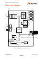
Chapter 2 Block Diagram
SD/
MMC
AUTO_
CBW
PROC
CF/
GPIO (16)
USB
Host
SIE
CTL
PHY
BUS
INTFC
BUS
INTFC
FMDU
CTL
FMI
MS
SM
EP0 TX
EP0 RX
BUS
INTFC
RAM
4K
total
1.8V Reg
EP1 RX
EP1 TX
EP2 RX
EP2 TX
PLL
XDATA BRIDGE
+ BUS ARBITER
PWR_FET0
GPIO9/CARD_PWR1
PWR_FET2
GPIO10/CARD_PWR2
PWR_FET3
GPIO11/CARD_PWR3
GPIOs
RAM
10KB
ROM
64KB*
ADDR
MAP
GPIO8/CARD_PWR0
PWR_FET1
11 pins
Program Memory I/O Bus
Clock
Generation and
Control
SFR
RAM
8051
PROCESSOR
*ROM is not available in USB2259
Figure 2.1 USB2250/50i/51/51i Block Diagram
SMSC USB2250/50i/51/51i
7
DATASHEET
Revision 1.1 (05-29-08)
Ultra Fast USB 2.0 Multi-Slot Flash Media Controller
Datasheet
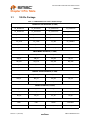
Chapter 3 Pin Table
3.1
128-Pin Package
Table 3.1 USB2250/50i/51/51i 128-Pin VTQFP Package
COMPACTFLASH INTERFACE (28 PINS)
CF_D0/GPIO16
CF_D1/GPIO17
CF_D2/GPIO18
CF_D3/GPIO19
CF_D4/GPIO20
CF_D5/GPIO21
CF_D6/GPIO22
CF_D7/GPIO23
CF_D8/GPIO24
CF_D9/GPIO25
CF_D10/GPIO26
CF_D11/GPIO27
CF_D12/GPIO28
CF_D13/GPIO29
CF_D14/GPIO30
CF_D15/GPIO31
CF_nIOR
CF_nIOW
CF_IRQ
CF_nRESET
CF_IORDY
CF_nCS0
CF_DMACK/TXD/GPIO7
CF_SA0
CF_SA1
CF_SA2
GPIO13 (CF_nCD)
CF_DMARQ/RXD/GPIO2
SMARTMEDIA INTERFACE (17 PINS)
SM_D0
SM_D1
SM_D2
SM_D3
SM_D4
SM_D5
SM_D6
SM_D7
SM_ALE
SM_CLE
SM_nRE
SM_nWE
SM_nWP
SM_nB/R
SM_nCE
GPIO14 (SM_nCD)
SM_nWPS
MEMORY STICK INTERFACE (11 PINS)
MS_BS
MS_D0/MS_SDIO
MS_SCLK
GPIO12 (MS_INS)
MS_D1
MS_D2
MS_D3
MS_D4
MS_D5
MS_D6
MS_D7
SD/MMC INTERFACE (12 PINS)
SD_CMD
SD_CLK
SD_D0
SD_D1
SD_D2
SD_D3
GPIO6 (SD_WP)
GPIO15 (SD_nCD)
SD_D4
SD_D5
SD_D6
SD_D7
USB INTERFACE (8 PINS)
USB+
USB-
RBIAS
VDD18PLL
VDDA33
XTAL2
XTAL1 (CLKIN)
REG_EN
Revision 1.1 (05-29-08)
8
DATASHEET
SMSC USB2250/50i/51/51i
Ultra Fast USB 2.0 Multi-Slot Flash Media Controller
Datasheet
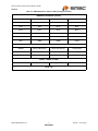
Table 3.1 USB2250/50i/51/51i 128-Pin VTQFP Package (continued)
MEMORY/IO INTERFACE (28 PINS)
MA0/CLK_SEL0
MA1/CLK_SEL1
MA2
MA3
MA4
MA5
MA6
MA7
MA8
MA9
MA10
MA11
MA12
MA13
MA14
MA15
MA16
MD0
MD1
MD2
MD3
MD4
MD5
MD6
MD7
nMRD
nMWR
nMCE
MISC (10 PINS)
nRESET
GPIO3 (VBUS_DET)
GPIO4 (SCL/xD_ID)
GPIO5 (SDA)
LED1 / GPIO1
GPIO8/CARD_PWR0
GPIO9/CARD_PWR1
GPIO10/CARD_PWR2
GPIO11/CARD_PWR3
TEST
DIGITAL, POWER (14 PINS)
(5) VDD33
(1) VDD18
(8) VSS
TOTAL 128
SMSC USB2250/50i/51/51i
9
DATASHEET
Revision 1.1 (05-29-08)
Ultra Fast USB 2.0 Multi-Slot Flash Media Controller
Datasheet
65
66
67
68
69
70
71
72
73
74
75
76
77
78
79
80
81
82
83
84
85
86
87
88
89
90
91
92
93
94
97
64
98
63
99
62
100
61
101
60
102
59
103
58
104
57
105
56
106
55
107
108
109
110
111
112
113
114
115
116
117
SMSC
USB225X
128 VTQFP
54
(Top View)
43
118
119
53
52
51
50
49
48
47
46
45
44
42
32
31
30
29
28
27
26
25
24
23
22
21
20
19
18
17
16
15
14
13
12
nRESET
CF_D5 / GPIO21
CF_D12 / GPIO28
CF_D4 / GPIO20
CF_D11 / GPIO27
CF_D3 / GPIO19
GPIO13 (CF_nCD)
GPIO14 (SM_nCD)
SM_nB/R
SM_nRE
SM_nCE
SM_CLE
SM_ALE
VSS
VDD33
VDD18
SM_nWE
SM_nWP
SM_D0
SM_D1
SM_D2
SM_D3
SM_D4
SM_D5
SM_D6
SM_D7
SM_nWPS
MD0
MD1
MD2
MD3
MD7
MA12
MA15
nMWR
MA14
GPIO5 (SDA)
REG_EN
USB+
USBVSS
SD_D1
SD_D6
SD_D0
SD_D7
GPIO8 / CRD_PWR0
VDD33
GPIO11 / CRD_PWR3
VSS
SD_CLK
SD_D5
SD_CMD
SD_D4
SD_D3
SD_D2
MA10
MA1 / CLK_SEL1
nMCE
MA0 / CLK_SEL0
MA16
MD6
MD5
MD4
GPIO15 (SD_nCD)
11
33
10
34
128
9
35
127
8
36
126
7
37
125
6
38
124
5
39
123
4
40
122
3
41
121
2
120
1
MS_D6
GPIO12 (MS_INS)
MS_D3
MS_D7
MS_SCLK
VSS
TEST
VDD33
GPIO6 (SD_WP)
MA7
MA13
MA6
MA8
MA5
MA9
MA4
MA11
MA3
nMRD
MA2
CF_DMARQ / RXD / GPIO2
GPIO4 (SCL/xD_ID)
CF_DMACK / TXD / GPIO7
LED1 / GPIO1
GPIO3 (VBUS_DET)
VSS
XTAL2
XTAL1 (CLKIN)
VDD18PLL
VSS
RBIAS
VDDA33
95
96
MS_D2
MS_D4
MS_D0 / MS_SDIO
MS_D5
MS_D1
MS_BS
CF_D10 / GPIO26
CF_D9 / GPIO25
CF_D2 / GPIO18
CF_D8 / GPIO24
CF_D1 / GPIO17
CF_D0 / GPIO16
CF_SA0
CF_SA1
CF_SA2
VSS
CF_IORDY
CF_nRESET
GPIO9 / CRD_PWR1
VDD33
GPIO10 / CRD_PWR2
VSS
CF_IRQ
CF_nIOW
CF_nIOR
CF_nCS0
CF_D15 / GPIO31
CF_D7 / GPIO23
CF_D14 / GPIO30
CF_D6 / GPIO22
CF_D13 / GPIO29
VDD33
Chapter 4 Pin Configuration
Figure 4.1 USB2250/50i/51/51i 128-Pin VTQFP Diagram
Revision 1.1 (05-29-08)
10
DATASHEET
SMSC USB2250/50i/51/51i
Ultra Fast USB 2.0 Multi-Slot Flash Media Controller
Datasheet
Chapter 5 Pin Descriptions
This section provides a detailed description of each signal. The signals are arranged in functional
groups according to their associated interface.
The “n” symbol in the signal name indicates that the active, or asserted, state occurs when the signal
is at a low voltage level. When “n” is not present before the signal name, the signal is asserted at the
high voltage level.
The terms assertion and negation are used exclusively. This is done to avoid confusion when working
with a mixture of “active low” and “active high” signals. The term assert, or assertion, indicates that a
signal is active, independent of whether that level is represented by a high or low voltage. The term
negate, or negation, indicates that a signal is inactive.
5.1
USB2250/50i/51/51i 128-Pin VTQFP Pin Descriptions
Table 5.1 USB2250/50i/51/51i 128-Pin VTQFP Pin Descriptions
NAME
SYMBOL
128-PIN
VTQFP
BUFFER
TYPE
DESCRIPTION
COMPACT FLASH INTERFACE
CF Chip Select 0
CF_nCS0
71
O12
This pin is the active low chip select 0 signal
for the task file registers of the CF ATA
device in True IDE mode.
CF Register
Address
CF_SA[2:0]
82
83
84
I/O12
These pins are the register select address
bits for the CF ATA device.
CF Interrupt
CF_IRQ
74
IPD
This is the active high interrupt request
signal from the CF device.
This pin has an internal weak pull-down
resistor that can be controlled by:
CF_INTF_EN bit of CFC_ATA_MODE_CTL.
CF Data 15-8 /
GPIO
CF_D[15:8] /
GPIO[31:24]
70
68
66
62
60
90
89
87
I/O12PD
In True IDE Mode, all task file register
operations occur on the CF_D[7:0], while
data transfer occurs on CF_D[15:0].
The bi-directional data signal has an internal
weak pull-down resistor.
I/O12
SMSC USB2250/50i/51/51i
CF_D[15:8]: The bi-directional data signals
CF_D15 - CF_D8 in True IDE mode data
transfer
11
DATASHEET
GPIO[31:24]: These pins are GPIOs if the
CF_INTF_EN bit of the CFC_ATA_MODE
CTL is disabled and the EXTENDED_GPIO
bit is set in UTIL_CONFIG1 is enabled.
Revision 1.1 (05-29-08)
Ultra Fast USB 2.0 Multi-Slot Flash Media Controller
Datasheet
Table 5.1 USB2250/50i/51/51i 128-Pin VTQFP Pin Descriptions (continued)
NAME
CF Data 7-0 /
GPIO
SYMBOL
CF_D[7:0] /
GPIO[23:16]
128-PIN
VTQFP
BUFFER
TYPE
69
67
63
61
59
88
86
85
I/O12PD
CF_IORDY
CF_D[7:0]: The bi-directional data signals
CF_D7 - CF_D0 in True IDE mode data
transfer. In True IDE Mode, all of the task file
register operations occur on the CF_D[7:0],
while data transfer occurs on CF_D[15:0].
The bi-directional data signal has an internal
weak pull-down resistor.
I/O12
IO Ready
DESCRIPTION
80
IPU
GPIO[23:16]: These Pins are GPIOs if the
CF_INTF_EN bit of the CFC_ATA_MODE
CTL is disabled and the EXTENDED_GPIO
bit set in UTIL_CONFIG1 is enabled.
This pin is the active high input signal for
IORDY.
This pin has an internal weak pull-up resistor
that can be controlled by:
CF_INTF_EN bit of CFC_ATA_MODE CTL.
CF Card
Detection1
GPIO13
(CF_nCD)
58
I/O12
This is a GPIO designated as the Compact
Flash card detection pin.
CF Hardware
Reset
CF_nRESET
79
O12
This pin is an active low hardware reset
signal to the CF device.
CF IO Read
CF_nIOR
72
O12
This pin is an active low read strobe signal
for the CF device.
CF IO Write
Strobe
CF_nIOW
73
O12
This pin is an active low write strobe signal
for the CF device.
CF_DMARQ /
RXD / GPIO2
117
I
CF DMA request
CF_DMARQ: This pin is the DMA request
from the device to the CF controller.
RXD: The signal can be used as input to the
RXD of UART in the device when the
TXD_RXD_SEL bit in UTIL_CONFIG1
register is cleared to "0".
CF DMA
acknowledge
CF_DMACK/
TXD / GPIO
119
I/O12
GPIO: This pin may be used either as input,
edge sensitive interrupt input, or output.
O12
CF_nDMACK: This pin is an active low dma
acknowledge signal for the CF device.
TXD: GPIO7 can be used as an output TXD
of UART in the device, when the GPIO2/TXD
bit in UTL_CONFIG register is set to "1".
I/O12
GPIO: This pin may be used either as input,
edge sensitive interrupt input, or output.
SMART MEDIA INTERFACE
SM Write Protect
SM_nWP
47
O12PD
This pin is an active low write protect signal
for the SM device.
This pin has a weak pull-down resistor that
is permanently enabled.
Revision 1.1 (05-29-08)
12
DATASHEET
SMSC USB2250/50i/51/51i
Ultra Fast USB 2.0 Multi-Slot Flash Media Controller
Datasheet
Table 5.1 USB2250/50i/51/51i 128-Pin VTQFP Pin Descriptions (continued)
NAME
SYMBOL
128-PIN
VTQFP
BUFFER
TYPE
SM Address
Strobe
SM_ALE
52
O12PD
DESCRIPTION
This pin is an active high Address Latch
Enable signal for the SM device.
This pin has a weak pull-down resistor that
is permanently enabled.
SM Command
Strobe
SM_CLE
53
O12PD
This pin is an active high Command Latch
Enable signal for the SM device.
This pin has a weak pull-down resistor that
is permanently enabled.
SM Data 7-0
SM Read Enable
SM_D[7:0]
SM_nRE
39
40
41
42
43
44
45
46
I/O12PD
55
O12PU
These pins are the bi-directional data signals
SM_D7-SM_D0.
The bi-directional data signal has an internal
weak pull-down resistor.
This pin is an active low read strobe signal
for the SM device.
When using the internal FET, this pin has an
internal weak pull-up resistor that is tied to
the output of the internal Power FET, and is
controlled by the SM_PU bit of the
SMC_CTL register.
If an external FET is used (Internal FET is
disabled), then the internal pull-up is not
available (external pull-ups must be used).
SM Write Enable
SM_nWE
48
O12PU
This pin is an active low write strobe signal
for SM device.
When using the internal FET, this pin has an
internal weak pull-up resistor that is tied to
the output of the internal Power FET, and is
controlled by the SM_PU bit of the
SMC_CTL register.
If an external FET is used (Internal FET is
disabled), then the internal pull-up is not
available (external pull-ups must be used).
SM Write Protect
Switch
SM_nWPS
38
IPU
A write-protect seal is detected when this pin
is low.
This pin has an internal weak pull-up resistor
that is controlled by the SM_INTF_EN bit of
the SMC_MODE_CTL2 register.
SMSC USB2250/50i/51/51i
13
DATASHEET
Revision 1.1 (05-29-08)
Ultra Fast USB 2.0 Multi-Slot Flash Media Controller
Datasheet
Table 5.1 USB2250/50i/51/51i 128-Pin VTQFP Pin Descriptions (continued)
NAME
SYMBOL
128-PIN
VTQFP
BUFFER
TYPE
SM Busy or Data
Ready
SM_nB/R
56
IPU
DESCRIPTION
This pin is connected to the BSY/RDY pin of
the SM device.
When using the internal FET, this pin has an
internal weak pull-up resistor that is tied to
the output of the internal Power FET, and is
controlled by the SM_PU bit of the
SMC_CTL register.
If an external FET is used (Internal FET is
disabled), then the internal pull-up is not
available (external pull-ups must be used).
SM Chip Enable
SM_nCE
54
O12PU
This pin is the active low chip enable signal
to the SM device.
When using the internal FET, this pin has an
internal weak pull-up resistor that is tied to
the output of the internal Power FET, and is
controlled by the SM_PU bit of the
SMC_CTL register.
If an external FET is used (Internal FET is
disabled), then the internal pull-up is not
available (external pull-ups must be used).
SM Card
Detection GPIO
GPIO14
(SM_nCD)
57
I/O12
This is a GPIO designated as the Smart
Media card detection pin.
MEMORY STICK INTERFACE
MS Bus State
MS_BS
91
O12
This pin is connected to the BS pin of the MS
device.
It is used to control the Bus States 0, 1, 2
and 3 (BS0, BS1, BS2 and BS3) of the MS
device.
MS Card
Insertion GPIO
GPIO12
(MS_INS)
98
IPU
This is a GPIO designated as the Memory
Stick card detection pin.
MS System CLK
MS_SCLK
101
O12
This pin is an output clock signal to the MS
device.
The clock frequency is software configurable.
MS System Data
In/Out
Revision 1.1 (05-29-08)
MS_D[7:1]
100
97
93
95
99
96
92
I/O12PD
14
DATASHEET
MS_D[7:0]: These pins are the bi-directional
data signals for the MS device. MS_D2 and
MS_D3 have weak pull-down resistors.
MS_D1 has a pull down resistor if it is in
parallel mode, otherwise it is disabled. In 4or 8-bit parallel mode, there is a weak pulldown resistor on all MS_D7~0 signals. The
resistors are controlled by MSC_SYSTEM_0,
MSC_MODE_CTL and MSC_PRO_HG
registers.
SMSC USB2250/50i/51/51i
Ultra Fast USB 2.0 Multi-Slot Flash Media Controller
Datasheet
Table 5.1 USB2250/50i/51/51i 128-Pin VTQFP Pin Descriptions (continued)
NAME
SYMBOL
MS System Data
In/Out
MS_D0 /
MS_SDIO
128-PIN
VTQFP
BUFFER
TYPE
94
I/O12PD
DESCRIPTION
MS_D0: This pin is one of the bi-directional
data signals for the MS device. In serial
mode, the most significant bit (MSB) of each
byte is transmitted first by either MSC or the
MS device on MS_D0, MS_D0, MS_D2, and
MS_D3 (which have weak pull-down
resistors). MS_D1 has a pull-down resistor
if it is in parallel mode; Otherwise, it is
disabled. In 4- or 8-bit parallel mode, all
MS_D7~0 signals have a weak pull-down
resistor. The resistors are controlled by
MSC_SYSTEM_0, MSC_MODE_CTL and
MSC_PRO_HG registers.
MS_SDIO: Serial Data Bus. Responsible for
transfer direction and types of data change
depending on the Bus State.
SD / MMC INTERFACE
SD Data 7-0
SD Clock
SD_D[7:0]
SD_CLK
13
11
19
21
22
23
10
12
I/O12PU
18
O12
These are the bi-directional data signals
SD_D0 - SD_D7.
The bi-directional signals should have weak
pull-up resistors. The register can be
controlled by the SD_MMC_INTF_EN bit of
SDC_MODE_CTL.
This is an output clock signal to the SD/MMC
device.
The clock frequency is software configurable.
SD Command
SD_CMD
20
I/O12PU
This is a bi-directional signal that connects to
the CMD signal of the SD/MMC device.
The bi-directional signal should have an
internal weak pull-up resistor.
The pull-up register can be controlled by:
SD_MMC_INTF_EN bit of SDC_MODE CTL.
SD Write
Protected GPIO
GPIO6
(SD_WP)
105
I/O12
This is a GPIO designated as the Secure
Digital card mechanical write detect pin.
SD Card Detect
GPIO
GPIO15
(SD_nCD)
32
I/O12
This is a GPIO designated as the Secure
Digital card detection pin.
USB INTERFACE
USB Bus Data
USB+
USB-
7
8
I/O-U
USB Transceiver
Bias
RBIAS
127
I-R
SMSC USB2250/50i/51/51i
15
DATASHEET
These pins connect to the USB bus data
signals.
A 12.0k, 1.0% resistor is attached from
VSSA to this pin in order to set the
transceiver's internal bias currents.
Revision 1.1 (05-29-08)
Ultra Fast USB 2.0 Multi-Slot Flash Media Controller
Datasheet
Table 5.1 USB2250/50i/51/51i 128-Pin VTQFP Pin Descriptions (continued)
NAME
Crystal
Input/External
Clock Input
SYMBOL
XTAL1
(CLKIN)
128-PIN
VTQFP
BUFFER
TYPE
124
ICLKx
DESCRIPTION
24MHz Crystal or external clock input.
XTAL: This pin can be connected to one
terminal of the crystal or it can be connected
to an external 24/48MHz clock when a
crystal is not used.
Note:
Crystal Output
1.8V PLL Power
XTAL2
123
VDD18PLL
125
OCLKx
The MA[1:0] pins will be sampled
while nRESET is asserted, and the
value will be latched upon nRESET
negation. This will determine the
clock source and value.
24MHz Crystal.
This is the other terminal of the crystal, or it
is left open when an external clock source is
used to drive XTAL1(CLKIN). It may not be
used to drive any external circuitry other than
the crystal circuit.
This pin is the 1.8V Power for the PLL.
If the internal regulator is enabled, then this
pin must have a 1.0μF (or greater) ±20%
(ESR <0.1Ω) capacitor to VSS.
3.3V Analog
Power
VDDA33
128
3.3V Analog Power
MEMORY / IO INTERFACE
Memory Data
Bus
MD[7:0]
33
29
30
31
34
35
36
37
I/O12
These signals are used to transfer data
between the internal CPU and the external
program memory.
Note:
These pins have internal weak pullup resistors that are controlled by
the MD_PU_DIS bit of the
PWR_MGMT_CTL1 register.
Memory Address
Bus
MA16
28
O12
These signals address memory locations
within the external memory. MA16 is a bit
generated by the ROM Mapper.
Memory Address
Bus
MA[15:2]
2
4
107
1
113
24
111
109
106
108
110
112
114
116
O12
These signals address memory locations
within the external memory.
Revision 1.1 (05-29-08)
16
DATASHEET
SMSC USB2250/50i/51/51i
Ultra Fast USB 2.0 Multi-Slot Flash Media Controller
Datasheet
Table 5.1 USB2250/50i/51/51i 128-Pin VTQFP Pin Descriptions (continued)
NAME
SYMBOL
Memory Address
Bus
MA1[1:0] /
CLK_
SEL1[1:0]
128-PIN
VTQFP
BUFFER
TYPE
25
27
O12
I/O12PD
DESCRIPTION
MA[1:0]: These signals address memory
locations within the external memory.
CLK_SEL[1:0]: During nRESET assertion,
these pins will select the operating frequency
of the external clock, and the corresponding
weak pull-down resistors are enabled. When
nRESET is negated, the value on these pins
will be internal latched and these pins will
revert to MA[1:0] functionality; the internal
pull-downs will be disabled.
CLK_SEL[1:0]
CLK_SEL[1:0]
CLK_SEL[1:0]
CLK_SEL[1:0]
Note:
=
=
=
=
'00'. 24MHz
'01'. RESERVED
'10'. RESERVED
'11'. 48MHz
If the latched value is '1', then the
corresponding MA pin is tri-stated
when the chip is in the powerdown
state.
If the latched value is '0', then the
corresponding MA pin will function identically
to the MA[15:3] pins at all times (other than
during nRESET assertion).
Memory Write
Strobe
nMWR
3
O12
Program Memory Write; active low
Memory Read
Strobe
nMRD
115
O12
Program Memory Read; active low
Memory Chip
Enable
nMCE
26
O12
Program Memory Chip Enable; active low.
This signal is asserted when any external
access is being done by the processor.
This signal is held to the logic 'high' while
nRESET is asserted.
MISC
General Purpose
I/O
LED1 / GPIO1
120
I/O12
GPIO: This pin may be used either as input,
edge sensitive interrupt input, or output.
LED: In addition, as an output, the GPIO1
can be used output controlled by the
LED1_GPIO1 register.
General Purpose
I/O
GPIO3
(VBUS_DET)
121
I/O12
This pin may be used either as input, edge
sensitive interrupt input, or output.
This pin is not 5V tolerant. An external
resistor divider must be used when
connected to VBUS.
SMSC USB2250/50i/51/51i
17
DATASHEET
Revision 1.1 (05-29-08)
Ultra Fast USB 2.0 Multi-Slot Flash Media Controller
Datasheet
Table 5.1 USB2250/50i/51/51i 128-Pin VTQFP Pin Descriptions (continued)
NAME
SYMBOL
General Purpose
I/O
GPIO4
(SCL/xD_ID)
General Purpose
I/O
GPIO5
(SDA)
128-PIN
VTQFP
BUFFER
TYPE
118
I/O12
GPIO: This pin may be used either as input,
edge sensitive interrupt input, or output.
O12
SCL: This is the clock output when used with
an external EEPROM.
I/O12
xD_ID: This is the xD card detection pin only
applicable to the USB2250/USB2250i.
I/O12
This pin may be used either as input, edge
sensitive interrupt input, or output.
5
DESCRIPTION
SDA: This is the data pin when used with an
external serial EEPROM.
General Purpose
I/O
General Purpose
I/O
General Purpose
I/O
General Purpose
I/O
RESET Input
TEST Input
Regulator
Enable
Revision 1.1 (05-29-08)
GPIO8 /
CRD_PWR0
GPIO9 /
CRD_PWR1
GPIO10 /
CRD_PWR2
GPIO11 /
CRD_PWR3
14
78
76
16
I/O12
GPIO: This pin may be used either as input,
edge sensitive interrupt input, or output.
I/O200
CRD_PWR: Card Power drive of 3.3V @
either 100mA or 200mA.
I/O12
GPIO: This pin may be used either as input,
edge sensitive interrupt input, or output.
I/O200
CRD_PWR: Card Power drive of 3.3V @
either 100mA or 200mA.
I/O12
GPIO: These pins may be used either as
input, edge sensitive interrupt input, or
output. It is a requirement that this is the
only FET used to power SM devices. Failure
to do this will violate SM voltage specification
on SM device pins.
I/O200
CRD_PWR: Card Power drive of 3.3V @
either 100mA or 200mA.
I/O12
GPIO: These pins may be used either as
input, edge sensitive interrupt input, or
output.
I/O200
CRD_PWR: Card Power drive of 3.3V @
either 100mA or 200mA.
nRESET
64
IS
This active low signal is used by the system
to reset the chip. The active low pulse should
be at least 1μs wide.
TEST
103
I
This signal is used for testing the chip. User
should normally tie this pin low externally, if
the test function is not used.
REG_EN
6
IPU
18
DATASHEET
This signal is used to enable the internal
1.8V regulator.
SMSC USB2250/50i/51/51i
Ultra Fast USB 2.0 Multi-Slot Flash Media Controller
Datasheet
Table 5.1 USB2250/50i/51/51i 128-Pin VTQFP Pin Descriptions (continued)
NAME
SYMBOL
128-PIN
VTQFP
BUFFER
TYPE
DESCRIPTION
DIGITAL POWER, and GROUND
1.8V Digital Core
Power
VDD18
49
All VDD18 pins must be connected together
on the circuit board.
+1.8V Core power. If the internal regulator is
enabled, then this pin must have a 1.0μF (or
greater) ±20% (ESR <0.1Ω) capacitor to
VSS.
3.3V Power &
Voltage
Regulator Input
Ground
VDD33
15
50
65
77
104
3.3V Power & Voltage Regulator Input
VSS
9
17
51
75
81
102
122
126
Ground Reference.
Notes:
1. Hot-insertion capable card connectors are required for all flash media. It is required for the SD
connector to have a Write Protect switch. This allows the chip to detect the MMC card.
2. nMCE is normally asserted except when the 8051 is in standby mode.
3. Refer to PWR_MGMT_CTL1 register for controlling pull-up / down resistors associated with the
pins as well as the individual card control registers.
SMSC USB2250/50i/51/51i
19
DATASHEET
Revision 1.1 (05-29-08)
Ultra Fast USB 2.0 Multi-Slot Flash Media Controller
Datasheet
5.2
Buffer Type Descriptions
Table 5.2 USB2250/50i/51/51i Buffer Type Descriptions
BUFFER
DESCRIPTION
I
Input.
IPU
Input with internal weak pull-up resistor.
IPD
Input with internal weak pull-down resistor.
IS
Input with Schmitt trigger.
I/O12
Input/Output buffer with 12mA sink and 12mA source.
I/O200
Input/Output buffer 12mA with FET disabled, 100/200mA source only when the FET is
enabled.
I/O12PD
Input/Output buffer with 12mA sink and 12mA source with an internal weak pull-down
resistor.
I/O12PU
Input/Output buffer with 12mA sink and 12mA source with a pull-up resistor.
O12
Output buffer with 12mA source.
O12PU
Output buffer with 12mA sink and 12mA source, with a pull-up resistor.
O12PD
Output buffer with 12mA sink and 12mA source, with a pull-down resistor.
ICLKx
XTAL clock input.
OCLKx
XTAL clock output.
I/O-U
Analog Input/Output as Defined in USB specification.
I-R
RBIAS.
Revision 1.1 (05-29-08)
20
DATASHEET
SMSC USB2250/50i/51/51i
Ultra Fast USB 2.0 Multi-Slot Flash Media Controller
Datasheet
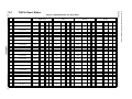
Chapter 6 Pin Reset State Table
Hardware
Initialization
Voltage
Signal (v)
Firmware
Operational
RESET
VDD33
RESET
Time
(t)
VSS
Figure 6.1 Pin Reset States
LEGEND
yes
-z
pu
pd
hw
(fw)
VDD
none
hardware enables function
hardware disables function
hardware disables output driver
hardware enables pullup
hardware enables pulldown
hardware controls function, but state is protocol dependent
firmware controls function through registers
hardware supplies power through pin, applicable only to CARD_PWR pins
hardware disables pad
Figure 6.2 Legend for Pin Reset States Table
SMSC USB2250/50i/51/51i
21
DATASHEET
Revision 1.1 (05-29-08)
Figure 6.3 USB2250/50i/51/51i Pin Reset States
Post-Reset State
xD Mode
RESET STATE
Post-Reset State
SD Mode
Post-Reset State
MS Mode
22
DATASHEET
SMSC USB2250/50i/51/51i
PIN
PIN NAME
FUNCTION
OUTPUT
PU/
PD
INPUT
FUNCTION
OUTPUT
PU/
PD
INPUT
FUNCTION
OUTPUT
PU/
PD
INPUT
85
CF_D0/GPIO16
GPIO
z
--
--
CF
hw
pd
hw
GPIO
(fw)
(fw)
(fw)
86
CF_D1/GPIO17
GPIO
z
--
--
CF
hw
pd
hw
GPIO
(fw)
(fw)
(fw)
88
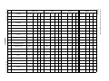
CF_D2/GPIO18
GPIO
z
--
--
CF
hw
pd
hw
GPIO
(fw)
(fw)
(fw)
59
CF_D3/GPIO19
GPIO
z
--
--
CF
hw
pd
hw
GPIO
(fw)
(fw)
(fw)
61
CF_D4/GPIO20
GPIO
z
--
--
CF
hw
pd
hw
GPIO
(fw)
(fw)
(fw)
63
CF_D5/GPIO21
GPIO
z
--
--
CF
hw
pd
hw
GPIO
(fw)
(fw)
(fw)
67
CF_D6/GPIO22
GPIO
z
--
--
CF
hw
pd
hw
GPIO
(fw)
(fw)
(fw)
69
CF_D7/GPIO23
GPIO
z
--
--
CF
hw
pd
hw
GPIO
(fw)
(fw)
(fw)
87
CF_D8/GPIO24
GPIO
z
--
--
CF
hw
pd
hw
GPIO
(fw)
(fw)
(fw)
89
CF_D9/GPIO25
GPIO
z
--
--
CF
hw
pd
hw
GPIO
(fw)
(fw)
(fw)
90
CF_D10/GPIO26
GPIO
z
--
--
CF
hw
pd
hw
GPIO
(fw)
(fw)
(fw)
60
CF_D11/GPIO27
GPIO
z
--
--
CF
hw
pd
hw
GPIO
(fw)
(fw)
(fw)
62
CF_D12/GPIO28
GPIO
z
--
--
CF
hw
pd
hw
GPIO
(fw)
(fw)
(fw)
66
CF_D13/GPIO29
GPIO
z
--
--
CF
hw
pd
hw
GPIO
(fw)
(fw)
(fw)
68
CF_D14/GPIO30
GPIO
z
--
--
CF
hw
pd
hw
GPIO
(fw)
(fw)
(fw)
70
CF_D15/GPIO31
GPIO
z
--
--
CF
hw
pd
hw
GPIO
(fw)
(fw)
(fw)
72
CF_nIOR
CF
z
--
--
CF
hw
--
--
FUNCTION
OUTPUT
PU/
PD
INPUT
Ultra Fast USB 2.0 Multi-Slot Flash Media Controller
128-Pin Reset States
Datasheet
Revision 1.1 (05-29-08)
6.1
23
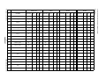
DATASHEET
SMSC USB2250/50i/51/51i
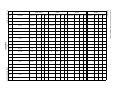
PIN
PIN NAME
FUNCTION
OUTPUT
PU/
PD
INPUT
FUNCTION
OUTPUT
PU/
PD
INPUT
73
CF_nIOW
CF
z
--
--
CF
hw
--
--
74
CF_nIRQ
CF
z
--
--
CF
z
pd
yes
79
CF_nRESET
CF
z
--
--
CF
(fw)
--
--
80
CF_IORDY
CF
z
--
--
CF
z
pu
yes
71
CF_nCS0
CF
z
--
--
CF
hw
(fw)
--
84
CF_SA0
CF
z
--
--
CF
hw
--
--
83
CF_SA1
CF
z
--
--
CF
hw
--
--
82
CF_SA2
CF
z
--
--
CF
hw
--
--
119
CF_DMACK/TXD/GPIO7
GPIO
0
--
--
CF
hw
--
117
CF_DMARQ/RXD/GPIO2
GPIO
0
--
--
CF
z
58
GPIO13(CF_nCD)
GPIO
z
pu
yes
GPIO
46
SM_D0
SM
z
pd
--
45
SM_D1
SM
z
pd
44
SM_D2
SM
z
43
SM_D3
SM
42
SM_D4
41
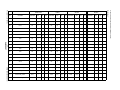
Post-Reset State
MS Mode
FUNCTION
OUTPUT
PU/
PD
INPUT
FUNCTION
OUTPUT
PU/
PD
INPUT
--
GPIO
(fw)
(fw)
(fw)
TXD
hw
--
--
pd
yes
GPIO
(fw)
(fw)
(fw)
RXD
z
(fw)
yes
(fw)
(fw)
(fw)
SM
hw
pd
yes
--
SM
hw
pd
yes
pd
--
SM
hw
pd
yes
z
pd
--
SM
hw
pd
yes
SM
z
pd
--
SM
hw
pd
yes
SM_D5
SM
z
pd
--
SM
hw
pd
yes
40
SM_D6
SM
z
pd
--
SM
hw
pd
yes
39
SM_D7
SM
z
pd
--
SM
hw
pd
yes
Ultra Fast USB 2.0 Multi-Slot Flash Media Controller
Post-Reset State
SD Mode
Datasheet
Revision 1.1 (05-29-08)
Post-Reset State
xD Mode
RESET STATE
24
DATASHEET
SMSC USB2250/50i/51/51i
PIN
PIN NAME
FUNCTION
OUTPUT
PU/
PD
INPUT
FUNCTION
OUTPUT
PU/
PD
INPUT
52
SM_ALE
SM
z
pd
--
SM
hw
pd
--
53
SM_CLE
SM
z
pd
--
SM
hw
pd
--
47
SM_nWP
SM
z
pd
--
SM
(fw)
pd
--
38
SM_nWPS
SM
z
--
--
SM
z
pu
yes
57
GPIO14(SM_nCD)
GPIO
z
pu
yes
GPIO
(fw)
(fw)
(fw)
91
MS_BS
MS
z
pd
--
MS
hw
hw
--
101
MS_SCLK
MS
z
pd
--
MS
hw
hw
--
94
MS_D0/MS_SDIO
MS
z
pd
--
MS
hw
pd
yes
92
MS_D1
MS
z
pd
--
MS
hw
hw
yes
96
MS_D2
MS
z
pd
--
MS
hw
pd
yes
99
MS_D3
MS
z
pd
--
MS
hw
pd
yes
95
MS_D4
MS
z
pd
--
MS
hw
pd
yes
93
MS_D5
MS
z
pd
--
MS
hw
hw
yes
97
MS_D6
MS
z
pd
--
MS
hw
pd
yes
100
MS_D7
MS
z
pd
--
MS
hw
pd
yes
98
GPIO12(MS_INS)
GPIO
z
pu
yes
GPIO
(fw)
(fw)
(fw)
20
SD_CMD
SD
z
--
--
SD
hw
pu
yes
18
SD_CLK
SD
z
--
--
SD
hw
--
yes
12
SD_D0
SD
z
--
--
SD
hw
pu
yes
FUNCTION
OUTPUT
PU/
PD
Post-Reset State
MS Mode
INPUT
FUNCTION
OUTPUT
PU/
PD
INPUT
Ultra Fast USB 2.0 Multi-Slot Flash Media Controller
Post-Reset State
SD Mode
Datasheet
Revision 1.1 (05-29-08)
Post-Reset State
xD Mode
RESET STATE
25
DATASHEET
SMSC USB2250/50i/51/51i
PIN
PIN NAME
FUNCTION
OUTPUT
PU/
PD
INPUT
FUNCTION
OUTPUT
PU/
PD
INPUT
10
SD_D1
SD
z
--
--
SD
hw
pu
yes
23
SD_D2
SD
z
--
--
SD
hw
pu
yes
22
SD_D3
SD
z
--
--
SD
hw
pu
yes
21
SD_D4
SD
z
--
--
SD
hw
pu
yes
19
SD_D5
SD
z
--
--
SD
hw
pu
yes
11
SD_D6
SD
z
--
--
SD
hw
pu
yes
13
SD_D7
SD
z
--
--
SD
hw
pu
yes
105
GPIO6(SD_WP)
GPIO
0
--
--
GPIO
(fw)
(fw)
(fw)
32
GPIO15(SD_nCD)
GPIO
z
pu
yes
GPIO
(fw)
(fw)
(fw)
27
MA0/CLK_SEL0
MA
z
pd
yes
MA
hw
--
--
25
MA1/CLK_SEL1
MA
z
pd
yes
MA
hw
--
--
116
MA2
MA
z
pd
yes
MA
hw
--
--
114
MA3
MA
z
pd
yes
MA
hw
--
--
112
MA4
MA
0
--
--
MA
hw
--
--
110
MA5
MA
0
--
--
MA
hw
--
--
108
MA6
MA
0
--
--
MA
hw
--
--
106
MA7
MA
0
--
--
MA
hw
--
--
109
MA8
MA
0
--
--
MA
hw
--
--
111
MA9
MA
0
--
--
MA
hw
--
--
FUNCTION
OUTPUT
PU/
PD
Post-Reset State
MS Mode
INPUT
FUNCTION
OUTPUT
PU/
PD
INPUT
Ultra Fast USB 2.0 Multi-Slot Flash Media Controller
Post-Reset State
SD Mode
Datasheet
Revision 1.1 (05-29-08)
Post-Reset State
xD Mode
RESET STATE
26
DATASHEET
SMSC USB2250/50i/51/51i
PIN
PIN NAME
FUNCTION
OUTPUT
PU/
PD
INPUT
FUNCTION
OUTPUT
PU/
PD
INPUT
24
MA10
MA
0
--
--
MA
hw
--
--
113
MA11
MA
0
--
--
MA
hw
--
--
107
MA13
MA
0
--
--
MA
hw
--
--
28
MA16
MA
0
--
--
MA
hw
--
--
37
MD0
MA
z
pu
--
MA
hw
hw
hw
36
MD1
MA
z
pu
--
MA
hw
hw
hw
35
MD2
MA
z
pu
--
MA
hw
hw
hw
34
MD3
MA
z
pu
--
MA
hw
hw
hw
31
MD4
MA
z
pu
--
MA
hw
hw
hw
30
MD5
MA
z
pu
--
MA
hw
hw
hw
29
MD6
MA
z
pu
--
MA
hw
hw
hw
33
MD7
MA
z
pu
--
MA
hw
hw
hw
115
nMRD
MA
1
--
--
MA
hw
--
--
26
nMCE
MA
1
--
--
MA
0
--
--
120
LED1 / GPIO1
GPIO
0
--
--
GPIO
(fw)
(fw)
(fw)
118
GPIO4 (SCL/xD_ID)
GPIO
0
--
--
GPIO
(fw)
(fw)
(fw)
14
GPIO8/CARD_PWR0
GPIO
z
--
--
GPIO
(fw)
(fw)
78
GPIO9/CARD_PWR1
GPIO
z
--
--
GPIO
(fw)
76
GPIO10/CARD_PWR2
GPIO
z
--
--
GPIO
(fw)
Post-Reset State
MS Mode
FUNCTION
OUTPUT
PU/
PD
INPUT
(fw)
PWR
VDD
--
--
(fw)
(fw)
PWR
VDD
--
--
(fw)
(fw)
PWR
VDD
--
--
FUNCTION
OUTPUT
PU/
PD
INPUT
Ultra Fast USB 2.0 Multi-Slot Flash Media Controller
Post-Reset State
SD Mode
Datasheet
Revision 1.1 (05-29-08)
Post-Reset State
xD Mode
RESET STATE
Post-Reset State
MS Mode
27
DATASHEET
SMSC USB2250/50i/51/51i
PIN
PIN NAME
FUNCTION
OUTPUT
PU/
PD
INPUT
FUNCTION
OUTPUT
PU/
PD
INPUT
FUNCTION
OUTPUT
PU/
PD
INPUT
16
GPIO11/CARD_PWR3
GPIO
z
--
--
GPIO
(fw)
(fw)
(fw)
PWR
VDD
--
--
103
TEST
TEST
z
--
yes
TEST
z
--
yes
64
nRESET
nRESET
z
--
yes
nRESET
z
--
yes
1
MA12
MA
0
--
--
MA
hw
--
--
4
MA14
MA
0
--
--
MA
hw
--
--
2
MA15
MA
0
--
--
MA
hw
--
--
3
nMWR
MA
1
--
--
MA
hw
--
--
121
GPIO3 (VBUS_DET)
GPIO
z
--
yes
GPIO
(fw)
(fw)
(fw)
5
GPIO5 (SDA)
GPIO
0
pu
--
GPIO
(fw)
(fw)
(fw)
55
SM_nRE
SM
z
--
--
SM
hw
(fw)
--
48
SM_nWE
SM
z
--
--
SM
hw
(fw)
--
56
SM_nB/R
SM
z
--
--
SM
z
(fw)
yes
54
SM_nCE
SM
z
--
--
SM
hw
(fw)
--
7
USB+
USB+
z
--
--
USB+
z
hw
hw
8
USB-
USB-
z
--
--
USB-
z
hw
hw
127
RBIAS
124
XTAL1(CLKIN)
123
XTAL2
6
REG_EN
FUNCTION
OUTPUT
PU/
PD
INPUT
Ultra Fast USB 2.0 Multi-Slot Flash Media Controller
Post-Reset State
SD Mode
Datasheet
Revision 1.1 (05-29-08)
Post-Reset State
xD Mode
RESET STATE
Ultra Fast USB 2.0 Multi-Slot Flash Media Controller
Datasheet
Chapter 7 DC Parameters
7.1
Maximum Guaranteed Ratings
PARAMETER
SYMBOL
MIN
Storage
Temperature
TA
-55
MAX
UNITS
150
°C
325
°C
-0.5
4.0
V
Voltage on
USB+ and
USB- pins
-0.5
(3.3V supply voltage + 2) ≤ 6
V
Voltage on
GPIO8, 9, 10
& 11
-0.5
VDD33 + 0.3
V
Voltage on any
signal pin
-0.5
VDD33 + 0.3
V
Voltage on
XTAL1
-0.5
4.0
V
Voltage on
XTAL2
-0.5
VDD18 + 0.3
V
Lead
Temperature
3.3V supply
voltage
VDD33,
VDDA33
COMMENTS
Soldering < 10 seconds
When internal power FET
operation of these pins are
enabled, these pins may be
simultaneously shorted to
ground or any voltage up to
3.63V indefinitely, without
damage to the device as long
as VDD33 and VDDA33 are less
than 3.63V and TA is less than
70oC.
Note 7.1
Stresses above the specified parameters may cause permanent damage to the device.
This is a stress rating only and functional operation of the device at any condition above
those indicated in the operation sections of this specification is not implied.
Note 7.2
When powering this device from laboratory or system power supplies, it is important that
the Absolute Maximum Ratings not be exceeded or device failure can result. Some power
supplies exhibit voltage spikes on their outputs when the AC power is switched on or off.
In addition, voltage transients on the AC power line may appear on the DC output. When
this possibility exists, it is suggested that a clamp circuit be used.
Revision 1.1 (05-29-08)
28
DATASHEET
SMSC USB2250/50i/51/51i
Ultra Fast USB 2.0 Multi-Slot Flash Media Controller
Datasheet
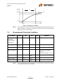
Voltage
tRT
VDD33
3.3V
100%
90%
VSS
10%
t90%
t10%
Time
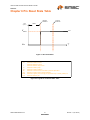
Figure 7.1 Supply Rise Time Model
Note 7.3
7.2
When powering the device, the maximum power supply ramp time should be set at a rate
faster than 400μs. This speed is important to ensure that the device resets properly.
Measure rise time at 10% and 90%.
Recommended Operating Conditions
PARAMETER
SYMBOL
MIN
MAX
UNITS
COMMENTS
Operating
Temperature
Commercial Part
TA
0
70
°C
Industrial Part
TA
-40
85
°C
3.3V supply voltage
VDD33,
VDDA33
3.0
3.6
V
(Note 7.4)
3.3V supply rise time
tRT
0
400
μs
(See Figure 7.1 and Note 7.3)
-0.3
5.5
V
If any 3.3V supply voltage drops
below 3.0V, then the MAX
becomes:
Voltage on
USB+ and USB- pins
(3.3V supply voltage) + 0.5 ≤ 5.5
Voltage on any signal
pin
-0.3
VDD33
V
Voltage on XTAL1
-0.3
VDDA33
V
Voltage on XTAL2
-0.3
VDD18
V
Note 7.4
SMSC USB2250/50i/51/51i
A 3.3V regulator with an output tolerance of 1% must be used if the output of the internal
power FET’s must support a 5% tolerance.
29
DATASHEET
Revision 1.1 (05-29-08)
Ultra Fast USB 2.0 Multi-Slot Flash Media Controller
Datasheet
7.3
DC Electrical Characteristics
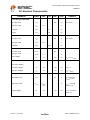
PARAMETER
SYMBOL
MIN
TYP
MAX
UNITS
0.8
V
COMMENTS
I, IPU, IPD Type Input Buffer
Low Input Level
VILI
High Input Level
VIHI
Pull Down
PD
72
μA
Pull Up
PU
58
μA
2.0
TTL Levels
V
IS Type Input Buffer
Low Input Level
VILI
High Input Level
VIHI
Hysteresis
0.8
2.0
VHYSI
V
TTL Levels
V
420
mV
ICLK Input Buffer
Low Input Level
VILCK
High Input Level
VIHCK
1.4
IIL
-10
+10
μA
Low Input Leakage
IIL
-10
+10
μA
VIN = 0
High Input Leakage
IIH
-10
+10
μA
VIN = VDD33
0.4
V
IOL = 12mA @
VDD33= 3.3V
V
IOH = -12mA @
VDD33= 3.3V
μA
VIN = 0 to VDD33
(Note 7.5)
Input Leakage
0.5
V
V
VIN = 0 to VDD33
Input Leakage
(All I and IS buffers)
O12 Type Buffer
Low Output Level
VOL
High Output Level
VOH
VDD33
- 0.4
Output Leakage
IOL
-10
Revision 1.1 (05-29-08)
30
DATASHEET
+10
SMSC USB2250/50i/51/51i
Ultra Fast USB 2.0 Multi-Slot Flash Media Controller
Datasheet
PARAMETER
SYMBOL
MIN
TYP
MAX
UNITS
COMMENTS
0.4
V
IOL = 12mA @
VDD33= 3.3V
V
IOH = -12mA @
VDD33= 3.3V
µA
VIN = 0 to VDD33
(Note 7.5)
I/O12, I/O12PU & I/O12PD Type
Buffer
Low Output Level
VOL
High Output Level
VOH
VDD33
- 0.4
Output Leakage
IOL
-10
Pull Down
PD
72
μA
Pull Up
PU
58
μA
+10
IO-U
(Note 7.6)
I-R
(Note 7.7)
I/O200
Integrated Power FET for
GPIO8, GPIO9, GPIO10, &
GPIO11
High Output Current Mode
IOUT
200
mA
VdropFET = 0.46V
Low Output Current Mode
(Note 7.8)
IOUT
100
mA
VdropFET = 0.23V
On Resistance
(Note 7.8)
RDSON
2.1
Ω
IFET = 70mA
Output Voltage Rise Time
tDSON
800
μs
CLOAD = 10μF
Supply Current Unconfigured
ICCINIT
80
90
mA
ICC
110
140
mA
ICC
135
165
mA
Supply Current Suspend
ICSBY
350
750
µA
Industrial Temperature Suspend
ICSBYI
350
950
µA
Supply Current Active
Full Speed
High Speed
VDD, VDDP = 1.8V
VDD33, VDDA = 3.3V
VDD, VDDP = 1.8V
VDD33, VDDA = 3.3V
Note 7.5
Output leakage is measured with the current pins in high impedance.
Note 7.6
See The USB 2.0 Specification, Chapter 7, for USB DC electrical characteristics
Note 7.7
RBIAS is a 3.3V tolerant analog pin.
Note 7.8
Output current range is controlled by program software, software disables FET during short
circuit condition.
SMSC USB2250/50i/51/51i
31
DATASHEET
Revision 1.1 (05-29-08)
Ultra Fast USB 2.0 Multi-Slot Flash Media Controller
Datasheet
Note 7.9
The assignment of each Integrated Card Power FET to a designated Card Connector is
controlled by both firmware and the specific board implementation. Firmware will default to
the settings listed in Table 10.1, “USB2250/50i/51/51i GPIO Usage (ROM Rev 0x00),” on
page 35.
Note 7.10 The 3.3V supply should be at least at 75% of its operating condition before the 1.8V supply
is allowed to ramp up.
7.4
Capacitance
TA = 25°C; fc = 1MHz; VDD, VDDP = 1.8V
Table 7.1 Pin Capacitance
LIMITS
PARAMETER
Clock Input Capacitance
Input Capacitance
Output Capacitance
Revision 1.1 (05-29-08)
SYMBOL
MIN
TYP
MAX
UNIT
TEST CONDITION
CXTAL
2
pF
All pins (except USB pins
and pins under test) are tied
to AC ground.
CIN
10
pF
COUT
20
pF
32
DATASHEET
SMSC USB2250/50i/51/51i
Ultra Fast USB 2.0 Multi-Slot Flash Media Controller
Datasheet
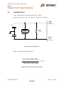
Chapter 8 AC Specifications
8.1
Oscillator/Clock
Crystal: Parallel Resonant, Fundamental Mode, 24 MHz ± 100ppm.
External Clock: 50% Duty cycle ± 10%, 24/48 MHz ± 100ppm, Jitter < 100ps rms.
XTAL1
(C S1 =
C B + C XTAL )
C1
Crystal
1Meg
CL
C2
XTAL2
(C S2 =
C B + C XTAL )
Figure 8.1 Typical Crystal Circuit
Note: CB equals total board/trace capacitance.
(C1 + CS1) x (C2 + CS2)
= CL
(C1 + CS1 + C2 + CS2)
Figure 8.2 Formula to Find Value of C1 and C2
SMSC USB2250/50i/51/51i
33
DATASHEET
Revision 1.1 (05-29-08)
R EVISION HISTORY
REVISION
-
D
5
DESCRIPTION
SEE SPECF RONT PAGE FORREVI SIONHISTORY
DATE
REL EASED BY
-
-
R1
D1
R2
3
E1/4
b
2
D 1/4
3
0.25
0°-7°
GAUGE PLANE
E1
L
E
4
L1
e
DETAIL "A"
34
DATASHEET
TOP VIEW
SEE DETAIL "A"
C
A2
A
SEAT ING PLANE
A1
c
ccc C
SIDE VIEW
NO T ES :
1. AL L D IM EN SION S AR E IN MIL LIME TE R.
2 . TR U E POSITION S PR EAD TOLE RA NC E OF EAC H L EA D IS ± 0 .0 3 5m m MAXIMU M.
3 . D IMEN SION S "D 1" A ND " E1 " DO N OT IN CL U DE M OLD PR OTRU SION S. M AX IMU M A LL OWED
P ROTR U SIO N IS 0 .2 5 mm PER SIDE .
4 . D IME NSION "L" IS M EAS UR ED AT TH E GA UGE P LA NE , 0 .25 mm A BOVE TH E SEA TIN G P LAN E.
5 . D ETA IL S ON P IN 1 ID ENTIFIER ARE OPTIONA L BU T MU ST BE L OCA TED WITH IN TH E ZONE
IN D IC ATE D.
UNLESS OT HERWISE SPECIFIED
DIMENSIONS ARE INMILLIMETERS
AND TOLERANCES ARE:
SMSC USB2250/50i/51/51i
DECIMAL
X.X
±0.1
X.XX ±0.05
X.XXX ±0.025
THI RD ANGLE PROJECT O
I N
80 ARKAY DRIVE
HAUPPAUGE, NY 11788
USA
ANGULAR
±1°
TITLE
INTERPRET DIM ANDT OL PER
ASME Y14.5 M- 1994
MATERIAL
-
3-D VIEW
NAME
DATE
DRAWN
FINISH
S. K. ILI EV
12/17/04
DWG NUMBER
CHECKED
PRINT WITH "SCALE TO FIT"
DO NOT SCALE DRAWING
S. K. ILI EV
SCALE
12/17/04
REV
MO-128-VTQFP-14x14x1.0
12/17/04
APPROVED
S. K. ILI EV
PACKAGE OUTLINE
128 VTQFP-14x14x1.0mm BODY-0.4mm PITCH
1:1
Figure 9.1 USB2250/50i/51/51i 128-Pin VTQFP, 14x14x1.0mm Body, 2.0mm Pitch
STD COMPLIANCE
JE DEC: MS -026 (D)
C
SHEET
1 OF 1
Ultra Fast USB 2.0 Multi-Slot Flash Media Controller
Datasheet
Revision 1.1 (05-29-08)
Chapter 9 Package Outline
Ultra Fast USB 2.0 Multi-Slot Flash Media Controller
Datasheet
Chapter 10 GPIO Usage
Table 10.1 USB2250/50i/51/51i GPIO Usage (ROM Rev 0x00)
NAME
ACTIVE LEVEL
GPIO1
H
LED1
LED indicator
GPIO2
H
CF_DMARQ / RXD
Compact Flash DMA request / Receive
Port of Debugger
GPIO3
H
VBUS_DET
USB Vbus detect
GPIO4
H
SCL / xD_ID
Serial EEPROM clock output / xD card
detect
GPIO5
H
SDA
Serial EEPROM data
GPIO6
L
SD_WP
SD Write Protect
GPIO7
H
CF_DMACK / TXD
Compact Flash DMA acknowledge
/Transmit Port of Debugger
GPIO8
L
CRD_PWR0
Card Power Control
GPIO9
L
CRD_PWR1
Card Power Control
GPIO10
L
CRD_PWR2
Card Power Control
GPIO11
L
CRD_PWR3
Card Power Control
GPIO12
L
MS_INS
Memory Stick Card Insertion
GPIO13
L
CF_nCD
Compact Flash card detect
GPIO14
L
xD_nCD
xD card detect
GPIO15
L
SD_nCD
Secure Digital card detect
GPIO16-32
USER
GPIO [32:16]
User defined
SMSC USB2250/50i/51/51i
SYMBOL
35
DATASHEET
DESCRIPTION AND NOTE
Revision 1.1 (05-29-08)