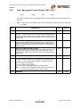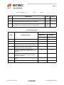
1
LAN9420/LAN9420i
Single-Chip Ethernet Controller
with HP Auto-MDIX Support
and PCI Interface
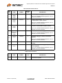
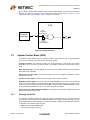
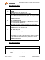
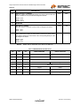
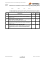
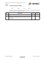
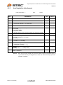
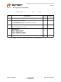
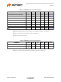
PRODUCT FEATURES
Datasheet
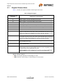
Highlights
Optimized for embedded applications with 32-bit
RISC CPUs
Integrated descriptor based scatter-gather DMA and
IRQ deassertion timer effectively increase network
throughput and reduce CPU loading
Integrated Ethernet MAC with full-duplex support
Integrated 10/100 Ethernet PHY with HP Auto-MDIX
support
32-bit, 33MHz, PCI 3.0 compliant interface
Reduced power operating modes with PCI Power
Management Specification 1.1 compliance
Supports multiple audio & video streams over
Ethernet
—
—
—
—
Cable, satellite, and IP set-top boxes
Digital televisions
Digital video recorders
Home gateways
Digital media clients/servers
Industrial automation systems
Industrial/single board PC
Kiosk/POS enterprise equipment
Integrated High-Performance 10/100 Ethernet
Controller
—
—
—
—
—
—
—
—
—
—
Fully compliant with IEEE802.3/802.3u
Integrated Ethernet MAC and PHY
10BASE-T and 100BASE-TX support
Full- and half-duplex support
Full-duplex flow control
Preamble generation and removal
Automatic 32-bit CRC generation and checking
Automatic payload padding and pad removal
Loop-back modes
Flexible address filtering modes
– One 48-bit perfect address
– 64 hash-filtered multicast addresses
– Pass all multicast
SMSC LAN9420/LAN9420i
Comprehensive Power Management Features
— Supports PCI Bus Power Management Interface
Specification, Revision 1.1
— Supports optional wake from D3cold
(via configuration strap option when Vaux is available)
— Wake on LAN
— Wake on link status change (energy detect)
— Magic packet wakeup
General Purpose I/O
— 3 programmable GPIO pins
— 2 GPO pins
Support for Optional EEPROM
— Serial interface provided for EEPROM
— Used to store PCI and MAC address configuration
values
Key Benefits
PCI Interface
— PCI Local Bus Specification Revision 3.0 compliant
— 32-bit/33-MHz PCI bus
— Descriptor based scatter-gather DMA enables zerocopy drivers
Target Applications
– Promiscuous mode
– Inverse filtering
– Pass all incoming with status report
Wakeup packet support
Integrated 10/100 Ethernet PHY
– Auto-negotiation
– Automatic polarity detection and correction
– Supports HP Auto-MDIX
– Supports energy-detect power down
Support for 3 status LEDs
Receive and transmit TCP checksum offload
Miscellaneous Features
— Big/Little/Mixed endian support for registers,
descriptors, and buffers
— IRQ deassertion timer
— General purpose timer
Single 3.3V Power Supply
Packaging
— Integrated 1.8V regulator
— Available in 128-pin VTQFP Lead-free RoHS Compliant
package
Environmental
— Available in commercial & industrial temperature ranges
DATASHEET
Revision 1.22 (09-25-08)
Single-Chip Ethernet Controller with HP Auto-MDIX Support and PCI Interface
Datasheet
ORDER NUMBERS:
LAN9420-NU FOR 128-PIN VTQFP, LEAD-FREE ROHS COMPLIANT PACKAGE (0 TO 70oC)
LAN9420i-NU FOR 128-PIN VTQFP, LEAD-FREE ROHS COMPLIANT PACKAGE (-40o TO 85oC)
80 ARKAY DRIVE, HAUPPAUGE, NY 11788 (631) 435-6000, FAX (631) 273-3123
Copyright © 2008 SMSC or its subsidiaries. All rights reserved.
Circuit diagrams and other information relating to SMSC products are included as a means of illustrating typical applications. Consequently, complete information sufficient for
construction purposes is not necessarily given. Although the information has been checked and is believed to be accurate, no responsibility is assumed for inaccuracies. SMSC
reserves the right to make changes to specifications and product descriptions at any time without notice. Contact your local SMSC sales office to obtain the latest specifications
before placing your product order. The provision of this information does not convey to the purchaser of the described semiconductor devices any licenses under any patent
rights or other intellectual property rights of SMSC or others. All sales are expressly conditional on your agreement to the terms and conditions of the most recently dated
version of SMSC's standard Terms of Sale Agreement dated before the date of your order (the "Terms of Sale Agreement"). The product may contain design defects or errors
known as anomalies which may cause the product's functions to deviate from published specifications. Anomaly sheets are available upon request. SMSC products are not
designed, intended, authorized or warranted for use in any life support or other application where product failure could cause or contribute to personal injury or severe property
damage. Any and all such uses without prior written approval of an Officer of SMSC and further testing and/or modification will be fully at the risk of the customer. Copies of
this document or other SMSC literature, as well as the Terms of Sale Agreement, may be obtained by visiting SMSC’s website at http://www.smsc.com. SMSC is a registered
trademark of Standard Microsystems Corporation (“SMSC”). Product names and company names are the trademarks of their respective holders.
SMSC DISCLAIMS AND EXCLUDES ANY AND ALL WARRANTIES, INCLUDING WITHOUT LIMITATION ANY AND ALL IMPLIED WARRANTIES OF MERCHANTABILITY,
FITNESS FOR A PARTICULAR PURPOSE, TITLE, AND AGAINST INFRINGEMENT AND THE LIKE, AND ANY AND ALL WARRANTIES ARISING FROM ANY COURSE
OF DEALING OR USAGE OF TRADE. IN NO EVENT SHALL SMSC BE LIABLE FOR ANY DIRECT, INCIDENTAL, INDIRECT, SPECIAL, PUNITIVE, OR CONSEQUENTIAL
DAMAGES; OR FOR LOST DATA, PROFITS, SAVINGS OR REVENUES OF ANY KIND; REGARDLESS OF THE FORM OF ACTION, WHETHER BASED ON CONTRACT;
TORT; NEGLIGENCE OF SMSC OR OTHERS; STRICT LIABILITY; BREACH OF WARRANTY; OR OTHERWISE; WHETHER OR NOT ANY REMEDY OF BUYER IS HELD
TO HAVE FAILED OF ITS ESSENTIAL PURPOSE, AND WHETHER OR NOT SMSC HAS BEEN ADVISED OF THE POSSIBILITY OF SUCH DAMAGES.
Revision 1.22 (09-25-08)
2
DATASHEET
SMSC LAN9420/LAN9420i
Single-Chip Ethernet Controller with HP Auto-MDIX Support and PCI Interface
Datasheet
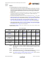
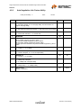
Table of Contents
Chapter 1 Introduction . . . . . . . . . . . . . . . . . . . . . . . . . . . . . . . . . . . . . . . . . . . . . . . . . . . . . . 11
1.1
1.2
1.3
1.4
1.5
1.6
1.7
1.8
Block Diagrams. . . . . . . . . . . . . . . . . . . . . . . . . . . . . . . . . . . . . . . . . . . . . . . . . . . . . . . . . . . . . . . .
General Description . . . . . . . . . . . . . . . . . . . . . . . . . . . . . . . . . . . . . . . . . . . . . . . . . . . . . . . . . . . .
PCI Bridge . . . . . . . . . . . . . . . . . . . . . . . . . . . . . . . . . . . . . . . . . . . . . . . . . . . . . . . . . . . . . . . . . . .
DMA Controller . . . . . . . . . . . . . . . . . . . . . . . . . . . . . . . . . . . . . . . . . . . . . . . . . . . . . . . . . . . . . . . .
Ethernet MAC . . . . . . . . . . . . . . . . . . . . . . . . . . . . . . . . . . . . . . . . . . . . . . . . . . . . . . . . . . . . . . . . .
Ethernet PHY . . . . . . . . . . . . . . . . . . . . . . . . . . . . . . . . . . . . . . . . . . . . . . . . . . . . . . . . . . . . . . . . .
System Control Block . . . . . . . . . . . . . . . . . . . . . . . . . . . . . . . . . . . . . . . . . . . . . . . . . . . . . . . . . . .
1.7.1
Interrupt Controller. . . . . . . . . . . . . . . . . . . . . . . . . . . . . . . . . . . . . . . . . . . . . . . . . . . . . .
1.7.2
PLL and Power Management . . . . . . . . . . . . . . . . . . . . . . . . . . . . . . . . . . . . . . . . . . . . .
1.7.3
EEPROM Controller . . . . . . . . . . . . . . . . . . . . . . . . . . . . . . . . . . . . . . . . . . . . . . . . . . . .
1.7.4
GPIO/LED Controller . . . . . . . . . . . . . . . . . . . . . . . . . . . . . . . . . . . . . . . . . . . . . . . . . . . .
1.7.5
General Purpose Timer . . . . . . . . . . . . . . . . . . . . . . . . . . . . . . . . . . . . . . . . . . . . . . . . . .
1.7.6
Free Run Counter . . . . . . . . . . . . . . . . . . . . . . . . . . . . . . . . . . . . . . . . . . . . . . . . . . . . . .
Control and Status Registers (CSR). . . . . . . . . . . . . . . . . . . . . . . . . . . . . . . . . . . . . . . . . . . . . . . .
11
12
13
13
13
13
13
13
14
14
14
14
14
14
Chapter 2 Pin Description and Configuration . . . . . . . . . . . . . . . . . . . . . . . . . . . . . . . . . . . 15
2.1
2.2
Pin List . . . . . . . . . . . . . . . . . . . . . . . . . . . . . . . . . . . . . . . . . . . . . . . . . . . . . . . . . . . . . . . . . . . . . . 16
Buffer Types . . . . . . . . . . . . . . . . . . . . . . . . . . . . . . . . . . . . . . . . . . . . . . . . . . . . . . . . . . . . . . . . . . 22
Chapter 3 Functional Description . . . . . . . . . . . . . . . . . . . . . . . . . . . . . . . . . . . . . . . . . . . . . 23
3.1
3.2
3.3
3.4
Functional Overview . . . . . . . . . . . . . . . . . . . . . . . . . . . . . . . . . . . . . . . . . . . . . . . . . . . . . . . . . . . . 23
PCI Bridge (PCIB). . . . . . . . . . . . . . . . . . . . . . . . . . . . . . . . . . . . . . . . . . . . . . . . . . . . . . . . . . . . . . 23
3.2.1
PCI Bridge (PCIB) Block Diagram . . . . . . . . . . . . . . . . . . . . . . . . . . . . . . . . . . . . . . . . . . 24
3.2.2
PCI Interface Environments. . . . . . . . . . . . . . . . . . . . . . . . . . . . . . . . . . . . . . . . . . . . . . . 25
3.2.3
PCI Master Interface . . . . . . . . . . . . . . . . . . . . . . . . . . . . . . . . . . . . . . . . . . . . . . . . . . . . 25
3.2.3.1 PCI Master Transaction Errors....................................................................................... 25
3.2.4
PCI Target Interface . . . . . . . . . . . . . . . . . . . . . . . . . . . . . . . . . . . . . . . . . . . . . . . . . . . . 26
3.2.4.1 PCI Configuration Space Registers ............................................................................... 26
3.2.4.2 Control and Status Registers (CSR) .............................................................................. 26
3.2.4.2.1 CSR Endianness....................................................................................................... 26
3.2.4.2.2 I/O Mapping of CSR.................................................................................................. 27
3.2.4.3 PCI Target Interface Transaction Errors ........................................................................ 27
3.2.4.4 PCI Discard Timer.......................................................................................................... 27
3.2.5
Interrupt Gating Logic . . . . . . . . . . . . . . . . . . . . . . . . . . . . . . . . . . . . . . . . . . . . . . . . . . . 27
System Control Block (SCB). . . . . . . . . . . . . . . . . . . . . . . . . . . . . . . . . . . . . . . . . . . . . . . . . . . . . . 28
3.3.1
Interrupt Controller. . . . . . . . . . . . . . . . . . . . . . . . . . . . . . . . . . . . . . . . . . . . . . . . . . . . . . 28
3.3.2
Wake Event Detection Logic . . . . . . . . . . . . . . . . . . . . . . . . . . . . . . . . . . . . . . . . . . . . . . 30
3.3.3
General Purpose Timer (GPT). . . . . . . . . . . . . . . . . . . . . . . . . . . . . . . . . . . . . . . . . . . . . 30
3.3.4
Free-Run Counter (FRC) . . . . . . . . . . . . . . . . . . . . . . . . . . . . . . . . . . . . . . . . . . . . . . . . . 31
3.3.5
EEPROM Controller (EPC) . . . . . . . . . . . . . . . . . . . . . . . . . . . . . . . . . . . . . . . . . . . . . . . 31
3.3.5.1 EEPROM Format ...........................................................................................................31
3.3.5.2 MAC Address, Subsystem ID, and Subsystem Vendor ID Auto-Load ........................... 32
3.3.5.3 EEPROM Host Operations............................................................................................. 32
3.3.5.3.1 Supported EEPROM Operations .............................................................................. 33
3.3.5.3.2 Host Initiated MAC Address, SSID, SSVID Reload .................................................. 37
3.3.5.3.3 EEPROM Command and Data Registers .................................................................37
3.3.5.3.4 EEPROM Timing....................................................................................................... 37
3.3.6
System Control and Status Registers (SCSR) . . . . . . . . . . . . . . . . . . . . . . . . . . . . . . . . 38
DMA Controller (DMAC) . . . . . . . . . . . . . . . . . . . . . . . . . . . . . . . . . . . . . . . . . . . . . . . . . . . . . . . . . 38
3.4.1
DMA Controller Architecture . . . . . . . . . . . . . . . . . . . . . . . . . . . . . . . . . . . . . . . . . . . . . . 38
SMSC LAN9420/LAN9420i
3
DATASHEET
Revision 1.22 (09-25-08)
Single-Chip Ethernet Controller with HP Auto-MDIX Support and PCI Interface
Datasheet
3.5
3.6
3.4.2
Data Descriptors and Buffers . . . . . . . . . . . . . . . . . . . . . . . . . . . . . . . . . . . . . . . . . . . . . 38
3.4.2.1 Receive Descriptors ....................................................................................................... 41
3.4.2.2 Transmit descriptors....................................................................................................... 45
3.4.3
Initialization . . . . . . . . . . . . . . . . . . . . . . . . . . . . . . . . . . . . . . . . . . . . . . . . . . . . . . . . . . . 49
3.4.4
Transmit Operation . . . . . . . . . . . . . . . . . . . . . . . . . . . . . . . . . . . . . . . . . . . . . . . . . . . . . 50
3.4.5
Receive Operation . . . . . . . . . . . . . . . . . . . . . . . . . . . . . . . . . . . . . . . . . . . . . . . . . . . . . . 50
3.4.6
Receive Descriptor Acquisition . . . . . . . . . . . . . . . . . . . . . . . . . . . . . . . . . . . . . . . . . . . . 50
3.4.7
Suspend State Behavior . . . . . . . . . . . . . . . . . . . . . . . . . . . . . . . . . . . . . . . . . . . . . . . . . 51
3.4.7.1 Transmit Engine ............................................................................................................. 51
3.4.7.2 Receive Engine .............................................................................................................. 51
3.4.8
Stopping Transmission and Reception . . . . . . . . . . . . . . . . . . . . . . . . . . . . . . . . . . . . . . 51
3.4.9
TX Buffer Fragmentation Rules . . . . . . . . . . . . . . . . . . . . . . . . . . . . . . . . . . . . . . . . . . . . 52
3.4.9.1 Calculating Worst-Case TX FIFO (MIL) Usage.............................................................. 52
3.4.10 DMAC Interrupts . . . . . . . . . . . . . . . . . . . . . . . . . . . . . . . . . . . . . . . . . . . . . . . . . . . . . . . 52
3.4.11 DMAC Control and Status Registers (DCSR) . . . . . . . . . . . . . . . . . . . . . . . . . . . . . . . . . 52
10/100 Ethernet MAC . . . . . . . . . . . . . . . . . . . . . . . . . . . . . . . . . . . . . . . . . . . . . . . . . . . . . . . . . . . 53
3.5.1
Flow Control . . . . . . . . . . . . . . . . . . . . . . . . . . . . . . . . . . . . . . . . . . . . . . . . . . . . . . . . . . 54
3.5.1.1 Full-Duplex Flow Control................................................................................................54
3.5.2
Virtual Local Area Network (VLAN) Support . . . . . . . . . . . . . . . . . . . . . . . . . . . . . . . . . . 54
3.5.3
Address Filtering Functional Description . . . . . . . . . . . . . . . . . . . . . . . . . . . . . . . . . . . . . 55
3.5.3.1 Perfect Filtering .............................................................................................................. 56
3.5.3.2 Hash Only Filtering Mode............................................................................................... 56
3.5.3.3 Hash Perfect Filtering .................................................................................................... 56
3.5.3.4 Inverse Filtering ............................................................................................................. 56
3.5.4
Wakeup Frame Detection . . . . . . . . . . . . . . . . . . . . . . . . . . . . . . . . . . . . . . . . . . . . . . . . 57
3.5.4.1 Magic Packet Detection ................................................................................................. 59
3.5.5
Receive Checksum Offload Engine (RXCOE). . . . . . . . . . . . . . . . . . . . . . . . . . . . . . . . . 60
3.5.5.1 RX Checksum Calculation ............................................................................................. 63
3.5.6
Transmit Checksum Offload Engine (TXCOE) . . . . . . . . . . . . . . . . . . . . . . . . . . . . . . . . 63
3.5.6.1 TX Checksum Calculation..............................................................................................64
3.5.7
MAC Control and Status Registers (MCSR) . . . . . . . . . . . . . . . . . . . . . . . . . . . . . . . . . . 64
10/100 Ethernet PHY . . . . . . . . . . . . . . . . . . . . . . . . . . . . . . . . . . . . . . . . . . . . . . . . . . . . . . . . . . . 64
3.6.1
100BASE-TX Transmit . . . . . . . . . . . . . . . . . . . . . . . . . . . . . . . . . . . . . . . . . . . . . . . . . . 65
3.6.1.1 4B/5B Encoding ............................................................................................................. 65
3.6.1.2 Scrambling ..................................................................................................................... 66
3.6.1.3 NRZI and MLT3 Encoding ............................................................................................. 67
3.6.1.4 100M Transmit Driver..................................................................................................... 67
3.6.1.5 100M Phase Lock Loop (PLL) ....................................................................................... 67
3.6.2
100BASE-TX Receive . . . . . . . . . . . . . . . . . . . . . . . . . . . . . . . . . . . . . . . . . . . . . . . . . . . 67
3.6.2.1 100M Receive Input ....................................................................................................... 67
3.6.2.2 Equalizer, Baseline Wander Correction and Clock and Data Recovery ........................ 67
3.6.2.3 NRZI and MLT-3 Decoding ............................................................................................ 68
3.6.2.4 Descrambling ................................................................................................................. 68
3.6.2.5 Alignment ....................................................................................................................... 68
3.6.2.6 5B/4B Decoding ............................................................................................................. 68
3.6.2.7 Receiver Errors .............................................................................................................. 68
3.6.3
10BASE-T Transmit. . . . . . . . . . . . . . . . . . . . . . . . . . . . . . . . . . . . . . . . . . . . . . . . . . . . . 69
3.6.3.1 10M Transmit Data Across the Internal MII Bus ............................................................ 69
3.6.3.2 Manchester Encoding .................................................................................................... 69
3.6.3.3 10M Transmit Drivers..................................................................................................... 69
3.6.4
10BASE-T Receive . . . . . . . . . . . . . . . . . . . . . . . . . . . . . . . . . . . . . . . . . . . . . . . . . . . . . 69
3.6.4.1 10M Receive Input and Squelch .................................................................................... 69
3.6.4.2 Manchester Decoding .................................................................................................... 69
3.6.4.3 Jabber Detection ............................................................................................................ 70
3.6.5
Auto-negotiation . . . . . . . . . . . . . . . . . . . . . . . . . . . . . . . . . . . . . . . . . . . . . . . . . . . . . . . 70
Revision 1.22 (09-25-08)
4
DATASHEET
SMSC LAN9420/LAN9420i
Single-Chip Ethernet Controller with HP Auto-MDIX Support and PCI Interface
Datasheet
3.7
3.6.6
Parallel Detection . . . . . . . . . . . . . . . . . . . . . . . . . . . . . . . . . . . . . . . . . . . . . . . . . . . . . . 71
3.6.6.1 Re-starting Auto-negotiation .......................................................................................... 71
3.6.6.2 Disabling Auto-negotiation ............................................................................................. 71
3.6.6.3 Half vs. Full-Duplex ........................................................................................................ 72
3.6.7
HP Auto-MDIX . . . . . . . . . . . . . . . . . . . . . . . . . . . . . . . . . . . . . . . . . . . . . . . . . . . . . . . . . 72
3.6.8
PHY Power-Down Modes . . . . . . . . . . . . . . . . . . . . . . . . . . . . . . . . . . . . . . . . . . . . . . . . 72
3.6.8.1 General Power-Down..................................................................................................... 72
3.6.8.2 Energy Detect Power-Down........................................................................................... 73
3.6.9
PHY Resets . . . . . . . . . . . . . . . . . . . . . . . . . . . . . . . . . . . . . . . . . . . . . . . . . . . . . . . . . . . 73
3.6.9.1 PHY Soft Reset via PMT_CTRL bit 10 (PHY_RST)....................................................... 73
3.6.9.2 PHY Soft Reset via PHY Basic Control Register bit 15 (PHY Reg. 0.15) ...................... 73
3.6.10 Required Ethernet Magnetics . . . . . . . . . . . . . . . . . . . . . . . . . . . . . . . . . . . . . . . . . . . . . 73
3.6.11 PHY Registers . . . . . . . . . . . . . . . . . . . . . . . . . . . . . . . . . . . . . . . . . . . . . . . . . . . . . . . . . 73
Power Management . . . . . . . . . . . . . . . . . . . . . . . . . . . . . . . . . . . . . . . . . . . . . . . . . . . . . . . . . . . . 73
3.7.1
Overview . . . . . . . . . . . . . . . . . . . . . . . . . . . . . . . . . . . . . . . . . . . . . . . . . . . . . . . . . . . . . 73
3.7.2
Related External Signals and Power Supplies . . . . . . . . . . . . . . . . . . . . . . . . . . . . . . . . 74
3.7.3
Device Clocking . . . . . . . . . . . . . . . . . . . . . . . . . . . . . . . . . . . . . . . . . . . . . . . . . . . . . . . . 75
3.7.4
Power States . . . . . . . . . . . . . . . . . . . . . . . . . . . . . . . . . . . . . . . . . . . . . . . . . . . . . . . . . . 75
3.7.4.1 G3 State (Mechanical Off) ............................................................................................. 75
3.7.4.1.1 Power Management Events in G3 ................................................................................................. 75
3.7.4.1.2 Exiting the G3 State ..................................................................................................76
3.7.4.2 D0UNINTIALIZED State (D0U) ...................................................................................... 76
3.7.4.2.1 Exiting the D0U State................................................................................................ 76
3.7.4.3 D0ACTIVE State (D0A).................................................................................................. 76
3.7.4.3.1 Power Management Events in D0A............................................................................................... 76
3.7.4.3.2 Exiting the D0A State................................................................................................ 77
3.7.4.4 The D3HOT State .......................................................................................................... 77
3.7.4.4.1 Power Management Events in D3HOT.......................................................................................... 77
3.7.4.4.2 Exiting the D3HOT State........................................................................................... 77
3.7.4.5 The D3COLD State ........................................................................................................78
3.7.4.5.1 Power Management Events in D3COLD ....................................................................................... 78
3.7.4.5.2 Exiting the D3COLD State ........................................................................................ 78
3.7.5
Resets . . . . . . . . . . . . . . . . . . . . . . . . . . . . . . . . . . . . . . . . . . . . . . . . . . . . . . . . . . . . . . . 79
3.7.5.1 PHY Resets ................................................................................................................... 80
3.7.6
Detecting Power Management Events . . . . . . . . . . . . . . . . . . . . . . . . . . . . . . . . . . . . . . 80
3.7.6.1 Enabling Wakeup Frame Wake Events ......................................................................... 81
3.7.7
Enabling Link Status Change (Energy Detect) Wake Events . . . . . . . . . . . . . . . . . . . . . 81
Chapter 4 Register Descriptions . . . . . . . . . . . . . . . . . . . . . . . . . . . . . . . . . . . . . . . . . . . . . . . 83
4.1
4.2
4.3
Register Nomenclature . . . . . . . . . . . . . . . . . . . . . . . . . . . . . . . . . . . . . . . . . . . . . . . . . . . . . . . . . . 85
System Control and Status Registers (SCSR) . . . . . . . . . . . . . . . . . . . . . . . . . . . . . . . . . . . . . . . . 86
4.2.1
ID and Revision (ID_REV) . . . . . . . . . . . . . . . . . . . . . . . . . . . . . . . . . . . . . . . . . . . . . . . . 87
4.2.2
Interrupt Control Register (INT_CTL) . . . . . . . . . . . . . . . . . . . . . . . . . . . . . . . . . . . . . . . 88
4.2.3
Interrupt Status Register (INT_STS) . . . . . . . . . . . . . . . . . . . . . . . . . . . . . . . . . . . . . . . . 89
4.2.4
Interrupt Configuration Register (INT_CFG) . . . . . . . . . . . . . . . . . . . . . . . . . . . . . . . . . . 91
4.2.5
General Purpose Input/Output Configuration Register (GPIO_CFG) . . . . . . . . . . . . . . . 92
4.2.6
General Purpose Timer Configuration Register (GPT_CFG) . . . . . . . . . . . . . . . . . . . . . 94
4.2.7
General Purpose Timer Current Count Register (GPT_CNT) . . . . . . . . . . . . . . . . . . . . . 95
4.2.8
Bus Master Bridge Configuration Register (BUS_CFG) . . . . . . . . . . . . . . . . . . . . . . . . . 96
4.2.9
Power Management Control Register (PMT_CTRL) . . . . . . . . . . . . . . . . . . . . . . . . . . . . 97
4.2.10 Free Run Counter (FREE_RUN) . . . . . . . . . . . . . . . . . . . . . . . . . . . . . . . . . . . . . . . . . . . 98
4.2.11 EEPROM Command Register (E2P_CMD). . . . . . . . . . . . . . . . . . . . . . . . . . . . . . . . . . . 99
4.2.12 EEPROM Data Register (E2P_DATA) . . . . . . . . . . . . . . . . . . . . . . . . . . . . . . . . . . . . . 102
DMAC Control and Status Registers (DCSR). . . . . . . . . . . . . . . . . . . . . . . . . . . . . . . . . . . . . . . . 103
4.3.1
Bus Mode Register (BUS_MODE). . . . . . . . . . . . . . . . . . . . . . . . . . . . . . . . . . . . . . . . . 104
SMSC LAN9420/LAN9420i
5
DATASHEET
Revision 1.22 (09-25-08)
Single-Chip Ethernet Controller with HP Auto-MDIX Support and PCI Interface
Datasheet
4.4
4.5
4.6
4.3.2
Transmit Poll Demand Register (TX_POLL_DEMAND) . . . . . . . . . . . . . . . . . . . . . . . .
4.3.3
Receive Poll Demand Register (RX_POLL_DEMAND). . . . . . . . . . . . . . . . . . . . . . . . .
4.3.4
Receive List Base Address Register (RX_BASE_ADDR) . . . . . . . . . . . . . . . . . . . . . . .
4.3.5
Transmit List Base Address Register (TX_BASE_ADDR). . . . . . . . . . . . . . . . . . . . . . .
4.3.6
DMA Controller Status Register (DMAC_STATUS) . . . . . . . . . . . . . . . . . . . . . . . . . . .
4.3.7
DMA Controller Control (Operation Mode) Register (DMAC_CONTROL) . . . . . . . . . .
4.3.8
DMA Controller Interrupt Enable Register (DMAC_INTR_ENA) . . . . . . . . . . . . . . . . . .
4.3.9
Missed Frame and Buffer Overflow Counter Reg (MISS_FRAME_CNTR) . . . . . . . . . .
4.3.10 Current Transmit Buffer Address Register (TX_BUFF_ADDR) . . . . . . . . . . . . . . . . . . .
4.3.11 Current Receive Buffer Address Register (RX_BUFF_ADDR) . . . . . . . . . . . . . . . . . . .
MAC Control and Status Registers (MCSR). . . . . . . . . . . . . . . . . . . . . . . . . . . . . . . . . . . . . . . . .
4.4.1
MAC Control Register (MAC_CR) . . . . . . . . . . . . . . . . . . . . . . . . . . . . . . . . . . . . . . . . .
4.4.2
MAC Address High Register (ADDRH) . . . . . . . . . . . . . . . . . . . . . . . . . . . . . . . . . . . . .
4.4.3
MAC Address Low Register (ADDRL) . . . . . . . . . . . . . . . . . . . . . . . . . . . . . . . . . . . . . .
4.4.4
Multicast Hash Table High Register (HASHH) . . . . . . . . . . . . . . . . . . . . . . . . . . . . . . .
4.4.5
Multicast Hash Table Low Register (HASHL) . . . . . . . . . . . . . . . . . . . . . . . . . . . . . . . .
4.4.6
MII Access Register (MII_ACCESS) . . . . . . . . . . . . . . . . . . . . . . . . . . . . . . . . . . . . . . .
4.4.7
MII Data Register (MII_DATA). . . . . . . . . . . . . . . . . . . . . . . . . . . . . . . . . . . . . . . . . . . .
4.4.8
Flow Control Register (FLOW) . . . . . . . . . . . . . . . . . . . . . . . . . . . . . . . . . . . . . . . . . . .
4.4.9
VLAN1 Tag Register (VLAN1) . . . . . . . . . . . . . . . . . . . . . . . . . . . . . . . . . . . . . . . . . . . .
4.4.10 VLAN2 Tag Register (VLAN2) . . . . . . . . . . . . . . . . . . . . . . . . . . . . . . . . . . . . . . . . . . . .
4.4.11 Wakeup Frame Filter (WUFF) . . . . . . . . . . . . . . . . . . . . . . . . . . . . . . . . . . . . . . . . . . . .
4.4.12 Wakeup Control and Status Register (WUCSR) . . . . . . . . . . . . . . . . . . . . . . . . . . . . . .
4.4.13 Checksum Offload Engine Control Register (COE_CR) . . . . . . . . . . . . . . . . . . . . . . . .
PHY Registers . . . . . . . . . . . . . . . . . . . . . . . . . . . . . . . . . . . . . . . . . . . . . . . . . . . . . . . . . . . . . . .
4.5.1
Basic Control Register . . . . . . . . . . . . . . . . . . . . . . . . . . . . . . . . . . . . . . . . . . . . . . . . . .
4.5.2
Basic Status Register . . . . . . . . . . . . . . . . . . . . . . . . . . . . . . . . . . . . . . . . . . . . . . . . . .
4.5.3
PHY Identifier 1 . . . . . . . . . . . . . . . . . . . . . . . . . . . . . . . . . . . . . . . . . . . . . . . . . . . . . . .
4.5.4
PHY Identifier 2 . . . . . . . . . . . . . . . . . . . . . . . . . . . . . . . . . . . . . . . . . . . . . . . . . . . . . . .
4.5.5
Auto Negotiation Advertisement . . . . . . . . . . . . . . . . . . . . . . . . . . . . . . . . . . . . . . . . . .
4.5.6
Auto Negotiation Link Partner Ability . . . . . . . . . . . . . . . . . . . . . . . . . . . . . . . . . . . . . . .
4.5.7
Auto Negotiation Expansion . . . . . . . . . . . . . . . . . . . . . . . . . . . . . . . . . . . . . . . . . . . . .
4.5.8
Mode Control/Status . . . . . . . . . . . . . . . . . . . . . . . . . . . . . . . . . . . . . . . . . . . . . . . . . . .
4.5.9
Special Modes . . . . . . . . . . . . . . . . . . . . . . . . . . . . . . . . . . . . . . . . . . . . . . . . . . . . . . . .
4.5.10 Special Control/Status Indications . . . . . . . . . . . . . . . . . . . . . . . . . . . . . . . . . . . . . . . . .
4.5.11 Interrupt Source Flag . . . . . . . . . . . . . . . . . . . . . . . . . . . . . . . . . . . . . . . . . . . . . . . . . . .
4.5.12 Interrupt Mask . . . . . . . . . . . . . . . . . . . . . . . . . . . . . . . . . . . . . . . . . . . . . . . . . . . . . . . .
4.5.13 PHY Special Control/Status. . . . . . . . . . . . . . . . . . . . . . . . . . . . . . . . . . . . . . . . . . . . . .
PCI Configuration Space CSR (CONFIG CSR) . . . . . . . . . . . . . . . . . . . . . . . . . . . . . . . . . . . . . .
4.6.1
PCI Power Management Capabilities Register (PCI_PMC) . . . . . . . . . . . . . . . . . . . . .
4.6.2
PCI Power Management Control and Status Register (PCI_PMCSR) . . . . . . . . . . . . .
105
106
107
108
109
111
113
115
116
117
118
119
123
124
125
126
127
128
129
130
131
132
133
134
135
136
137
138
139
140
141
142
143
144
145
146
147
148
149
151
153
Chapter 5 Operational Characteristics . . . . . . . . . . . . . . . . . . . . . . . . . . . . . . . . . . . . . . . . 155
5.1
5.2
5.3
5.4
5.5
5.6
Absolute Maximum Ratings*. . . . . . . . . . . . . . . . . . . . . . . . . . . . . . . . . . . . . . . . . . . . . . . . . . . . .
Operating Conditions** . . . . . . . . . . . . . . . . . . . . . . . . . . . . . . . . . . . . . . . . . . . . . . . . . . . . . . . . .
Power Consumption . . . . . . . . . . . . . . . . . . . . . . . . . . . . . . . . . . . . . . . . . . . . . . . . . . . . . . . . . . .
5.3.1
D0 - Normal Operation with Ethernet Traffic . . . . . . . . . . . . . . . . . . . . . . . . . . . . . . . . .
5.3.2
D3 - Enabled for Wake Up Packet Detection. . . . . . . . . . . . . . . . . . . . . . . . . . . . . . . . .
5.3.3
D3 - Enabled for Link Status Change Detection (Energy Detect) . . . . . . . . . . . . . . . . .
5.3.4
D3 - PHY in General Power Down Mode. . . . . . . . . . . . . . . . . . . . . . . . . . . . . . . . . . . .
5.3.5
Maximum Power Consumption . . . . . . . . . . . . . . . . . . . . . . . . . . . . . . . . . . . . . . . . . . .
DC Specifications . . . . . . . . . . . . . . . . . . . . . . . . . . . . . . . . . . . . . . . . . . . . . . . . . . . . . . . . . . . . .
AC Specifications . . . . . . . . . . . . . . . . . . . . . . . . . . . . . . . . . . . . . . . . . . . . . . . . . . . . . . . . . . . . .
5.5.1
Equivalent Test Load (Non-PCI Signals) . . . . . . . . . . . . . . . . . . . . . . . . . . . . . . . . . . . .
PCI Clock Timing . . . . . . . . . . . . . . . . . . . . . . . . . . . . . . . . . . . . . . . . . . . . . . . . . . . . . . . . . . . . .
Revision 1.22 (09-25-08)
6
DATASHEET
155
155
156
156
157
157
158
158
159
161
161
162
SMSC LAN9420/LAN9420i
Single-Chip Ethernet Controller with HP Auto-MDIX Support and PCI Interface
Datasheet
5.7
5.8
5.9
PCI I/O Timing . . . . . . . . . . . . . . . . . . . . . . . . . . . . . . . . . . . . . . . . . . . . . . . . . . . . . . . . . . . . . . . 163
EEPROM Timing . . . . . . . . . . . . . . . . . . . . . . . . . . . . . . . . . . . . . . . . . . . . . . . . . . . . . . . . . . . . . 165
Clock Circuit . . . . . . . . . . . . . . . . . . . . . . . . . . . . . . . . . . . . . . . . . . . . . . . . . . . . . . . . . . . . . . . . . 166
Chapter 6 Package Outline . . . . . . . . . . . . . . . . . . . . . . . . . . . . . . . . . . . . . . . . . . . . . . . . . . 167
6.1
128-VTQFP Package . . . . . . . . . . . . . . . . . . . . . . . . . . . . . . . . . . . . . . . . . . . . . . . . . . . . . . . . . . 167
Chapter 7 Revision History . . . . . . . . . . . . . . . . . . . . . . . . . . . . . . . . . . . . . . . . . . . . . . . . . . 169
SMSC LAN9420/LAN9420i
7
DATASHEET
Revision 1.22 (09-25-08)
Single-Chip Ethernet Controller with HP Auto-MDIX Support and PCI Interface
Datasheet
List of Figures
Figure 1.1
Figure 1.2
Figure 2.1
Figure 3.1
Figure 3.2
Figure 3.3
Figure 3.4
Figure 3.5
Figure 3.6
Figure 3.7
Figure 3.8
Figure 3.9
Figure 3.10
Figure 3.11
Figure 3.12
Figure 3.13
Figure 3.14
Figure 3.15
Figure 3.16
Figure 3.17
Figure 3.18
Figure 3.19
Figure 3.20
Figure 3.21
Figure 3.22
Figure 3.23
Figure 3.24
Figure 3.25
Figure 3.26
Figure 3.27
Figure 3.28
Figure 3.29
Figure 4.1
Figure 4.2
Figure 5.1
Figure 5.2
Figure 5.3
Figure 5.4
Figure 6.1
Figure 6.2
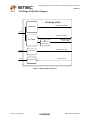
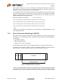
System Level Block Diagram . . . . . . . . . . . . . . . . . . . . . . . . . . . . . . . . . . . . . . . . . . . . . . . . . 11
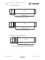
LAN9420/LAN9420i Internal Block Diagram . . . . . . . . . . . . . . . . . . . . . . . . . . . . . . . . . . . . . 11
LAN9420/LAN9420i 128-VTQFP (Top View). . . . . . . . . . . . . . . . . . . . . . . . . . . . . . . . . . . . . 15
PCI Bridge Block Diagram . . . . . . . . . . . . . . . . . . . . . . . . . . . . . . . . . . . . . . . . . . . . . . . . . . . 24
Device Operation . . . . . . . . . . . . . . . . . . . . . . . . . . . . . . . . . . . . . . . . . . . . . . . . . . . . . . . . . . 25
CSR Double Endian Mapping . . . . . . . . . . . . . . . . . . . . . . . . . . . . . . . . . . . . . . . . . . . . . . . . 27
I/O Bar Mapping . . . . . . . . . . . . . . . . . . . . . . . . . . . . . . . . . . . . . . . . . . . . . . . . . . . . . . . . . . . 27
Interrupt Generation . . . . . . . . . . . . . . . . . . . . . . . . . . . . . . . . . . . . . . . . . . . . . . . . . . . . . . . . 28
Interrupt Controller Block Diagram. . . . . . . . . . . . . . . . . . . . . . . . . . . . . . . . . . . . . . . . . . . . . 29
EEPROM Access Flow Diagram . . . . . . . . . . . . . . . . . . . . . . . . . . . . . . . . . . . . . . . . . . . . . . 33
EEPROM ERASE Cycle . . . . . . . . . . . . . . . . . . . . . . . . . . . . . . . . . . . . . . . . . . . . . . . . . . . . 34
EEPROM ERAL Cycle . . . . . . . . . . . . . . . . . . . . . . . . . . . . . . . . . . . . . . . . . . . . . . . . . . . . . . 34
EEPROM EWDS Cycle . . . . . . . . . . . . . . . . . . . . . . . . . . . . . . . . . . . . . . . . . . . . . . . . . . . . . 35
EEPROM EWEN Cycle . . . . . . . . . . . . . . . . . . . . . . . . . . . . . . . . . . . . . . . . . . . . . . . . . . . . . 35
EEPROM READ Cycle. . . . . . . . . . . . . . . . . . . . . . . . . . . . . . . . . . . . . . . . . . . . . . . . . . . . . . 36
EEPROM WRITE Cycle . . . . . . . . . . . . . . . . . . . . . . . . . . . . . . . . . . . . . . . . . . . . . . . . . . . . . 36
EEPROM WRAL Cycle . . . . . . . . . . . . . . . . . . . . . . . . . . . . . . . . . . . . . . . . . . . . . . . . . . . . . 37
Ring and Chain Descriptor Structures . . . . . . . . . . . . . . . . . . . . . . . . . . . . . . . . . . . . . . . . . . 40
Receive Descriptor. . . . . . . . . . . . . . . . . . . . . . . . . . . . . . . . . . . . . . . . . . . . . . . . . . . . . . . . . 41
Transmit Descriptor . . . . . . . . . . . . . . . . . . . . . . . . . . . . . . . . . . . . . . . . . . . . . . . . . . . . . . . . 45
VLAN Frame . . . . . . . . . . . . . . . . . . . . . . . . . . . . . . . . . . . . . . . . . . . . . . . . . . . . . . . . . . . . . 55
RXCOE Checksum Calculation . . . . . . . . . . . . . . . . . . . . . . . . . . . . . . . . . . . . . . . . . . . . . . . 60
Type II Ethernet Frame . . . . . . . . . . . . . . . . . . . . . . . . . . . . . . . . . . . . . . . . . . . . . . . . . . . . . 61
Ethernet Frame with VLAN Tag . . . . . . . . . . . . . . . . . . . . . . . . . . . . . . . . . . . . . . . . . . . . . . . 61
Ethernet Frame with Length Field and SNAP Header . . . . . . . . . . . . . . . . . . . . . . . . . . . . . . 61
Ethernet Frame with VLAN Tag and SNAP Header. . . . . . . . . . . . . . . . . . . . . . . . . . . . . . . . 62
Ethernet Frame with multiple VLAN Tags and SNAP Header . . . . . . . . . . . . . . . . . . . . . . . . 62
100BASE-TX Data Path. . . . . . . . . . . . . . . . . . . . . . . . . . . . . . . . . . . . . . . . . . . . . . . . . . . . . 65
Receive Data Path . . . . . . . . . . . . . . . . . . . . . . . . . . . . . . . . . . . . . . . . . . . . . . . . . . . . . . . . . 67
Direct Cable Connection vs. Cross-Over Cable Connection . . . . . . . . . . . . . . . . . . . . . . . . . 72
LAN9420/LAN9420i Device Power States . . . . . . . . . . . . . . . . . . . . . . . . . . . . . . . . . . . . . . . 75
Wake Event Detection Block Diagram . . . . . . . . . . . . . . . . . . . . . . . . . . . . . . . . . . . . . . . . . . 80
LAN9420/LAN9420i CSR Memory Map. . . . . . . . . . . . . . . . . . . . . . . . . . . . . . . . . . . . . . . . . 84
Example ADDRL, ADDRH Address Ordering . . . . . . . . . . . . . . . . . . . . . . . . . . . . . . . . . . . 124
Output Equivalent Test Load . . . . . . . . . . . . . . . . . . . . . . . . . . . . . . . . . . . . . . . . . . . . . . . . 161
PCI Clock Timing . . . . . . . . . . . . . . . . . . . . . . . . . . . . . . . . . . . . . . . . . . . . . . . . . . . . . . . . . 162
PCI I/O Timing . . . . . . . . . . . . . . . . . . . . . . . . . . . . . . . . . . . . . . . . . . . . . . . . . . . . . . . . . . . 163
EEPROM Timing . . . . . . . . . . . . . . . . . . . . . . . . . . . . . . . . . . . . . . . . . . . . . . . . . . . . . . . . . 165
LAN9420/LAN9420i 128-VTQFP Package Definition . . . . . . . . . . . . . . . . . . . . . . . . . . . . . 167
LAN9420/LAN9420i 128-VTQFP Recommended PCB Land Pattern . . . . . . . . . . . . . . . . . 168
Revision 1.22 (09-25-08)
8
DATASHEET
SMSC LAN9420/LAN9420i
Single-Chip Ethernet Controller with HP Auto-MDIX Support and PCI Interface
Datasheet
List of Tables
Table 2.1 PCI Bus Interface Pins. . . . . . . . . . . . . . . . . . . . . . . . . . . . . . . . . . . . . . . . . . . . . . . . . . . . . . . 16
Table 2.2 EEPROM . . . . . . . . . . . . . . . . . . . . . . . . . . . . . . . . . . . . . . . . . . . . . . . . . . . . . . . . . . . . . . . . . 17
Table 2.3 GPIO and LED Pins. . . . . . . . . . . . . . . . . . . . . . . . . . . . . . . . . . . . . . . . . . . . . . . . . . . . . . . . . 18
Table 2.4 Configuration Pins . . . . . . . . . . . . . . . . . . . . . . . . . . . . . . . . . . . . . . . . . . . . . . . . . . . . . . . . . . 18
Table 2.5 PLL and Ethernet PHY Pins . . . . . . . . . . . . . . . . . . . . . . . . . . . . . . . . . . . . . . . . . . . . . . . . . . 19
Table 2.6 Power and Ground Pins. . . . . . . . . . . . . . . . . . . . . . . . . . . . . . . . . . . . . . . . . . . . . . . . . . . . . . 20
Table 2.7 No-Connect Pins . . . . . . . . . . . . . . . . . . . . . . . . . . . . . . . . . . . . . . . . . . . . . . . . . . . . . . . . . . . 20
Table 2.8 128-VTQFP Package Pin Assignments. . . . . . . . . . . . . . . . . . . . . . . . . . . . . . . . . . . . . . . . . . 21
Table 3.1 PCI Address Spaces . . . . . . . . . . . . . . . . . . . . . . . . . . . . . . . . . . . . . . . . . . . . . . . . . . . . . . . . 26
Table 3.2 EEPROM Format. . . . . . . . . . . . . . . . . . . . . . . . . . . . . . . . . . . . . . . . . . . . . . . . . . . . . . . . . . . 31
Table 3.3 EEPROM Variable Defaults. . . . . . . . . . . . . . . . . . . . . . . . . . . . . . . . . . . . . . . . . . . . . . . . . . . 32
Table 3.4 Required EECLK Cycles . . . . . . . . . . . . . . . . . . . . . . . . . . . . . . . . . . . . . . . . . . . . . . . . . . . . . 37
Table 3.5 RDES0 Bit Fields . . . . . . . . . . . . . . . . . . . . . . . . . . . . . . . . . . . . . . . . . . . . . . . . . . . . . . . . . . . 41
Table 3.6 RDES1 Bit Fields . . . . . . . . . . . . . . . . . . . . . . . . . . . . . . . . . . . . . . . . . . . . . . . . . . . . . . . . . . . 44
Table 3.7 RDES2 Bit Fields . . . . . . . . . . . . . . . . . . . . . . . . . . . . . . . . . . . . . . . . . . . . . . . . . . . . . . . . . . . 44
Table 3.8 RDES3 Bit Fields . . . . . . . . . . . . . . . . . . . . . . . . . . . . . . . . . . . . . . . . . . . . . . . . . . . . . . . . . . . 45
Table 3.9 TDES0 Bit Fields . . . . . . . . . . . . . . . . . . . . . . . . . . . . . . . . . . . . . . . . . . . . . . . . . . . . . . . . . . . 46
Table 3.10 TDES1 Bit Fields . . . . . . . . . . . . . . . . . . . . . . . . . . . . . . . . . . . . . . . . . . . . . . . . . . . . . . . . . . . 47
Table 3.11 TDES2 Bit Fields . . . . . . . . . . . . . . . . . . . . . . . . . . . . . . . . . . . . . . . . . . . . . . . . . . . . . . . . . . . 49
Table 3.12 TDES3 Bit Fields . . . . . . . . . . . . . . . . . . . . . . . . . . . . . . . . . . . . . . . . . . . . . . . . . . . . . . . . . . . 49
Table 3.13 Address Filtering Modes . . . . . . . . . . . . . . . . . . . . . . . . . . . . . . . . . . . . . . . . . . . . . . . . . . . . . 55
Table 3.14 Wakeup Frame Filter Register Structure . . . . . . . . . . . . . . . . . . . . . . . . . . . . . . . . . . . . . . . . . 57
Table 3.15 Filter i Byte Mask Bit Definitions . . . . . . . . . . . . . . . . . . . . . . . . . . . . . . . . . . . . . . . . . . . . . . . 58
Table 3.16 Filter i Command Bit Definitions . . . . . . . . . . . . . . . . . . . . . . . . . . . . . . . . . . . . . . . . . . . . . . . 58
Table 3.17 Filter i Offset Bit Definitions . . . . . . . . . . . . . . . . . . . . . . . . . . . . . . . . . . . . . . . . . . . . . . . . . . . 58
Table 3.18 Filter i CRC-16 Bit Definitions . . . . . . . . . . . . . . . . . . . . . . . . . . . . . . . . . . . . . . . . . . . . . . . . . 59
Table 3.19 Wakeup Generation Cases . . . . . . . . . . . . . . . . . . . . . . . . . . . . . . . . . . . . . . . . . . . . . . . . . . . 59
Table 3.20 TX Checksum Preamble . . . . . . . . . . . . . . . . . . . . . . . . . . . . . . . . . . . . . . . . . . . . . . . . . . . . . 63
Table 3.21 4B/5B Code Table . . . . . . . . . . . . . . . . . . . . . . . . . . . . . . . . . . . . . . . . . . . . . . . . . . . . . . . . . . 65
Table 3.22 Reset Map . . . . . . . . . . . . . . . . . . . . . . . . . . . . . . . . . . . . . . . . . . . . . . . . . . . . . . . . . . . . . . . . 79
Table 3.23 PHY Resets . . . . . . . . . . . . . . . . . . . . . . . . . . . . . . . . . . . . . . . . . . . . . . . . . . . . . . . . . . . . . . . 80
Table 4.1 Register Bit Types . . . . . . . . . . . . . . . . . . . . . . . . . . . . . . . . . . . . . . . . . . . . . . . . . . . . . . . . . . 85
Table 4.2 System Control and Status Register Addresses . . . . . . . . . . . . . . . . . . . . . . . . . . . . . . . . . . . 86
Table 4.3 EEPROM Enable Bit Definitions . . . . . . . . . . . . . . . . . . . . . . . . . . . . . . . . . . . . . . . . . . . . . . . 93
Table 4.4 DMAC Control and Status Register (DCSR) Map . . . . . . . . . . . . . . . . . . . . . . . . . . . . . . . . . 103
Table 4.5 MAC Control and Status Register (MCSR) Map . . . . . . . . . . . . . . . . . . . . . . . . . . . . . . . . . . 118
Table 4.6 ADDRL, ADDRH Byte Ordering. . . . . . . . . . . . . . . . . . . . . . . . . . . . . . . . . . . . . . . . . . . . . . . 124
Table 4.7 PHY Control and Status Registers . . . . . . . . . . . . . . . . . . . . . . . . . . . . . . . . . . . . . . . . . . . . 135
Table 4.8 MODE Control . . . . . . . . . . . . . . . . . . . . . . . . . . . . . . . . . . . . . . . . . . . . . . . . . . . . . . . . . . . . 144
Table 4.9 PCI Configuration Space CSR (CONFIG CSR) Address Map . . . . . . . . . . . . . . . . . . . . . . . 149
Table 4.10 Standard PCI Header Registers Supported. . . . . . . . . . . . . . . . . . . . . . . . . . . . . . . . . . . . . . 150
Table 5.1 D0 - Normal Operation - Supply and Current (Typical) . . . . . . . . . . . . . . . . . . . . . . . . . . . . . 156
Table 5.2 D3 - Enabled for Wake Up Packet Detection - Supply and Current (Typical) . . . . . . . . . . . . 157
Table 5.3 D3 - Enabled for Link Status Change Detection - Supply and Current (Typical) . . . . . . . . . . 157
Table 5.4 D3 - PHY in General Power Down Mode - Supply and Current (Typical) . . . . . . . . . . . . . . . 158
Table 5.5 Maximum Power Consumption - Supply and Current (Maximum). . . . . . . . . . . . . . . . . . . . . 158
Table 5.6 I/O Buffer Characteristics. . . . . . . . . . . . . . . . . . . . . . . . . . . . . . . . . . . . . . . . . . . . . . . . . . . . 159
Table 5.7 100BASE-TX Transceiver Characteristics. . . . . . . . . . . . . . . . . . . . . . . . . . . . . . . . . . . . . . . 160
Table 5.8 10BASE-T Transceiver Characteristics . . . . . . . . . . . . . . . . . . . . . . . . . . . . . . . . . . . . . . . . . 160
Table 5.9 PCI Clock Timing Values . . . . . . . . . . . . . . . . . . . . . . . . . . . . . . . . . . . . . . . . . . . . . . . . . . . . 162
Table 5.10 PCI I/O Timing Measurement Conditions . . . . . . . . . . . . . . . . . . . . . . . . . . . . . . . . . . . . . . . 163
Table 5.11 PCI I/O Timing Values . . . . . . . . . . . . . . . . . . . . . . . . . . . . . . . . . . . . . . . . . . . . . . . . . . . . . . 164
Table 5.12 EEPROM Timing Values . . . . . . . . . . . . . . . . . . . . . . . . . . . . . . . . . . . . . . . . . . . . . . . . . . . . 165
SMSC LAN9420/LAN9420i
9
DATASHEET
Revision 1.22 (09-25-08)
Single-Chip Ethernet Controller with HP Auto-MDIX Support and PCI Interface
Datasheet
Table 5.13 LAN9420/LAN9420i Crystal Specifications . . . . . . . . . . . . . . . . . . . . . . . . . . . . . . . . . . . . . . 166
Table 6.1 LAN9420/LAN9420i 128-VTQFP Dimensions . . . . . . . . . . . . . . . . . . . . . . . . . . . . . . . . . . . . 168
Table 7.1 Customer Revision History . . . . . . . . . . . . . . . . . . . . . . . . . . . . . . . . . . . . . . . . . . . . . . . . . . 169
Revision 1.22 (09-25-08)
10
DATASHEET
SMSC LAN9420/LAN9420i
Single-Chip Ethernet Controller with HP Auto-MDIX Support and PCI Interface
Datasheet
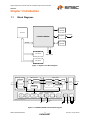
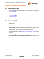
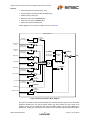
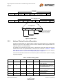
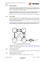
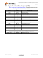
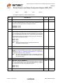
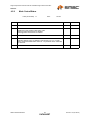
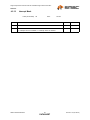
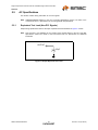
Chapter 1 Introduction
1.1
Block Diagrams
EEPROM
(optional)
PCI Host
To Ethernet
LAN9420/LAN9420i
Magnetics
GPIOs/LEDs
(optional)
PCI Bus
External
25MHz Crystal
PCI Device
PCI Device
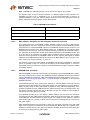
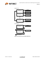
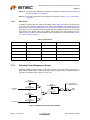
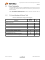
Figure 1.1 System Level Block Diagram
PCI Bridge (PCIB)
DMA Controller
PCI Master
Ethernet MAC
TX DMA Engine
TX FIFO (2KB)
TX COE
RX DMA Engine
RX FIFO (2KB)
RX COE
Arbiter
PCI
MAC
MAC Interface Layer
(MIL)
DMA Control &
Status Registers
(DCSR)
PCI Target
10/100
Ethernet
PHY
Ethernet
MAC Control & Status
Registers (MCSR)
System Control Block (SCB)
Interrupt
Controller
(INT)
Power
Management
(PM)
System Control &
Status Registers
(SCSR)
EEPROM
Controller
(EPC)
GPIO/LED
Controller
(GPIO )
GP Timer
Free-Run
Counter
3.3V to 1.8V
Regulator
PLL
LAN9420/LAN9420i
EEPROM
(optional)
GPIOs/LEDs
(optional)
+3.3V
25MHz
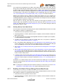
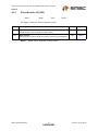
Figure 1.2 LAN9420/LAN9420i Internal Block Diagram
SMSC LAN9420/LAN9420i
11
DATASHEET
Revision 1.22 (09-25-08)
Single-Chip Ethernet Controller with HP Auto-MDIX Support and PCI Interface
Datasheet
1.2
General Description
LAN9420/LAN9420i is a full-featured, Fast Ethernet controller which allows for the easy and costeffective integration of Fast Ethernet into a PCI-based system. A system configuration diagram of
LAN9420/LAN9420i in a typical embedded environment can be seen in Figure 1.1, followed by an
internal block diagram of LAN9420/LAN9420i in Figure 1.2. LAN9420/LAN9420i consists of a PCI
Local Bus Specification Revision 3.0 compliant interface, DMA Controller, Ethernet MAC, and 10/100
Ethernet PHY.
LAN9420/LAN9420i provides full IEEE 802.3 compliance and all internal components support full/halfduplex 10BASE-T, 100BASE-TX, and manual full-duplex flow control. The descriptor based scattergather DMA supports usage of zero-copy drivers, effectively increasing throughput while decreasing
Host load. The integrated IRQ deassertion timer allows a minimum IRQ deassertion time to be set,
providing reduced Host load and greater control over service routines. Automatic 32-bit CRC
generation/checking, automatic payload padding, and 2K jumbo packets (2048 byte) are supported.
Big, little, and mixed endian support provides independent control over register, descriptor, and buffer
endianess. This feature enables easy integration into various ARM/MIPS/PowerPC designs.
LAN9420/LAN9420i supports the PCI Bus Power Management Interface Specification Revision 1.1 and
provides the optional ability to generate wake events in the D3cold state when Vaux is available. Wake
on LAN, wake on link status change (energy detect), and magic packet wakeup detection are also
supported, allowing for a range of power management options.
LAN9420/LAN9420i contains an EEPROM controller for connection to an optional EEPROM. This
allows for the automatic loading of static configuration data upon power-up or reset. When connected,
the EEPROM can be configured to load a predetermined MAC address, the PCI SSID, and the PCI
SSVID of LAN9420/LAN9420i.
In addition to the primary functionality described above, LAN9420/LAN9420i provides additional
features designed for extended functionality. These include a multipurpose 16-bit configurable General
Purpose Timer (GPT), a Free-Run Counter, a 3-pin configurable GPIO/LED interface, and 2 GPO pins.
All aspects of LAN9420/LAN9420i are managed via a set of memory mapped control and status
registers.
LAN9420/LAN9420i’s performance and features make it an ideal solution for many applications in the
consumer electronics, enterprise, and industrial automation markets. Targeted applications include: set
top boxes (cable, satellite and IP), digital televisions, digital video recorders, home gateways, digital
media clients/servers, industrial automation systems, industrial single board PCs, and kiosk/POS
enterprise equipment.
Revision 1.22 (09-25-08)
12
DATASHEET
SMSC LAN9420/LAN9420i
Single-Chip Ethernet Controller with HP Auto-MDIX Support and PCI Interface
Datasheet
1.3
PCI Bridge
LAN9420/LAN9420i implements a PCI Local Bus Specification Revision 3.0 compliant interface,
supporting the PCI Bus Power Management Interface Specification Revision 1.1. It provides the PCI
Configuration Space Control and Status registers used to configure LAN9420/LAN9420i for PCI device
operation. Please refer to Section 3.2, "PCI Bridge (PCIB)," on page 23 for more information.
1.4
DMA Controller
The DMA controller consists of independent Transmit and Receive engines and a control and status
register (CSR) space. The Transmit Engine transfers data from Host memory to the MAC Interface
Layer (MIL) while the Receive Engine transfers data from the MIL to Host memory. The controller
utilizes descriptors to efficiently move data from source to destination with minimal processor
intervention. Descriptors are DWORD aligned data structures in system memory that inform the DMA
controller of the location of data buffers in Host memory and also provide a mechanism for
communicating the status to the Host CPU. The DMA controller has been designed for packet-oriented
data transfer, such as frames in Ethernet. Zero copy DMA transfer is supported. Copy operations for
the purpose of data re-alignment are not required in the case where buffers are fragmented or not
aligned to a DWORD boundary. The controller can be programmed to interrupt the Host on the
occurrence of particular events, such as frame transmit or receive transfer completed, and other
normal, as well as error, conditions. Please refer to Section 3.4, "DMA Controller (DMAC)," on page 38
for more information.
1.5
Ethernet MAC
The transmit and receive data paths are separate within the 10/100 Ethernet MAC, allowing the highest
performance, especially in full duplex mode. The data paths connect to the PCI Bridge via a DMA
engine. The MAC also implements a CSR space used by the Host to obtain status and control its
operation. The MAC Interface Layer (MIL), within the MAC, contains a 2K Byte transmit and receive
FIFO. The MIL supports store and forward and operate on second frame mode for minimum interpacket gap. Please refer to Section 3.5, "10/100 Ethernet MAC," on page 53 for more information.
1.6
Ethernet PHY
The PHY implements an IEEE 802.3 physical layer for twisted pair Ethernet applications. It can be
configured for either 100 Mbps (100BASE-TX) or 10 Mbps (10BASE-T) Ethernet operation in either full
or half duplex configurations. The PHY block includes support for auto-negotiation, auto-polarity
correction and Auto-MDIX. Minimal external components are required for the utilization of the
integrated PHY. Please refer to Section 3.6, "10/100 Ethernet PHY," on page 64 for more information.
1.7
System Control Block
The System Control Block provides the following additional elements for system operation. These
elements are controlled via its System Control and Status Registers (SCSR). Please refer to Section
3.3, "System Control Block (SCB)," on page 28 for more information.
1.7.1
Interrupt Controller
The Interrupt Controller (INT) can be programmed to issue a PCI interrupt to the Host on the
occurrence of various events. Please refer to Section 3.3.1, "Interrupt Controller," on page 28 for more
information.
SMSC LAN9420/LAN9420i
13
DATASHEET
Revision 1.22 (09-25-08)
Single-Chip Ethernet Controller with HP Auto-MDIX Support and PCI Interface
Datasheet
1.7.2
PLL and Power Management
LAN9420/LAN9420i interfaces with a 25MHz crystal oscillator from which all internal clocks, with the
exception of PCI clock, are generated. The internal clocks are all generated by the PLL and Power
Management blocks. Various power savings modes exists that allow for the clocks to be shut down.
These modes are defined by the power state of the PCI function. Please refer to Section 3.7, "Power
Management," on page 73 for more information.
1.7.3
EEPROM Controller
LAN9420/LAN9420i provides support for an optional EEPROM via the EEPROM Controller. Please
refer to Section 3.3.5, "EEPROM Controller (EPC)," on page 31 for more information.
1.7.4
GPIO/LED Controller
The 3-bit GPIO and 2-bit GPO (Multiplexed on the LED and EEPROM Pins) interface is managed by
the GPIO/LED Controller. It is accessible via the System Control and Status Registers (SCSR). The
GPIO signals can function as inputs, push-pull outputs and open drain outputs. The GPIOs can also
be configured to trigger interrupts with programmable polarity. The GPOs are outputs only and have
no means of generating interrupts.
Please refer to Section 4.2.5, "General Purpose Input/Output Configuration Register (GPIO_CFG)," on
page 92 for more information.
1.7.5
General Purpose Timer
The General Purpose Timer has no dedicated function within LAN9420/LAN9420i and may be
programmed to issue a timed interrupt. Please refer to Section 3.3.3, "General Purpose Timer (GPT),"
on page 30 for more information.
1.7.6
Free Run Counter
The Free Run Counter has no dedicated function within LAN9420/LAN9420i and may be used by the
software drivers as a timebase. Please refer to Section 3.3.4, "Free-Run Counter (FRC)," on page 31
for more information.
1.8
Control and Status Registers (CSR)
LAN9420/LAN9420i’s functions are controlled and monitored by the Host via the Control and Status
Registers (CSR). This register space includes registers that control and monitor the DMA controller
(DMA Control and Status Registers - DCSR), the MAC (MAC Control and Status Registers - MCSR),
the PHY (accessed indirectly through the MAC via the MII_ACCESS and MII_DATA registers), and the
elements of the System Control Block via the System Control and Status Registers (SCSR). The CSR
may be accessed be via I/O or memory operations. Big or Little Endian access is also configurable.
Revision 1.22 (09-25-08)
14
DATASHEET
SMSC LAN9420/LAN9420i
Single-Chip Ethernet Controller with HP Auto-MDIX Support and PCI Interface
Datasheet
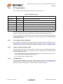
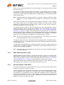
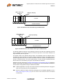
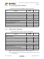
NC
EECLK/GPO4
EECS
NC
EEDIO/GPO3
NC
VDD33IO
VSS
AD0
AD1
AD2
AD3
AD4
VSS
VDD18CORE
VDD33IO
VSS
AD5
AD6
AD7
nCBE0
AD8
VDD33IO
VSS
AD9
AD10
AD11
AD12
AD13
VDD33IO
VSS
AD14
95
94
93
92
91
90
89
88
87
86
85
84
83
82
81
80
79
78
77
76
75
74
73
72
71
70
69
68
67
66
65
TOP VIEW
17
18
19
20
21
22
23
24
25
26
27
28
29
30
31
32
nGNT
nREQ
nPME
VSS
VDD33IO
AD31
AD30
AD29
AD28
AD27
VSS
VDD33IO
AD26
AD25
AD24
NC
15
PCInRST
16
14
nINT
PCICLK
13
VDD33IO
9
VDD18CORE
12
8
VDD18CORE
VSS
7
VDD33IO
11
6
VDD33IO
VSS
5
VDD33IO
10
4
VSS
VSS
3
34
33
VDD33IO
NC
AUTOMDIX_EN
VDD18TX
VDD18PLL
VSS
XO
XI
PWRGOOD
VAUXDET
GPIO0/nLED1
NC
NC
NC
NC
NC
SMSC
LAN9420/LAN9420i
128-VTQFP
2
VSS
VDD33BIAS
NC
NC
102
103
104
105
106
107
108
109
110
111
112
113
114
115
116
117
118
119
120
121
122
123
124
125
126
127
128
1
TPOTPO+
VSS
VDD33A
TPINC
TPI+
VDD33A
VSS
EXRES
64
63
62
61
60
59
58
57
56
55
54
53
52
51
50
49
48
47
46
45
44
43
42
41
40
39
38
37
36
35
97
98
99
100
101
GPIO2/nLED3
NC
VSS
GPIO1/nLED2
NC
96
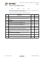
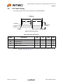
Chapter 2 Pin Description and Configuration
NC
NC
AD15
nCBE1
PAR
nSERR
VDD33IO
VSS
nPERR
nSTOP
nDEVSEL
nTRDY
nIRDY
VDD33IO
VSS
VSS
nFRAME
nCBE2
AD16
AD17
AD18
VDD33IO
VSS
AD19
AD20
AD21
AD22
AD23
VDD33IO
VSS
IDSEL
nCBE3
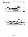
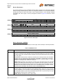
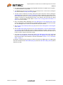
NOTE: When HP Auto-MDIX is activated, the TPO+/- pins function as TPI+/- and vice-versa.
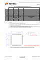
Figure 2.1 LAN9420/LAN9420i 128-VTQFP (Top View)
SMSC LAN9420/LAN9420i
15
DATASHEET
Revision 1.22 (09-25-08)
Single-Chip Ethernet Controller with HP Auto-MDIX Support and PCI Interface
Datasheet
2.1
Pin List
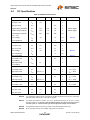
Table 2.1 PCI Bus Interface Pins
NUM
PINS
NAME
SYMBOL
1
1
PCI Clock In
PCI Frame
PCICLK
nFRAME
32
PCI Address
and Data Bus
PCI Reset
PCI Bus
Command and
Byte Enables
PCI Initiator
Ready
PCI Target
Ready
PCI Stop
AD[31:0]
1
4
1
PCInRST
nCBE[3:0]
DESCRIPTION
IS
IPCI/
OPCI
IPCI/
OPCI
IS
IPCI/
OPCI
PCI Clock In: 0 to 33MHz PCI Clock Input.
PCI Cycle Frame
PCI Initiator Ready
PCI Address and Data Bus
PCI Reset
PCI Bus Command and Byte Enables
PCI Device
Select
PCI Parity
nDEVSEL
nPERR
1
PCI Parity
Error
PCI System
Error
PCI Interrupt
nINT
IPCI/
OPCI
IPCI/
OPCI
IPCI/
OPCI
IPCI/
OPCI
IPCI/
OPCI
IPCI/
OPCI
IPCI/
OPCI
OPCI
1
1
PCI IDSEL
PCI Request
IDSEL
nREQ
IPCI
OPCI
Note:
This pin is an open drain output.
PCI IDSEL
PCI Request
IPCI
OPCI
Note:
This pin is a tri-state output.
PCI Grant
PCI Power Management Event
1
1
1
1
1
1
1
1
1
PCI Grant
PCI Power
Management
Event
Power Good
nIRDY
BUFFER
TYPE
nTRDY
nSTOP
PAR
nSERR
nGNT
nPME
PCI Target Ready
PCI Stop
PCI Device Select
PCI Parity
PCI Parity Error
PCI System Error
PCI Interrupt
Note:
PWRGOOD
IS
(PD)
This pin is an open drain output.
PCI Bus Power Good: This pin is used to sense the
presence of PCI bus power during the D3 power
management state.
Note:
1
VAUX Detection
VAUXDET
IS
(PD)
This pin is pulled low through an internal pulldown resistor
PCI Auxiliary Voltage Sense: This pin is used to sense
the presence of a 3.3V auxiliary supply in order to define
the PME support available.
Note:
Revision 1.22 (09-25-08)
16
DATASHEET
This pin is pulled low through an internal pulldown resistor
SMSC LAN9420/LAN9420i
Single-Chip Ethernet Controller with HP Auto-MDIX Support and PCI Interface
Datasheet
Table 2.2 EEPROM
NUM
PINS
1
1
1
NAME
SYMBOL
BUFFER
TYPE
EEPROM Data
EEDIO
IS/O8
GPO3
GPO3
O8
TX_EN
TX_EN
O8
TX_CLK
TX_CLK
O8
EEPROM Chip
Select
EEPROM
Clock
EECS
O8
EECLK
GPO4
GPO4
IS/O8
(PU)
Note 2.1
O8
RX_DV
RX_DV
O8
RX_CLK
RX_CLK
O8
Note 2.1
SMSC LAN9420/LAN9420i
DESCRIPTION
EEPROM Data: This bi-directional pin can be connected
to an optional serial EEPROM DIO.
General Purpose Output 3: This pin can also function
as a general purpose output. The EECS pin is deasserted
so as to never unintentionally access the serial EEPROM.
TX_EN Signal Monitor: This pin can also be configured
to monitor the TX_EN signal on the internal MII port. The
EECS pin is deasserted so as to never unintentionally
access the serial EEPROM.
TX_CLK Signal Monitor: This pin can also be configured
to monitor the TX_CLK signal on the internal MII port.
The EECS pin is deasserted so as to never
unintentionally access the serial EEPROM.
Serial EEPROM Chip Select.
EEPROM Clock: Serial EEPROM Clock pin
General Purpose Output 4: This pin can also function
as a general purpose output. The EECS pin is deasserted
so as to never unintentionally access the serial EEPROM.
RX_DV Signal Monitor: This pin can also be configured
to monitor the RX_DV signal on the internal MII port. The
EECS pin is deasserted so as to never unintentionally
access the serial EEPROM.
RX_CLK Signal Monitor: This pin can also be
configured to monitor the RX_CLK signal on the internal
MII port. The EECS pin is deasserted so as to never
unintentionally access the serial EEPROM.
This pin is used for factory testing and is latched on power up. This pin is pulled high
through an internal resistor and must not be pulled low externally. This pin must be
augmented with an external resistor when connected to a load. The value of the resistor
must be such that the pin reaches its valid level before de-assertion of PCInRST following
power up. The “IS” input buffer type is enabled only during power up. The “IS” input buffer
type is disabled at all other times.
17
DATASHEET
Revision 1.22 (09-25-08)
Single-Chip Ethernet Controller with HP Auto-MDIX Support and PCI Interface
Datasheet
Table 2.3 GPIO and LED Pins
NUM
PINS
1
1
BUFFER
TYPE
NAME
SYMBOL
General
Purpose I/O
data 0
GPIO0
IS/O12/
OD12
nLED1 (Speed
Indicator)
nLED1
OD12
General
Purpose I/O
data 1
GPIO1
IS/O12/
OD12
nLED2 (Link &
Activity
Indicator)
nLED2
OD12
General
Purpose I/O
data 2
GPIO2
IS/O12/
OD12
nLED3 (FullDuplex
Indicator)
nLED3
OD12
1
DESCRIPTION
General Purpose I/O data 0: This general-purpose pin is
fully programmable as either push-pull output, open-drain
output or input by writing the GPIO_CFG configuration
register in the SCSR. GPIO pins are Schmitt-triggered
inputs.
nLED1 (Speed Indicator): This pin can also function as
the Ethernet speed indicator LED and is driven low when
the operating speed is 100Mbs, during auto-negotiation,
and when the cable is disconnected. This pin is driven
high only during 10Mbs operation.
General Purpose I/O data 1: This general-purpose pin is
fully programmable as either push-pull output, open-drain
output or input by writing the GPIO_CFG configuration
register in the SCSR. GPIO pins are Schmitt-triggered
inputs.
nLED2 (Link & Activity Indicator): This pin can also
function as the Ethernet Link and Activity Indicator LED
and is driven low (LED on) when LAN9420/LAN9420i
detects a valid link. This pin is pulsed high (LED off) for
80mS whenever transmit or receive activity is detected.
This pin is then driven low again for a minimum of 80mS,
after which time it will repeat the process if TX or RX
activity is detected. Effectively, LED2 is activated solid for
a link. When transmit or receive activity is sensed, LED2
will flash as an activity indicator.
General Purpose I/O data 2: This general-purpose pin is
fully programmable as either push-pull output, open-drain
output or input by writing the GPIO_CFG configuration
register in the SCSR. GPIO pins are Schmitt-triggered
inputs.
nLED3 (Full-Duplex Indicator): This pin can also
function as the Ethernet Full-Duplex Indicator LED and is
driven low when the link is operating in full-duplex mode.
Table 2.4 Configuration Pins
NUM
PINS
NAME
SYMBOL
AutoMDIX
Enable
AUTOMDIX_EN
1
Revision 1.22 (09-25-08)
BUFFER
TYPE
IS
(PU)
DESCRIPTION
AutoMDIX Enable: Enables Auto-MDIX. Pull high or
leave unconnected to enable Auto-MDIX, pull low to
disable Auto-MDIX.
18
DATASHEET
SMSC LAN9420/LAN9420i
Single-Chip Ethernet Controller with HP Auto-MDIX Support and PCI Interface
Datasheet
Table 2.5 PLL and Ethernet PHY Pins
NUM
PINS
NAME
SYMBOL
BUFFER
TYPE
Crystal Input
XI
ICLK
Crystal Input: External 25MHz crystal input. This pin
can also be driven by a single-ended clock oscillator.
When this method is used, XO should be left
unconnected.
1
Crystal
Output
XO
OCLK
Crystal Output: External 25MHz crystal output.
Ethernet TX
Data Out
Negative
TPO-
AIO
1
Ethernet Transmit Data Out Negative: The transmit
data outputs may be swapped internally with receive
data inputs when Auto-MDIX is enabled.
Ethernet TX
Data Out
Positive
TPO+
AIO
1
Ethernet Transmit Data Out Positive: The transmit
data outputs may be swapped internally with receive
data inputs when Auto-MDIX is enabled.
Ethernet RX
Data In
Negative
TPI-
AIO
1
Ethernet Receive Data In Negative: The receive data
inputs may be swapped internally with transmit data
outputs when Auto-MDIX is enabled.
Ethernet RX
Data In
Positive
TPI+
AIO
1
Ethernet Receive Data In Positive: The receive data
inputs may be swapped internally with transmit data
outputs when Auto-MDIX is enabled.
External
PHY Bias
Resistor
EXRES
AI
1
External PHY Bias Resistor: Used for the internal
PHY bias circuits. Connect to an external 12.4K 1.0%
resistor to ground.
1
SMSC LAN9420/LAN9420i
DESCRIPTION
19
DATASHEET
Revision 1.22 (09-25-08)
Single-Chip Ethernet Controller with HP Auto-MDIX Support and PCI Interface
Datasheet
Table 2.6 Power and Ground Pins
NUM
PINS
2
1
1
1
15
NAME
SYMBOL
BUFFER
TYPE
+3.3V
Analog
Power
Supply
VDD33A
P
+1.8V PLL
Power
Supply
VDD18PLL
+1.8V TX
Power
Supply
VDD18TX
+3.3V
Master Bias
Power
Supply
VDD33BIAS
+3.3V I/O
Power
VDD33IO
DESCRIPTION
+3.3V Analog Power Supply
Refer to the LAN9420/LAN9420i application note for
connection information.
P
+1.8V PLL Power Supply: This pin must be connected
to VDD18CORE for proper operation.
Refer to the LAN9420/LAN9420i application note for
additional connection information.
P
+1.8V Transmitter Power Supply: This pin must be
connected to VDD18CORE for proper operation.
Refer to the LAN9420/LAN9420i application note for
additional connection information.
P
+3.3V Master Bias Power Supply
Refer to the LAN9420/LAN9420i application note for
additional connection information.
P
+3.3V Power Supply for I/O Pins and Internal
Regulator
Refer to the LAN9420/LAN9420i application note for
additional connection information.
21
Ground
VSS
P
Common Ground for I/O Pins, Core, and Analog
Circuitry
VDD18CORE
P
3
+1.8V Core
Power
Digital Core +1.8V Power Supply Output from
Internal Regulator
Refer to the LAN9420/LAN9420i application note for
additional connection information.
Table 2.7 No-Connect Pins
NUM
PINS
NAME
SYMBOL
BUFFER
TYPE
17
No Connect
NC
-
Revision 1.22 (09-25-08)
DESCRIPTION
No Connect: These pins must be left floating for
normal device operation.
20
DATASHEET
SMSC LAN9420/LAN9420i
Single-Chip Ethernet Controller with HP Auto-MDIX Support and PCI Interface
Datasheet
Table 2.8 128-VTQFP Package Pin Assignments
PIN
NUM
PIN NAME
PIN
NUM
PIN NAME
PIN
NUM
PIN NAME
PIN
NUM
PIN NAME
1
GPIO1/nLED2
33
nCBE3
65
AD14
97
NC
2
GPIO2/nLED3
34
IDSEL
66
VSS
98
NC
3
VDD33IO
35
VSS
67
VDD33IO
99
VSS
4
VSS
36
VDD33IO
68
AD13
100
TPO-
5
VDD33IO
37
AD23
69
AD12
101
TPO+
6
VDD33IO
38
AD22
70
AD11
102
VSS
7
VDD33IO
39
AD21
71
AD10
103
VDD33A
8
VDD18CORE
40
AD20
72
AD9
104
TPI-
9
VDD18CORE
41
AD19
73
VSS
105
NC
10
VSS
42
VSS
74
VDD33IO
106
TPI+
11
VSS
43
VDD33IO
75
AD8
107
VDD33A
12
VSS
44
AD18
76
nCBE0
108
VSS
13
VDD33IO
45
AD17
77
AD7
109
EXRES
14
nINT
46
AD16
78
AD6
110
VSS
15
PCInRST
47
nCBE2
79
AD5
111
VDD33BIAS
16
PCICLK
48
nFRAME
80
VSS
112
NC
17
nGNT
49
VSS
81
VDD33IO
113
NC
18
nREQ
50
VSS
82
VDD18CORE
114
NC
19
nPME
51
VDD33IO
83
VSS
115
AUTOMDIX_EN
20
VSS
52
nIRDY
84
AD4
116
VDD18TX
21
VDD33IO
53
nTRDY
85
AD3
117
VDD18PLL
22
AD31
54
nDEVSEL
86
AD2
118
VSS
23
AD30
55
nSTOP
87
AD1
119
XO
24
AD29
56
nPERR
88
AD0
120
XI
25
AD28
57
VSS
89
VSS
121
PWRGOOD
26
AD27
58
VDD33IO
90
VDD33IO
122
VAUXDET
27
VSS
59
nSERR
91
NC
123
GPIO0/nLED1
28
VDD33IO
60
PAR
92
EEDIO/GPO3
124
NC
29
AD26
61
nCBE1
93
NC
125
NC
30
AD25
62
AD15
94
EECS
126
NC
31
AD24
63
NC
95
EECLK/GPO4
127
NC
32
NC
64
NC
96
NC
128
NC
SMSC LAN9420/LAN9420i
21
DATASHEET
Revision 1.22 (09-25-08)
Single-Chip Ethernet Controller with HP Auto-MDIX Support and PCI Interface
Datasheet
2.2
Buffer Types
BUFFER TYPE
DESCRIPTION
IS
Schmitt-triggered Input
O8
Output with 8mA sink and 8mA source current
O12
Output with 12mA sink and 12mA source current
OD12
Open-drain output with 12mA sink current
IPCI
PCI compliant Input
OPCI
PCI compliant Output
PU
50uA (typical) internal pull-up. Unless otherwise noted in the pin description, internal pull-ups
are always enabled.
Note:
PD
50uA (typical) internal pull-down. Unless otherwise noted in the pin description, internal pulldowns are always enabled.
Note:
AI
Internal pull-up resistors prevent unconnected inputs from floating. Do not rely on
internal resistors to drive signals external to LAN9420/LAN9420i. When connected
to a load that must be pulled high, an external resistor must be added.
Internal pull-down resistors prevent unconnected inputs from floating. Do not rely
on internal resistors to drive signals external to LAN9420/LAN9420i. When
connected to a load that must be pulled low, an external resistor must be added.
Analog Input
AIO
Analog bi-directional
ICLK
Crystal oscillator input
OCLK
Crystal oscillator output
P
Power and Ground pin
Revision 1.22 (09-25-08)
22
DATASHEET
SMSC LAN9420/LAN9420i
Single-Chip Ethernet Controller with HP Auto-MDIX Support and PCI Interface
Datasheet
Chapter 3 Functional Description
3.1
Functional Overview
The LAN9420/LAN9420i Ethernet Controller consists of five major functional blocks. These blocks are:
PCI Bridge (PCIB)
System Control Block (SCB)
DMA Controller (DMAC)
10/100 Ethernet MAC
10/100 Ethernet PHY
The following sections discuss the features of each block. A block diagram of LAN9420/LAN9420i is
shown in Figure 1.2 LAN9420/LAN9420i Internal Block Diagram on page 11.
3.2
PCI Bridge (PCIB)
The PCI Bridge (PCIB) facilitates LAN9420/LAN9420i’s operation on a PCI bus as a device. It has the
following features:
PCI Master Interface: This interface connects LAN9420/LAN9420i to the PCI bus when it is
functioning as a PCI Master. It is used by the DMA engines to directly access the PCI Host’s memory.
PCI Target Interface: This interface connects LAN9420/LAN9420i to the PCI bus when it is functioning
as a PCI Target. It provides access to PCI Configuration Space Control and Status Register (CONFIG
CSR), and access to the Control and Status Registers (CSR) via I/O or Non-Prefetchable (NP) memory
accesses. In addition, Big/Little Endian support for the registers may be selected.
PCI Power Management Support: LAN9420/LAN9420i supports PCI Bus Power Management
Interface Specification Rev. 1.1. Refer to Section 3.7, "Power Management," on page 73 for more
information.
Interrupt Gating Logic: This logic controls assertion of the nINT signal to the Host system.
PCI Configuration Space Control and Status Registers (CONFIG CSR): The Host system controls
and monitors the LAN9420/LAN9420i device using registers in this space.
SMSC LAN9420/LAN9420i
23
DATASHEET
Revision 1.22 (09-25-08)
Single-Chip Ethernet Controller with HP Auto-MDIX Support and PCI Interface
Datasheet
3.2.1
PCI Bridge (PCIB) Block Diagram
PCI Bridge (PCIB)
To/From DMAC Arbiter
PCI Master
PCI
To/From CSR Blocks
PCI Target
nPME
nINT
PM Related Signals
(To/From PM)
PCI
Configuration
Space CSR
PM Signal (From PM)
PME Gating
IRQ (From INT)
Interrupt Gating
Figure 3.1 PCI Bridge Block Diagram
Revision 1.22 (09-25-08)
24
DATASHEET
SMSC LAN9420/LAN9420i
Single-Chip Ethernet Controller with HP Auto-MDIX Support and PCI Interface
Datasheet
3.2.2
PCI Interface Environments
The PCIB supports only Device operation. It functions as a simple bridge, permitting
LAN9420/LAN9420i to act as a master/target PCI device on the PCI bus. The Host performs PCI
arbitration and is responsible for initializing configuration space for all devices on the bus. Figure 3.2
illustrates Device operation.
Host
System
PCI
Bus
PCIB
PCI
Component
PCI
Component
LAN9420
PCI
Component
Figure 3.2 Device Operation
3.2.3
PCI Master Interface
The PCI Master Interface is used by the DMA engines to directly access the PCI Host’s memory. It is
used by the TX and RX DMA Controllers to access Host descriptor ring elements and Host DMA
buffers. No address translation occurs, as these entities are contained within the Host, which allocates
them within the flat PCI address space.
3.2.3.1
PCI Master Transaction Errors
In the event of an error during a descriptor read or during a transmit data read, the DMA controller will
generate a Master Bus Error Interrupt (MBERR_INT).
When an MBERR_INT is asserted, all subsequent transactions from the DMAC will be aborted. In
order to cleanly recover from this condition, a software reset or H/W reset must be performed. A
software reset is accomplished by setting the SRST bit of the BUS_MODE register.
Note: It is guaranteed that the MBERR_INT will be reported on the frame upon which the error
occurred as follows:
- Errors on descriptor reads will be aborted immediately.
- Errors on TX data will be reported either upon the data or the close descriptor (if the error
occurs on the last data transfer).
- DMA RX data and descriptor write operations are posted and will therefore not generate the
MBERR_INT.
SMSC LAN9420/LAN9420i
25
DATASHEET
Revision 1.22 (09-25-08)
Single-Chip Ethernet Controller with HP Auto-MDIX Support and PCI Interface
Datasheet
3.2.4
PCI Target Interface
The PCI target interface implements the address spaces listed in Table 3.1.
Table 3.1 PCI Address Spaces
SPACE
SIZE
Configuration
256 bytes
BAR0...BAR2
RESOURCE
PCI standard and PCIB-specific registers
RESERVED
BAR3
1 KB
Control and Status Registers (Non-prefetchable area)
BAR4
256B
Control and Status Registers (I/O area)
BAR5
RESERVED
Expansion ROM
-
RESERVED
The PCI Configuration space is used to identify PCI Devices, configure memory ranges, and manage
interrupts. The Host initializes and configures the PCI Device during a plug-and-play process.
The PCI Target Interface supports 32-bit slave accesses only. Non 32-bit PCI target reads to
LAN9420/LAN9420i will result in a full 32-bit read. Non 32-bit PCI target writes to LAN9420/LAN9420i
will be silently discarded.
3.2.4.1
PCI Configuration Space Registers
PCI Configuration Space Registers include the standard PCI header registers and PCIB extensions to
implement power management control/status registers. See Section 4.6, "PCI Configuration Space
CSR (CONFIG CSR)," on page 149 for further details. These registers exist in the configuration space.
3.2.4.2
Control and Status Registers (CSR)
The PCI Target Interface allows PCI bus masters to directly access the LAN9420/LAN9420i Control
and Status registers via memory or I/O operations. Each set of operations has an associated address
range that defines it as follows:
3.2.4.2.1
The non-prefetchable (NP) address range is mapped in BAR3. No data prefetch is performed when
serving PCI transactions targeting this address range.
The I/O address range is mapped in BAR4.
CSR ENDIANNESS
The Non-Prefetchable address range contains a double mapping of the CSR. These mappings allow
the registers to be accessed in little endian or big endian order. Figure 3.3, "CSR Double Endian
Mapping" illustrates the mapping. BA is the base address, as specified by BAR3.
Revision 1.22 (09-25-08)
26
DATASHEET
SMSC LAN9420/LAN9420i
Single-Chip Ethernet Controller with HP Auto-MDIX Support and PCI Interface
Datasheet
.
BA + 3FCh
CSR - Big Endian (512 Bytes)
BA + 200h
BA + 1FCh
CSR - Little Endian (512 Bytes)
BA (BAR3)
Figure 3.3 CSR Double Endian Mapping
3.2.4.2.2
I/O MAPPING OF CSR
The I/O BAR (BAR4) is double mapped over the CSR space with the non-prefetchable area. The CSR
big endian space is disabled, as the Host processors (Intel x86) that use the I/O BAR are little endian.
Note: A comparison of Figure 3.3 with Figure 3.4 indicates only the first 256 bytes of CSR little endian
space is addressable via the I/O BAR.
.
BA + 0FCh
CSR - Little Endian ( 256 Bytes)
I/O BAR and nonprefetchable memory
are double mapped to
the CSR space
BA (BAR4)
Figure 3.4 I/O Bar Mapping
3.2.4.3
PCI Target Interface Transaction Errors
If the Host system attempts an unsupported cycle type when accessing the CSR via the PCI Target
Interface, a slave transaction error will result and the PCI Target Interface will generate a Slave Bus
Error Interrupt (SBERR_INT), if enabled. CSR may only be read or written as DWORD quantities and
any other type of access is unsupported and will result in the assertion of SBERR_INT. Non-DWORD
reads will return a DWORD while non-DWORD writes are silently discarded. In order to cleanly recover
from this condition, a software reset or H/W reset must be performed. A software reset is accomplished
by setting the SRST bit of the BUS_MODE register.
3.2.4.4
PCI Discard Timer
When the PCI master performs a read of LAN9420/LAN9420i, the PCI Bridge will fetch the data and
acknowledge the PCI transfer when data is available. If the PCI master malfunctions and does
complete the transaction within 32768 PCI clocks, LAN9420/LAN9420i will flush the data to prevent a
potential bus lock-up.
3.2.5
Interrupt Gating Logic
One set of interrupts exists: PCI Host interrupts (PCI interrupts from LAN9420/LAN9420i to the PCI
Host). PCI Host interrupts result from the assertion of the internal IRQ signal from the Interrupt
Controller. Refer to Section 3.3.1, "Interrupt Controller," on page 28 for sources of this interrupt.
Figure 3.5 illustrates how interrupts are sourced by the Interrupt Controller to the PCIB and are
propagated to the Host. The Interrupt is passed on to the Host only when the Host has enabled it by
setting bit 10 in the PCI Device Command Register. The Host may obtain interrupt status by reading
SMSC LAN9420/LAN9420i
27
DATASHEET
Revision 1.22 (09-25-08)
Single-Chip Ethernet Controller with HP Auto-MDIX Support and PCI Interface
Datasheet
Bit 3 of the PCI Device Status Register. The PCI Device Status Register and PCI Device Command
Register are standard registers in PCI Configuration Space. Please refer to Section 4.6, "PCI
Configuration Space CSR (CONFIG CSR)," on page 149 for details.
PCIB
Interrupt
Controller
Bit 3
PCI Device
Status Register
IRQ
nINT
RW
(To Host)
Bit 10
PCI Device
Command Register
Figure 3.5 Interrupt Generation
3.3
System Control Block (SCB)
The System Control Block includes an interrupt controller, wake detection logic, a general-purpose
timer, a free-run counter and system control and status registers.
Interrupt Controller: The interrupt controller can be programmed to interrupt the Host system
applications on the occurrence of various events. The interrupt is routed to the Host system via the
PCIB.
Wake Detection Logic: This logic detects the occurrence of an enabled wake event and asserts the
PCI nPME signal, if enabled.
General Purpose Timer (GPT): The general purpose timer can be configured to generate a system
interrupt upon timeout.
Free-Run Counter (FRC): A 32-bit free-running counter with a 160 ns resolution.
EEPROM Controller (EPC): An optional, external, Serial EEPROM may be used to store the default
values for the MAC address, PCI Subsystem ID, and PCI Subsystem Vendor ID. In addition, it may
also be used for general data storage. The EEPROM controller provides LAN9420/LAN9420i access
to the EEPROM and permits the Host to read, write and erase its contents.
System Control and Status Registers (SCSR): These registers control system functions that are not
specific to the DMAC, MAC or PHY.
3.3.1
Interrupt Controller
The Interrupt Controller handles the routing of all internal interrupt sources. Interrupts enter the
controller from various modules within LAN9420/LAN9420i. The Interrupt Controller drives the interrupt
request (IRQ) output to the PCI Bridge. The Interrupt Controller is capable of generating PCI interrupts
on detection of the following internal events:
DMAC interrupt request (DMAC_INT)
PHY interrupt request (PHY_INT)
Revision 1.22 (09-25-08)
28
DATASHEET
SMSC LAN9420/LAN9420i
Single-Chip Ethernet Controller with HP Auto-MDIX Support and PCI Interface
Datasheet
General-purpose timer interrupt (GPT_INT)
General purpose Input/Output interrupt (GPIOx_INT)
Software interrupt (SW_INT)
Master bus error interrupt (MBERR_INT)
Slave bus error interrupt (SBERR_INT)
Wake event detection (WAKE_INT)
A Block diagram of the Interrupt Controller is shown in Figure 3.6
.
Interrupt Controller
SW_INT_EN
(INT_CTL Register)
0 to 1
DETECT
RW
SW_INT
(INT_STS Register)
MBERR_INT
(INT_STS Register)
Master Bus Error
Interrupt
MBERR_INT_EN
(INT_CTL Register)
RW
SBERR_INT
(INT_STS Register)
Slave Bus Error
Interrupt
SBERR_INT_EN
(INT_CTL Register)
RW
GPIO2_INT
(INT_STS Register)
INT_DEAS[7:0]
(INT_CFG Register)
RW
INT_DEAS_CLR
(INT_CFG Register)
RW
RO
DEASSERTION
TIMER
IRQ
(PCIB)
GPIO2 Interrupt
GPIO2_INT_EN
(INT_CTL Register)
INT_DEAS_STS
(INT_CFG Register)
RW
GPIO1_INT
(INT_STS Register)
IRQ_EN
(INT_CTL Register)
GPIO1 Interrupt
GPIO1_INT_EN
(INT_CTL Register)
RW
RW
GPIO0_INT
(INT_STS Register)
IRQ_INT
(INT_CFG Register)
GPIO0 Interrupt
RO
GPIO0_INT_EN
(INT_CTL Register)
RW
GPT_INT
(INT_STS Register)
GP Timer Interrupt
GPT_INT_EN
(INT_CTL Register)
RW
RO
PHY_INT
(INT_STS Register)
PHY Interrupt
PHY_INT_EN
(INT_CTL Register)
RW
RO
DMAC_INT
(INT_STS Register)
DMAC Interrupt
RO
WAKE_INT
(INT_STS Register)
Wake Event Interrupt
WAKE_INT_EN
(INT_CTL Register)
RW
Figure 3.6 Interrupt Controller Block Diagram
The Interrupt Controller control and status register are contained within the System Control and Status
Registers (SCSR) block. The interrupt status register (INT_STS) reflects the current state of the
interrupt sources prior to qualification with their associated enables. The SW_INT, MBERR_INT,
SBERR_INT, GPIOx_INT, and GPT_INT are latched, and are cleared through the SCSR block upon a
SMSC LAN9420/LAN9420i
29
DATASHEET
Revision 1.22 (09-25-08)
Single-Chip Ethernet Controller with HP Auto-MDIX Support and PCI Interface
Datasheet
write of '1' to the corresponding status bit in the INT_STS register. The remaining interrupts are cleared
from the source CSR.
The Interrupt Controller receives the wake event detection interrupt (WAKE_INT) from the wake
detection logic. If enabled, the wake detection logic is able to generate an interrupt to the PCI Bridge
on detection of a MAC wakeup event (Wakeup Frame or Magic Packet), or on an Ethernet link status
change (energy detect).
Note: LAN9420/LAN9420i can optionally generate a PCI interrupt in addition to assertion of nPME
on detection of a power management event. Generation of a PCI interrupt is not the typical
usage.
Unlike the other interrupt sources, the
of its enable bit (SW_INT_EN). The
Interrupts are enabled through the
corresponding interrupt as a source of
software interrupt (SW_INT) is asserted on a 0-to-1 transition
DMAC interrupt is enabled in the DMA controller. All other
INT_EN register. Setting an enable bit high enables the
the IRQ.
The Interrupt Controller contains an interrupt de-assertion timer. This timer guarantees a minimum
interrupt de-assertion period for the IRQ. The de-assertion timer has a resolution of 10us and is
programmable through the INT_CFG SCSR (refer to Section 4.2.4, "Interrupt Configuration Register
(INT_CFG)," on page 91). A setting of all zeros disables the de-assertion timer. The state of the
interrupt de-assertion timer is reflected by the interrupt de-assertion timer status bit (INT_DEAS_STS)
bit in the IRQ_CFG register. When this bit is set, the de-assertion timer is currently in a de-assertion
interval, and, with the exception of the WAKE_INT, all pending interrupts are blocked.
Note: The interrupt de-assertion timer does not affect WAKE_INT. This interrupt event is able to
assert IRQ regardless of the state of the de-assertion timer.
The IRQ_INT status bit in the INT_CFG register reflects the aggregate status of all interrupt sources.
If this status bit is set, one or more enabled interrupts are active. The IRQ_INT status bit is not affected
by the de-assertion timer.
The IRQ output is enabled/disabled by the IRQ_EN enable bit in the INT_CTL register. When this bit
is cleared, with the exception of WAKE_INT, all interrupts to the PCI Bridge are disabled. When set,
interrupts to the PCI Bridge are enabled.
Note: The IRQ_EN does not affect WAKE_INT. This interrupt event is able to assert IRQ regardless
of the state of IRQ_EN.
3.3.2
Wake Event Detection Logic
LAN9420/LAN9420i supports the ability to generate wake interrupts on detection of a Magic Packet,
Wakeup Frame or Ethernet link status change (energy detect). When enabled to do so, the wake event
detection logic generates an interrupt to the Interrupt Controller. Refer to Section 3.7.6, "Detecting
Power Management Events," on page 80 for more information on the wake event interrupt.
Wakeup frame detection must be enabled in the MAC before detection can occur. Likewise, the energy
detect interrupt must be enabled in the PHY before this interrupt can be used.
3.3.3
General Purpose Timer (GPT)
The General Purpose Timer is a programmable device that can be used to generate periodic system
interrupts. The resolution of this timer is 100uS.
The GP Timer loads the GPT_CNT Register with the value in the GPT_LOAD field and begins counting
when the TIMER_EN bit is asserted (1). On a chip-level reset, or when the TIMER_EN bit changes
from asserted (1) to de-asserted (0), the GPT_LOAD field is initialized to FFFFh. The GPT_CNT
register is also initialized to FFFFh on a reset. Software can write the pre-load value into the
GPT_LOAD field at any time (e.g., before or after the TIMER_EN bit is asserted). The GPT Enable bit
TIMER_EN is located in the GPT_CFG register.
Revision 1.22 (09-25-08)
30
DATASHEET
SMSC LAN9420/LAN9420i
Single-Chip Ethernet Controller with HP Auto-MDIX Support and PCI Interface
Datasheet
Once enabled, the GPT counts down either until it reaches 0000h, or until a new pre-load value is
written to the GPT_LOAD field. At 0000h, the counter wraps around to FFFFh, asserts the GPT
interrupt status bit (GPT_INT) and the GPT interrupt (if the GPT_INT_EN bit is set), and continues
counting. GPT_INT is a sticky bit (R/WC), Once the GPT_INT bit is asserted, it can only be cleared
by writing a '1' to the bit. The GPT_INT hardware interrupt can only be asserted if the GPT_INT_EN
bit is set.
3.3.4
Free-Run Counter (FRC)
The FRC is a simple 32-bit up counter. The FRC counts at fixed rate of 6.25MHz (160nS resolution).
When the FRC reaches a value of FFFF_FFFFh, it wraps around to 0000_0000h and continues
counting. The FRC is operational in all power states. The FRC has no fixed function in
LAN9420/LAN9420i and is ideal for use by drivers as a timebase. The current FRC count is readable
in FREE_RUN SCSR. Please refer to Section 4.2.10, "Free Run Counter (FREE_RUN)," on page 98
for more information on this register.
3.3.5
EEPROM Controller (EPC)
LAN9420/LAN9420i may use an optional, external, EEPROM to store the default values for the MAC
address, PCI Subsystem ID, and PCI Subsystem Vendor ID. The PCI Subsystem ID and PCI
Subsystem Vendor ID are used by the PCI Bridge (PCIB). The MAC address is used as the default
Ethernet MAC address and is loaded into the MAC’s ADDRH and ADDRL registers. If a properly
configured EEPROM is not detected, it is the responsibility of the Host LAN Driver to set the IEEE
addresses.
After a system-level reset occurs, LAN9420/LAN9420i will load the default values from a properly
configured EEPROM. LAN9420/LAN9420i will not accept PCI target transactions until this process is
completed.
The LAN9420/LAN9420i EEPROM controller also allows the Host system to read, write and erase the
contents of the Serial EEPROM. The EEPROM controller supports most “93C46” type EEPROMs
configured for 128 x 8-bit operation.
3.3.5.1
EEPROM Format
Table 3.2 illustrates the format in which data is stored inside of the EEPROM.
Table 3.2 EEPROM Format
EEPROM BYTE ADDRESS
SMSC LAN9420/LAN9420i
EEPROM CONTENTS
0
0xA5
1
MAC Address [7:0]
2
MAC Address [15:8]
3
MAC Address [23:16]
4
MAC Address [32:24]
5
MAC Address [39:33]
6
MAC Address [47:40]
7
Subsystem Device ID [7:0]
8
Subsystem Device ID [15:8]
9
Subsystem Vendor ID [7:0]
0Ah
Subsystem Vendor ID [15:8]
31
DATASHEET
Revision 1.22 (09-25-08)
Single-Chip Ethernet Controller with HP Auto-MDIX Support and PCI Interface
Datasheet
Note: EEPROM byte addresses past 0Ah can be used to store data for any purpose.
The signature value of 0xA5 is stored at address 0. A different signature value indicates to the
EEPROM controller that no EEPROM or an un-programmed EEPROM is attached to
LAN9420/LAN9420i. In this case, following default values are used for the Subsystem Device ID
(SSID), Subsystem Vendor ID (SSVID), and the MAC address.
Table 3.3 EEPROM Variable Defaults
VARIABLE
DEFAULT
Subsystem ID [15:0]
0x9420
Subsystem Vendor ID [15:0]
0x1055
MAC Address [47:0]
0xFFFF_FFFF_FFFF
3.3.5.2
MAC Address, Subsystem ID, and Subsystem Vendor ID Auto-Load
On a system-level reset, the EEPROM controller attempts to read the first byte of data from the
EEPROM (address 00h). If the value A5h is read from the first address, then the EEPROM controller
will assume that an external EEPROM is present. The EEPROM controller will then access the next
EEPROM byte and send it to the MAC Address register byte 0 (ADDRL[7:0]). This process will be
repeated for the next five bytes of the MAC Address, thus fully programming the 48-bit MAC address.
The Subsystem ID and Subsystem Vendor ID are similarly extracted from the EEPROM and are used
to set the value of the analogous PCI Header registers contained within the PCIB. Once all eleven
bytes have been programmed, the “EEPROM Loaded” bit is set in the E2P_CMD register. A detailed
explanation of the EEPROM byte ordering with respect to the MAC address is given in Section 4.4.3,
"MAC Address Low Register (ADDRL)," on page 124.
If an 0xA5h is not read from the first address, the EEPROM controller will end initialization. The default
values, as specified in Table 3.3, will then be assumed by the associated registers. It is then the
responsibility of the Host LAN driver software to set the IEEE address by writing to the MAC’s ADDRH
and ADDRL registers.
3.3.5.3
EEPROM Host Operations
After the EEPROM controller has finished reading (or attempting to read) the EEPROM after a systemlevel reset, the Host is free to perform other EEPROM operations. EEPROM operations are performed
using the EEPROM Command (E2P_CMD) and EEPROM Data (E2P_DATA) registers. Section 4.2.11,
"EEPROM Command Register (E2P_CMD)," on page 99 provides an explanation of the supported
EEPROM operations.
If the EEPROM operation is the “write location” (WRITE) or “write all” (WRAL) commands, the Host
must first write the desired data into the E2P_DATA register. The Host must then issue the WRITE or
WRAL command using the E2P_CMD register by setting the EPC_CMD field appropriately. If the
operation is a WRITE, the EPC_ADDR field in E2P_CMD must also be set to the desired location. The
command is executed when the Host sets the EPC_BSY bit high. The completion of the operation is
indicated when the EPC_BSY bit is cleared.
If the EEPROM operation is the “read location” (READ) operation, the Host must issue the READ
command using the E2P_CMD register with the EPC_ADDR set to the desired location. The command
is executed when the Host sets the EPC_BSY bit high. The completion of the operation is indicated
when the EPC_BSY bit is cleared, at which time the data from the EEPROM may be read from the
E2P_DATA register.
Other EEPROM operations are performed by writing the appropriate command to the E2P_CMD
register. The command is executed when the Host sets the EPC_BSY bit high. The completion of the
operation is indicated when the EPC_BSY bit is cleared. In all cases, the Host must wait for EPC_BSY
to clear before modifying the E2P_CMD register.
Revision 1.22 (09-25-08)
32
DATASHEET
SMSC LAN9420/LAN9420i
Single-Chip Ethernet Controller with HP Auto-MDIX Support and PCI Interface
Datasheet
Note: The EEPROM device powers-up in the erase/write disabled state. To modify the contents of
the EEPROM, the Host must first issue the EWEN command.
If an operation is attempted, and an EEPROM device does not respond within 30mS,
LAN9420/LAN9420i will timeout, and the EPC Time-out bit (EPC_TO) in the E2P_CMD register will be
set.
Figure 3.7 illustrates the Host accesses required to perform an EEPROM Read or Write operation.
EEPROM Write
EEPROM Read
Idle
Idle
Write Data
Register
Write
Command
Register
Write
Command
Register
Read
Command
Register
Busy Bit = 0
Busy Bit = 0
Read
Command
Register
Read Data
Register
Figure 3.7 EEPROM Access Flow Diagram
The Host can disable the EEPROM interface through the GPIO_CFG register. When the interface is
disabled, the EEDIO and ECLK signals can be used as general-purpose outputs, or they may be used
to monitor internal MII signals.
3.3.5.3.1
SUPPORTED EEPROM OPERATIONS
The EEPROM controller supports the following EEPROM operations under Host control via the
E2P_CMD register. The operations are commonly supported by “93C46” EEPROM devices. A
description and functional timing diagram is provided below for each operation. Please refer to the
E2P_CMD register description in Section 4.2.11, "EEPROM Command Register (E2P_CMD)," on
page 99 for E2P_CMD field settings for each command.
ERASE (Erase Location): If erase/write operations are enabled in the EEPROM, this command will
erase the location selected by the EPC Address field (EPC_ADDR). The EPC_TO bit is set if the
EEPROM does not respond within 30ms.
SMSC LAN9420/LAN9420i
33
DATASHEET
Revision 1.22 (09-25-08)
Single-Chip Ethernet Controller with HP Auto-MDIX Support and PCI Interface
Datasheet
tCSL
EECS
EECLK
EEDIO (OUTPUT)
1
1
1
A6
A0
EEDIO (INPUT)
Figure 3.8 EEPROM ERASE Cycle
ERAL (Erase All): If erase/write operations are enabled in the EEPROM, this command will initiate a
bulk erase of the entire EEPROM.The EPC_TO bit is set if the EEPROM does not respond within
30ms.
tCSL
EECS
EECLK
EEDIO (OUTPUT)
1
0
0
1
0
EEDIO (INPUT)
Figure 3.9 EEPROM ERAL Cycle
Revision 1.22 (09-25-08)
34
DATASHEET
SMSC LAN9420/LAN9420i
Single-Chip Ethernet Controller with HP Auto-MDIX Support and PCI Interface
Datasheet
EWDS (Erase/Write Disable): After issued, the EEPROM will ignore erase and write commands. To
re-enable erase/write operations issue the EWEN command.
tCSL
EECS
EECLK
EEDIO (OUTPUT)
1
0
0
0
0
EEDIO (INPUT)
Figure 3.10 EEPROM EWDS Cycle
EWEN (Erase/Write Enable): Enables the EEPROM for erase and write operations. The EEPROM
will allow erase and write operations until the “Erase/Write Disable” command is sent, or until power
is cycled.
Note: The EEPROM device will power-up in the erase/write-disabled state. Any erase or write
operations will fail until an Erase/Write Enable command is issued.
tCSL
EECS
EECLK
EEDIO (OUTPUT)
1
0
0
1
1
EEDIO (INPUT)
Figure 3.11 EEPROM EWEN Cycle
SMSC LAN9420/LAN9420i
35
DATASHEET
Revision 1.22 (09-25-08)
Single-Chip Ethernet Controller with HP Auto-MDIX Support and PCI Interface
Datasheet
READ (Read Location): This command will cause a read of the EEPROM location pointed to by EPC
Address (EPC_ADDR). The result of the read is available in the E2P_DATA register.
tCSL
EECS
EECLK
EEDIO (OUTPUT)
1
1
0
A6
A0
EEDIO (INPUT)
D7
D0
Figure 3.12 EEPROM READ Cycle
WRITE (Write Location): If erase/write operations are enabled in the EEPROM, this command will
cause the contents of the E2P_DATA register to be written to the EEPROM location selected by the
EPC Address field (EPC_ADDR). The EPC_TO bit is set if the EEPROM does not respond within
30ms.
tCSL
EECS
EECLK
EEDIO (OUTPUT)
1
0
1
A6
A0
D7
D0
EEDIO (INPUT)
Figure 3.13 EEPROM WRITE Cycle
Revision 1.22 (09-25-08)
36
DATASHEET
SMSC LAN9420/LAN9420i
Single-Chip Ethernet Controller with HP Auto-MDIX Support and PCI Interface
Datasheet
WRAL (Write All): If erase/write operations are enabled in the EEPROM, this command will cause the
contents of the E2P_DATA register to be written to every EEPROM memory location. The EPC_TO bit
is set if the EEPROM does not respond within 30ms.
tCSL
EECS
EECLK
EEDIO (OUTPUT)
1
0
0
0
D7
1
D0
EEDIO (INPUT)
Figure 3.14 EEPROM WRAL Cycle
Table 3.4, "Required EECLK Cycles", shown below, shows the number of EECLK cycles required for
each EEPROM operation.
Table 3.4 Required EECLK Cycles
3.3.5.3.2
OPERATION
REQUIRED EECLK CYCLES
ERASE
10
ERAL
10
EWDS
10
EWEN
10
READ
18
WRITE
18
WRAL
18
HOST INITIATED MAC ADDRESS, SSID, SSVID RELOAD
The Host can initiate a reload of the MAC address, SSID, and SSVID from the EEPROM by issuing
the RELOAD command via the E2P command (E2P_CMD) register. If the first byte read from the
EEPROM is not A5h, it is assumed that the EEPROM is not present, or not programmed, and the
RELOAD operation will fail. The “EEPROM Loaded” bit indicates a successful reload of the MAC
address, SSID, and SSVID.
3.3.5.3.3
EEPROM COMMAND AND DATA REGISTERS
Refer to Section 4.2.11, "EEPROM Command Register (E2P_CMD)," on page 99 and Section 4.2.12,
"EEPROM Data Register (E2P_DATA)," on page 102 for a detailed description of these registers.
Supported EEPROM operations are described in these sections.
3.3.5.3.4
EEPROM TIMING
Refer to Section 5.8, "EEPROM Timing," on page 165 for detailed EEPROM timing specifications.
SMSC LAN9420/LAN9420i
37
DATASHEET
Revision 1.22 (09-25-08)
Single-Chip Ethernet Controller with HP Auto-MDIX Support and PCI Interface
Datasheet
3.3.6
System Control and Status Registers (SCSR)
Please refer to Section 4.2, "System Control and Status Registers (SCSR)," on page 86 for a complete
description of the SCSR.
3.4
DMA Controller (DMAC)
The DMA Controller is designed to transfer data from and to the MAC RX and TX Data paths. Similar
to the MAC, it contains separate TX and RX data paths that are controlled by a single arbiter.
The DMA Controller includes the following features:
Generic 32-bit DMA with single-channel Transmit and Receive engines
Optimized for packet-oriented DMA transfers with frame delimiters
Supports dual-buffer and linked-list Descriptor Chaining
Descriptor architecture allows large blocks of data transfer with minimum Host intervention - each
descriptor can transfer up to 2KB of data
Comprehensive status reporting for normal operation and transfers with errors
Supports programmable interrupt options for different operational conditions
Supports Start/Stop modes of operation
Selectable round-robin or fixed priority arbitration between Receive and Transmit engines
The DMA controller consists of independent transmit (TX) and receive (RX) engines and a control and
status register space (DCSR). The transmit engine transfers data from Host memory through the PCI
Bridge (PCIB) to the MAC, while the receive engine transfers data from the MAC, through the PCIB
to Host memory. The DMAC utilizes descriptors to efficiently move data from source to destination with
minimal Host intervention. Descriptors are 4-DWORD (16-byte) aligned data structures in Host memory
that inform the DMAC of the location of data buffers in Host memory and also provide a mechanism
for communicating status to the Host on completion of DMA transactions. The DMAC has been
designed for packet-oriented data transfer, such as frames in Ethernet. The DMAC can be programmed
to assert an interrupt for situations such as frame transmit or receive transfer completed, and other
normal, as well as error conditions that are described in the DMAC Control and Status Registers
(DCSR) section.
Note: Descriptors should not cross cache line boundaries if cache memory is used.
3.4.1
DMA Controller Architecture
The DMA Controller has four main hardware components: TX DMA engine, RX DMA engine, the DMA
arbiter, and the DCSR.
3.4.2
TX DMA Engine - The transmit DMA engine fetches transmit descriptors from Host memory and
handles data transfers from Host memory to the MAC destination port.
RX DMA Engine - The receive DMA engine fetches receive descriptors from Host memory and
handles data transfers from the MAC source port to destination buffers in Host memory.
DMA Arbiter - The DMA arbiter controls access to Host memory. It can be configured to support
round robin or fixed priority arbitration.
DCSR - The DMA control and status register block implements register bits that control and monitor
the operation of the DMA subsystem.
Data Descriptors and Buffers
The DMAC and the driver communicate through two data structures:
DMA Control and Status Registers (DCSR), as described in Section 4.3, "DMAC Control and Status
Registers (DCSR)," on page 103.
Revision 1.22 (09-25-08)
38
DATASHEET
SMSC LAN9420/LAN9420i
Single-Chip Ethernet Controller with HP Auto-MDIX Support and PCI Interface
Datasheet
Descriptor lists and data buffers, described in this chapter.
The DMAC transfers RX data frames to the RX buffers in Host memory and transmits data from TX
buffers in the Host memory. Descriptors that reside in Host memory contain pointers to these buffers.
There are two DMA descriptor lists; one for receive operations and one for transmit operations. The
base address of each list is written into the RX_BASE_ADDR and TX_BASE_ADDR registers,
respectively. A descriptor list is forward linked (either implicitly or explicitly). Descriptors are usually
placed in the physical memory in an incrementing and a contiguous addressing scheme. However, the
last descriptor may point back to the first entry to create a ring structure. Explicit chaining of descriptors
is accomplished by setting the Second Address Chained flag in both receive and transmit descriptors
(RCH - RDES1[24] and TCH - TDES1[24]). Each descriptor's list resides in Host memory. Each
descriptor can point to a maximum of two buffers. This enables the use of two physically addressed,
as well as non-contiguous memory buffers.
Data buffers reside in the Host memory space. An Ethernet frame can be fragmented across multiple
data buffers, but a data buffer cannot contain more than one Ethernet frame. Data chaining refers to
Ethernet frames that span multiple data buffers. Data buffers contain only data used in the Ethernet
frame. The buffer status is maintained in the descriptor. In a ring structure, each descriptor can point
to up to two data buffers with the restriction that both buffers contain data for the same Ethernet frame.
In a chain structure, each descriptor points to a single data buffer and to the next descriptor in the
chain.
The DMAC will skip to the next frame buffer when end of frame is detected. Data chaining can be
enabled or disabled. The ring and chain type descriptor structures are illustrated in Figure 3.15.
Note: Descriptors of zero buffer length are not supported at the initial and final descriptors of a chain.
SMSC LAN9420/LAN9420i
39
DATASHEET
Revision 1.22 (09-25-08)
Single-Chip Ethernet Controller with HP Auto-MDIX Support and PCI Interface
Datasheet
Ring Structure:
BUFFER 1
DESCRIPTOR 0
BUFFER 2
BUFFER 1
DESCRIPTOR 1
BUFFER 2
BUFFER 1
DESCRIPTOR n
BUFFER 2
Chain Structure:
BUFFER 1
DESCRIPTOR 0
BUFFER 1
DESCRIPTOR 1
NEXT DESCRIPTOR
Figure 3.15 Ring and Chain Descriptor Structures
Revision 1.22 (09-25-08)
40
DATASHEET
SMSC LAN9420/LAN9420i
Single-Chip Ethernet Controller with HP Auto-MDIX Support and PCI Interface
Datasheet
3.4.2.1
Receive Descriptors
The receive descriptors must be 4-DWORD (16-byte) aligned. Except for the case where descriptor
address chaining is disabled (RCH=0), there are no alignment restrictions on receive buffer addresses.
Providing two buffers, two byte-count buffers, and two address pointers in each descriptor facilitates
compatibility with various types of memory-management schemes. Figure 3.16 shows the receive
descriptor.
RDES0
RDES1
RDES2
RDES3
OW FF
FL
ES DE R LE RF MF FS LS TL CS FT RW ME DB CE R
31 30 29 28 27 26 25 24 23 22 21 20 19 18 17 16 15 14 13 12 11 10 9
RESERVED
RE RC
RES
8
RBS2
31 30 29 28 27 26 25 24 23 22 21 20 19 18 17 16 15 14 13 12 11 10 9
7 6 5 4 3
2 1
0
RBS1
8
7 6 5 4 3
2 1
0
8
7 6 5 4 3
2 1
0
8
7 6 5 4 3
2 1
0
BUFFER 1 ADDRESS POINTER
31 30 29 28 27 26 25 24 23 22 21 20 19 18 17 16 15 14 13 12 11 10 9
BUFFER 2 ADDRESS POINTER
31 30 29 28 27 26 25 24 23 22 21 20 19 18 17 16 15 14 13 12 11 10 9
Figure 3.16 Receive Descriptor
Receive Descriptor 0 (RDES0)
RDES0 contains the received frame status, the frame length, and the descriptor ownership information.
Table 3.5 RDES0 Bit Fields
BITS
DESCRIPTION
31
OWN - Own Bit
When set, indicates that the descriptor block and associated buffer(s) are owned by the DMA
controller. When reset, indicates that the descriptor block and associated buffer(s) are owned by
the Host system.
Host Actions: Checks this bit to determine ownership of the descriptor block and associated
buffer(s). The Host sets this bit to pass ownership to the DMAC. The Host does not modify a
descriptor block or access its associated buffer(s) until this bit is cleared by DMAC or until the
DMAC is in STOPPED state, whichever comes first.
DMAC Actions: Reads this bit to determine ownership of the descriptor block and its associated
buffer(s). The DMAC clears this bit either when it completes the frame reception or when the
buffers that are associated with this descriptor are full. By clearing this bit, the DMAC closes the
descriptor block and passes ownership to the Host. If the DMAC fetches a descriptor with the
OWN bit cleared, the DMAC state machine enters the SUSPENDED state.
30
FF - Filter Fail
Indicates that the current frame failed the receive address filtering. This bit can only be set when
receive all (RXALL) is set in the MAC control register (MAC_CR). This bit is only valid when the
last descriptor (LS) bit is set and the received frame is greater than or equal to 64 bytes in length.
Host Actions: Checks this bit to determine status.
DMAC Actions: Sets/clears this bit to define status.
SMSC LAN9420/LAN9420i
41
DATASHEET
Revision 1.22 (09-25-08)
Single-Chip Ethernet Controller with HP Auto-MDIX Support and PCI Interface
Datasheet
Table 3.5 RDES0 Bit Fields (continued)
BITS
DESCRIPTION
29:16
FL - Frame Length
Indicates the length in bytes, including the CRC, of the received frame that was transferred to
Host memory. This field is set only after the last descriptor (LS) bit is set and the descriptor error
(DE) is reset.
Host Actions: Reads this field to determine Frame Length.
DMAC Actions: Initializes this field to define Frame Length.
15
ES - Error Summary
Indicates the logical OR of the following RDES0 bits:
RDES0[1] - CRC error
RDES0[6] - Collision seen
RDES0[7] - Frame too long
RDES0[11] - Runt frame
RDES0[14] - Descriptor Error
Host Actions: Checks this bit to determine status.
DMAC Actions: Sets/clears this bit to define status.
14
DE - Descriptor Error
When set, indicates a frame truncation caused by a frame that does not fit within the current
descriptor buffers, and that the DMA controller does not own the next descriptor. The frame is
truncated. This field is set only after the last descriptor (LS) bit is set.
Host Actions: Checks this bit to determine status.
DMAC Actions: Sets/clears this bit to define status.
13
RESERVED
Host Actions: Cleared on writes and ignored on reads.
DMAC Actions: Ignored on reads and cleared on writes.
12
LE - Length Error
When set, this bit indicates that the actual length does not match with the Length/Type field of
the incoming frame.
Host Actions: Checks this bit to determine status.
DMAC Actions: Sets/clears this bit to define status.
11
RF - Runt Frame
When set, this bit indicates that frame was prematurely terminated before the collision window
(64 bytes). Runt frames are passed on to the Host memory only if the Pass Bad Frames bit
(PASS_BAD) in the MAC control register (MAC_CR) is set.
Host Actions: Checks this bit to determine status.
DMAC Actions: Sets/clears this bit to define status.
10
MF - Multicast Frame
When set, this bit indicates that the received frame has a Multicast address.
Host Actions: Checks this bit to determine status.
DMAC Actions: Sets/clears this bit to define status.
9
FS - First Descriptor
When set, indicates that this descriptor contains the first buffer of a frame. If the size of the first
buffer is 0, the second buffer contains the beginning of the frame. If the size of the second buffer
is also 0, the second descriptor contains the beginning of the frame.
Host Actions: Checks this bit to determine status.
DMAC Actions: Sets/clears this bit to define status.
8
LS - Last Descriptor
When set, indicates that the buffers pointed to by this descriptor are the last buffers of the frame.
Host Actions: Checks this bit to determine status.
DMAC Actions: Sets/clears this bit to define status.
Revision 1.22 (09-25-08)
42
DATASHEET
SMSC LAN9420/LAN9420i
Single-Chip Ethernet Controller with HP Auto-MDIX Support and PCI Interface
Datasheet
Table 3.5 RDES0 Bit Fields (continued)
BITS
DESCRIPTION
7
TL - Frame Too Long
When set, indicates the frame length exceeds maximum Ethernet-specified size of 1518 bytes
(or 1522 bytes when VLAN tagging is enabled). This bit is valid only when last descriptor (LS) is
set. Frame too long is only a frame length indication and does not cause any frame truncation.
Host Actions: Checks this bit to determine status.
DMAC Actions: Sets/clears this bit to define status.
6
CS - Collision Seen
When set, this bit indicates that the frame has seen a collision after the collision window. This
indicates that a late collision has occurred.
Host Actions: Checks this bit to determine status.
DMAC Actions: Sets/clears this bit to define status.
5
FT - Frame Type
When set, indicates that the frame is an Ethernet-type frame (frame length field is greater than
or equal to 1536 bytes). When clear, indicates that the frame is an IEEE 802.3 frame. This bit is
not valid for runt frames of less than 14 bytes.
Host Actions: Checks this bit to determine status.
DMAC Actions: Sets/clears this bit to define status.
4
RW – Receive Watchdog
When set, indicates that the receive watchdog timer expired while receiving the current packet
with length greater than 2048 bytes through 2560 bytes.
Host Actions: Checks this bit to determine status.
DMAC Actions: Sets/clears this bit to define status.
3
ME - MII Error
When set, this bit indicates that a receive error was detected during frame reception (RX_ER
asserted on internal MII bus).
Host Actions: Checks this bit to determine status.
DMAC Actions: Sets/clears this bit to define status.
2
DB - Dribbling Bit
When set, indicates that the frame contained a noninteger multiple of 8 bits. This error is reported
only if the number of dribbling bits in the last byte is 4 in MII operating mode, or at least 3 in 10
Mb/s serial operating mode. This bit is not valid if collision seen (CS - RDES0[6]) is set. If set,
and the CRC error (CE - RDES0[1]) is reset, then the packet is valid.
Host Actions: Checks this bit to determine status.
DMAC Actions: Sets/clears this bit to define status.
1
CE - CRC Error
When set, indicates that a cyclic redundancy check (CRC) error occurred on the received frame.
This bit is also set when the MII error signal is asserted during the reception of a receive packet
even though the CRC may be correct. This bit is not valid if one of the following conditions exist:
The received frame is a runt frame
A collision occurred while the packet was being received
A watchdog timeout occurred while the packet was being received
Host Actions: Checks this bit to determine status.
DMAC Actions: Sets/clears this bit to define status.
0
RESERVED
Host Actions: Cleared on writes and ignored on reads.
DMAC Actions: Ignored on reads and cleared on writes.
SMSC LAN9420/LAN9420i
43
DATASHEET
Revision 1.22 (09-25-08)
Single-Chip Ethernet Controller with HP Auto-MDIX Support and PCI Interface
Datasheet
Receive Descriptor 1 (RDES1)
Table 3.6 RDES1 Bit Fields
BITS
31:26
DESCRIPTION
RESERVED
Host Actions: Cleared on writes and ignored on reads.
DMAC Actions: Ignored on reads. DMAC does not write to RDES1.
25
RER - Receive End of Ring
When set, indicates that the DMAC reached the final descriptor. Upon servicing this descriptor,
the DMAC returns to the base address of the DMA descriptor list pointed to by the Receive List
Base Address Register (RX_BASE_ADDR).
Host Actions: Initializes this bit.
DMAC Actions: Reads this bit to determine if this is the final descriptor in the ring.
24
RCH - Second Address Chained
When set, indicates that the second address in the descriptor is the next descriptor address,
rather than the second buffer address. When RCH is set, RBS2 (RDES1[21:11]) must be all
zeros. RCH is ignored if RER (RDES1[25]) is set.
Host Actions: Initializes this bit.
DMAC Actions: Reads this bit to determine if second address is next descriptor address.
23:22
RESERVED
Host Actions: Cleared on writes and ignored on reads.
DMAC Actions: Ignored on reads. DMAC does not write to RDES1.
21:11
RBS2 - Receive Buffer 2 Size
Indicates the size, in bytes, of the second data buffer. The buffer size must be a multiple of 4.
This field is not valid if RCH (RDES1[24]) is set.
Host Actions: Initializes this field.
DMAC Actions: Reads this field to determine the allocated size of associated data buffer.
10:0
RBS1 - Receive Buffer 1 Size
Indicates the size, in bytes, of the first data buffer. The buffer size must be a multiple of 4. In the
case the buffer size is not a multiple of 4, the resulting behavior is undefined. If this field is 0,
the DMA controller ignores this buffer and uses buffer2. (This field cannot be zero if the
descriptor chaining is used – Second Address Chained (RCH - RDES1[24]) is set).
Host Actions: Initializes this field.
DMAC Actions: Reads this field to determine the allocated size of associated data buffer.
Receive Descriptor 2 (RDES2)
Table 3.7 RDES2 Bit Fields
BITS
31:0
DESCRIPTION
Buffer 1 Address Pointer
Indicates the address of buffer 1 in the Host memory. There are no limitations on the buffer
address alignment.
Host Actions: Initializes this field.
DMAC Actions: Reads this field upon opening a new DMA descriptor to obtain the buffer
address.
Revision 1.22 (09-25-08)
44
DATASHEET
SMSC LAN9420/LAN9420i
Single-Chip Ethernet Controller with HP Auto-MDIX Support and PCI Interface
Datasheet
Receive Descriptor 3 (RDES3)
Table 3.8 RDES3 Bit Fields
BITS
DESCRIPTION
31:0
Buffer 2 Address Pointer (Next Descriptor Address)
The RCH (Second Address Chained) bit (RDES1[24]) determines the usage of this field as
follows:
RCH is zero: This field contains the pointer to the address of buffer 2 in Host memory. The buffer
must be DWORD (32-bit) aligned (RDES3[1:0] = 00b). In the case where the buffer is not
DWORD aligned, the resulting behavior is undefined.
RCH is one: Descriptor chaining is in use and this field contains the pointer to the next descriptor
in Host memory. The descriptor must be 4-DWORD (16-byte) aligned (RDES3[3:0] = 0000b). In
the case where the buffer is not 4-DWORD aligned, the resulting behavior is undefined.
Note:
If RER (RDES1[25]) is set, RCH is ignored and this field is treated as a pointer to buffer
2 as in the “RCH is zero” case above.
Host Actions: Initializes this field.
DMAC Actions: Reads this field upon opening a new DMA descriptor to obtain the buffer
address.
3.4.2.2
Transmit descriptors
The descriptors must be 4-DWORD (16-byte) aligned, while there are no alignment restrictions on
transmit buffer addresses. Providing two buffers, two byte-count buffers, and two address pointers in
each descriptor facilitates compatibility with various types of memory-management schemes.
Figure 3.17 shows the Transmit Descriptor format.
TDES0
TDES1
TDES2
TDES3
OW
RESERVED
ES
RES
LC NC LT EC HF
31 30 29 28 27 26 25 24 23 22 21 20 19 18 17 16 15 14 13 12 11 10 9
IC LS FS R CK AC TE TC DP R
8 7
CC
6
TBS2
31 30 29 28 27 26 25 24 23 22 21 20 19 18 17 16 15 14 13 12 11 10 9
5 4
ED UE DE
3
2
1
0
TBS1
8 7
6
5 4
3
2
1
0
8 7
6
5 4
3
2
1
0
8 7
6
5 4
3
2
1
0
BUFFER 1 ADDRESS POINTER
31 30 29 28 27 26 25 24 23 22 21 20 19 18 17 16 15 14 13 12 11 10 9
BUFFER 2 ADDRESS POINTER
31 30 29 28 27 26 25 24 23 22 21 20 19 18 17 16 15 14 13 12 11 10 9
Figure 3.17 Transmit Descriptor
SMSC LAN9420/LAN9420i
45
DATASHEET
Revision 1.22 (09-25-08)
Single-Chip Ethernet Controller with HP Auto-MDIX Support and PCI Interface
Datasheet
Transmit Descriptor 0 (TDES0)
TDES0 contains the transmitted frame status and the descriptor ownership information.
Table 3.9 TDES0 Bit Fields
BITS
31
DESCRIPTION
OWN - Own Bit
When set, indicates that the descriptor block and associated buffer(s) are owned by the DMA
controller. When reset, indicates that the descriptor block and associated buffer(s) are owned by
the Host system.
Host Actions: Checks this bit to determine ownership of the descriptor block and associated
buffer(s). The Host sets this bit to pass ownership to the DMAC. The Host does not modify a
descriptor block or access its associated buffer(s) until this bit is cleared by DMAC or until the
DMAC is in STOPPED state, whichever comes first. The ownership bit of the first descriptor of the
frame should be set after all subsequent descriptors belonging to the same frame have been set.
This avoids a possible race condition between the DMA controller fetching a descriptor and the Host
setting an ownership bit.
DMAC Actions: Reads this bit to determine ownership of the descriptor block and its associated
buffer(s). The DMAC clears this bit either when it completes the frame transmission or when the
buffers that are associated with this descriptor are empty. By clearing this bit, the DMAC closes the
descriptor block and passes ownership to the Host. If the DMAC fetches a descriptor with the OWN
bit cleared, the DMAC state machine enters the SUSPENDED state.
30:16
RESERVED
Host Actions: Cleared on writes and ignored on reads.
DMAC Actions: Ignored on reads and cleared on writes.
15
ES - Error Summary
Indicates the logical OR of the following TDES0 bits:
TDES0[2] – Excessive Deferral
TDES0[8] – Excessive collisions
TDES0[9] – Late collision
TDES0[10] – No carrier
TDES0[11] – Loss of carrier
Host Actions: Checks this bit to determine status.
DMAC Actions: Sets/clears this bit to define status.
14:12
RESERVED
Host Actions: Cleared on writes and ignored on reads.
DMAC Actions: Ignored on reads and cleared on writes.
11
LC - Loss of Carrier
When set, indicates loss of carrier during transmission.
Host Actions: Checks this bit to determine status.
DMAC Actions: Sets/clears this bit to define status.
10
NC - No Carrier
When set, indicates that the carrier signal from the transceiver was not present during transmission.
Host Actions: Checks this bit to determine status.
DMAC Actions: Sets/clears this bit to define status.
9
LT - Late Collision
When set, indicates that the frame transmission was aborted due to collision occurring after the
collision window of 64 bytes.
Host Actions: Checks this bit to determine status.
DMAC Actions: Sets/clears this bit to define status.
Revision 1.22 (09-25-08)
46
DATASHEET
SMSC LAN9420/LAN9420i
Single-Chip Ethernet Controller with HP Auto-MDIX Support and PCI Interface
Datasheet
Table 3.9 TDES0 Bit Fields (continued)
BITS
8
DESCRIPTION
EC - Excessive Collision
When set, indicates that the transmission was aborted after 16 successive collisions while
attempting to transmit the current frame.
Host Actions: Checks this bit to determine status.
DMAC Actions: Sets/clears this bit to define status.
7
RESERVED
Host Actions: Cleared on writes and ignored on reads.
DMAC Actions: Ignored on reads and cleared on writes.
6:3
CC - Collision Count
This 4-bit counter indicates the number of collisions that occurred before the frame was transmitted.
Not valid when the excessive collisions bit (EC - TDES0[8]) is also set.
Host Actions: Reads this field to determine Collision Count.
DMAC Actions: Initializes this field to define Collision Count.
2
ED - Excessive Deferral
If the deferred bit is set in the control register, the setting of the Excessive Deferral bit indicates
that the transmission has ended because of deferral of over 24,288-bit times during transmission.
Host Actions: Checks this bit to determine status.
DMAC Actions: Sets/clears this bit to define status.
1
Reserved
0
DE - Deferred
When set, indicates that the DMA Controller had to defer while ready to transmit a frame because
the carrier was asserted.
Host Actions: Checks this bit to determine status.
DMAC Actions: Sets/clears this bit to define status.
Transmit Descriptor 1 (TDES1)
Table 3.10 TDES1 Bit Fields
BITS
31
DESCRIPTION
IC - Interrupt on Completion
When set, the DMA Controller sets transmit interrupt (TI - DMAC_STATUS[0]) after the present
frame has been transmitted. This field is valid only when last segment (LS - TDES1[30]) is set.
Host Actions: Initializes this bit.
DMAC Actions: Reads this bit to determine whether IOC should be asserted.
30
LS - Last Segment
When set, indicates that the buffer contains the last segment of a frame.
Host Actions: Initializes this bit.
DMAC Actions: Reads this bit to determine whether the buffer contains the last segment of a
frame.
29
FS - First Segment
When set, indicates that the buffer contains the first segment of a frame.
Host Actions: Initializes this bit.
DMAC Actions: Reads this bit to determine whether the buffer contains the first segment of a
frame.
SMSC LAN9420/LAN9420i
47
DATASHEET
Revision 1.22 (09-25-08)
Single-Chip Ethernet Controller with HP Auto-MDIX Support and PCI Interface
Datasheet
Table 3.10 TDES1 Bit Fields (continued)
BITS
28
DESCRIPTION
RESERVED
Host Actions: Cleared on writes and ignored on reads.
DMAC Actions: Ignored on reads. DMAC does not write to TDES1.
27
CK - TX Checksum Enable
if this bit is set in conjunction with the first segment bit (FS) in TDES1 and the TX checksum offload
engine enable bit (TX_COE_EN) in the checksum offload engine control register (COE_CR), the
TX checksum offload engine (TXCOE) will calculate an L3 checksum for the associated frame. The
16-bit checksum is inserted in the transmitted data as specified in Section 3.5.6, "Transmit
Checksum Offload Engine (TXCOE)," on page 63.
Host Actions: Initializes this bit.
DMAC Actions: Reads this bit to determine whether TXCOE should be enabled.
26
AC - Add CRC Disable
When set, the DMA Controller does not append the CRC to the end of the transmitted frame. This
field is valid only when first segment (FS - TDES1[29]) is set.
Host Actions: Initializes this bit.
DMAC Actions: Reads this bit to determine whether CRC should be appended to the end of the
transmitted frame.
25
TER - Transmit End of Ring
When set, indicates that the DMAC reached the final descriptor. Upon servicing this descriptor, the
DMAC returns to the base address of the DMA descriptor list pointed by the Transmit List Base
Address Register (TX_BASE_ADDR).
Host Actions: Initializes this bit.
DMAC Actions: Reads this bit to determine if this is the final descriptor in the ring.
24
TCH - Second Address Chained
When set, indicates that the second address in the descriptor is the next descriptor address, rather
than the second buffer address. When this bit is set, the TBS2 (TDES1[21:11]) must be all zeros.
TCH is ignored if TER (TDES1[25]) is set.
Host Actions: Initializes this bit.
DMAC Actions: Reads this bit to determine if second address is next descriptor address.
23
DPD - Disable Padding
When set, the DMA Controller does not automatically add a padding field to a packet shorter than
64 bytes. When cleared, the DMA Controller automatically adds a padding field and also a CRC
field to a packet shorter than 64 bytes. The CRC field is added despite the state of the add CRC
disable (AC - TDES1[26]) flag. This is valid only when the first segment (FS - TDES1[29]) is set.
Host Actions: Initializes this bit.
DMAC Actions: Reads this bit to determine if padding is enabled.
22
RESERVED
Host Actions: Cleared on writes and ignored on reads.
DMAC Actions: Ignored on reads. DMAC does not write to TDES1.
21:11
TBS2 - Transmit Buffer 2 Size
Indicates the size, in bytes, of the second data buffer. This field is not valid if TCH (TDES1[24]) is
set.
Host Actions: Initializes this field.
DMAC Actions: Reads this field to determine the allocated size of associated data buffer.
10:0
TBS1 - Transmit Buffer 1 Size
Indicates the size, in bytes, of the first data buffer. If this field is 0, the DMA controller ignores this
buffer and uses buffer2.
Host Actions: Initializes this field.
DMAC Actions: Reads this field to determine the allocated size of associated data buffer.
Revision 1.22 (09-25-08)
48
DATASHEET
SMSC LAN9420/LAN9420i
Single-Chip Ethernet Controller with HP Auto-MDIX Support and PCI Interface
Datasheet
Transmit Descriptor 2 (TDES2)
Table 3.11 TDES2 Bit Fields
BITS
DESCRIPTION
31:0
Buffer 1 Address Pointer
This is the physical address of buffer 1. There are no limitations on the buffer address alignment.
Host Actions: Initializes this field.
DMAC Actions: Reads this field upon opening a new DMA descriptor to obtain the buffer
address.
Transmit Descriptor 3 (TDES3)
Table 3.12 TDES3 Bit Fields
BITS
31:0
DESCRIPTION
Buffer 2 Address Pointer (Next Descriptor Address)
The TCH (Second Address Chained) bit (TDES1[24]) determines the usage of this field as
follows:
TCH is zero: This field contains the pointer to the address of buffer 2 in Host memory. There
are no limitations on buffer address alignment.
TCH is one: Descriptor chaining is in use and this field contains the pointer to the next
descriptor in Host memory. The descriptor must be 4-DWORD (16-byte) aligned (TDES3[3:0] =
0000b). In the case where the buffer is not 4-DWORD aligned, the resulting behavior is
undefined.
Note:
If TER (TDES1[25]) is set, TCH is ignored and this field is treated as a pointer to buffer
2 as in the “TCH is zero” case above.
Host Actions: Initializes this field.
DMAC Actions: Reads this field upon opening a new DMA descriptor to obtain the buffer
address.
3.4.3
Initialization
The following sequence explains the initialization steps for the DMA controller and activation of the
receive and transmit paths:
1. Configure the BUS_MODE register.
2. Mask unnecessary interrupts by writing to the DMAC_INTR_ENA register.
3. Software driver writes to descriptor base address registers
TX_BASE_ADDR after the RX and TX descriptor lists are created.
RX_BASE_ADDR
and
4. Write DMAC_CONTROL to set bits 13 (ST) and 1 (SR) to start the TX and RX DMA. The TX and
RX engines enter the running state and attempt to acquire descriptors from the respective
descriptor lists. The receive and transmit engines begin processing receive and transmit
operations.
5. Set bit 2 (RXEN) of MAC_CR to turn the receiver on.
6. Set bit 3 (TXEN) of MAC_CR to turn the transmitter on.
SMSC LAN9420/LAN9420i
49
DATASHEET
Revision 1.22 (09-25-08)
Single-Chip Ethernet Controller with HP Auto-MDIX Support and PCI Interface
Datasheet
Note: The TX and RX processes and paths are independent of each other and can be started or
stopped independently of one another. However, the control sequence required to activate the
RX path must be followed explicitly. The RX DMAC should be activated before the MAC’s
receiver. Failure to do so may lead to unpredictable results and untoward operation.
3.4.4
Transmit Operation
Transmission proceeds as follows:
1. The Host system sets up the Transmit Descriptor (TDES0-3) and sets the OWN bit (TDES0[31]).
2. Once set to the running state, the DMA controller reads the Host memory buffer to collect the first
descriptor. The starting address of the first descriptor is read from the TX_BASE_ADDR register.
3. Data transfer begins, and continues until the last DWORD of the frame is transferred. A frame may
traverse multiple descriptors. Frames must be delimited by the first segment (FS - TDES1[29]) and
last segment (LS - TDES1[30]) respectively.
4. When the frame transmission is completed, status is written into TDES0 with the OWN bit reset to
0. If the DMAC detects a descriptor flag that is owned by the Host, or if an error condition occurs,
the transmit engine enters into the suspended state and both (TU) Transmit Buffer Unavailable and
(NIS) Normal Interrupt Summary bits are set. Transmit Interrupt (TI) is set after completing
transmission of a frame that has an interrupt, and on completion the last descriptor (TDES0[30]) is
set. A new frame transmission will move the DMA from the Suspended state.
3.4.5
Receive Operation
The general sequence of events for reception of a frame is as follows:
1. The Host system sets up the receive descriptors RDES0-3 and sets the OWN bit (RDES0[31]). The
Host system polls the OWN bit and, once it recognizes a descriptor for itself, it can begin working
on the descriptor.
2. Once set to the running state, the DMA controller reads the Host memory buffer to collect the first
descriptor. The starting address of the first descriptor is read from the RX_BASE_ADDR register.
3. Data transfer begins, and continues until the last DWORD of the frame is transferred. A frame may
traverse multiple descriptors. The DMA controller delimits the frames by setting the First Segment
(RDES0[9]) and Last Segment (RDES0[8]) respectively. As a buffer is filled, or when the Last
Segment is transferred to the Host memory buffer, the descriptor of that buffer is closed (OWN bit
is cleared).
4. When a frame transfer is completed, the status field in RDES0 of the last descriptor is updated and
the OWN bit reset to 0, and the Receive Interrupt (RI) is then set. The receive engine continues
to fetch the next descriptor and repeat the process unless it encounters a descriptor marked as
being owned by the Host system. If this occurs, the Receive Buffer Unavailable bit (RU) is set and
the receive engine enters the suspended state. If a new frame arrives while the receive engine is
in the suspended state, the DMA controller re-fetches the current descriptor. If the descriptor is now
owned by the DMAC, the receive process continues. If the descriptor is still owned by the Host
system, the frame is discarded and DMAC re-enters the suspend state. This process is repeated
for each received frame.
5. The reception of a new frame will move the RX engine from the suspend state.
Note: Oversized RX packets must not cross from one buffer to another unless either the starting
address of the 2nd buffer is DWORD aligned, or the oversized packet is to be discarded.
3.4.6
Receive Descriptor Acquisition
The receive engine always attempts to acquire an extra descriptor in the anticipation of an incoming
frame. Descriptor acquisition is attempted if any of the following conditions are satisfied:
When the (SR) Start/Stop Receive bit (bit 1 of DMAC_CONTROL) sets immediately after being
placed in the running state
Revision 1.22 (09-25-08)
50
DATASHEET
SMSC LAN9420/LAN9420i
Single-Chip Ethernet Controller with HP Auto-MDIX Support and PCI Interface
Datasheet
3.4.7
When the memory buffer ends before the frame ends for the current transfer
When the controller completes the reception of a frame and the current receive descriptor has been
closed
When the receive process is suspended because of a Host-owned buffer (RDES0[31]=0) and a
new frame is being received
When receive poll demand is issued
Suspend State Behavior
The following sections detail the suspend state behavior of the transmit and receive engines.
3.4.7.1
Transmit Engine
The Transmit Engine enters the suspended state when either of these conditions occurs:
The DMA controller detects a descriptor owned by the Host system (TDES0[31]=0). To resume, the
driver must give the descriptor ownership to the DMA controller and then issue a poll demand
command.
A DMA transmission was aborted due to a local error.
In both of these cases the abnormal interrupt summary (AIS bit in the DMAC_STATUS register) and
the transmit interrupt (TI bit in the DMAC_STATUS register) are set and the appropriate status bit in
TDES0 is set. The position in the transmit list is retained. The retained position is that of the descriptor
following the descriptor that was last closed.
Note: The DMA controller does not automatically poll the transmit descriptor list. The driver must
explicitly issue a transmit poll demand after rectifying the suspension cause.
3.4.7.2
Receive Engine
The Receive Engine enters the suspended state when a receive buffer is unavailable. If a frame arrives
when the receiver is in the suspended state, the receive engine re-fetches the descriptor and, if now
owned by the DMA controller, reenters the running state and starts frame reception. Receive polling
resumes from the last list position. The DMA controller generates a Receive Buffer Unavailable
interrupt (RU bit in the DMAC_STATUS register) only once - when entering the suspended state from
the running state. In the suspended state, if a new frame is received and a descriptor is still not
available, the frame is discarded. Only in the suspended state does the controller respond to a Receive
Poll Demand (for example, a buffer is available before the next incoming frame) and enter the running
state.
3.4.8
Stopping Transmission and Reception
The receive and transmit processes and paths are independent of each other. One does not need to
be stopped as a result of stopping the other. However, the sequence of operations required to stop
elements in the receive path must be explicitly followed, in order to preclude unexpected results and
untoward operation.
In order to stop the transmission, the TX DMAC should be stopped before the MAC’s transmitter (Clear
bit 13 (ST) of DMAC_CONTROL to stop TX DMA, then clear bit 3 (TXEN) of MAC_CR to turn the
transmitter off).
In order to stop reception, the MAC’s receiver should be stopped prior to stopping the RX DMAC (Clear
bit 2 (RXEN) of MAC_CR to turn the receiver off, then clear bit 1 (SR) of DMAC_CONTROL to stop
RX DMA). Performing these steps in the reverse order will result in RX DMA not stopping
(DMAC_STATUS will continue to show the Receive Process State (RS) as Running and Receive
Process Stopped (RPS) does not assert).
SMSC LAN9420/LAN9420i
51
DATASHEET
Revision 1.22 (09-25-08)
Single-Chip Ethernet Controller with HP Auto-MDIX Support and PCI Interface
Datasheet
3.4.9
TX Buffer Fragmentation Rules
Transmit buffers must adhere to the following rules:
Each buffer can start and end on any arbitrary byte alignment
The first buffer of any transmit packet can be any length
Middle buffers (i.e., those with First Segment = Last Segment = 0) must be greater than, or equal
to 4 bytes in length
The final buffer of any transmit packet can be any length
Additionally, the MIL operates in store-and-forward mode and has specific rules with respect to
fragmented packets. The total space consumed in the TX FIFO (MIL) must be limited to no more than
2KB - 3 DWORDs (2,036 bytes total). Any transmit packet that is so highly fragmented that it takes
more space than this must be un-fragmented (by copying to a driver-supplied buffer) before the
transmit packet can be sent to LAN9420/LAN9420i.
One approach to determine whether a packet is too fragmented is to calculate the actual amount of
space that it will consume, and check it against 2,036 bytes. Another approach is to check the number
of buffers against a worst-case limit of 86 (see explanation below).
3.4.9.1
Calculating Worst-Case TX FIFO (MIL) Usage
The actual space consumed by a buffer in the MIL TX FIFO consists of any partial DWORD offsets in
the first/last DWORD of the buffer, plus all of the whole DWORDs in between. The worst-case
overhead for a TX buffer is 6 bytes, which assumes that it started on the high byte of a DWORD and
ended on the low byte of a DWORD. A TX packet consisting of 86 such fragments would have an
overhead of 516 bytes (6 * 86) which, when added to a 1514-byte max-size transmit packet (1516
bytes, rounded up to the next whole DWORD), would give a total space consumption of 2,032 bytes,
leaving 4 bytes to spare; this is the basis for the "86 fragment" rule mentioned above.
3.4.10
DMAC Interrupts
As described in earlier sections, there are numerous events that cause a DMAC interrupt. The
DMAC_STATUS register contains all the bits that might cause an interrupt. The DMAC_INTR_ENA
register contains an enable bit for each of the events that can cause a DMAC interrupt. The DMAC
interrupt to the Interrupt Controller is asserted if any of the enabled interrupt conditions are satisfied.
There are two groups of interrupts: normal and abnormal (as outlined in DMAC_STATUS). Interrupts
are cleared by writing a logic 1 to the bit. When all the enabled interrupts within a group are cleared,
the corresponding summary bit is cleared. When both the summary bits are cleared, the DMAC
interrupt is de-asserted.
Interrupts are not queued and if a second interrupt event occurs before the driver has responded to
the first interrupt, no additional interrupts will be generated. For example, Receive Interrupt (RI bit in
the DMAC_STATUS register) indicates that one or more frames was transferred to a Host memory
buffer. The driver must scan all descriptors, from the last recorded position to the first one owned by
the DMA controller.
An interrupt is generated only once for simultaneous, multiple events. The driver must scan the
DMAC_STATUS register for the interrupt cause. The interrupt is not generated again, unless a new
interrupting event occurs after the driver has cleared the appropriate DMAC_STATUS bit. For example,
the controller generates a receive interrupt (RI) and the driver begins reading DMAC_STATUS. Next,
a Receive Buffer Unavailable (RU) occurs. The driver clears the receive interrupt. DMA_INTR gets deasserted for at least one cycle and then asserted again for the RX buffer unavailable interrupt.
3.4.11
DMAC Control and Status Registers (DCSR)
Please refer Section 4.3, "DMAC Control and Status Registers (DCSR)," on page 103 to for a complete
description of the DCSR.
Revision 1.22 (09-25-08)
52
DATASHEET
SMSC LAN9420/LAN9420i
Single-Chip Ethernet Controller with HP Auto-MDIX Support and PCI Interface
Datasheet
3.5
10/100 Ethernet MAC
The Ethernet Media Access Controller (MAC) provides the following features:
Compliant with the IEEE 802.3 and 802.3u specifications
Supports 10-Mbps and 100-Mbps data transfer rates
Transmit and receive message data encapsulation
Framing (frame boundary delimitation, frame synchronization)
Error detection (physical medium transmission errors)
Media access management
Medium allocation (collision detection, except in full-duplex operation)
Contention resolution (collision handling, except in full-duplex operation)
Decoding of control frames (PAUSE command) and disabling the transmitter
Generation of control frames
Internal MII interface for communication with the embedded PHY
Supports Virtual Local Area Network (VLAN) operations
Supports both full- and half-duplex operations
Support of CSMA/CD Protocol for half-duplex Mode
Supports flow control for full-duplex operation
Wake detection logic, which detects Wakeup Frames and Magic Packets
Collision detection and auto retransmission on collisions in Half-Duplex Mode
Preamble generation and removal
Automatic 32-bit CRC generation and checking
Options to insert PAD/CRC32 on transmit
Options to set Automatic Pad stripping in Receive packets
Checksum offload engine for calculation of layer 3 transmit and receive checksum
The MAC block includes a MAC Interface Layer (MIL). The MIL provides a FIFO interface between the
DMAC and the MAC. The MIL provides the following features:
Provides a bridge between the DMA controller and Ethernet MAC
Separate paths for transmit and receive operations
Separate 2KB FIFOs (one for Transmit and one for Receive operations)
Receive: Sends only filtered packets to DMAC
Transmit: Supports Store and Forward mechanism
Transmit: Frame data held in MIL FIFO until the MAC retransmits the packets without collision
The MAC incorporates the essential protocol requirements for operating an Ethernet/IEEE 802.3compliant node and provides an interface between the Host system and the internal Ethernet PHY.
The MAC can operate in either 100-Mbps or 10-Mbps mode.
The MAC operates in both half-duplex and full-duplex modes. When operating in half-duplex mode,
the MAC complies fully with Section 4 of ISO/IEC 8802-3 (ANSI/IEEE standard) and ANSI/IEEE 802.3
standards. When operating in full-duplex mode, the MAC complies with IEEE 802.3x full-duplex
operation standard.
The MAC provides programmable enhanced features designed to minimize Host supervision, bus
utilization, and pre- or post-message processing. These features include the ability to disable retries
after a collision, dynamic FCS (Frame Check Sequence) generation on a frame-by-frame basis,
automatic pad field insertion and deletion to enforce minimum frame size attributes, and automatic
SMSC LAN9420/LAN9420i
53
DATASHEET
Revision 1.22 (09-25-08)
Single-Chip Ethernet Controller with HP Auto-MDIX Support and PCI Interface
Datasheet
retransmission and detection of collision frames, as well as an L3 checksum offload engine for transmit
and receive operations.
The MAC can sustain transmission or reception of minimally-sized back-to-back packets at full line
speed with an inter-packet gap (IPG) of 9.6 microseconds for 10 Mbps and 0.96 microseconds for 100
Mbps.
The transmit and receive data paths are separate within the MAC, allowing the highest performance,
especially in full duplex mode.
The MAC includes a control and status register block (MCSR) through which the MAC can be
configured and monitored by the Host. The MCSR are accessible from the Host system via the Target
Interface of the PCIB.
On the backend, the MAC interfaces with the 10/100 PHY through an MII (Media Independent
Interface) port which is internal to LAN9420/LAN9420i. The MCSR also provide a mechanism for
accessing the PHY’s internal registers through the internal SMI (Serial Management Interface) bus.
3.5.1
Flow Control
The MAC supports full-duplex flow control using the pause operation and control frame.
3.5.1.1
Full-Duplex Flow Control
The pause operation inhibits data transmission of data frames for a specified period of time. A pause
operation consists of a frame containing the globally assigned multicast address (01-80-C2-00-00-01),
the PAUSE opcode, and a parameter indicating the quantum of slot time (512 bit times) to inhibit data
transmissions. The PAUSE parameter may range from 0 to 65,535 slot times. The Ethernet MAC logic,
on receiving a frame with the reserved multicast address and PAUSE opcode, inhibits data frame
transmissions for the length of time indicated. If a pause request is received while a transmission is in
progress, then the pause will take effect after the transmission is complete. Control frames are received
and processed by the MAC and are passed on.
The MAC also transmits control frames (pause command) under software control. The software driver
requests the MAC to transmit a control frame, and gives the value of the PAUSE time to be used in
the control frame, through the MAC’s FLOW register. The MAC constructs a control frame with the
appropriate values set in all the different fields (as defined in the 802.3x specification) and transmits
the frame (via the PHY). The transmission of the control frame is not affected by the current state of
the Pause timer value that is set because of a recently received control frame. Refer to Section 4.4.8,
"Flow Control Register (FLOW)," on page 129 for more information on enabling flow control in the
MAC.
3.5.2
Virtual Local Area Network (VLAN) Support
Virtual Local Area Networks or VLANs, as defined within the IEEE 802.3 standard, provide network
administrators one means of grouping nodes within a larger network into broadcast domains. To
implement a VLAN, four extra bytes are added to the basic Ethernet packet. As shown in Figure 3.18
VLAN Frame on page 55, the four bytes are inserted after the Source Address Field and before the
Type/Length field. The first two bytes of the VLAN tag identify the tag, and by convention are set to
the value 8100h. The last two bytes identify the specific VLAN associated with the packet; they also
provide a priority field.
The MAC supports VLAN-tagged packets. The MAC provides two registers which are used to identify
VLAN-tagged packets. One register should normally be set to the conventional VLAN ID of 8100h. The
other register provides a way of identifying VLAN frames tagged with a proprietary (not 8100h)
identifier. If a packet arrives bearing either of these tags in the two bytes succeeding the Source
Address field, the controller will recognize the packet as a VLAN-tagged packet. In this case, the
controller increases the maximum allowed packet size from 1518 to 1522 bytes (normally the controller
filters packets larger than 1518 bytes). This allows the packet to be received, and then processed by
the application, or to be transmitted on the network.
Revision 1.22 (09-25-08)
54
DATASHEET
SMSC LAN9420/LAN9420i
Single-Chip Ethernet Controller with HP Auto-MDIX Support and PCI Interface
Datasheet
.
Ethernet frame
(1518 BYTES)
PREAMBLE
(7 BYTES)
SOF
(1 BYTE)
DEST. ADDR.
(6 BYTES)
SOURCE ADDR.
(6 BYTES)
TYPE
(2 BYTES)
DATA
(46 - 1500 BYTES)
FCS
(4 BYTES)
Ethernet frame with VLAN TAG
(1522 BYTES)
PREAMBLE
(7 BYTES)
SOF
(1 BYTE)
DEST. ADDR.
(6 BYTES)
SOURCE ADDR.
(6 BYTES)
TPID
(2 BYTES)
TYPE
(2 BYTES)
TYPE
(2 BYTES)
DATA
(46 - 1500 BYTES)
FCS
(4 BYTES)
Tag Control Information
(TCI)
TPID
(2 BYTES)
USER PRIORITY
(3 BITS)
CFI
(1 BIT)
VLAN ID
(12 BITS)
VID: 12 bits defining the VLAN
to which the frame belongs
Canonical Address Format Indicator
Indicates frame's priority
Tag Protocol D: \x81-00
Figure 3.18 VLAN Frame
3.5.3
Address Filtering Functional Description
The Ethernet address fields of an Ethernet packet, consists of two 6-byte fields: one for the destination
address and one for the source address. The first bit of the destination address signifies whether it is
a physical address or a multicast address.
The address check logic filters the frame based on the Ethernet receive filter mode that has been
enabled. Filter modes are specified based on the state of the control bits in Table 3.13, "Address
Filtering Modes", which shows the various filtering modes used by the MAC. These bits are defined in
more detail in Section 4.4.1, "MAC Control Register (MAC_CR)," on page 119.
If the frame fails the filter, the MAC does not receive the packet. The Host has the option of accepting
or ignoring the packet.
Table 3.13 Address Filtering Modes
MCPAS
PRMS
INVFILT
HFILT
HPFILT
DESCRIPTION
0
0
0
0
0
MAC address perfect filtering only
for all addresses.
0
0
0
0
1
MAC address perfect filtering for
physical address and hash filtering
for multicast addresses
0
0
0
1
1
Hash Filtering for physical and
multicast addresses
0
0
1
0
0
Inverse Filtering
X
1
0
X
X
Promiscuous
SMSC LAN9420/LAN9420i
55
DATASHEET
Revision 1.22 (09-25-08)
Single-Chip Ethernet Controller with HP Auto-MDIX Support and PCI Interface
Datasheet
Table 3.13 Address Filtering Modes (continued)
MCPAS
PRMS
INVFILT
HFILT
HPFILT
DESCRIPTION
1
0
0
0
X
Pass all multicast frames. Frames
with physical addresses are
perfect-filtered
1
0
0
1
1
Pass all multicast frames. Frames
with physical addresses are hashfiltered
3.5.3.1
Perfect Filtering
This filtering mode passes only incoming frames whose destination address field exactly matches the
value programmed into the MAC address high register (refer to Section 4.4.2, "MAC Address High
Register (ADDRH)," on page 123) and the MAC address low register (refer to Section 4.4.3, "MAC
Address Low Register (ADDRL)," on page 124). The MAC address is formed by the concatenation of
the above two registers in the MCSR.
3.5.3.2
Hash Only Filtering Mode
This type of filtering checks for incoming receive packets with either multicast or physical destination
addresses, and executes an imperfect address filtering against the hash table.
During imperfect hash filtering, the destination address in the incoming frame is passed through the
CRC logic and the upper six bits of the CRC register are used to index the contents of the hash table.
The hash table is formed by concatenating the register’s multicast hash table high (refer to Section
4.4.4, "Multicast Hash Table High Register (HASHH)," on page 125) and multicast hash table low (refer
to Section 4.4.5, "Multicast Hash Table Low Register (HASHL)," on page 126) in the MCSR to form a
64-bit hash table. The most significant bit of the CRC determines the register to be used (High/Low),
while the other five bits determine the bit within the register. A value of 00000 selects Bit 0 of the
multicast hash table low register and a value of 11111 selects Bit 31 of the multicast hash table high
register.
3.5.3.3
Hash Perfect Filtering
In hash perfect filtering, if the received frame is a physical address, the packet filter block perfect-filters
the incoming frame’s destination field with the value programmed into the MAC Address High register
(refer to Section 4.4.2, "MAC Address High Register (ADDRH)," on page 123) and the MAC address
low register (refer to Section 4.4.3, "MAC Address Low Register (ADDRL)," on page 124). If the
incoming frame is a multicast frame, however, the packet filter function performs an imperfect address
filtering against the hash table.
The imperfect filtering against the hash table is the same imperfect filtering process described in
Section 3.5.3.2.
3.5.3.4
Inverse Filtering
During inverse filtering, the packet filter block accepts incoming frames with a destination address not
matching the perfect address (i.e., the value programmed into the MAC Address High register and the
MAC Address Low register in the CRC block) and rejects frames with destination addresses matching
the perfect address.
For all filtering modes, when MCPAS is set, all multicast frames are accepted. When the PRMS bit is
set, all frames are accepted regardless of their destination address. This includes all broadcast frames
as well.
Revision 1.22 (09-25-08)
56
DATASHEET
SMSC LAN9420/LAN9420i
Single-Chip Ethernet Controller with HP Auto-MDIX Support and PCI Interface
Datasheet
3.5.4
Wakeup Frame Detection
Setting the Wakeup Frame Enable bit (WAKE_EN) in the “WUCSR—Wakeup Control and Status
Register”, places the MAC in the wakeup frame detection mode. In this mode, normal data reception
is disabled, and detection logic within the MAC examines receive data for the pre-programmed wakeup
frame patterns. Upon detection of a wake event, the MAC will assert the wake event interrupt to the
Interrupt Controller. In turn, the Interrupt Controller can be programmed to assert its interrupt (IRQ) to
the PCIB. In reduced power modes, the IRQ interrupt can be used to generate a wakeup event using
the nPME signal, which, if enabled to do so, will return the system to its normal operational state (S0
state). The IRQ interrupt can also be used to generate an interrupt to the Host, via the nINT signal.
Upon detection, the Wakeup Frame Received bit (WUFR) in the WUCSR is set. When the Host system
clears the WUEN bit, the MAC will resume normal receive operation.
Before putting the MAC into the wakeup frame detection state, the Host application must provide the
detection logic with a list of sample frames and their corresponding byte masks. This information is
written into the Wakeup Frame Filter register (WUFF). Please refer to Section 4.4.11, "Wakeup Frame
Filter (WUFF)," on page 132 for additional information on this register.
The MAC supports four programmable filters that support many different receive packet patterns. If
remote wakeup mode is enabled, the remote wakeup function receives all frames addressed to the
MAC. It then checks each frame against the enabled filter and recognizes the frame as a remote
wakeup frame if it passes the wakeup frame filter register’s address filtering and CRC value match.
In order to determine which bytes of the frames should be checked by the CRC module, the MAC uses
a programmable byte mask and a programmable pattern offset for each of the four supported filters.
The pattern’s offset defines the location of the first byte that should be checked in the frame. The byte
mask is a 31-bit field that specifies whether or not each of the 31 contiguous bytes within the frame,
beginning in the pattern offset, should be checked. If bit j in the byte mask is set, the detection logic
checks byte offset + j in the frame.
In order to load the Wakeup Frame Filter register, the LAN driver software must perform eight writes
to the Wakeup Frame Filter register (WUFF). Table 3.14 shows the Wakeup Frame Filter register’s
structure.
Note 3.1
Wakeup frame detection can be performed when LAN9420/LAN9420i is in any power
state. Wakeup frame detection is enabled when the WUEN bit is set.
Note: When wake-up frame detection is enabled via the WUEN bit of the Wakeup Control and Status
Register (WUCSR), a broadcast wake-up frame will wake-up the device despite the state of
the Disable Broadcast (BCAST) bit in the MAC Control Register (MAC_CR).
Table 3.14 Wakeup Frame Filter Register Structure
Filter 0 Byte Mask
Filter 1 Byte Mask
Filter 2 Byte Mask
Filter 3 Byte Mask
Reserved
Filter 3
Command
Filter 3 Offset
Reserved
Filter 2
Command
Reserved
Filter 2 Offset
Filter 1
Command
Filter 1Offset
Reserved
Filter 0 Offset
Filter 1 CRC-16
Filter 0 CRC-16
Filter 3 CRC-16
Filter 2 CRC-16
SMSC LAN9420/LAN9420i
57
DATASHEET
Filter 0
Command
Revision 1.22 (09-25-08)
Single-Chip Ethernet Controller with HP Auto-MDIX Support and PCI Interface
Datasheet
The Filter i Byte Mask defines which incoming frame bytes Filter i will examine to determine whether
or not this is a wakeup frame. Table 3.15, describes the byte mask’s bit fields.
Table 3.15 Filter i Byte Mask Bit Definitions
FILTER i BYTE MASK DESCRIPTION
BITS
31
30:0
DESCRIPTION
RESERVED
Byte Mask: If bit j of the byte mask is set, the CRC machine processes byte pattern-offset + j of
the incoming frame. Otherwise, byte pattern-offset + j is ignored.
The Filter i command register controls Filter i operation. Table 3.16 shows the Filter I command
register.
Table 3.16 Filter i Command Bit Definitions
FILTER i COMMANDS
BITS
3
2:1
0
DESCRIPTION
Address Type: Defines the destination address type of the pattern. When bit is set, the pattern
applies only to multicast frames. When bit is cleared, the pattern applies only to unicast frames.
RESERVED
Enable Filter: When bit is set, Filter i is enabled, otherwise, Filter i is disabled.
The Filter i Offset register defines the offset in the frame’s destination address field from which the
frames are examined by Filter i. Table 3.17 describes the Filter i Offset bit fields.
Table 3.17 Filter i Offset Bit Definitions
FILTER i OFFSET DESCRIPTION
BITS
7:0
DESCRIPTION
Pattern Offset: The offset of the first byte in the frame on which CRC is checked for wakeup frame
recognition. The MAC checks the first offset byte of the frame for CRC and checks to determine
whether the frame is a wakeup frame. Offset 0 is the first byte of the incoming frame's destination
address.
The Filter i CRC-16 register contains the CRC-16 result of the frame that should pass Filter i.
Table 3.18 describes the Filter i CRC-16 bit fields.
Revision 1.22 (09-25-08)
58
DATASHEET
SMSC LAN9420/LAN9420i
Single-Chip Ethernet Controller with HP Auto-MDIX Support and PCI Interface
Datasheet
Table 3.18 Filter i CRC-16 Bit Definitions
FILTER i CRC-16 DESCRIPTION
BITS
DESCRIPTION
15:0
Pattern CRC-16: This field contains the 16-bit CRC value from the pattern and the byte mask
programmed to the wakeup filter register function. This value is compared against the CRC
calculated on the incoming frame, and a match indicates the reception of a wakeup frame.
Table 3.19 indicates the cases that produce a wake when the Wakeup Frame Enable (WAKE_EN) bit
of the Wakeup Control and Status Register (WUCSR) is set. All other cases do not generate a wake.
Table 3.19 Wakeup Generation Cases
FILTER
ENABLED
(Note 3.2)
CRC
MATCH
(Note 3.3)
GLOBAL
UNICAST
ENABLED
(Note 3.4)
PASS
REGULAR
RECEIVE
FILTER
ADDRESS
TYPE
(Note 3.5)
BROADCAST
FRAME
MULTICAST
FRAME
UNICAST
FRAME
Yes
Yes
x
x
x
Yes
No
No
Yes
Yes
Yes
x
x
No
No
Yes
Yes
Yes
x
Yes
Multicast
(=1)
No
Yes
No
Yes
Yes
x
Yes
Unicast
(=0)
No
No
Yes
Note 3.2
As determined by bit 0 of Filter i Command.
Note 3.3
CRC matches Filter i CRC-16 field.
Note 3.4
As determined by bit 9 of WUCSR.
Note 3.5
As determined by bit 2 of Filter i Command.
Note: x indicates “don’t care”.
3.5.4.1
Magic Packet Detection
Setting the Magic Packet Enable bit (MPEN) in the Section 4.4.12, "Wakeup Control and Status
Register (WUCSR)," on page 133, places the MAC in the “Magic Packet” detection mode. In this mode,
normal data reception is disabled, and detection logic within the MAC examines receive data for a
Magic Packet. The MAC can be programmed to assert the wake event interrupt to the Interrupt
Controller on detection. Upon detection, the Magic Packet Received bit (MPR) in the WUCSR is set.
When the Host clears the MPEN bit, normal receive operation will resume. Please refer to Section
4.4.12, "Wakeup Control and Status Register (WUCSR)," on page 133 for additional information on this
register
In Magic Packet mode, logic within the MAC constantly monitors each frame addressed to the node
for a specific Magic Packet pattern. It checks only packets with the MAC’s address or a broadcast
address to meet the Magic Packet requirement. The MAC checks each received frame for the pattern
48’hFF_FF_FF_FF_FF_FF after the destination and source address field.
SMSC LAN9420/LAN9420i
59
DATASHEET
Revision 1.22 (09-25-08)
Single-Chip Ethernet Controller with HP Auto-MDIX Support and PCI Interface
Datasheet
Then the MAC inspects the frame for 16 repetitions of the MAC address without any breaks or
interruptions. In case of a break in the 16 address repetitions, the MAC scans for the
48'hFF_FF_FF_FF_FF_FF pattern again in the incoming frame.
The 16 repetitions may be anywhere in the frame but must be preceded by the synchronization stream.
The device will also accept a multicast frame, as long as it detects the 16 duplications of the MAC
address. If the MAC address of a node is 00h 11h 22h 33h 44h 55h, then the MAC scans for the
following data sequence in an Ethernet frame:
Destination Address Source Address ……………FF FF FF FF FF FF
00 11 22 33 44 55 00 11 22 33 44 55 00 11 22 33 44 55 00 11 22 33 44 55
00 11 22 33 44 55 00 11 22 33 44 55 00 11 22 33 44 55 00 11 22 33 44 55
00 11 22 33 44 55 00 11 22 33 44 55 00 11 22 33 44 55 00 11 22 33 44 55
00 11 22 33 44 55 00 11 22 33 44 55 00 11 22 33 44 55 00 11 22 33 44 55
…CRC
It should be noted that Magic Packet detection can be performed when LAN9420/LAN9420i is in any
power management state.
3.5.5
Receive Checksum Offload Engine (RXCOE)
The receive checksum offload engine (RXCOE) provides assistance to the Host by calculating a 16bit checksum for a received Ethernet frame. The RXCOE readily supports the following IEEE802.3
frame formats:
Type II Ethernet frames
SNAP encapsulated frames
Support for up to 2, 802.1q VLAN tags
The resulting checksum value can also be modified by software to support other frame formats.
The RXCOE has two modes of operation. In mode 0, the RXCOE calculates the checksum between
the first 14 bytes of the Ethernet frame and the FCS. This is illustrated in Figure 3.19.
DST
SRC
T
Y
P
E
Frame Data
F
C
S
Calculate Checksum
Figure 3.19 RXCOE Checksum Calculation
In mode 1, the RXCOE supports VLAN tags and a SNAP header. In this mode the RXCOE calculates
the checksum at the start of L3 packet. The VLAN1 tag register is used by the RXCOE to indicate
what protocol type is to be used to indicate the existence of a VLAN tag. This value is typically 8100h.
Revision 1.22 (09-25-08)
60
DATASHEET
SMSC LAN9420/LAN9420i
Single-Chip Ethernet Controller with HP Auto-MDIX Support and PCI Interface
Datasheet
Example frame configurations:
DST
0
p
r
o
t
SRC
1
2
L3 Packet
F
C
S
3
Calculate Checksum
Figure 3.20 Type II Ethernet Frame
DST
0
SRC
1
2
8
t
V
1
y
I
0
p
D
0
e
3
F
C
S
L3 Packet
4
Calculate Checksum
Figure 3.21 Ethernet Frame with VLAN Tag
{DSAP, SSAP, CTRL, OUI[23:16]}
DST
0
SRC
1
2
S
L N
e A
n P
0
3
{OUI[15:0], PID[15:0]}
S
N
A
P
1
4
L3 Packet
F
C
S
5
Calculate Checksum
Figure 3.22 Ethernet Frame with Length Field and SNAP Header
SMSC LAN9420/LAN9420i
61
DATASHEET
Revision 1.22 (09-25-08)
Single-Chip Ethernet Controller with HP Auto-MDIX Support and PCI Interface
Datasheet
{DSAP, SSAP, CTRL,
OUI[23:16]}
DST
0
S
8
V L N
1
I e A
0
D n P
0
0
SRC
1
2
3
4
{OUI[15:0], PID[15:0]}
S
N
A
P
1
5
F
C
S
L3 Packet
6
Calculate Checksum
Figure 3.23 Ethernet Frame with VLAN Tag and SNAP Header
{DSAP, SSAP, CTRL,
OUI[23:16]}
DST
0
SRC
1
2
S
8
8
V
V L N
1
1
I
I e A
0
0
D
D n P
0
0
0
4
5
6
{OUI[15:0], PID[15:0]}
S
N
A
P
1
7
F
C
S
L3 Packet
8
Calculate Checksum
Figure 3.24 Ethernet Frame with multiple VLAN Tags and SNAP Header
The RXCOE supports a maximum of two VLAN tags. If there are more than two VLAN tags, the VLAN
protocol identifier for the third tag is treated as an Ethernet type field. The checksum calculation will
begin immediately after the type field.
The RXCOE resides in the RX path within the MAC. As the RXCOE receives an Ethernet frame it
calculates the 16-bit checksum. The RXCOE passes the Ethernet frame to the DMAC with the
checksum appended to the end of the frame. The RXCOE inserts the checksum immediately after the
last byte of the Ethernet frame. The frame length field (FL) of receive descriptor 0 (RDES0) indicates
that the frame size is increased by two bytes to accommodate the checksum.
Setting the RX_COE_EN bit in the Checksum Offload Engine Control Register (COE_CR) enables the
RXCOE, while the RX_COE_MODE bit selects the operating mode. When the RXCOE is disabled, the
received data is simply passed through the RXCOE unmodified.
Note: Software applications must stop the receiver and flush the RX data path before changing the
state of the RX_COE_EN or RX_COE_MODE bits.
Note: When the RXCOE is enabled, automatic pad stripping must be disabled (PADSTR bit of the
MAC Control Register (MAC_CR)) and vice versa. These functions cannot be enabled
simultaneously.
Revision 1.22 (09-25-08)
62
DATASHEET
SMSC LAN9420/LAN9420i
Single-Chip Ethernet Controller with HP Auto-MDIX Support and PCI Interface
Datasheet
3.5.5.1
RX Checksum Calculation
The checksum is calculated 16 bits at a time. In the case of an odd sized frame, an extra byte of zero
is used to pad up to 16 bits.
Consider the following packet: DA, SA, Type, B0, B1, B2 … BN, FCS
Let [A, B] = A*256 + B;
If the packet has an even number of octets then
checksum = [B1, B0] + C0 + [B3, B2] + C1 + … + [BN, BN-1] + CN-1
Where C0, C1, ... CN-1 are the carry out results of the intermediate sums.
If the packet has an odd number of octets then
checksum = [B1, B0] + C0 + [B3, B2] + C1 + … + [0, BN] + CN-1
3.5.6
Transmit Checksum Offload Engine (TXCOE)
The transmit checksum offload engine (TXCOE) provides assistance to the Host by calculating a 16bit checksum, typically for TCP, for a transmit Ethernet frame. The TXCOE calculates the checksum
and inserts the results back into the data stream as it is transferred to the MAC.
When bit 27 of TDES1 (CK bit) is set in conjunction with bit 29 of TDES1 (FS bit) and bit 16 of the
COE_CR register (TX_COE_EN), the TXCOE will perform a checksum calculation on the associated
packet. When these three bits are set, a 32-bit TX checksum preamble must be pre-pended to the
beginning of the TX packet (refer to Table 3.20). The TX checksum preamble instructs the TXCOE on
the handling of the associated packet. Bits 11:0 of the TX checksum preamble define the byte offset
at which the data checksum calculation will begin. The checksum calculation will begin at this offset
and will continue until the end of the packet. The data checksum calculation must not begin in the MAC
header (first 14 bytes) or in the last 4 bytes of the TX packet. When the calculation is complete, the
checksum will be inserted into the packet at the byte offset defined by bits 27:16 of the TX checksum
preamble. The TX checksum cannot be inserted in the MAC header (first 14 bytes) or in the last 4
bytes of the TX packet.
If the TX packet already includes a partial checksum calculation (perhaps inserted by an upper layer
protocol), this checksum can be included in the hardware checksum calculation by setting the TXCSSP
field in the TX checksum preamble to include the partial checksum. The partial checksum can be
replaced by the completed checksum calculation by setting the TXCSLOC pointer to point to the
location of the partial checksum.
Note: The TXCOE_MODE may only be changed if the TX path is disabled. If it is desired to change
this value during run time, it is safe to do so only after the DMA is disabled and the MIL is
empty.
Note: The TX checksum preamble must be DWORD-aligned.
Table 3.20 TX Checksum Preamble
BITS
DESCRIPTION
31:28
RESERVED
27:16
TXCSLOC - TX Checksum Location
This field specifies the byte offset where the TX checksum will be inserted in the TX packet. The
checksum will replace two bytes of data starting at this offset.
Note:
15:12
The TX checksum cannot be inserted in the MAC header (first 14 bytes) or in the last 4
bytes of the TX packet.
RESERVED
SMSC LAN9420/LAN9420i
63
DATASHEET
Revision 1.22 (09-25-08)
Single-Chip Ethernet Controller with HP Auto-MDIX Support and PCI Interface
Datasheet
Table 3.20 TX Checksum Preamble (continued)
BITS
DESCRIPTION
11:0
TXCSSP - TX Checksum Start Pointer
This field indicates start offset, in bytes, where the checksum calculation will begin in the associated
TX packet.
Note:
3.5.6.1
The data checksum calculation must not begin in the MAC header (first 14 bytes) or in
the last 4 bytes of the TX packet.
TX Checksum Calculation
The TX checksum calculation is performed using the same operation as the RX checksum, with the
exception that the calculation starts as indicated by the preamble, and the transmitted checksum is the
one’s-compliment of the final calculation.
3.5.7
MAC Control and Status Registers (MCSR)
Please refer to Section 4.4, "MAC Control and Status Registers (MCSR)," on page 118 for a complete
description of the MCSR.
3.6
10/100 Ethernet PHY
LAN9420/LAN9420i integrates an IEEE 802.3 Physical Layer for Twisted Pair Ethernet applications
(PHY). The PHY can be configured for either 100 Mbps (100BASE-TX) or 10 Mbps (10BASE-T)
Ethernet operation.
The PHY block includes:
Support for auto-negotiation
Automatic polarity detection and correction
HP Auto-MDIX
Energy detect
Duplex, link activity and speed indicator LEDs
Minimal external components are required for the utilization of the integrated PHY
Functionally, the PHY can be divided into the following sections:
100BASE-TX transmit and receive
10BASE-T transmit and receive
Internal MII interface to the Ethernet Media Access Controller (MAC)
Auto-negotiation to automatically determine the best speed and duplex possible
Management Control to read status registers and write control registers
Revision 1.22 (09-25-08)
64
DATASHEET
SMSC LAN9420/LAN9420i
Single-Chip Ethernet Controller with HP Auto-MDIX Support and PCI Interface
Datasheet
100M
PLL
TX_CLK
MAC
Internal
MII 25 MHz by 4 bits
25MHz
by 4 bits
MII
4B/5B
Encoder
25MHz by
5 bits
Scrambler
and PISO
MLT-3
Magnetics
125 Mbps Serial
NRZI
Converter
MLT-3
Converter
NRZI
Tx
Driver
MLT-3
MLT-3
RJ45
MLT-3
CAT-5
Figure 3.25 100BASE-TX Data Path
3.6.1
100BASE-TX Transmit
The data path of the 100BASE-TX is shown in Figure 3.25. Each major block is explained below.
3.6.1.1
4B/5B Encoding
The transmit data passes from the MII block to the 4B/5B encoder. This block encodes the data from
4-bit nibbles to 5-bit symbols (known as “code-groups”) according to Table 3.21. Each 4-bit data-nibble
is mapped to 16 of the 32 possible code-groups. The remaining 16 code-groups are either used for
control information or are not valid.
The first 16 code-groups are referred to by the hexadecimal values of their corresponding data nibbles,
0 through F. The remaining code-groups are given letter designations with slashes on either side. For
example, an IDLE code-group is /I/, a transmit error code-group is /H/, etc.
The encoding process may be bypassed by clearing bit 6 of register 31. When the encoding is
bypassed, the 5th transmit data bit is equivalent to TX_ER.
Table 3.21 4B/5B Code Table
CODE
GROUP
SYM
RECEIVER
INTERPRETATION
11110
0
0
0000
01001
1
1
10100
2
10101
TRANSMITTER
INTERPRETATION
0
0000
0001
1
0001
2
0010
2
0010
3
3
0011
3
0011
01010
4
4
0100
4
0100
01011
5
5
0101
5
0101
01110
6
6
0110
6
0110
01111
7
7
0111
7
0111
SMSC LAN9420/LAN9420i
DATA
65
DATASHEET
DATA
Revision 1.22 (09-25-08)
Single-Chip Ethernet Controller with HP Auto-MDIX Support and PCI Interface
Datasheet
Table 3.21 4B/5B Code Table (continued)
CODE
GROUP
SYM
10010
8
8
1000
8
1000
10011
9
9
1001
9
1001
10110
A
A
1010
A
1010
10111
B
B
1011
B
1011
11010
C
C
1100
C
1100
11011
D
D
1101
D
1101
11100
E
E
1110
E
1110
11101
F
F
1111
F
1111
11111
I
IDLE
Sent after /T/R until TX_EN
11000
J
First nibble of SSD, translated to “0101”
following IDLE, else RX_ER
Sent for rising TX_EN
10001
K
Second nibble of SSD, translated to
“0101” following J, else RX_ER
Sent for rising TX_EN
01101
T
First nibble of ESD, causes de-assertion
of CRS if followed by /R/, else assertion
of RX_ER
Sent for falling TX_EN
00111
R
Second nibble of ESD, causes deassertion of CRS if following /T/, else
assertion of RX_ER
Sent for falling TX_EN
00100
H
Transmit Error Symbol
Sent for rising TX_ER
00110
V
INVALID, RX_ER if during RX_DV
INVALID
11001
V
INVALID, RX_ER if during RX_DV
INVALID
00000
V
INVALID, RX_ER if during RX_DV
INVALID
00001
V
INVALID, RX_ER if during RX_DV
INVALID
00010
V
INVALID, RX_ER if during RX_DV
INVALID
00011
V
INVALID, RX_ER if during RX_DV
INVALID
00101
V
INVALID, RX_ER if during RX_DV
INVALID
01000
V
INVALID, RX_ER if during RX_DV
INVALID
01100
V
INVALID, RX_ER if during RX_DV
INVALID
10000
V
INVALID, RX_ER if during RX_DV
INVALID
3.6.1.2
RECEIVER
INTERPRETATION
TRANSMITTER
INTERPRETATION
Scrambling
Repeated data patterns (especially the IDLE code-group) can have power spectral densities with large
narrow-band peaks. Scrambling the data helps eliminate these peaks and spread the signal power
more uniformly over the entire channel bandwidth. This uniform spectral density is required by FCC
regulations to prevent excessive EMI from being radiated by the physical wiring.
The scrambler also performs the Parallel In Serial Out conversion (PISO) of the data.
Revision 1.22 (09-25-08)
66
DATASHEET
SMSC LAN9420/LAN9420i
Single-Chip Ethernet Controller with HP Auto-MDIX Support and PCI Interface
Datasheet
3.6.1.3
NRZI and MLT3 Encoding
The scrambler block passes the 5-bit wide parallel data to the NRZI converter where it becomes a
serial 125MHz NRZI data stream. The NRZI is encoded to MLT-3. MLT3 is a tri-level code where a
change in the logic level represents a code bit “1” and the logic output remaining at the same level
represents a code bit “0”.
3.6.1.4
100M Transmit Driver
The MLT3 data is then passed to the analog transmitter, which launches the differential MLT-3 signal,
on outputs TPO+ and TPO-, to the twisted pair media via a 1:1 ratio isolation transformer. The
10BASE-T and 100BASE-TX signals pass through the same transformer so that common “magnetics”
can be used for both. The transmitter drives into the 100Ω impedance of the CAT-5 cable. Cable
termination and impedance matching require external components.
3.6.1.5
100M Phase Lock Loop (PLL)
The 100M PLL locks onto reference clock and generates the 125MHz clock used to drive the 125 MHz
logic and the 100BASE-Tx Transmitter.
100M
PLL
RX_CLK
MAC
Internal
MII 25MHz by 4 bits
MII
25MHz
by 4 bits
4B/5B
Decoder
25MHz by
5 bits
Descrambler
and SIPO
125 Mbps Serial
NRZI
Converter
A/D
Converter
NRZI
MLT-3
MLT-3
Converter
Magnetics
DSP: Timing
recovery, Equalizer
and BLW Correction
MLT-3
RJ45
MLT-3
MLT-3
CAT-5
6 bit Data
Figure 3.26 Receive Data Path
3.6.2
100BASE-TX Receive
The receive data path is shown in Figure 3.26. Detailed descriptions follow.
3.6.2.1
100M Receive Input
The MLT-3 from the cable is fed into the PHY (on inputs TPI+ and TPI-) via a 1:1 ratio transformer.
The ADC samples the incoming differential signal at a rate of 125M samples per second. Using a 64level quanitizer it generates 6 digital bits to represent each sample. The DSP adjusts the gain of the
ADC according to the observed signal levels such that the full dynamic range of the ADC can be used.
3.6.2.2
Equalizer, Baseline Wander Correction and Clock and Data Recovery
The 6 bits from the ADC are fed into the DSP block. The equalizer in the DSP section compensates
for phase and amplitude distortion caused by the physical channel consisting of magnetics, connectors,
SMSC LAN9420/LAN9420i
67
DATASHEET
Revision 1.22 (09-25-08)
Single-Chip Ethernet Controller with HP Auto-MDIX Support and PCI Interface
Datasheet
and CAT- 5 cable. The equalizer can restore the signal for any good-quality CAT-5 cable between 1m
and 150m.
If the DC content of the signal is such that the low-frequency components fall below the low frequency
pole of the isolation transformer, then the droop characteristics of the transformer will become
significant and Baseline Wander (BLW) on the received signal will result. To prevent corruption of the
received data, the PHY corrects for BLW and can receive the ANSI X3.263-1995 FDDI TP-PMD
defined “killer packet” with no bit errors.
The 100M PLL generates multiple phases of the 125MHz clock. A multiplexer, controlled by the timing
unit of the DSP, selects the optimum phase for sampling the data. This is used as the received
recovered clock. This clock is used to extract the serial data from the received signal.
3.6.2.3
NRZI and MLT-3 Decoding
The DSP generates the MLT-3 recovered levels that are fed to the MLT-3 converter. The MLT-3 is then
converted to an NRZI data stream.
3.6.2.4
Descrambling
The descrambler performs an inverse function to the scrambler in the transmitter and also performs
the Serial In Parallel Out (SIPO) conversion of the data.
During reception of IDLE (/I/) symbols. the descrambler synchronizes its descrambler key to the
incoming stream. Once synchronization is achieved, the descrambler locks on this key and is able to
descramble incoming data.
Special logic in the descrambler ensures synchronization with the remote PHY by searching for IDLE
symbols within a window of 4000 bytes (40us). This window ensures that a maximum packet size of
1514 bytes, allowed by the IEEE 802.3 standard, can be received with no interference. If no IDLEsymbols are detected within this time-period, receive operation is aborted and the descrambler re-starts
the synchronization process.
The descrambler can be bypassed by setting bit 0 of register 31.
3.6.2.5
Alignment
The de-scrambled signal is then aligned into 5-bit code-groups by recognizing the /J/K/ Start-of-Stream
Delimiter (SSD) pair at the start of a packet. Once the code-word alignment is determined, it is stored
and utilized until the next start of frame.
3.6.2.6
5B/4B Decoding
The 5-bit code-groups are translated into 4-bit data nibbles according to the 4B/5B table. The SSD,
/J/K/, is translated to “0101 0101” as the first 2 nibbles of the MAC preamble. Reception of the SSD
causes the PHY to assert the internal RX_DV signal, indicating that valid data is available on the
Internal RXD bus. Successive valid code-groups are translated to data nibbles. Reception of either the
End of Stream Delimiter (ESD) consisting of the /T/R/ symbols, or at least two /I/ symbols causes the
PHY to de-assert the internal carrier sense and RX_DV.
These symbols are not translated into data.
3.6.2.7
Receiver Errors
During a frame, unexpected code-groups are considered receive errors. Expected code groups are the
DATA set (0 through F), and the /T/R/ (ESD) symbol pair. When a receive error occurs, the internal
MII’s RX_ER signal is asserted and arbitrary data is driven onto the internal receive data bus (RXD)
to the MAC. Should an error be detected during the time that the /J/K/ delimiter is being decoded (bad
SSD error), RX_ER is asserted and the value 1110b is driven onto the internal receive data bus (RXD)
to the MAC. Note that the internal MII’s data valid signal (RX_DV) is not yet asserted when the bad
SSD occurs.
Revision 1.22 (09-25-08)
68
DATASHEET
SMSC LAN9420/LAN9420i
Single-Chip Ethernet Controller with HP Auto-MDIX Support and PCI Interface
Datasheet
3.6.3
10BASE-T Transmit
Data to be transmitted comes from the MAC. The 10BASE-T transmitter receives 4-bit nibbles from
the internal MII at a rate of 2.5MHz and converts them to a 10Mbps serial data stream. The data
stream is then Manchester-encoded and sent to the analog transmitter, which drives a signal onto the
twisted pair via the external magnetics.
The 10M transmitter uses the following blocks:
3.6.3.1
MII (digital)
TX 10M (digital)
10M Transmitter (analog)
10M PLL (analog)
10M Transmit Data Across the Internal MII Bus
The MAC controller drives the transmit data onto the internal TXD BUS. When the controller has driven
TX_EN high to indicate valid data, the data is latched by the MII block on the rising edge of TX_CLK.
The data is in the form of 4-bit wide 2.5MHz data.
3.6.3.2
Manchester Encoding
The 4-bit wide data is sent to the TX10M block. The nibbles are converted to a 10Mbps serial NRZI
data stream. The 10M PLL locks onto the external clock or internal oscillator and produces a 20MHz
clock. This is used to Manchester encode the NRZ data stream. When no data is being transmitted
(internal TX_EN is low), the TX10M block outputs Normal Link Pulses (NLPs) to maintain
communications with the remote link partner.
3.6.3.3
10M Transmit Drivers
The Manchester encoded data is sent to the analog transmitter where it is shaped and filtered before
being driven out as a differential signal across the TPO+ and TPO- outputs.
3.6.4
10BASE-T Receive
The 10BASE-T receiver gets the Manchester-encoded analog signal from the cable via the magnetics.
It recovers the receive clock from the signal and uses this clock to recover the NRZI data stream. This
10M serial data is converted to 4-bit data nibbles which are passed to the controller across the internal
MII at a rate of 2.5MHz.
This 10M receiver uses the following blocks:
3.6.4.1
Filter and SQUELCH (analog)
10M PLL (analog)
RX 10M (digital)
MII (digital)
10M Receive Input and Squelch
The Manchester signal from the cable is fed into the PHY (on inputs TPI+ and TPI-) via 1:1 ratio
magnetics. It is first filtered to reduce any out-of-band noise. It then passes through a SQUELCH
circuit. The SQUELCH is a set of amplitude and timing comparators that normally reject differential
voltage levels below 300mV and detect and recognize differential voltages above 585mV.
3.6.4.2
Manchester Decoding
The output of the SQUELCH goes to the RX10M block where it is validated as Manchester encoded
data. The polarity of the signal is also checked. If the polarity is reversed (local TPI+ is connected to
TPI- of the remote partner and vice versa), then this is identified and corrected. The reversed condition
SMSC LAN9420/LAN9420i
69
DATASHEET
Revision 1.22 (09-25-08)
Single-Chip Ethernet Controller with HP Auto-MDIX Support and PCI Interface
Datasheet
is indicated by the flag “XPOL“, bit 4 in register 27. The 10M PLL is locked onto the received
Manchester signal and from this, generates the received 20MHz clock. Using this clock, the
Manchester encoded data is extracted and converted to a 10MHz NRZI data stream. It is then
converted from serial to 4-bit wide parallel data.
The RX10M block also detects valid 10BASE-T IDLE signals - Normal Link Pulses (NLPs) - to maintain
the link.
3.6.4.3
Jabber Detection
Jabber is a condition in which a station transmits for a period of time longer than the maximum
permissible packet length, usually due to a fault condition, that results in holding the internal TX_EN
input for a long period. Special logic is used to detect the jabber state and abort the transmission to
the line, within 45ms. Once TX_EN is de-asserted, the logic resets the jabber condition. Bit 1 of the
Basic Status register indicates that a jabber condition was detected.
3.6.5
Auto-negotiation
The purpose of the Auto-negotiation function is to automatically configure the PHY to the optimum link
parameters based on the capabilities of its link partner. Auto-negotiation is a mechanism for
exchanging configuration information between two link-partners and automatically selecting the highest
performance mode of operation supported by both sides. Auto-negotiation is fully defined in clause 28
of the IEEE 802.3 specification.
Once auto-negotiation has completed, information about the resolved link can be passed back to the
controller via the internal Serial Management Interface (SMI). The results of the negotiation process
are reflected in the Speed Indication bits in register 31, as well as the Auto Negotiation Link Partner
Ability Register (Register 5).
The auto-negotiation protocol is a purely physical layer activity and proceeds independently of the MAC
controller.
The advertised capabilities of the PHY are stored in register 4 of the SMI registers. The default
advertised by the PHY is determined by user-defined on-chip signal options.
The following blocks are activated during an Auto-negotiation session:
Auto-negotiation (digital)
100M ADC (analog)
100M PLL (analog)
100M equalizer/BLW/clock recovery (DSP)
10M SQUELCH (analog)
10M PLL (analog)
10M Transmitter (analog)
When enabled, auto-negotiation is started by the occurrence of one of the following events:
Chip-level reset
Software reset
Link status down
Setting register 0, bit 9 high (auto-negotiation restart)
On detection of one of these events, the PHY begins auto-negotiation by transmitting bursts of Fast
Link Pulses (FLP). These are bursts of link pulses from the 10M transmitter. They are shaped as
Normal Link Pulses and can pass uncorrupted down CAT-3 or CAT-5 cable. A Fast Link Pulse Burst
consists of up to 33 pulses. The 17 odd-numbered pulses, which are always present, frame the FLP
burst. The 16 even-numbered pulses, which may be present or absent, contain the data word being
transmitted. Presence of a data pulse represents a “1”, while absence represents a “0”.
Revision 1.22 (09-25-08)
70
DATASHEET
SMSC LAN9420/LAN9420i
Single-Chip Ethernet Controller with HP Auto-MDIX Support and PCI Interface
Datasheet
The data transmitted by an FLP burst is known as a “Link Code Word.” These are defined fully in IEEE
802.3 clause 28. In summary, the PHY advertises 802.3 compliance in its selector field (the first 5 bits
of the Link Code Word). It advertises its technology ability according to the bits set in register 4 of the
SMI registers.
There are 4 possible matches of the technology abilities. In the order of priority these are:
100M full-duplex (Highest priority)
100M half-duplex
10M full-duplex
10M half-duplex
If the full capabilities of the PHY are advertised (100M, full-duplex), and if the link partner is capable
of 10M and 100M, then auto-negotiation selects 100M as the highest performance mode. If the link
partner is capable of half and full-duplex modes, then auto-negotiation selects full-duplex as the highest
performance operation.
Once a capability match has been determined, the link code words are repeated with the acknowledge
bit set. Any difference in the main content of the link code words at this time will cause auto-negotiation
to re-start. Auto-negotiation will also re-start if not all of the required FLP bursts are received.
Writing register 4 bits [8:5] allows software control of the capabilities advertised by the PHY. Writing
register 4 does not automatically re-start auto-negotiation. Register 0, bit 9 must be set before the new
abilities will be advertised. Auto-negotiation can also be disabled via software by clearing register 0,
bit 12.
LAN9420/LAN9420i does not support “Next Page" capability.
3.6.6
Parallel Detection
If LAN9420/LAN9420i is connected to a device lacking the ability to auto-negotiate (i.e. no FLPs are
detected), it is able to determine the speed of the link based on either 100M MLT-3 symbols or 10M
Normal Link Pulses. In this case the link is presumed to be half-duplex per the IEEE standard. This
ability is known as “Parallel Detection”. This feature ensures inter operability with legacy link partners.
If a link is formed via parallel detection, then bit 0 in register 6 is cleared to indicate that the Link
Partner is not capable of auto-negotiation. The Ethernet MAC has access to this information via the
management interface. If a fault occurs during parallel detection, bit 4 of register 6 is set.
Register 5 is used to store the Link Partner Ability information, which is coded in the received FLPs.
If the Link Partner is not auto-negotiation capable, then register 5 is updated after completion of parallel
detection to reflect the speed capability of the Link Partner.
3.6.6.1
Re-starting Auto-negotiation
Auto-negotiation can be re-started at any time by setting register 0, bit 9. Auto-negotiation will also restart if the link is broken at any time. A broken link is caused by signal loss. This may occur because
of a cable break, or because of an interruption in the signal transmitted by the Link Partner. Autonegotiation resumes in an attempt to determine the new link configuration.
If the management entity re-starts Auto-negotiation by writing to bit 9 of the control register,
LAN9420/LAN9420i will respond by stopping all transmission/receiving operations. Once the
break_link_timer is done, in the Auto-negotiation state-machine (approximately 1200ms) the autonegotiation will re-start. The Link Partner will have also dropped the link due to lack of a received
signal, so it too will resume auto-negotiation.
3.6.6.2
Disabling Auto-negotiation
Auto-negotiation can be disabled by setting register 0, bit 12 to zero. The device will then force its
speed of operation to reflect the information in register 0, bit 13 (speed) and register 0, bit 8 (duplex).
The speed and duplex bits in register 0 should be ignored when auto-negotiation is enabled.
SMSC LAN9420/LAN9420i
71
DATASHEET
Revision 1.22 (09-25-08)
Single-Chip Ethernet Controller with HP Auto-MDIX Support and PCI Interface
Datasheet
3.6.6.3
Half vs. Full-Duplex
Half-duplex operation relies on the CSMA/CD (Carrier Sense Multiple Access / Collision Detect)
protocol to handle network traffic and collisions. In this mode, the carrier sense signal, CRS, responds
to both transmit and receive activity. In this mode, If data is received while the PHY is transmitting,
a collision results.
In full-duplex mode, the PHY is able to transmit and receive data simultaneously. In this mode, CRS
responds only to receive activity. The CSMA/CD protocol does not apply and collision detection is
disabled.
3.6.7
HP Auto-MDIX
HP Auto-MDIX facilitates the use of CAT-3 (10 BASE-T) or CAT-5 (100 BASE-T) media UTP
interconnect cable without consideration of interface wiring scheme. If a user plugs in either a direct
connect LAN cable, or a cross-over patch cable, as shown in Figure 3.27 on page 72, the
LAN9420/LAN9420i Auto-MDIX PHY is capable of configuring the TPO+/TPO- and TPI+/TPI- twisted
pair pins for correct transceiver operation.
The internal logic of the device detects the TX and RX pins of the connecting device. Since the RX
and TX line pairs are interchangeable, special PCB design considerations are needed to accommodate
the symmetrical magnetics and termination of an Auto-MDIX design.
The Auto-MDIX function can be disabled through an internal register 27.15, or the external
AUTOMDIX_EN configuration strap. When Auto-MDIX mode is disabled (27.15 = 1), the TX and RX
pins can be configured as desired using the MDIX State (27.13) control bit.
RJ-45 8-pin straight-through
for 10BASE-T/100BASE-TX
signaling
TPO+
RJ-45 8-pin cross-over for
10BASE-T/100BASE-TX
signaling
1
TPO+
TPO+
1
1
TPO+
2
2
TPO-
TPO-
2
2
TPO-
TPI+
3
3
TPI+
TPI+
3
3
TPI+
Not Used
4
4
Not Used
Not Used
4
4
Not Used
Not Used
5
5
Not Used
Not Used
5
5
Not Used
TPI-
6
6
TPI-
TPI-
6
6
TPI-
Not Used
7
7
Not Used
Not Used
8
8
Not Used
TPO-
1
Not Used
7
7
Not Used
Not Used
8
8
Not Used
Direct Connect Cable
Cross-Over Cable
Figure 3.27 Direct Cable Connection vs. Cross-Over Cable Connection
3.6.8
PHY Power-Down Modes
There are 2 power-down modes for the PHY as discussed in the following sections.
3.6.8.1
General Power-Down
This power-down is controlled by register 0, bit 11. In this mode the PHY, except the management
interface, is powered-down and stays in that condition as long as PHY register bit 0.11 is HIGH. When
bit 0.11 is cleared, the PHY powers up and is automatically reset. Please refer to Section 4.5.1, "Basic
Control Register," on page 136 for additional information on this register.
Revision 1.22 (09-25-08)
72
DATASHEET
SMSC LAN9420/LAN9420i
Single-Chip Ethernet Controller with HP Auto-MDIX Support and PCI Interface
Datasheet
Note: For maximum power savings, auto-negotiation should be disabled before enabling the General
Power-Down mode.
3.6.8.2
Energy Detect Power-Down
This power-down mode is activated by setting the PHY register bit 17.13 to 1. Please refer to Section
4.5.8, "Mode Control/Status," on page 143 for additional information on this register. In this mode when
no energy is present on the line, the PHY is powered down, with the exception of the management
interface, the SQUELCH circuit and the ENERGYON logic. The ENERGYON logic is used to detect
the presence of valid energy from 100BASE-TX, 10BASE-T, or Auto-negotiation signals
In this mode, when the ENERGYON signal is low, the PHY is powered-down, and nothing is
transmitted. When energy is received - link pulses or packets - the internal ENERGYON signal is
asserted, and the PHY powers-up. It automatically resets itself into the state it had prior to power-down,
and asserts the INT7 bit of the PHY Interrupt Source Flag register. If the ENERGYON interrupt is
enabled, this event will cause a PHY interrupt to the Interrupt Controller and the power management
event detection logic.
The first and possibly the second packet to activate ENERGYON may be lost.
When 17.13 is low, energy detect power-down is disabled.
3.6.9
PHY Resets
In addition to a chip-level reset, the PHY supports two software-initiated resets. These are discussed
in the following sections.
3.6.9.1
PHY Soft Reset via PMT_CTRL bit 10 (PHY_RST)
The PHY soft reset is initiated by writing a ‘1’ to bit 10 of the PMT_CTRL register (PHY_RST). This
self-clearing bit will return to ‘0’ after approximately 100μs, at which time the PHY reset is complete.
3.6.9.2
PHY Soft Reset via PHY Basic Control Register bit 15 (PHY Reg. 0.15)
The PHY Reg. 0.15 Soft Reset is initiated by writing a ‘1’ to bit 15 of the PHY’s Basic Control Register.
This self-clearing bit will return to ‘0’ after approximately 256μs, at which time the PHY reset is
complete. The BCR reset initializes the logic within the PHY, with the exception of register bits marked
as NASR (Not Affected by Software Reset).
3.6.10
Required Ethernet Magnetics
The magnetics selected for use with LAN9420/LAN9420i should be an Auto-MDIX style magnetic
available from several vendors. The user is urged to review SMSC Application Note 8.13 "Suggested
Magnetics" for the latest qualified and suggested magnetics. Vendors and part numbers are provided
in this application note.
3.6.11
PHY Registers
Please refer to Section 4.5, "PHY Registers," on page 135 for a complete description of the PHY
registers.
3.7
3.7.1
Power Management
Overview
LA N94 2 0/ LA N9 42 0i s up po r ts t he m an da t or y D 0, D3 H O T a nd D3 C O L D p owe r s tat e s .
LAN9420/LAN9420i can signal a wake event detection by asserting the nPME pin. The nPME signal
can be generated in all states, including (optionally) the D3COLD state. LAN9420/LAN9420i can assert
SMSC LAN9420/LAN9420i
73
DATASHEET
Revision 1.22 (09-25-08)
Single-Chip Ethernet Controller with HP Auto-MDIX Support and PCI Interface
Datasheet
the nPME signal upon detection of various power management events, such as an Ethernet “Wake On
LAN”, or upon detection of an Ethernet link status change.
As a result of the nPME assertion by the device, the PCI Host can reconfigure the power management
state. This mechanism is used, for example, when LAN9420/LAN9420i is in low power mode and must
be restored to a functional state, as a result of the detection of “Wake On LAN” event. The Host can
respond to the subsequent nPME assertion by changing the Power Management State (PM_STATE)
bits in the PCI Power Management Control and Status Register (PCI_PMCSR) to restore
LAN9420/LAN9420i to the D0 state.
As a single function device, LAN9420/LAN9420i implements a PCI Power Management Capabilities
Register (PCI_PMC) and a PCI Power Management Control and Status Register (PCI_PMCSR), which
are mapped into the PCI configuration space at addresses 78h and 7Ch, respectively. The 3.3Vaux
Power Supply Current Draw (AUX_CURRENT) field of the PCI_PMC register is dependant on the
setting of the external VAUXDET pin. The Data_Scale and Data_Select fields of the PCI_PMCSR
register will always return zero, as the Data Register is not implemented.
LAN9420/LAN9420i complies with Revision 1.1 of the PCI Bus Power Management Interface
Specification, V2.0 of the Network Device Class Specification and Revision 3.0 of the Advanced
Configuration and Power Interface Specification (ACPI specification).
Refer to Section 5.3, "Power Consumption," on page 156 for power consumption in the various power
management states.
3.7.2
Related External Signals and Power Supplies
The following external signals are provided in support of PCI power management:
nPME: LAN9420/LAN9420i can assert this signal upon detection of an enabled power management
event.
Note: The nPME signal requires external isolation if the system supports wake from B3 and the
LAN9420/LAN9420i’s VAUXDET=0 (i.e., the system is powered, but LAN9420/LAN9420i is not)
VAUXDET: This signal enables LAN9420/LAN9420i’s ability to detect power management events
and assert nPME from the D3COLD state (wake from D3COLD). When tied to the PCI system’s
3.3Vaux power supply, wake from D3COLD is enabled. When tied to ground, wake from D3COLD is
disabled.
PWRGOOD: If VAUXDET is low (wake from D3COLD is disabled) PWRGOOD must be tied to +3.3V
power. If VAUXDET is connected to 3.3Vaux (wake from D3COLD is enabled), LAN9420/LAN9420i
uses PWRGOOD to determine the state of the system’s +3.3V power supply. When VAUXDET is
high, the device is isolated from the PCI bus when PWRGOOD is deasserted and will ignore all
PCI transactions, including PCICLK and PCInRST.
LAN9420/LAN9420i requires the following external 3.3V power supplies:
VDD33IO, VDD33A, VDD33BIAS
The connection of the device’s 3.3V power pins varies depending on the requirement for support of
wake from D3COLD. If wake from D3COLD is enabled (VAUXDET is connected to 3.3Vaux), the 3.3V
power pins must be connected to the PCI system’s 3.3Vaux power supply. If wake from D3COLD is
disabled, (VAUXDET is connected to VSS), the 3.3V power pins must be connected to the system’s
+3.3V power. Please refer to Chapter 2, "Pin Description and Configuration," on page 15 for more
information on the LAN9420/LAN9420i power supplies.
Note: The LAN9420/LAN9420i device also requires 1.8V, but this is supplied by an internal regulator
and connection does not vary. Since the 1.8V supply is derived from VDD33IO, there is no
need to discuss it separately.
Revision 1.22 (09-25-08)
74
DATASHEET
SMSC LAN9420/LAN9420i
Single-Chip Ethernet Controller with HP Auto-MDIX Support and PCI Interface
Datasheet
3.7.3
Device Clocking
LAN9420/LAN9420i requires a fixed-frequency 25MHz clock source. This is typically provided by
attaching a 25MHz crystal to the XI and XO pins. The clock can optionally be provided by driving the
XI input pin with a single-ended 25MHz clock source. If a single-ended source is selected, the clock
input must run continuously for normal device operation.
Internally, LAN9420/LAN9420i generates its required clocks with a phase-locked loop (PLL). The
LAN9420/LAN9420i reduces its power consumption in the D3 state by disabling its internal PLL and
derivative clocks. The 25MHz clock remains operational in all states where power is applied.
Please refer to Section 5.9, "Clock Circuit," on page 166 for more information on clock requirements.
3.7.4
Power States
This section describes the operation of LAN9420/LAN9420i in each device power state (‘D’ states) as
well as the events required to cause state transitions. LAN9420/LAN9420i’s behavior is dependant on
the device’s VAUXDET pin (the device’s ability to detect wake events in D3COLD). Specific behaviors
are discussed in the sections that follow.
Device power states and associated state transitions are illustrated in Figure 3.28 below. Note that
Figure 3.28 includes the system’s mechanical off (G3) power state for illustrative purposes. This is the
G3 state as defined by the ACPI specification. In this state all power (+3.3V and 3.3Vaux) is off.
T7
D0A
D0U
T2
T11
T8
T9 T10
T5
,
T1
T3
D3HOT
D3COLD
T4
T6
G3
T12 Vaux Off
Figure 3.28 LAN9420/LAN9420i Device Power States
Some power state transitions may place the PHY in the General Power-Down state as noted in the
sections that follow. Please refer to Section 3.6.8.1, "General Power-Down," on page 72 for more
information on this mode of operation.
3.7.4.1
G3 State (Mechanical Off)
G3 is not a device power state, but is discussed here for illustrative purposes. In the G3 state all PCI
power is off. In this state all device context is lost.
3.7.4.1.1
POWER MANAGEMENT EVENTS IN G3
LAN9420/LAN9420i does not detect power management events in the G3 state.
SMSC LAN9420/LAN9420i
75
DATASHEET
Revision 1.22 (09-25-08)
Single-Chip Ethernet Controller with HP Auto-MDIX Support and PCI Interface
Datasheet
3.7.4.1.2
EXITING THE G3 STATE
When the system leaves the G3 state, the device will behave as follows. State transitions are illustrated
in Figure 3.28 on page 75.
3.7.4.2
G3 to D3COLD (T6): This transition occurs when VAUXDET is connected to the PCI 3.3Vaux power
supply and all power is off (PCInRST=X, PM_STATE=X, VAUXDET=0, PWRGOOD=0) and then
3.3Vaux is applied (PCInRST=0, PM_STATE=X, VAUXDET=0 to 1, PWRGOOD=0).
LAN9420/LAN9420i detects the application of auxiliary power and asserts its internal power-on
reset (POR). POR resets the PME Enable (PME_EN) bit of the PCI Power Management Control
and Status Register (PCI_PMCSR) and sets the Power Management State (PM_STATE) field of
the PCI Power Management Control and Status Register (PCI_PMCSR) to the “D3” state. The
internal PHY is held in the general-power down state and the device is powered by the PCI 3.3Vaux
supply. The device will remain in the D3COLD state until PCI power is applied.
D0UNINTIALIZED State (D0U)
In this state all internal clocks are enabled, but the device has not been initialized by the PCI Host.
The device cannot receive or transmit Ethernet data. Depending on the reason for the transition into
D0U, the PHY may have been reset and may be in the General Power-Down state. These conditions
are noted in the discussions that follow.
In D0U the device will respond to all PCI accesses. While in this state, the Power Management State
(PM_STATE) field of the PCI Power Management Control and Status Register (PCI_PMCSR) will
indicate a setting of 00b (D0 state).
3.7.4.2.1
EXITING THE D0U STATE
The device will exit the D0U state under the following conditions. State transitions are illustrated in
Figure 3.28 on page 75.
3.7.4.3
D0U to D3HOT (T1): This transition occurs when the Host system selects the “D3” state in the Power
Management State (PM_STATE) field of the PCI Power Management Control and Status Register
(PCI_PMCSR). PCI main and auxiliary power (if used) remain on (PCInRST=1, PM_STATE=00b
to 11b, VAUXDET=X, PWRGOOD=1).
D0U to D0A (T2): This transition occurs when the device is in the D0U uninitialized state and is then
configured by the PCI Host. (PCInRST=1, PM_STATE=00b, VAUXDET=X, PWRGOOD=1).
D0U to D3COLD (T10): This transition occurs when all power supplies are operational and the Power
Management State (PM_STATE) field of the PCI Power Management Control and Status Register
(PCI_PMCSR) is set to “D0”, but the device has not yet been initialized, and then PCI power is
turned off and 3.3Vaux is still operational (PCInRST=1, PM_STATE=00b, VAUXDET=1,
PWRGOOD=1 to 0). The internal PHY is reset and is placed in the General Power-Down mode on
this transition. Note that if VAUXDET=0, the device is being powered from the PCI +3.3V supply
and will turn off (G3) when PCI power is removed.
D0U to G3 (T12): This transition occurs when all power supplies are turned off (PCInRST=X,
PM_STATE=XXb, VAUXDET=1 to 0, PWRGOOD=1 to 0). For example, total power failure.
D0ACTIVE State (D0A)
In this state all internal clocks are operational and the device is able to receive and transmit Ethernet
data. This is the normal operational state of the device.
In D0A the device will respond to all PCI accesses. While in this state, the Power Management State
(PM_STATE) field of the PCI Power Management Control and Status Register (PCI_PMCSR) will
indicate a setting of 00b (D0 state).
3.7.4.3.1
POWER MANAGEMENT EVENTS IN D0A
If configured to do so, the device is capable of detecting MAC (WOL, Magic Packet) and PHY (link
status change) wake events and is capable of asserting a PCI interrupt (nINT) or nPME as a result of
Revision 1.22 (09-25-08)
76
DATASHEET
SMSC LAN9420/LAN9420i
Single-Chip Ethernet Controller with HP Auto-MDIX Support and PCI Interface
Datasheet
detection. Refer to section Section 3.7.6, "Detecting Power Management Events," on page 80 for more
information.
3.7.4.3.2
EXITING THE D0A STATE
The device will exit the D0A state under the following conditions. State transitions are illustrated in
Figure 3.28 on page 75.
3.7.4.4
D0A to D3HOT (T3): This transition occurs when, during normal device operation, the Host system
selects the “D3” state in the Power Management State (PM_STATE) field of the PCI Power
Management Control and Status Register (PCI_PMCSR). (PCInRST=1, PM_STATE=00b to 11b,
VAUXDET=X, PWRGOOD=1). If the PME Enable (PME_EN) bit in the PCI Power Management
Control and Status Register (PCI_PMCSR) is cleared, the internal PHY is reset and is placed in
the General Power-Down mode on this transition. If PME Enable (PME_EN) is set, it is assumed
that the device will be required to detect Ethernet power management events and the PHY is not
reset or placed in General Power-Down mode.
D0A to D0U (T7): This transition occurs when PCInRST is asserted while in the D0A state
(PCInRST=1 to 0, PM_STATE=00b, VAUXDET=X, PWRGOOD=1).
D0A to D3COLD (T11): This transition occurs when all power supplies are operational and the device
has been initialized and the Power Management State (PM_STATE) field of the PCI Power
Management Control and Status Register (PCI_PMCSR) is set to “D0”, and then PCI power is
turned off and 3.3Vaux is still operational (PCInRST=1, PM_STATE=00b, VAUXDET=1,
PWRGOOD=1 to 0).The internal PHY is reset and is placed in the General Power-Down mode on
this transition. Note that if VAUXDET=0, the device is being powered from the PCI +3.3V supply
and will turn off (G3) when PCI power is removed.
D0A to G3 (T12): This transition occurs when all power supplies are turned off (PCInRST=X,
PM_STATE=XXb, VAUXDET=1 to 0, PWRGOOD=1 to 0). For example, total power failure.
The D3HOT State
In this state the PCI power is on, but normal Ethernet receive and transmit operation is disabled. In
D3HOT power is reduced by disabling the internal PLL and derivative clocks. If the PME Enable
(PME_EN) bit in the PCI Power Management Control and Status Register (PCI_PMCSR) is cleared,
power is also conserved by placing the internal PHY into General Power-Down mode on transition to
this state.
In D3HOT PCI configuration accesses are permitted, but the device will not respond to PCI memory or
I/O accesses. While in this state, the Power Management State (PM_STATE) field of the PCI Power
Management Control and Status Register (PCI_PMCSR) will indicate a setting of 11b (D3 state).
3.7.4.4.1
POWER MANAGEMENT EVENTS IN D3HOT
If configured to do so, the device is capable of detecting MAC (WOL, Magic Packet) and PHY (link
status change) wake events and is capable of asserting nPME as a result of detection. Refer to section
Section 3.7.6, "Detecting Power Management Events," on page 80 for more information.
3.7.4.4.2
EXITING THE D3HOT STATE
The device will exit the D3HOT state under the following conditions. State transitions are illustrated in
Figure 3.28 on page 75.
D3HOT to D3COLD (T4): This transition occurs after the device has been placed in the D3HOT state
by the Host system and then PCI power is turned off, but PCI 3.3Vaux remains operational
(PCInRST=X, PM_STATE=11b, VAUXDET=1, PWRGOOD=1 to 0). In this state the device is
powered by the PCI 3.3Vaux supply.
D3HOT to D0U (T5): This transition occurs when the device is in the D3HOT state and Host system
selects the “D0” state in the Power Management State (PM_STATE) field of the PCI Power
Management Control and Status Register (PCI_PMCSR) (PCInRST=1, PM_STATE=11b to 00b,
VAUXDET=X, PWRGOOD=1). A D3 Transition Reset (D3RST) occurs during this transition. Refer
to Section 3.7.5, "Resets," on page 79 to for more information on this reset.
SMSC LAN9420/LAN9420i
77
DATASHEET
Revision 1.22 (09-25-08)
Single-Chip Ethernet Controller with HP Auto-MDIX Support and PCI Interface
Datasheet
3.7.4.5
D3HOT to D0U (T8): This transition occurs when PCInRST is asserted while in the D3HOT state
(PCInRST=1 to 0, PM_STATE=11b, VAUXDET=X, PWRGOOD=1). Refer to Section 3.7.5,
"Resets," on page 79 to for more information on this reset.
D3HOT to G3 (T12): This transition occurs when all power supplies are turned off (PCInRST=X,
PM_STATE=XXb, VAUXDET=1 to 0, PWRGOOD=1 to 0). For example, total power failure.
The D3COLD State
LAN9420/LAN9420i’s behavior in this state is dependant on the status of VAUXDET. When
VAUXDET=0, LAN9420/LAN9420i is powered from the system’s +3.3V supply; wake from D3COLD is
disabled and the PCI +3.3V power supply is off. Since VAUXDET=0, the device is powered from the
system’s +3.3V power supply and LAN9420/LAN9420i loses all power and context (to
LAN9420/LAN9420i, this appears identical to the G3 state).
When VAUXDET=1, LAN9420/LAN9420i is powered from the auxiliary power supply and the auxiliary
3.3Vaux supply remains operational. The device is isolated from the PCI bus and ignores all PCI
accesses, as well as PCInRST. If the PME Enable (PME_EN) bit in the PCI Power Management
Control and Status Register (PCI_PMCSR) is set, it is assumed that the device is configured to detect
a wake event from D3COLD. In this state the PCI 3.3Vaux power is on, but normal Ethernet receive
and transmit operation is disabled. In D3COLD power is reduced by disabling the internal PLL and
derivative clocks.
3.7.4.5.1
POWER MANAGEMENT EVENTS IN D3COLD
If configured to do so, the device is capable of detecting MAC (WOL, Magic Packet) and PHY (link
status change) wake events and is capable of asserting nPME as a result of detection. In order to
generate nPME in the D3COLD state, LAN9420/LAN9420i must be powered from the 3.3Vaux power
supply.
3.7.4.5.2
EXITING THE D3COLD STATE
The device will exit the D3COLD state under the following conditions. State transitions are illustrated in
Figure 3.28 on page 75.
D3COLD to D0U (T9): This transition occurs when the +3.3V power supply is turned on. If VAUXDET
= 1, this means that the 3.3Vaux supply was active and PCI power is now turned on (PCInRST=1
to 0, PM_STATE=11b, VAUXDET=1, PWRGOOD=0 to 1). In this case the entire device is reset,
with the exception of the PCI PME context, which is preserved. The internal PHY is reset and is
configured for all capable operation with auto negotiation enabled.
If VAUXDET = 0, the device is seeing power for the first time and the internal power-on reset (POR)
is asserted (PCInRST=1 to 0, PM_STATE=X, VAUXDET=0, PWRGOOD=0 to 1). All logic and
registers are reset and the internal PHY is configured for all capable operation with auto negotiation
enabled.
D3COLD to G3 (T12): This transition occurs when all power supplies are turned off (PCInRST=X,
PM_STATE=XXb, VAUXDET=1 to 0, PWRGOOD=1 to 0). For example, total power failure.
Revision 1.22 (09-25-08)
78
DATASHEET
SMSC LAN9420/LAN9420i
Single-Chip Ethernet Controller with HP Auto-MDIX Support and PCI Interface
Datasheet
3.7.5
Resets
The LAN9420/LAN9420i device employs the following resets:
Power-On Reset (POR): This reset is asserted on initial application of device power. If the device
is powered from the PCI auxiliary power supply, this reset is asserted for approximately 21mS after
3.3Vaux has reached its operational level. If the device is not powered from the auxiliary supply,
this reset is asserted for approximately 21mS after the main PCI 3.3V supply has reached its
operational level.
PCInRST: This is the active-low reset input from the PCI bus. In the D0U or D0A states, the device
is reset when PCInRST is low. In the D3HOT or D3COLD states, the device is reset on the
deassertion (low-to-high transition) of PCInRST.
D3 Transition Reset (D3RST): This reset occurs when transitioning from the D3HOT to D0U states.
Software Reset (SRST): This reset is initiated by setting the Software Reset (SRST) bit in the Bus
Mode Register (BUS_MODE). Software Reset does not clear control register bits marked as NASR.
PHY Reset via PMT_CTRL (PHY_RST): This reset is asserted by setting the PHY Reset
(PHY_RST) in the Power Management Control Register (PMT_CTRL). Refer to section Section
3.6.9.1, "PHY Soft Reset via PMT_CTRL bit 10 (PHY_RST)," on page 73 for more information.
PHY Soft Reset (PHY_SRST): This reset is asserted by writing a ‘1’ to bit 15 of the PHY’s Basic
Control Register. Refer to section Section 3.6.9.2, "PHY Soft Reset via PHY Basic Control Register
bit 15 (PHY Reg. 0.15)," on page 73 for more information.
The reset map in Table 3.22 shows the conditions under which various modules within
LAN9420/LAN9420i are reset.
Table 3.22 Reset Map
BLOCK
POR
PCInRST
D3RST
SRST
PCI PME Logic
X
Note 3.6
PHY
(Note 3.11)
X
X
EEPROM Load
X
X
PCI Configuration
Registers
(except PME registers)
X
X
X
(Note 3.9)
MAC
X
X
X
X
TX/RX DMACS
X
X
X
X
SCSR
X
X
X
X
(Note 3.7)
Note 3.8
PHY_RST
PHY_SRST
X
X
(Note 3.10)
Note 3.6
PME logic is reset by PCInRST if LAN9420/LAN9420i is not configured to support D3COLD
wake; PME logic is not reset by PCInRST if LAN9420/LAN9420i is configured to support
D3COLD wake.
Note 3.7
Software Reset does not clear control register bits marked as NASR.
Note 3.8
If PHY was reset on entry to the D3HOT, it will be reset when exiting the D3HOT. If the PHY
was not reset on entry to the D3HOT, it will not be reset when exiting D3HOT.
Note 3.9
The Subsystem Vendor ID (SSVID) Subsystem Device ID (SSID) registers (optionally
loaded from the EEPROM) are not reset during this transition.
SMSC LAN9420/LAN9420i
79
DATASHEET
Revision 1.22 (09-25-08)
Single-Chip Ethernet Controller with HP Auto-MDIX Support and PCI Interface
Datasheet
Note 3.10 PHY register bits designated as NASR are not initialized by setting the PHY Soft Reset bit
in the PHY’s Basic Control Register.
Note 3.11 PHY reset conditions and mode settings are discussed in Section 3.7.5.1, "PHY Resets,"
on page 80
3.7.5.1
PHY Resets
In addition to the PHY_RST, PHY_SRST and PCInRST noted in Table 3.22, the PHY may also be reset
on specific state transitions depending on the state of the VAUXDET signal and PME Enable
(PME_EN) bit in the PCI Power Management Control and Status Register (PCI_PMCSR). Resets may
leave the PHY in normal operating mode (all-capable with auto-negotiation enabled) or in the General
Power-Down mode. Specific PHY reset conditions and the state of the PHY following reset, are
detailed in Table 3.23 below. The state transitions noted in this table refer to those specified in Section
3.7.4, "Power States," on page 75.
Table 3.23 PHY Resets
CONDITION
VAUXDET
PME_EN
MODE
T9
0
X
Normal
T6
1
X
General Power-Down
T1, T3
X
0
General Power-Down
T10, T11
1
0
General Power-Down
T5 (D3RST)
X
0
Normal
3.7.6
Detecting Power Management Events
LAN9420/LAN9420i supports the ability to generate PCI wake events using nPME on detection of a
Magic Packet, Wakeup Frame or Ethernet link status change (energy detect). A simplified diagram of
the wake event detection logic is shown in Figure 3.29.
WOL_EN
(PMT_CTRL Register)
RW
PME_EN
(PCI_PMCSR Register)
WUPS[1]
(PMT_CTRL Register)
WAKE_INT
(Interrupt Controller)
RW
MAC Wakeup
Event
PME_STATUS
(PCI_PMCSR Register)
nPME
(PCI Bus)
ED_EN
(PMT_CTRL Register)
RW
WUPS[0]
(PMT_CTRL Register)
PHY Interrupt
Figure 3.29 Wake Event Detection Block Diagram
Revision 1.22 (09-25-08)
80
DATASHEET
SMSC LAN9420/LAN9420i
Single-Chip Ethernet Controller with HP Auto-MDIX Support and PCI Interface
Datasheet
Two control bits are implemented in the PMT_CTRL SCSR: Wake-on-LAN enable (WOL_EN) and
Energy Detect enable (ED_EN). Depending on the state of these control bits, the logic will generate
an internal wake event interrupt when the MAC detects a wakeup event (Wakeup Frame or Magic
Packet), or a PHY interrupt is asserted (energy detect). Two Wakeup Status (WUPS) are implemented
in the SCSR space. These bits are set depending on the corresponding wake event. (See Section
4.2.9, "Power Management Control Register (PMT_CTRL)," on page 97 for further information)
Wakeup Frame detection must be enabled in the MAC before detection can occur. Likewise, the
energy detect interrupt must be enabled in the PHY before this interrupt can be used as a wake event.
If LAN9420/LAN9420i is properly configured, the internal wake event interrupt will cause the assertion
of the nPME signal on detection of a wake event.
When the device is in the D0A state, wake event detection can also trigger the assertion of a PCI
interrupt (nINT). Upon detection of the wake event, the wake logic sets the Wake Event Interrupt
(WAKE_INT) status bit in the Interrupt Status Register (INT_STS). If so enabled, setting this status bit
will cause the assertion of nINT.
3.7.6.1
Enabling Wakeup Frame Wake Events
The Host system must perform the following steps to enable LAN9420/LAN9420i to assert a PCI wake
event (nPME) on detection of a Wakeup frame.
1. All transmit and receive operations must be halted:
a. All pending Ethernet TX and RX operations must be completed, and then the DMA controller and
MAC must be halted.
b. The software application must wait for all pending DMA transactions to complete. Upon completion,
no further transactions are permitted.
2. The MAC must be configured to detect the desired wake event. This process is explained in
Section 3.5.4, "Wakeup Frame Detection," on page 57.
3. Bit 1 of the Wakeup Status (WUPS[1]) in the Power Management Control Register (PMT_CTRL)
must be cleared since a set bit will cause the immediate assertion of wake event when WOL_EN
is set. The WUPS[1] bit will not clear if the internal MAC wakeup event is asserted.
4. Set the Wake-On-Lan Wakeup Enable (WOL_EN) bit in the Power Management Control Register
(PMT_CTRL).
5. Set the PME Enable (PME_EN) bit in the PCI Power Management Control and Status Register
(PCI_PMCSR). Note that PME_EN must be set before entering the D3 state. If this bit is not set,
the internal PHY will be reset and placed in the General Power-Down state and the device will not
be able to detect wakeup frames.
6. To place the device in the D3 state, set the Power Management State (PM_STATE) field of the PCI
Power Management Control and Status Register (PCI_PMCSR) to 11b (‘D3’ state). The device will
enter D3HOT. Device behavior in this state is described in Section 3.7.4.4, "The D3HOT State," on
page 77.
On detection of an enabled wakeup frame, the device will assert the nPME signal. The nPME signal
will remain asserted until the PME Enable (PME_EN) and/or the PME Status (PME_STATUS) bits are
cleared by the Host.
Note: If waking from a reduced-power state causes the assertion of a device reset, bit 4 of the Power
Management Control Register (PMT_CTRL) register (WUPS[1]) will be cleared.
3.7.7
Enabling Link Status Change (Energy Detect) Wake Events
The Host system must perform the following steps to enable LAN9420/LAN9420i to assert a PCI wake
event (nPME) on detection of an Ethernet link status change.
1. All transmit and receive operations must be halted:
a. All pending Ethernet TX and RX operations must be completed, and then the DMA controller and
MAC must be halted.
SMSC LAN9420/LAN9420i
81
DATASHEET
Revision 1.22 (09-25-08)
Single-Chip Ethernet Controller with HP Auto-MDIX Support and PCI Interface
Datasheet
b. The software application must wait for all pending DMA transactions to complete. Upon completion,
no further transactions are permitted.
2. The ENERGYON event must be enabled as a PHY interrupt source. This is done by setting the
INT7 bit in the PHY’s Interrupt Source Flag register.
3. The PHY must be enabled for the energy detect power down mode This is done by clearing the
EDPWRDOWN bit in the PHY’s Mode Control/Status register. Enabling the energy detect powerdown mode places the PHY in a reduced power state. In this mode of operation the PHY is not
capable of receiving or transmitting Ethernet data. In this state the PHY will assert its internal
interrupt if it detects Ethernet activity. Refer to Section 3.6.8.2, "Energy Detect Power-Down," on
page 73 for more information.
4. Bit 0 of the Wakeup Status (WUPS[0]) in the Power Management Control Register (PMT_CTRL)
must be cleared since a set bit will cause the immediate assertion of wake event when ED_EN is
set. The WUPS[0] bit will not clear if the internal PHY interrupt is asserted.
5. Set the Energy-Detect Wakeup Enable (ED_EN) bit in the Power Management Control Register
(PMT_CTRL).
6. Set the PME Enable (PME_EN) bit in the PCI Power Management Control and Status Register
(PCI_PMCSR). Note that PME_EN must be set before entering the D3 state. If this bit is not set,
the internal PHY will be reset and placed in the General Power-Down state and the device will not
be able to detect an Ethernet link status change.
7. If the device is to be placed in the D3 state, set the Power Management State (PM_STATE) field
of the PCI Power Management Control and Status Register (PCI_PMCSR) to 11b (‘D3’ state). The
device will enter D3HOT. Device behavior in this state is described in Section 3.7.4.4, "The D3HOT
State," on page 77.
On detection of Ethernet activity (energy), the device will assert the nPME signal. The nPME signal
will remain asserted until the PME Enable (PME_EN) and/or the PME Status (PME_STATUS) bits are
cleared by the Host.
Revision 1.22 (09-25-08)
82
DATASHEET
SMSC LAN9420/LAN9420i
Single-Chip Ethernet Controller with HP Auto-MDIX Support and PCI Interface
Datasheet
Chapter 4 Register Descriptions
The registers are partitioned into five groups. The first group is the System Control and Status
Registers (SCSR). The second group is the DMA Control and Status Registers (DCSR). These
registers are located within the DMAC and are used to control DMA-specific functions. The third group
is the MAC Control and Status Registers (MCSR). These registers handle all control and status directly
related to MAC function and are located within the MAC. The fourth group are the PHY control
registers. These registers reside within the PHY, and are accessed indirectly through MCSR within the
MAC. The fifth set of registers is the PCI Configuration Space CSR (CONFIG CSR) registers. Each
group is described separately within this section.
Figure 4.1 illustrates the memory map for the first three register groups. The Base Address (BA) of the
map is determined by BAR3/BAR4, contained within the standard PCI Header Registers of the
CONFIG CSR. See Table 4.10, “Standard PCI Header Registers Supported,” on page 150 for details.
In the case of BAR3, BA may be either the address of the lower (for little endian access) or upper (for
big endian access) 512 byte segment of the 1KB MemSpace. See Figure 3.3 CSR Double Endian
Mapping on page 27 for details.
SMSC LAN9420/LAN9420i
83
DATASHEET
Revision 1.22 (09-25-08)
Single-Chip Ethernet Controller with HP Auto-MDIX Support and PCI Interface
Datasheet
N o te :
B A R 3 – M e m S p a c e is 1 K B
B A R 4 – I/O S p a c e is 2 5 6 B
BA + 1FCh
RESERVED
(D O N O T U S E )
BA + 100h
BA + 0FCh
BA + C0h
S y s te m
C o n tro l a n d S ta tu s R e g is te rs
(S C S R 's )
BA + BCh
RESERVED
(D O N O T U S E )
BA + B4h
BA + B0h
BA + 80h
MAC
C o n tro l a n d S ta tu s R e g is te rs
(M C S R 's )
BA + 7Ch
RESERVED
(D O N O T U S E )
BA + 58h
BA + 54h
BA
DMAC
C o n tro l a n d S ta tu s R e g is te rs
(D C S R 's )
Figure 4.1 LAN9420/LAN9420i CSR Memory Map
Revision 1.22 (09-25-08)
84
DATASHEET
SMSC LAN9420/LAN9420i
Single-Chip Ethernet Controller with HP Auto-MDIX Support and PCI Interface
Datasheet
4.1
Register Nomenclature
Table 4.1 describes the register bit attributes used throughout this section.
Table 4.1 Register Bit Types
REGISTER BIT TYPE
NOTATION
REGISTER BIT DESCRIPTION
R
Read: A register or bit with this attribute can be read.
W
Write: A register or bit with this attribute can be written.
RO
Read only: Read only. Writes have no effect.
WO
Write only: If a register or bit is write-only, reads will return unspecified data.
WC
Write One to Clear: writing a one clears the value. Writing a zero has no effect
RC
Read to Clear: Contents is cleared after the read. Writes have no effect.
LL
Latch Low: This mode is used by the Ethernet PHY registers. Bits with this attribute
will stay low until the bit is read. After a read, the bit will remain low, but will change
to high if the condition that caused the bit to go low is removed. If the bit has not been
read the bit will remain low regardless of if its cause has been removed.
LH
Latch High: This mode is used by the Ethernet PHY registers. Bits with this attribute
will stay high until the bit is read. After a read, the bit will remain high, but will change
to low if the condition that caused the bit to go high is removed. If the bit has not been
read the bit will remain high regardless of if its cause has been removed.
SC
Self-Clearing: Contents is self-cleared after the being set. Writes of zero have no
effect. Contents can be read.
NASR
Not Affected by Software Reset. The state of NASR bits does not change on assertion of a software reset.
RESERVED
Reserved Field: Certain bits within registers are listed as “RESERVED”. Unless
stated otherwise, these bits must be written with zero for future compatibility. The values of these bits are not guaranteed when read.
Reserved Address: Certain addresses with the device are listed as “RESERVED”.
Unless otherwise noted, do not read from or write to reserved addresses.
Register attribute examples:
R/W: Can be written. Will return current setting on a read.
R/WC: Will return current setting on a read. Writing a one clears the bit.
SMSC LAN9420/LAN9420i
85
DATASHEET
Revision 1.22 (09-25-08)
Single-Chip Ethernet Controller with HP Auto-MDIX Support and PCI Interface
Datasheet
4.2
System Control and Status Registers (SCSR)
Table 4.2, "System Control and Status Register Addresses" lists the registers contained in this section.
Table 4.2 System Control and Status Register Addresses
OFFSET
SYMBOL
REGISTER NAME
00C0h
ID_REV
ID and Block Revision
00C4h
INT_CTL
Interrupt Control Register
00C8h
INT_STS
Interrupt Status Register
00CCh
INT_CFG
Interrupt Configuration Register
00D0h
GPIO_CFG
General Purpose IO Configuration
00D4h
GPT_CFG
General Purpose Timer Configuration
00D8h
GPT_CNT
General Purpose Timer Current Count
00DCh
BUS_CFG
System Bus Configuration Register
00E0h
PMT_CTRL
Power Management Control
00E4h – 00F0h
RESERVED
Reserved for Future Use
00F4h
FREE_RUN
Free Run Counter
00F8h
E2P_CMD
EEPROM Command Register
00FCh
E2P_DATA
EEPROM Data Register
The registers located at 0100h - 01FCh are visible via the memory map, but are reserved and must not be
accessed. The registers located at 0100h - 01FCh are not visible or accessible via IO.
0100h – 01FCh
Revision 1.22 (09-25-08)
RESERVED
Reserved for Future Use
86
DATASHEET
SMSC LAN9420/LAN9420i
Single-Chip Ethernet Controller with HP Auto-MDIX Support and PCI Interface
Datasheet
4.2.1
ID and Revision (ID_REV)
Offset:
00C0h
Size:
32 bits
This register contains the device ID and block revision.
BITS
DESCRIPTION
TYPE
DEFAULT
31:16
Chip ID.
This 16-bit field is used to identify the device model.
RO
9420h
15:0
Block Revision.
This 16-bit field is used to identify the revision of the Ethernet Subsystem.
RO
Note 4.1
Note 4.1
SMSC LAN9420/LAN9420i
Default value is dependent on device revision.
87
DATASHEET
Revision 1.22 (09-25-08)
Single-Chip Ethernet Controller with HP Auto-MDIX Support and PCI Interface
Datasheet
4.2.2
Interrupt Control Register (INT_CTL)
Offset:
00C4h
Size:
32 bits
Interrupts are enabled/disabled through this register. Refer to Section 3.3.1, "Interrupt Controller," on
page 28 for more information on the Interrupt Controller.
Note: The DMAC interrupt (DMAC_INT) is enabled through the DCSR.
BITS
TYPE
DEFAULT
RESERVED
RO
-
15
Software Interrupt Enable (SW_INT_EN)
On a transition from low to high, this register bit triggers the software
interrupt.
R/W
0b
14
RESERVED
RO
-
13
Master Bus Error Interrupt Enable (MBERR_INT_EN)
When set high, the Master Bus Error is enabled to generate an interrupt.
R/W
0b
12
Slave Bus Error Interrupt Enable (SBERR_INT_EN)
When set high, the Slave Bus Error is enabled to generate an interrupt.
R/W
0b
11:7
RESERVED
RO
-
6:4
GPIO [2:0] (GPIOx_INT_EN)
When set high the GPIOx are enabled as interrupt sources.
R/W
000b
3
GP Timer Interrupt Enable (GPT_INT_EN)
When set high the General Purpose Timer is enabled as an interrupt
source.
R/W
0b
2
PHY Interrupt Enable (PHY_INT_EN)
When set high, the PHY interrupt is enabled as an interrupt source.
R/W
0b
1
Wake Event Interrupt Enable (WAKE_INT_EN)
When set high, wake event detection is enabled as an interrupt source.
R/W
0b
0
RESERVED
RO
-
31:16
DESCRIPTION
Revision 1.22 (09-25-08)
88
DATASHEET
SMSC LAN9420/LAN9420i
Single-Chip Ethernet Controller with HP Auto-MDIX Support and PCI Interface
Datasheet
4.2.3
Interrupt Status Register (INT_STS)
Offset:
00C8h
Size:
32 bits
This register contains the current status of the generated interrupts. Some of these interrupts are also
cleared through this register.
BITS
31:16
DESCRIPTION
RESERVED
15
Software Interrupt (SW_INT)
This bit latches high upon the SW_INT_EN bit toggling from a 0 to 1. The
interrupt is cleared by writing a ‘1’. Writing ‘0’ has no effect.
14
RESERVED
13
Master Bus Error Interrupt (MBERR_INT)
When set, indicates DMA Controller has detected an error during descriptor
read, or during a transmit data read operation. The interrupt is cleared by
writing a ‘1’ to this bit. Writing a ‘0’ has no effect.
TYPE
DEFAULT
RO
-
R/WC
0b
RO
-
R/WC
0b
R/WC
0b
RO
-
To guarantee a clean recovery from a MBERR_INT condition, a software
reset must be performed by setting the Software Reset (SRST) bit of the
Bus Mode Register (BUS_MODE). Alternatively, the condition may be
cleared by a hardware reset.
12
Slave Bus Error Interrupt (SBERR_INT)
When set, indicates that the PCI Target Interface has detected an error
when the Host attempted to access the LAN9420/LAN9420i CSR. The
interrupt is cleared by writing a ‘1’ to this bit. Writing a ‘0’ has no effect.
To guarantee a clean recovery from a SBERR_INT condition, a software
reset must be performed by setting the Software Reset (SRST) bit of the
Bus Mode Register (BUS_MODE). Alternatively, the condition may be
cleared by a hardware reset
11:7
RESERVED
6:4
GPIO [2:0] (GPIOx_INT)
Interrupts are generated from the GPIO’s. These interrupts are configured
through the GPIO_CFG register. Refer to 4.2.5, "General Purpose
Input/Output Configuration Register (GPIO_CFG)," on page 92 for more
information. These interrupts are cleared by writing a ‘1’ to the
corresponding bits. Writing ‘0’ has no effect.
R/WC
000b
3
GP Timer (GPT_INT)
This interrupt is issued when the General Purpose Timer wraps from
maximum count to zero. This interrupt is cleared by writing a ‘1’ to this bit.
Writing ‘0’ has no effect.
R/WC
0b
2
PHY Interrupt (PHY_INT)
Indicates assertion of the PHY Interrupt. The PHY interrupt is cleared by
clearing the interrupt source in the PHY Interrupt Status Register. Refer to
Section 4.5.11, "Interrupt Source Flag," on page 146 for more information
on this interrupt. Writing to this bit has no effect.
RO
0b
SMSC LAN9420/LAN9420i
89
DATASHEET
Revision 1.22 (09-25-08)
Single-Chip Ethernet Controller with HP Auto-MDIX Support and PCI Interface
Datasheet
BITS
DESCRIPTION
TYPE
DEFAULT
1
Wake Event Interrupt (WAKE_INT)
Indicates a valid MAC wakeup event (Wakeup Frame or Magic Packet) or
PHY interrupt (Energy-Detect) has been received. The particular source of
the interrupt can be determined by the WUPS field of the Power
Management Control Register (PMT_CTRL). Both WUPS bits must be
cleared in order to clear WAKE_INT. Writing to the WAKE_INT bit has no
effect.
RO
0b
0
DMAC Interrupt (DMAC_INT)
This interrupt is generated by the DMA controller. This bit is read-only. The
DMA interrupt is cleared by clearing the interrupt source in the
DMAC_STATUS DCSR. Writing to this bit has no effect.
RO
0b
Revision 1.22 (09-25-08)
90
DATASHEET
SMSC LAN9420/LAN9420i
Single-Chip Ethernet Controller with HP Auto-MDIX Support and PCI Interface
Datasheet
4.2.4
Interrupt Configuration Register (INT_CFG)
Offset:
00CCh
Size:
32 bits
This register configures and monitors the interrupt (IRQ) signal.
Control of the de-assertion interval for the IRQ is also included. The de-assertion interval is the
minimum time the IRQ will remain de-asserted after it has been asserted and cleared. After this time
period has elapsed, the IRQ will be asserted if the interrupt is active. This interval begins counting
when interrupt sources have been cleared from the asserted state. Refer to Section 3.3.1, "Interrupt
Controller," on page 28 for more information on the Interrupt Controller.
BITS
TYPE
DEFAULT
RESERVED
RO
-
19
Master Interrupt (IRQ_INT)
This read-only bit indicates the state of the IRQ line. When set high, one of
the enabled interrupts is currently active. This bit will respond to the
associated interrupts regardless of the IRQ_EN field. This bit is not affected
by the setting of the INT_DEAS field.
RO
0b
18
IRQ Enable (IRQ_EN)
When cleared, the IRQ output to the PCIB is disabled and will be
permanently de-asserted. When set, the IRQ output functions normally.
R/W
0b
RESERVED
RO
-
31:20
17:10
DESCRIPTION
9
Interrupt De-assertion Interval Clear (INT_DEAS_CLR)
Writing a one to this register clears the de-assertion counter in the Interrupt
Controller, thus causing a new de-assertion interval to begin (regardless of
whether or not the Interrupt Controller is currently in an active de-assertion
interval).
R/W/SC
0b
8
Interrupt De-assertion Status (INT_DEAS_STS)
When set, this bit indicates that the INT_DEAS is currently in a de-assertion
interval, and any interrupts (as indicated by the IRQ_INT and INT_EN bits)
will not be delivered to the IRQ. When cleared, the INT_DEAS is currently
not in a de-assertion interval, and enabled interrupts will be delivered to the
IRQ.
RO
0b
Interrupt De-assertion Interval (INT_DEAS)
This field determines the interrupt de-assertion interval for the IRQ in
multiples of 10 microseconds.
R/W
00h
7:0
Writing zeros to this field disables the INT_DEAS interval and resets the
interval counter. Any pending interrupts are then issued. If a new, non-zero
value is written to the INT_DEAS field, any subsequent interrupts will obey
the new setting.
Note:
The interrupt de-assertion interval does not apply to the wake
interrupt.
SMSC LAN9420/LAN9420i
91
DATASHEET
Revision 1.22 (09-25-08)
Single-Chip Ethernet Controller with HP Auto-MDIX Support and PCI Interface
Datasheet
4.2.5
General Purpose Input/Output Configuration Register (GPIO_CFG)
Offset:
00D0h
Size:
32 bits
This register configures the GPIO and LED functions.
BITS
31
30:28
DESCRIPTION
TYPE
DEFAULT
RESERVED
RO
-
LED[3:1] enable (LEDx_EN)
A ’1’ sets the associated pin as an LED output. When cleared low, the pin
functions as a GPIO signal. Bits are assigned as follows:
R/W
000b
RESERVED
RO
-
GPIO Interrupt Polarity 0-2 (GPIO_INT_POL)
When set high, a high logic level on the corresponding GPIO pin will set
the corresponding INT_STS register bit. When cleared low, a low logic level
on the corresponding GPIO pin will set the corresponding INT_STS register
bit.
GPIO interrupts must also be enabled in GPIOx_INT_EN in the INT_EN
register. Bits are assigned as follows:
R/W
000b
RESERVED
RO
-
EEPROM Enable (EEPR_EN)
The value of this field determines the function of the external EEDIO and
EECLK.
Please refer to Table 4.3, “EEPROM Enable Bit Definitions,” on page 93 for
the EEPROM Enable bit function definitions.
R/W
000b
RESERVED
RO
-
GPIO Buffer Type 0-2 (GPIOBUFn)
When set, the output buffer for the corresponding GPIO signal is configured
as a push/pull driver. When cleared, the corresponding GPIO set configured
as an open-drain driver. Bits are assigned as follows:
R/W
000b
RO
-
LED1/GPIO0 - bit 28
LED2/GPIO1 - bit 29
LED3/GPIO2 - bit 30
27
26:24
GPIO0 - bit 24
GPIO1 - bit 25
GPIO2 - bit 26
Note:
23
22:20
Note:
19
18:16
GPIO inputs must be active for greater than 80nS to be
recognized as interrupt inputs.
The Host must not change the function of the EEDIO and EECLK
pins when an EEPROM read or write cycle is in progress. Do not
use reserved setting.
GPIO0 – bit 16
GPIO1 – bit 17
GPIO2 – bit 18
15:11
RESERVED
Revision 1.22 (09-25-08)
92
DATASHEET
SMSC LAN9420/LAN9420i
Single-Chip Ethernet Controller with HP Auto-MDIX Support and PCI Interface
Datasheet
BITS
DESCRIPTION
TYPE
DEFAULT
10:8
GPIO Direction 0-2 (GPDIRn)
When set, enables the corresponding GPIO as an output. When cleared the
GPIO is enabled as an input. Bits are assigned as follows:
R/W
000b
GPIO0 – bit 8
GPIO1 – bit 9
GPIO2 – bit 10
7:5
RESERVED
RO
-
4:3
GPO Data 3-4 (GPODn)
The value written is reflected on GPOn. Bits are assigned as follows:
R/W
00b
R/W
Note 4.2
GPO3 – bit 3
GPO4 – bit 4
2:0
GPIO Data 0-2 (GPIODn)
When enabled as an output, the value written is reflected on GPIOn. When
read, GPIOn reflects the current state of the corresponding GPIO pin. Bits
are assigned as follows:
GPIO0 – bit 0
GPIO1 – bit 1
GPIO2 – bit 2
Note 4.2
Default value is dependent on the state of the GPIO pin.
Table 4.3 EEPROM Enable Bit Definitions
[22]
[21]
[20]
EEDIO FUNCTION
EECLK FUNCTION
0
0
0
EEDIO
EECLK
0
0
1
GPO3
GPO4
0
1
0
0
1
1
1
0
0
1
0
1
TX_EN
GPO4
1
1
0
TX_EN
RX_DV
1
1
1
TX_CLK
RX_CLK
SMSC LAN9420/LAN9420i
Reserved
GPO3
RX_DV
Reserved
93
DATASHEET
Revision 1.22 (09-25-08)
Single-Chip Ethernet Controller with HP Auto-MDIX Support and PCI Interface
Datasheet
4.2.6
General Purpose Timer Configuration Register (GPT_CFG)
Offset:
00D4h
Size:
32 bits
This register configures the general purpose timer (GPT). The GPT can be configured to generate
interrupts at intervals defined in this register. Refer to Section 3.3.3, "General Purpose Timer (GPT),"
on page 30 for more information on the General Purpose Timer.
BITS
TYPE
DEFAULT
RESERVED
RO
-
General Purpose Timer Enable (TIMER_EN)
When a one is written to this bit the GPT is put into the run state. When
cleared, the GPT is halted. On the 1-to-0 transition of this bit the
GPT_LOAD field will be preset to FFFFh.
R/W
0b
28:16
RESERVED
RO
-
15:0
General Purpose Timer Pre-Load (GPT_LOAD)
This value is pre-loaded into the GPT. See Section 3.3.3, "General Purpose
Timer (GPT)," on page 30 for more details.
R/W
FFFFh
31:30
29
DESCRIPTION
Revision 1.22 (09-25-08)
94
DATASHEET
SMSC LAN9420/LAN9420i
Single-Chip Ethernet Controller with HP Auto-MDIX Support and PCI Interface
Datasheet
4.2.7
General Purpose Timer Current Count Register (GPT_CNT)
Offset:
00D8h
Size:
32 bits
This register reflects the current value of the general purpose timer.
BITS
DESCRIPTION
TYPE
DEFAULT
31:16
RESERVED
RO
-
15:0
General Purpose Timer Current Count (GPT_CNT)
This 16-bit field reflects the current value of the GPT.
RO
FFFFh
SMSC LAN9420/LAN9420i
95
DATASHEET
Revision 1.22 (09-25-08)
Single-Chip Ethernet Controller with HP Auto-MDIX Support and PCI Interface
Datasheet
4.2.8
Bus Master Bridge Configuration Register (BUS_CFG)
Offset:
00DCh
Size:
32 bits
This register determines the bus arbitration characteristics for the RX and TX DMA engines.
BITS
DESCRIPTION
TYPE
DEFAULT
31:28
RESERVED
RO
-
27
RESERVED
R/W
0b
RX/TX Arbitration Priority Select (CSR_RXTXWEIGHT)
This field selects the arbitration priority ratio for receive and transmit DMA
operations. This field has no effect unless the BAR bit in the BUS_MODE
DCSR is cleared.
R/W
00b
RO
-
26:25
Setting
Priority Ratio (RX:TX)
-----------------------------------------------00b
1:1
01b
2:1
10b
3:1
11b
4:1
24:0
RESERVED
Revision 1.22 (09-25-08)
96
DATASHEET
SMSC LAN9420/LAN9420i
Single-Chip Ethernet Controller with HP Auto-MDIX Support and PCI Interface
Datasheet
4.2.9
Power Management Control Register (PMT_CTRL)
Offset:
00E0h
Size:
32 bits
This register controls the wake event detection features. This register also controls the SCSR soft reset
to the PHY.
Note: If waking from a reduced-power state causes the assertion of a device reset, this register will
be cleared.
BITS
TYPE
DEFAULT
RESERVED
RO
-
10
PHY Reset (PHY_RST)
Writing a ‘1’ to this bit resets the PHY. The internal logic automatically holds
the PHY reset for a minimum of 100us. When the PHY is released from
reset, this bit is automatically cleared. All writes to this bit are ignored while
this bit is high.
SC
0b
9
Wake-On-Lan Wakeup Enable (WOL_EN)
When set, the MAC Wake Detect signal is enabled as a wake event and
will set the PME_STATUS in the PCI_PMCSR. The MAC Wake Detect
signal can be programmed for assertion upon detection of a Wakeup Frame
or Magic Packet.
R/W
0b
8
Energy-Detect Wakeup Enable (ED_EN)
When set, the PHY Interrupt signal is enabled as a wake event and will set
the PME_STATUS bit in the PCI_PMCSR. The PHY interrupt can be
programmed for assertion upon detection of a link status change (Energy
Detect) event.
R/W
0b
7:5
RESERVED
RO
-
4:3
Wakeup Status (WUPS)
This field indicates the cause of the last wake event. This field is cleared
by writing ‘1’ to the currently set bit(s). WUPS is encoded as follows:
R/WC
00b
RO
000b
31:11
DESCRIPTION
00b – No wakeup event detected
x1b – PHY interrupt (Energy-Detect)
1xb – MAC wakeup event (Wakeup Frame or Magic Packet)
Note:
2:0
If waking from a reduced-power state causes the assertion of a
device reset, the wakeup status bits will be cleared.
RESERVED
SMSC LAN9420/LAN9420i
97
DATASHEET
Revision 1.22 (09-25-08)
Single-Chip Ethernet Controller with HP Auto-MDIX Support and PCI Interface
Datasheet
4.2.10
Free Run Counter (FREE_RUN)
Offset:
00F4h
Size:
32 bits
This register reflects the value of the free-running (6.25Mhz) counter (FRC).
BITS
DESCRIPTION
TYPE
DEFAULT
31:0
Free Running Counter (FR_CNT)
This field reflects the value of a free-running 32-bit counter. At reset, the
counter starts at zero and is incremented for every 160ns cycle. When the
maximum count has been reached the counter will rollover. Refer to Section
3.3.4, "Free-Run Counter (FRC)," on page 31 for more information on the
FRC.
RO
-
Revision 1.22 (09-25-08)
98
DATASHEET
SMSC LAN9420/LAN9420i
Single-Chip Ethernet Controller with HP Auto-MDIX Support and PCI Interface
Datasheet
4.2.11
EEPROM Command Register (E2P_CMD)
Offset:
00F8h
Size:
32 bits
This register is used to control the read and write operations with the serial EEPROM.
BITS
DESCRIPTION
TYPE
DEFAULT
31
EPC Busy (EPC_BSY)
When a 1 is written into this bit, the operation specified in the EPC command
field is performed at the specified EEPROM address. This bit will remain set
until the operation is complete. In the case of a read this means that the Host
can read valid data from the E2P data register. The E2P_CMD and
E2P_DATA registers should not be modified until this bit is cleared. In the
case where a write is attempted and an EEPROM is not present, the EPC
Busy remains busy until the EPC Time-out occurs. At that time the busy bit
is cleared.
SC
0b
Note:
EPC busy will be high immediately following power-up or reset.
After the EEPROM controller has finished reading (or attempting to
read) the MAC address and SSVID/SSID from the EEPROM, the
EPC Busy bit is cleared.
SMSC LAN9420/LAN9420i
99
DATASHEET
Revision 1.22 (09-25-08)
Single-Chip Ethernet Controller with HP Auto-MDIX Support and PCI Interface
Datasheet
BITS
DESCRIPTION
TYPE
DEFAULT
30-28
EPC Command (EPC_CMD)
This field is used to issue commands to the EEPROM controller. The EPC
will execute commands when the EPC Busy bit is set. A new command must
not be issued until the previous command completes.
This field is encoded as follows:
R/W
000b
RO
-
R/WC
0b
[30:28] = 000;
READ (Read Location): This command will cause a read of the EEPROM
location pointed to by EPC Address. The result of the read is available in the
E2P_DATA register.
[30:28] = 001;
EWDS (Erase/Write Disable): After issued, the EEPROM will ignore erase
and write commands. To re-enable erase/write operations issue the EWEN
command.
[30:28] = 010;
EWEN (Erase/Write Enable): Enables the EEPROM for erase and write
operations. The EEPROM will allow erase and write operations until the
Erase/Write Disable command is sent, or until power is cycled.
Note:
The EEPROM device will power-up in the erase/write-disabled
state. Any erase or write operations will fail until an Erase/Write
Enable command is issued.
[30:28] = 011;
WRITE (Write Location): If erase/write operations are enabled in the
EEPROM, this command will cause the contents of the E2P_DATA register
to be written to the EEPROM location selected by the EPC Address field.
[30:28] = 100;
WRAL (Write All): If erase/write operations are enabled in the EEPROM,
this command will cause the contents of the E2P_DATA register to be written
to every EEPROM memory location.
[30:28] = 101;
ERASE (Erase Location): If erase/write operations are enabled in the
EEPROM, this command will erase the location selected by the EPC
Address field.
[30:28] = 110;
ERAL (Erase All): If erase/write operations are enabled in the EEPROM,
this command will initiate a bulk erase of the entire EEPROM.
[30:28] = 111;
RELOAD (EEPROM Reload): Instructs the EEPROM controller to reload the
MAC address and SSVID/SSID from the EEPROM. If a value of 0xA5 is not
found in the first address of the EEPROM, the EEPROM is assumed to be
unprogrammed and EEPROM Reload operation will fail. The ’EEPROM
Loaded’ bit indicates a successful load of the MAC address and
SSVID/SSID.
27:10
9
RESERVED
EPC Time-out (EPC_TO)
If an EEPROM operation is performed, and there is no response from the
EEPROM within 30mS, the EEPROM controller will timeout and return to its
idle state. This bit is set when a time-out occurs indicating that the last
operation was unsuccessful.
Note:
If the EEDIO signal pin is externally pulled-high, EPC commands
will not time out if the EEPROM device is missing. In this case the
EPC Busy bit will be cleared as soon as the command sequence
is complete. It should also be noted that the ERASE, ERAL, WRITE
and WRAL commands are the only EPC commands that will timeout if an EEPROM device is not present -and- the EEDIO signal is
pulled low.
Revision 1.22 (09-25-08)
100
DATASHEET
SMSC LAN9420/LAN9420i
Single-Chip Ethernet Controller with HP Auto-MDIX Support and PCI Interface
Datasheet
BITS
DESCRIPTION
TYPE
DEFAULT
8
EEPROM Loaded
When set, this bit indicates that a valid EEPROM was found, and that the
MAC address and SSVID/SSID programming have completed normally. This
bit is set after a successful load of the MAC address and SSVID/SSID after
power-up, or after a RELOAD command has completed.
R/WC
0b
7:0
EPC Address (EPC_ADDR)
The 8-bit value in this field is used by the EEPROM Controller to address
the specific memory location in the Serial EEPROM.
This is a Byte aligned address.
R/W
00h
SMSC LAN9420/LAN9420i
101
DATASHEET
Revision 1.22 (09-25-08)
Single-Chip Ethernet Controller with HP Auto-MDIX Support and PCI Interface
Datasheet
4.2.12
EEPROM Data Register (E2P_DATA)
Offset:
00FCh
Size:
32 bits
This register is used in conjunction with the E2P_CMD register to perform read and write operations
with the serial EEPROM.
BITS
DESCRIPTION
TYPE
DEFAULT
31:8
RESERVED
RO
-
7:0
EEPROM Data
Value read from or written to the EEPROM.
R/W
Note 4.3
Note 4.3
Revision 1.22 (09-25-08)
Following reset, the default value of the EEPROM Data reflects the last value read by the
EEPROM controller during auto-loading, or the last value read during an attempt to autoload the EEPROM contents.
102
DATASHEET
SMSC LAN9420/LAN9420i
Single-Chip Ethernet Controller with HP Auto-MDIX Support and PCI Interface
Datasheet
4.3
DMAC Control and Status Registers (DCSR)
Table 4.4 lists the registers contained in this section.
Table 4.4 DMAC Control and Status Register (DCSR) Map
OFFSET
SYMBOL
REGISTER NAME
0000h
BUS_MODE
Bus Mode Register
0004h
TX_POLL_DEMAND
Transmit Poll Demand Register
0008h
RX_POLL_DEMAND
Receive Poll Demand Register
000Ch
RX_ BASE_ADDR
Receive List Base Address Register
0010h
TX_BASE_ADDR
Transmit List Base Address Register
0014h
DMAC_STATUS
DMA Controller Status Register
0018h
DMAC_CONTROL
DMA Controller Control (Operation Mode) Register
001Ch
DMAC_INTR_ENA
DMA Controller Interrupt Enable Register
0020h
MISS_FRAME_CNTR
Missed Frame Counter (RX Only)
RESERVED
Reserved for future expansion
0050h
CUR_TX_BUF_ADDR
Current Transmit Buffer Address
0054h
CUR_RX_BUF_ADDR
Current Receive Buffer Address
RESERVED
Reserved for future expansion
0024h – 004Ch
0058h – 007Ch
SMSC LAN9420/LAN9420i
103
DATASHEET
Revision 1.22 (09-25-08)
Single-Chip Ethernet Controller with HP Auto-MDIX Support and PCI Interface
Datasheet
4.3.1
Bus Mode Register (BUS_MODE)
Offset:
0000h
Size:
32 bits
This register establishes the bus operating modes for the DMAC.
BITS
DESCRIPTION
TYPE
DEFAULT
31:14
RESERVED
RO
-
13:8
Programmable Burst Length (PBL)
Indicates the maximum number of DWORDs to be transferred in one DMA
transaction. This will be the maximum value that is used in a single block
read/write. The DMAC will always attempt to burst transfer the length
specified in the PBL each time it starts a burst transfer.
R/W
001000b
RESERVED
RO
-
Descriptor Skip Length (DSL)
Specifies the number of DWORDs to skip between two unchained
descriptors.
R/W
00000b
1
Bus Arbitration (BAR)
When this bit is set the RX DMA operations are given priority while
guarantying TX at least one grant in between consecutive RX packets.
When cleared, the arbitration ratio is dictated by the BUS_CFG[26:25] field.
R/W
0b
0
Software Reset (SRST)
When this bit is set, the DMAC and MAC are reset. This is a self-clearing
bit.
R/W/SC
0b
PBL can be programmed with permissible values of 1, 2, 4, 8, 16 and 32.
Any other value will result in undefined behavior.
7
6:2
Note:
It will take up to 120ns for the SRST to complete
Revision 1.22 (09-25-08)
104
DATASHEET
SMSC LAN9420/LAN9420i
Single-Chip Ethernet Controller with HP Auto-MDIX Support and PCI Interface
Datasheet
4.3.2
Transmit Poll Demand Register (TX_POLL_DEMAND)
Offset:
0004h
Size:
32 bits
This register enables the TX DMA engine to check for new descriptors.
BITS
DESCRIPTION
TYPE
DEFAULT
31:0
Transmit Poll Demand (TPD)
When written with any value, the DMAC will check for frames to be
transmitted. If no descriptor is available, the transmit process returns to the
suspended state and bit 2 of the DMAC_STATUS register (transmit buffer
unavailable - TU) is not asserted. A write to this register is only effective if
the transmit process is in the suspended state. A Read of this register will
timeout and invalid data will be returned.
WO
-
SMSC LAN9420/LAN9420i
105
DATASHEET
Revision 1.22 (09-25-08)
Single-Chip Ethernet Controller with HP Auto-MDIX Support and PCI Interface
Datasheet
4.3.3
Receive Poll Demand Register (RX_POLL_DEMAND)
Offset:
0008h
Size:
32 bits
This register enables the RX DMAC to check for new descriptors.
BITS
DESCRIPTION
TYPE
DEFAULT
31:0
Receive Poll Demand (RPD)
When written with any value, the DMAC will check for receive descriptors.
If no descriptors are available, the receive process returns to the suspended
state and bit 7 of the DMAC_STATUS register (receive buffer unavailable RU) is not set. A write to this register is only effective if the receive process
is in the suspended state. A Read of this register will timeout and invalid
data will be returned.
WO
-
Revision 1.22 (09-25-08)
106
DATASHEET
SMSC LAN9420/LAN9420i
Single-Chip Ethernet Controller with HP Auto-MDIX Support and PCI Interface
Datasheet
4.3.4
Receive List Base Address Register (RX_BASE_ADDR)
Offset:
000Ch
Size:
32 bits
This register specifies the start address of the receive buffer list. RX_BASE_ADDR must be 4-DWORD
(16 byte) aligned (e.g. Reserved address bits 3:0 must be 0).
BITS
DESCRIPTION
TYPE
DEFAULT
31:4
Start of Receive List (SRL)
This field points to the start of the receive buffer descriptor list. The
descriptor list resides in the Host memory. Writing this register is only valid
when the RX DMA engine is in the stopped state. When stopped, this
register must be written before the START command is given.
R/W
28‘h0
3:0
RESERVED
RO
-
SMSC LAN9420/LAN9420i
107
DATASHEET
Revision 1.22 (09-25-08)
Single-Chip Ethernet Controller with HP Auto-MDIX Support and PCI Interface
Datasheet
4.3.5
Transmit List Base Address Register (TX_BASE_ADDR)
Offset:
0010h
Size:
32 bits
This register specifies the start address of the transmit buffer list. TX_BASE_ADDR must be 4-DWORD
(16 byte) aligned (e.g. Reserved address bits 3:0 must be 0).
BITS
DESCRIPTION
TYPE
DEFAULT
31:4
Start of Transmit List (STL)
This field points to the start of the transmit buffer descriptor list. The
descriptor list resides in the Host memory. Writing this register is only valid
when the TX DMA engine is in the stopped state. When stopped, this
register must be written before the START command is given.
R/W
28‘h0
3:0
RESERVED
RO
-
Revision 1.22 (09-25-08)
108
DATASHEET
SMSC LAN9420/LAN9420i
Single-Chip Ethernet Controller with HP Auto-MDIX Support and PCI Interface
Datasheet
4.3.6
DMA Controller Status Register (DMAC_STATUS)
Offset:
0014h
Size:
32 bits
This register contains all of the status bits that the DMAC reports to the Host system. Most of the fields
in this register will cause an interrupt. Status can be checked as part of an interrupt service routine, or
by polling. DMAC interrupts can be masked in the DMAC_INTR_ENA register.
BITS
DESCRIPTION
TYPE
DEFAULT
31:23
RESERVED
RO
-
22:20
Transmit Process State (TS)
This Read-Only field indicates the state of the transmit process. This field
does not generate an interrupt. The TS field is encoded as follows:
RO
000b
RO
000b
R/WC
0b
R/WC
0b
STATE
19:17
Stopped - Reset or Stop command issued
001
Running - Fetching the transmit descriptor
010
Running - Waiting for the end of transmission
011
Running - Reading the data from memory and queuing into TX FIFO
100
RESERVED
101
RESERVED
110
Suspended - Unavailable transmit descriptor
111
Running - Closing the transmit descriptor
Receive Process State (RS)
This Read-Only field indicates the state of the receive process. This field
does not generate an interrupt. The RS field is encoded as follows:
STATE
000
16
DESCRIPTION
000
DESCRIPTION
Stopped - Reset or Stop receive command
001
Running - Fetching the receive descriptor
010
Running - Checking for end of receive packet before prefetch of next
descriptor
011
Running - Waiting for receive packet
100
Suspended - Unavailable receive descriptor
101
Running - Closing receive descriptor
110
Running - Flushing the current frame from the receive buffer because
of unavailable receive buffer
111
Running - Queuing the receive frame from the receive buffer into the
Host memory
Normal Interrupt Summary (NIS)
This bit is the logical OR of other bits within this register. Only unmasked
bits affect this register. Below is the list of bits:
DMAC_STATUS[0]: Transmit interrupt (TI)
DMAC_STATUS[2]: Transmit buffer unavailable (TU)
DMAC_STATUS[6]: Receive interrupt (RI)
15
Abnormal Interrupt Summary (AIS)
This bit is the logical OR of other bits within this register. Only unmasked
bits affect this register. Below is the list of bits:
DMAC_STATUS[1]: Transmit process stopped (TPS)
DMAC_STATUS[7]: Receive buffer unavailable (RU)
DMAC_STATUS[8]: Receive process stopped (RPS)
SMSC LAN9420/LAN9420i
109
DATASHEET
Revision 1.22 (09-25-08)
Single-Chip Ethernet Controller with HP Auto-MDIX Support and PCI Interface
Datasheet
BITS
14:10
DESCRIPTION
RESERVED
TYPE
DEFAULT
RO
-
9
Receive Watchdog Timeout (RWT)
A Receive Watchdog Timeout occurs when the length of the receiving frame
is greater than 2048 bytes through 2560 bytes.
R/WC
0b
8
Receive Process Stopped (RPS)
Asserted when the Receive process enters the stopped state.
R/WC
0b
7
Receive Buffer Unavailable (RU)
Indicates that the next descriptor in the receive list is owned by the Host
and cannot be acquired by the DMA Controller. The reception process is
suspended. To resume processing receive descriptors, the Host should
change the ownership of the descriptor and issue a receive poll demand
command. If no receive poll demand is issued, the reception process
resumes when the next recognized incoming frame is received.
R/WC
0b
R/WC
0b
RO
-
After the first assertion, RU is not asserted for any subsequent “not owned”
receive descriptor fetches. RU is set only when the previous receive
descriptor was owned by the DMA controller. RU remains asserted until it
is cleared by software.
6
5:3
Receive Interrupt (RI)
Indicates the completion of the frame reception. Specific frame status
information has been posted in the descriptor. The reception process
remains in the running state.
RESERVED
2
Transmit Buffer Unavailable (TU)
Indicates that the next descriptor in the Transmit list is owned by the Host
system and cannot be acquired by the DMA Controller. The transmission
process is suspended (bits [22:20]). To resume processing transmit
descriptors, the Ownership bit in the descriptor should be set, indicating that
the DMA Controller now owns the buffer and then a transmit poll demand
command should be issued.
R/WC
0b
1
Transmit Process Stopped (TPS)
Set when the transmit process enters the stopped state.
R/WC
0b
0
Transmit Interrupt (TI)
Indicates that a frame transmission was completed and TDES1[31] is set in
the first Descriptor indicating that the TX descriptor has been updated.
R/WC
0b
Revision 1.22 (09-25-08)
110
DATASHEET
SMSC LAN9420/LAN9420i
Single-Chip Ethernet Controller with HP Auto-MDIX Support and PCI Interface
Datasheet
4.3.7
DMA Controller Control (Operation Mode) Register (DMAC_CONTROL)
Offset:
0018h
Size:
32 bits
This register establishes the RX and TX operating modes and commands. This should be the last
DCSR written as part of initialization.
BITS
DESCRIPTION
TYPE
DEFAULT
31:23
RESERVED
RO
-
22
RESERVED
R/W
0b
21
Must Be One (MBO)
This bit must be set to ‘1’ for normal device operation.
R/W
0b
19:16
RESERVED
RO
-
15:14
RESERVED
R/W
00b
Start/Stop Transmission Command (ST)
When set, the transmission process is placed in the Running state, and the
DMAC checks the transmit list at the current position for a frame to be
transmitted.
R/W
0b
RESERVED
RO
-
Operate on Second Frame (OSF)
When set, this bit instructs the DMA Controller to process a second frame
of transmit data even before status for the first frame is obtained. This bit
affects the DMA Controller but not the MIL.
R/W
0b
13
Descriptor acquisition is attempted either from the current position in the list,
which is the transmit list base address set by TX_BASE_ADDR, or from the
position retained when the transmit process was previously stopped. If no
descriptor can be acquired, the transmit process enters the Suspended
state. If the current descriptor is not owned by the DMA Controller, the
transmission process enters the Suspended state and the Transmit Buffer
Unavailable (DMAC_STATUS bit [2]) is set. The Start Transmission
command is effective only when the transmission process is stopped. If the
command is issued before setting the TX_BASE_ADDR, then the DMA
Controller’s behavior will be undefined.
When reset, the transmission process is placed in the Stopped state after
completing the transmission of the current frame. The next descriptor
position in the transmit list is saved, and becomes the current position when
transmission is restarted.
The Stop Transmission command is effective only when the transmission
process is in either Running or Suspended state.
12:3
2
SMSC LAN9420/LAN9420i
111
DATASHEET
Revision 1.22 (09-25-08)
Single-Chip Ethernet Controller with HP Auto-MDIX Support and PCI Interface
Datasheet
BITS
DESCRIPTION
TYPE
DEFAULT
1
Start/Stop Receive (SR)
When set, the Receive Process is placed in the Running state. The DMA
Controller attempts to acquire the descriptor from the receive list and
process incoming frames.
R/W
0b
RO
-
Descriptor acquisition is attempted from the current position in the list,
which is the address set by the RX_BASE_ADDR or the position retained
when the receive process was previously stopped. If no descriptor is owned
by the DMA Controller, the Receive process enters the Suspended state
and the Receive Buffer Unavailable (DMAC_STATUS bit [7]) is set.
The Start Reception command is effective only when the reception process
has stopped. If the command was issued before setting the
RX_BASE_ADDR, the DMA Controller’s behavior will be undefined. When
cleared, the Receive process enters the Stopped state after completing the
reception of the current frame. The next descriptor position in the receive
list is saved, and becomes the current position after the Receive process is
restarted. The Stop Reception command is effective only when the Receive
process is in the Running or Suspended State.
0
Note:
In order to successfully enable the receive path, the RX DMAC
must be enabled (by setting SR) prior to enabling the receiver (by
setting the RXEN bit of the MAC Control Register (MAC_CR)).
Note:
In order to successfully disable the receive path, the receiver must
be disabled (by clearing the RXEN bit of the MAC Control Register
(MAC_CR)) prior to disabling the RX DMAC (by clearing SR).
Otherwise, RX DMA will not stop (DMAC_STATUS will continue to
show the Receive Process State (RS) as Running and Receive
Process Stopped (RPS) does not assert).
RESERVED
Revision 1.22 (09-25-08)
112
DATASHEET
SMSC LAN9420/LAN9420i
Single-Chip Ethernet Controller with HP Auto-MDIX Support and PCI Interface
Datasheet
4.3.8
DMA Controller Interrupt Enable Register (DMAC_INTR_ENA)
Offset:
001Ch
Size:
32 bits
This register enables the DMAC interrupts reported in the DMAC_STATUS register. Setting a bit to 1
enables the corresponding interrupt. After a hardware or software reset, all interrupts are disabled.
BITS
31:17
16
DESCRIPTION
TYPE
DEFAULT
RESERVED
RO
-
Normal Interrupt Summary Enable (NIS_EN)
When set, normal interrupt is enabled. When reset, no normal interrupt is
enabled. This bit enables the following bits:
R/W
0b
R/W
0b
DMAC_STATUS[0]: Transmit interrupt (TI)
DMAC_STATUS[2]: Transmit buffer unavailable (TU)
DMAC_STATUS[6]: Receive interrupt (RI)
15
Abnormal Interrupt Summary Enable (AIS_EN)
When set, abnormal interrupt is enabled. When reset, no abnormal interrupt
is enabled. This bit enables the following bits:
DMAC_STATUS[1]:
DMAC_STATUS[5]:
DMAC_STATUS[7]:
DMAC_STATUS[8]:
Transmit process stopped (TPS)
RESERVED
Receive buffer unavailable (RU)
Receive process stopped (RPS)
14
RESERVED
R/W
0b
13:11
RESERVED
RO
-
10
RESERVED
R/W
0b
9
Receive Watchdog Timeout (RWT_EN)
The Receive Watchdog Timeout is enabled only when this bit and the
Abnormal Interrupt Summary Enable bit (bit [15]) are set.
R/W
0b
8
Receive Process Stopped (RPS_EN)
The Receive Process Stopped Interrupt is enabled only when this bit and
the Abnormal Interrupt Summary Enable bit (bit [15]) are set.
R/W
0b
7
Receive Buffer Unavailable (RU_EN)
The Receive Buffer Unavailable Interrupt is enabled only when this bit and
the Abnormal Interrupt Summary Enable bit (bit [15]) are set.
R/W
0b
6
Receive Interrupt (RI_EN)
The Receive Interrupt is enabled only when this bit and the Abnormal
Interrupt Summary Enable bit (bit [15]) are set.
R/W
0b
5
RESERVED
R/W
0b
4:3
RESERVED
RO
-
Transmit Buffer Unavailable (TU_EN)
The Transmit Buffer Unavailable Interrupt is enabled only when this bit and
the Normal Interrupt Summary Enable bit (bit [16]) are set.
R/W
0b
2
SMSC LAN9420/LAN9420i
113
DATASHEET
Revision 1.22 (09-25-08)
Single-Chip Ethernet Controller with HP Auto-MDIX Support and PCI Interface
Datasheet
BITS
DESCRIPTION
TYPE
DEFAULT
1
Transmit Process Stopped (TPS_EN)
The Transmit Process Stopped Interrupt is enabled only when this bit and
the Abnormal Interrupt Summary Enable bit (bit [15]) are set.
R/W
0b
0
Transmit Interrupt (TI_EN)
The Transmit Interrupt is enabled only when this bit and the Normal
Interrupt Summary Enable bit (bit [16]) are set.
R/W
0b
Revision 1.22 (09-25-08)
114
DATASHEET
SMSC LAN9420/LAN9420i
Single-Chip Ethernet Controller with HP Auto-MDIX Support and PCI Interface
Datasheet
4.3.9
Missed Frame and Buffer Overflow Counter Reg (MISS_FRAME_CNTR)
Offset:
0020h
Size:
32 bits
The DMAC maintains two counters to track the number of missed frames during a receive operation.
The MISS_FRAME_CNTR register reports the current value of these counters and their overflow bits.
BITS
TYPE
DEFAULT
RESERVED
RO
-
MIL RX FIFO Full Counter Overflow (MIL_OVER)
Overflow bit for the MIL_FIFO_FULL counter. This bit is automatically
cleared on a read.
RC
0b
MIL RX FIFO Full Counter (MIL_FIFO_FULL)
This field indicates the number of frames missed due a MIL RX FIFO full
condition. This counter is automatically cleared on a read.
RC
000h
16
RX Buffer Unavailable Counter Overflow (UNAV_OVER)
Overflow bit for the RX_BUFF_UNAV counter. This bit is automatically
cleared on a read.
RC
0b
15:0
RX Buffer Unavailable Counter (RX_BUFF_UNAV)
This field indicates the number of frames missed due to receive buffers
being unavailable. This counter is incremented each time the DMAC
discards an incoming frame. This counter is automatically cleared on a
read.
RC
0000h
31:29
28
27:17
DESCRIPTION
SMSC LAN9420/LAN9420i
115
DATASHEET
Revision 1.22 (09-25-08)
Single-Chip Ethernet Controller with HP Auto-MDIX Support and PCI Interface
Datasheet
4.3.10
Current Transmit Buffer Address Register (TX_BUFF_ADDR)
Offset:
0050h
Size:
32 bits
This register points to the current transmit buffer address being read by the DMAC.
BITS
DESCRIPTION
TYPE
DEFAULT
31:0
TX_BUFF_ADDR
This field contains the pointer to the current buffer address pointer used by
the DMAC during TX operation.
RO
32‘h0
Revision 1.22 (09-25-08)
116
DATASHEET
SMSC LAN9420/LAN9420i
Single-Chip Ethernet Controller with HP Auto-MDIX Support and PCI Interface
Datasheet
4.3.11
Current Receive Buffer Address Register (RX_BUFF_ADDR)
Offset:
0054h
Size:
32 bits
This register points to the current receive buffer address being read by the DMAC.
BITS
DESCRIPTION
TYPE
DEFAULT
31:0
RX_BUFF_ADDR
This field contains the pointer to the current buffer address pointer used by
the DMAC during RX operation.
RO
32‘h0
SMSC LAN9420/LAN9420i
117
DATASHEET
Revision 1.22 (09-25-08)
Single-Chip Ethernet Controller with HP Auto-MDIX Support and PCI Interface
Datasheet
4.4
MAC Control and Status Registers (MCSR)
Table 4.5 lists the registers contained in this section.
Table 4.5 MAC Control and Status Register (MCSR) Map
OFFSET
SYMBOL
REGISTER NAME
0080h
MAC_CR
MAC Control
0084h
ADDRH
MAC Address High
0088h
ADDRL
MAC Address Low
008Ch
HASHH
Multicast Hash Table High
0090h
HASHL
Multicast Hash Table Low
0094h
MIIADDR
MII Address
0098h
MIIDATA
MII Data
009Ch
FLOW
Flow Control
00A0h
VLAN1
VLAN1 Tag
00A4h
VLAN2
VLAN2 Tag
00A8h
WUFF
Wakeup Frame Filter
00ACh
WUCSR
Wakeup Control and Status
00B0h
COE_CR
Checksum Offload Engine Control
RESERVED
Reserved for future use
00B4h - 00BCh
Revision 1.22 (09-25-08)
118
DATASHEET
SMSC LAN9420/LAN9420i
Single-Chip Ethernet Controller with HP Auto-MDIX Support and PCI Interface
Datasheet
4.4.1
MAC Control Register (MAC_CR)
Offset:
0080h
Size:
32 bits
This register establishes the RX and TX operating modes and includes controls for address filtering
and packet filtering.
BITS
DESCRIPTION
TYPE
DEFAULT
31
Receive All Mode (RXALL)
When set, all incoming packets will be received and passed on to the
address filtering function for processing of the selected filtering mode on the
received frame. Address filtering then occurs and is reported in Receive
Status. When reset, only frames that pass Destination Address filtering will
be sent to the Application.
R/W
0b
RESERVED
RO
-
23
Disable Receive Own (RCVOWN)
When set, the MAC disables the reception of frames when TXEN is
asserted. The MAC blocks the transmitted frame on the receive path. When
reset, the MAC receives all packets the PHY gives, including those
transmitted by the MAC.This bit should be reset when the Full Duplex Mode
bit is set.
R/W
0b
22
RESERVED
RO
-
21
Loopback operation Mode (LOOPBK)
Selects the loop back operation modes for the MAC. This is only for full
duplex mode
0 - Normal. No feedback
1 - Internal through MII
In internal loopback mode, the TX frame is received by the Internal MII
interface, and sent back to the MAC without being sent to the PHY.
R/W
0b
30-24
Note:
When enabling or disabling the loopback mode it can take up to
10μs for the mode change to occur. The transmitter and receiver
must be stopped and disabled when modifying the LOOPBK bit.
The transmitter or receiver should not be enabled within10μs of
modifying the LOOPBK bit.
20
Full Duplex Mode (FDPX)
When set, the MAC operates in Full-Duplex mode, in which it can transmit
and receive simultaneously.
R/W
0b
19
Pass All Multicast (MCPAS)
When set, indicates that all incoming frames with a Multicast destination
address (first bit in the destination address field is 1) are received. Incoming
frames with physical address (Individual Address/Unicast) destinations are
filtered and received only if the address matches the MAC Address.
R/W
0b
18
Promiscuous Mode (PRMS)
When set, indicates that any incoming frame is received regardless of its
destination address.
R/W
1b
17
Inverse filtering (INVFILT)
When set, the address check Function operates in Inverse filtering mode.
This is valid only during Perfect filtering mode.
R/W
0b
16
Pass Bad Frames (PASSBAD)
When set, all incoming frames that passed address filtering are received,
including runt frames and collided frames.
R/W
0b
SMSC LAN9420/LAN9420i
119
DATASHEET
Revision 1.22 (09-25-08)
Single-Chip Ethernet Controller with HP Auto-MDIX Support and PCI Interface
Datasheet
BITS
DESCRIPTION
TYPE
DEFAULT
15
Hash Only Filtering mode (HO)
When set, the address check Function operates in the imperfect address
filtering mode both for physical and multicast addresses
R/W
0b
14
RESERVED
RO
-
13
Hash/Perfect Filtering Mode (HPFILT)
When reset (0), LAN9420/LAN9420i will implement a perfect address filter
on incoming frames according the address specified in the MAC address
register.
R/W
0b
When set (1), the address check function does imperfect address filtering
of multicast incoming frames according to the hash table specified in the
multicast hash table register.
If the Hash Only Filtering mode (HO) bit is set (1), then the physical (IA)
are imperfect filtered too. If the Hash Only Filtering mode (HO) bit is reset
(0), then the IA addresses are perfect address filtered according to the MAC
Address register.
12
Late Collision Control (LCOLL)
When set, enables retransmission of the collided frame even after the
collision period (late collision). When reset, the MAC disables frame
transmission on a late collision. In any case, the Late Collision status is
appropriately updated in the Transmit Packet status.
R/W
0b
11
Disable Broadcast Frames (BCAST)
When set, disables the reception of broadcast frames. When reset,
forwards all broadcast frames to the application.
R/W
0b
Note:
When wake-up frame detection is enabled via the WUEN bit of the
Wakeup Control and Status Register (WUCSR), a broadcast
wake-up frame will wake-up the device despite the state of this bit.
10
Disable Retry (DISRTY)
When set, the MAC attempts only one transmission. When a collision is
seen on the bus, the MAC ignores the current frame and goes to the next
frame and a retry error is reported in the Transmit status. When reset, the
MAC attempts 16 transmissions before signaling a retry error.
R/W
0b
9
RESERVED
RO
-
8
Automatic Pad Stripping (PADSTR)
When set, the MAC strips the pad field on all incoming frames, if the length
field is less than 46 bytes. The FCS field is also stripped, since it is
computed at the transmitting station based on the data and pad field
characters, and is invalid for a received frame that has had the pad
characters stripped. Receive frames with a 46-byte or greater length field
are passed to the Application unmodified (FCS is not stripped). When reset,
the MAC passes all incoming frames to Host memory unmodified.
R/W
0b
Note:
When PADSTR is enabled, the RX Checksum Offload Engine
must be disabled (RX_COE_EN bit of the Checksum Offload
Engine Control Register (COE_CR)) and vice versa. These
functions cannot be enabled simultaneously.
Revision 1.22 (09-25-08)
120
DATASHEET
SMSC LAN9420/LAN9420i
Single-Chip Ethernet Controller with HP Auto-MDIX Support and PCI Interface
Datasheet
BITS
DESCRIPTION
TYPE
DEFAULT
7-6
BackOff Limit (BOLMT)
The BOLMT bits allow the user to set its back-off limit in a relaxed or
aggressive mode. According to IEEE 802.3, the MAC has to wait for a
random number [r] of slot-times (Note 4.4) after it detects a collision, where:
(eq.1)0 < r < 2K
The exponent K is dependent on how many times the current frame to be
transmitted has been retried, as follows:
(eq.2)K = min (n, 10) where n is the current number of retries.
If a frame has been retried three times, then K = 3 and r= 8 slot-times
maximum. If it has been retried 12 times, then K = 10, and r = 1024 slottimes maximum.
An LFSR (linear feedback shift register) 20-bit counter emulates a 20bit
random number generator, from which r is obtained. Once a collision is
detected, the number of the current retry of the current frame is used to
obtain K (eq.2). This value of K translates into the number of bits to use
from the LFSR counter. If the value of K is 3, the MAC takes the value in
the first three bits of the LFSR counter and uses it to count down to zero
on every slot-time. This effectively causes the MAC to wait eight slot-times.
To give the user more flexibility, the BOLMT value forces the number of bits
to be used from the LFSR counter to a predetermined value as in the table
below.
R/W
00b
BOLMT Value
# Bits Used from LFSR Counter
2’b00
10
2’b01
8
2’b10
4
2’b11
1
Thus, if the value of K = 10, the MAC will look at the BOLMT if it is 00, then use
the lower ten bits of the LFSR counter for the wait countdown. If the BOLMT is 10,
then it will only use the value in the first four bits for the wait countdown, etc.
Note 4.4 Slot-time = 512 bit times. (See IEEE 802.3 Spec., Secs. 4.2.3.25
and 4.4.2.1)
5
Deferral Check (DFCHK)
When set, enables the deferral check in the MAC. The MAC will abort the
transmission attempt if it has deferred for more than 24,288 bit times.
Deferral starts when the transmitter is ready to transmit, but is prevented
from doing so because the CRS is active. Defer time is not cumulative. If
the transmitter defers for 10,000 bit times, then transmits, collides, backs
off, and then has to defer again after completion of back-off, the deferral
timer resets to 0 and restarts. When reset, the deferral check is disabled in
the MAC and the MAC defers indefinitely.
R/W
0b
4
RESERVED
RO
-
3
Transmitter enable (TXEN)
When set, the MAC’s transmitter is enabled and it will transmit frames from
the buffer onto the cable. When reset, the MAC’s transmitter is disabled and
will not transmit any frames.
R/W
0b
SMSC LAN9420/LAN9420i
121
DATASHEET
Revision 1.22 (09-25-08)
Single-Chip Ethernet Controller with HP Auto-MDIX Support and PCI Interface
Datasheet
BITS
DESCRIPTION
TYPE
DEFAULT
2
Receiver Enable (RXEN)
When set (1), the MAC’s receiver is enabled and will receive frames from
the internal PHY. When reset, the MAC’s receiver is disabled and will not
receive any frames from the internal PHY.
R/W
0b
RO
-
1-0
Note:
In order to successfully enable the receive path, the RX DMAC
must be enabled by setting the Start/Stop Receive bit (SR) bit of
the DMA Controller Control (Operation Mode) Register
(DMAC_CONTROL) prior to enabling the receiver (by setting
RXEN).
Note:
In order to successfully disable the receive path, the receiver must
be disabled (by clearing RXEN) prior to disabling the RX DMAC
(by clearing the Start/Stop Receive bit (SR) bit of the DMA
Controller Control (Operation Mode) Register
(DMAC_CONTROL)). Otherwise, RX DMA will not stop
(DMAC_STATUS will continue to show the Receive Process State
(RS) as Running and Receive Process Stopped (RPS) does not
assert).
RESERVED
Revision 1.22 (09-25-08)
122
DATASHEET
SMSC LAN9420/LAN9420i
Single-Chip Ethernet Controller with HP Auto-MDIX Support and PCI Interface
Datasheet
4.4.2
MAC Address High Register (ADDRH)
Offset:
0084h
Size:
32 bits
This register contains the upper 16 bits of the physical address of the MAC, where ADDRH[15:8] is
the 6th octet of the RX frame.
BITS
DESCRIPTION
TYPE
DEFAULT
31:16
RESERVED
RO
-
15-0
Physical Address [47:32]
This field contains the upper 16 bits (47:32) of the physical address of the
LAN9420/LAN9420i device.
R/W
FFFFh
SMSC LAN9420/LAN9420i
123
DATASHEET
Revision 1.22 (09-25-08)
Single-Chip Ethernet Controller with HP Auto-MDIX Support and PCI Interface
Datasheet
4.4.3
MAC Address Low Register (ADDRL)
Offset:
0088h
Size:
32 bits
This register contains the lower 32 bits of the physical address of the MAC, where ADDRL[7:0] is the
first octet of the Ethernet frame.
BITS
DESCRIPTION
TYPE
DEFAULT
31:0
Physical Address [31:0]
This field contains the lower 32 bits (32:0) of the Physical Address of this
MAC device.
R/W
32‘hF
Table 4.6 below illustrates the byte ordering of the ADDRL and ADDRH registers with respect to the
reception of the Ethernet physical address.
Table 4.6 ADDRL, ADDRH Byte Ordering
ADDRL, ADDRH
ORDER OF RECEPTION ON ETHERNET
ADDRL[7:0]
1st
ADDRL[15:8]
2nd
ADDRL[23:16]
3rd
ADDRL[31:24]
4th
ADDRH[7:0]
5th
ADDRH[15:8]
6th
As an example, if the desired Ethernet physical address is 12-34-56-78-9A-BC, the ADDRL and
ADDRH registers would be programmed as shown in Figure 4.2. The values required to automatically
load this configuration from the EEPROM are shown in Section 3.3.5.1, "EEPROM Format," on
page 31.
31
24 23
xx
16 15
xx
8 7
0xBC
0
0x9A
ADDRH
31
0x78
24 23
16 15
0x56
8 7
0x34
0
0x12
ADDRL
Figure 4.2 Example ADDRL, ADDRH Address Ordering
Revision 1.22 (09-25-08)
124
DATASHEET
SMSC LAN9420/LAN9420i
Single-Chip Ethernet Controller with HP Auto-MDIX Support and PCI Interface
Datasheet
4.4.4
Multicast Hash Table High Register (HASHH)
Offset:
008Ch
Size:
32 bits
The 64-bit Multicast table is used for group address filtering. For hash filtering, the contents of the
destination address in the incoming frame is used to index the contents of the Hash table. The most
significant bit determines the register to be used (Hi/Low), while the other five bits determine the bit
within the register. A value of 00000 selects Bit 0 of the Multicast Hash Table Lo register and a value
of 11111 selects the Bit 31 of the Multicast Hash Table Hi register.
If the corresponding bit is 1, then the multicast frame is accepted. Otherwise, it is rejected. If the “Pass All
Multicast” (MCPAS) bit is set (1), then all multicast frames are accepted regardless of the multicast hash
values.
The Multicast Hash Table Hi register contains the higher 32 bits of the hash table and the Multicast
Hash Table Low register contains the lower 32 bits of the hash table.
BITS
31-0
DESCRIPTION
Upper 32 bits of the 64-bit Hash Table
SMSC LAN9420/LAN9420i
125
DATASHEET
TYPE
DEFAULT
R/W
32‘h0
Revision 1.22 (09-25-08)
Single-Chip Ethernet Controller with HP Auto-MDIX Support and PCI Interface
Datasheet
4.4.5
Multicast Hash Table Low Register (HASHL)
Offset:
0090h
Size:
32 bits
This register defines the lower 32-bits of the Multicast Hash Table. Please refer to Section 4.4.4,
"Multicast Hash Table High Register (HASHH)," on page 125 for further details.
BITS
31-0
DESCRIPTION
Lower 32 bits of the 64-bit Hash Table
Revision 1.22 (09-25-08)
126
DATASHEET
TYPE
DEFAULT
R/W
32‘h0
SMSC LAN9420/LAN9420i
Single-Chip Ethernet Controller with HP Auto-MDIX Support and PCI Interface
Datasheet
4.4.6
MII Access Register (MII_ACCESS)
Offset:
0094h
Size:
32 bits
This register is used to control the management cycles to the internal PHY.
BITS
DESCRIPTION
TYPE
DEFAULT
31-16
RESERVED
RO
-
15-11
PHY Address
For every access to this register, this field must be set to 00001b.
R/W
00000b
10-6
MII Register Index (MIIRINDA)
These bits select the desired MII register in the PHY.
R/W
00000b
5-2
RESERVED
RO
-
1
MII Write (MIIWnR)
Setting this bit tells the PHY that this will be a write operation using the MII
data register. If this bit is not set, this will be a read operation, packing the
data in the MII data register.
R/W
0b
0
MII Busy (MIIBZY)
This bit must be polled to determine when the MII register access is
complete. This bit must read a logical 0 before writing to this register or to
the MII data register. The LAN driver software must set (1) this bit in order
for the Host system to read or write any of the MII PHY registers.
R/W/SC
0b
During a MII register access, this bit will be set, signifying a read or write
access is in progress. The MII data register must be kept valid until the
MAC clears this bit during a PHY write operation. The MII data register is
invalid until the MAC has cleared this bit during a PHY read operation.
SMSC LAN9420/LAN9420i
127
DATASHEET
Revision 1.22 (09-25-08)
Single-Chip Ethernet Controller with HP Auto-MDIX Support and PCI Interface
Datasheet
4.4.7
MII Data Register (MII_DATA)
Offset:
0098h
Size:
32 bits
This register contains either the data to be written to the PHY register specified in the MII Access
Register, or the read data from the PHY register whose index is specified in the MII Access Register.
Refer toSection 4.4.6, "MII Access Register (MII_ACCESS)," on page 127 for further details.
Note: The MIIBZY bit in the MII_ACCESS register must be cleared when writing to this register.
BITS
DESCRIPTION
TYPE
DEFAULT
31-16
RESERVED
RO
-
15-0
MII Data
This contains the 16-bit value read from the PHY read operation or the 16bit data value to be written to the PHY before an MII write operation.
R/W
0000h
Revision 1.22 (09-25-08)
128
DATASHEET
SMSC LAN9420/LAN9420i
Single-Chip Ethernet Controller with HP Auto-MDIX Support and PCI Interface
Datasheet
4.4.8
Flow Control Register (FLOW)
Offset:
009Ch
Size:
32 bits
This register is used to control the generation and reception of the Control frames by the MAC’s flow
control block. A write to this register with busy bit set to 1 will trigger the Flow control block to generate
a Control frame. Before writing to this register, the application has to make sure that the busy bit is
not set.
BITS
DESCRIPTION
TYPE
DEFAULT
31:16
Pause Time (FCPT)
This field indicates the value to be used in the PAUSE TIME field in the
control frame.
R/W
0000h
15:3
RESERVED
RO
-
Pass Control Frames (FCPASS)
When set, the MAC sets the packet filter bit in the receive packet status to
indicate to the application that a valid pause frame has been received. The
application must accept or discard a received frame based on the packet
filter control bit. The MAC receives, decodes and performs the pause
function when a valid pause frame is received in full-duplex mode and when
flow control is enabled (FCE bit set). When reset, the MAC resets the
packet filter bit in the receive packet status.
R/W
0b
R/W
0b
R/W
0b
2
The MAC always passes the data of all frames it receives (including flow
control frames) to the application. Frames that do not pass address filtering,
as well as frames with errors, are passed to the application. The application
must discard or retain the received frame’s data based on the received
frame’s STATUS field. Filtering modes (promiscuous mode, for example)
take precedence over the FCPASS bit.
1
Flow Control Enable (FCEN)
When set, enables the MAC flow control function. The MAC decodes all
incoming frames for control frames; if it receives a valid control frame
(PAUSE command), it disables the transmitter for a specified time (decoded
pause time x slot time). When reset, the MAC flow control function is
disabled; the MAC does not decode frames for control frames.
Note:
0
Flow Control is applicable when the MAC is set in full duplex
mode.
Flow Control Busy (FCBSY)
In full-duplex mode this bit should read logical 0 before writing to the flow
control register. To initiate a PAUSE control frame, the Host system must
set this bit to 1. During a transfer of control frame, this bit continues to be
set, signifying that a frame transmission is in progress. After the PAUSE
control frame’s transmission is complete, the MAC resets to 0.
SMSC LAN9420/LAN9420i
129
DATASHEET
Revision 1.22 (09-25-08)
Single-Chip Ethernet Controller with HP Auto-MDIX Support and PCI Interface
Datasheet
4.4.9
VLAN1 Tag Register (VLAN1)
Offset:
00A0h
Size:
32 bits
This register contains the VLAN tag field to identify VLAN1 frames. For VLAN frames the legal frame
length is increased from 1518 bytes to 1522 bytes.
The RXCOE also uses this register to determine the protocol value to use to indicate the existence of
a VLAN tag. When using the RXCOE, this value may only be changed if the RX path is disabled. If it
is desired to change this value during run time, it is safe to do so only after the MAC is disabled and
the MIL is empty.
BITS
DESCRIPTION
TYPE
DEFAULT
31:16
RESERVED
RO
-
15:0
VLAN1 Tag Identifier (VTI1)
This contains the VLAN Tag field to identify the VLAN1 frames. This field is
compared with the 13th and 14th bytes of the incoming frames for VLAN1
frame detection.
R/W
FFFFh
Revision 1.22 (09-25-08)
130
DATASHEET
SMSC LAN9420/LAN9420i
Single-Chip Ethernet Controller with HP Auto-MDIX Support and PCI Interface
Datasheet
4.4.10
VLAN2 Tag Register (VLAN2)
Offset:
00A4h
Size:
32 bits
This register contains the VLAN tag field to identify VLAN2 frames. For VLAN frames the legal frame
length is increased from 1518 bytes to 1522 bytes.
BITS
DESCRIPTION
TYPE
DEFAULT
31:16
RESERVED
RO
-
15:0
VLAN2 Tag Identifier (VTI2)
This contains the VLAN Tag field to identify the VLAN2 frames. This field is
compared with the 13th and 14th bytes of the incoming frames for VLAN2
frame detection.
R/W
FFFFh
SMSC LAN9420/LAN9420i
131
DATASHEET
Revision 1.22 (09-25-08)
Single-Chip Ethernet Controller with HP Auto-MDIX Support and PCI Interface
Datasheet
4.4.11
Wakeup Frame Filter (WUFF)
Offset:
00A8h
Size:
32 bits
This register is used to configure the Wakeup Frame Filter.
BITS
DESCRIPTION
TYPE
DEFAULT
31:0
Wakeup Frame Filter (WFF)
The Wakeup Frame Filter is configured through this register using an
indexing mechanism. Following a reset, the MAC loads the first value
written to this location to the first DWORD in the Wakeup Frame Filter (filter
0 byte mask). The second value written to this location is loaded to the
second DWORD in the wakeup Frame Filter (filter 1 byte mask) and so on.
Once all eight DWORDs have been written, the internal pointer will once
again point to the first entry and the filter entries can be modified in the
same manner. Similarly, eight DWORDS should be read sequentially to
obtain the values stored in the WFF.
R/W
0000_0000h
Note:
This register should be read and written using eight consecutive
DWORD operations. Failure to read or write the entire contents of
the WFF may cause the internal read/write pointers to be left in a
position other than pointing to the first entry.
Revision 1.22 (09-25-08)
132
DATASHEET
SMSC LAN9420/LAN9420i
Single-Chip Ethernet Controller with HP Auto-MDIX Support and PCI Interface
Datasheet
4.4.12
Wakeup Control and Status Register (WUCSR)
Offset:
00ACh
Size:
32 bits
This register contains data pertaining to the MAC’s remote wakeup status and capabilities.
BITS
31:10
9
8:7
DESCRIPTION
RESERVED
TYPE
DEFAULT
RO
-
Global Unicast Enable (GUE)
When set, the MAC wakes up from power-saving mode on receipt of a
global unicast frame. A global unicast frame has the MAC Address [0] bit
set to 0.
RESERVED
0b
RO
-
6
Remote Wakeup Frame Received (WUFR)
The MAC sets this bit upon receiving a valid remote wakeup frame.
R/WC
0b
5
Magic Packet Received (MPR)
The MAC sets this bit upon receiving a valid Magic Packet.
R/WC
0b
RESERVED
RO
-
2
Wakeup Frame Enable (WAKE_EN)
When set, remote wakeup mode is enabled and the MAC is capable of
detecting wakeup frames as programmed in the Wakeup Frame Filter.
R/W
0b
1
Magic Packet Enable (MPEN)
When set, Magic Packet wakeup mode is enabled.
R/W
0b
0
RESERVED
RO
-
4-3
SMSC LAN9420/LAN9420i
133
DATASHEET
Revision 1.22 (09-25-08)
Single-Chip Ethernet Controller with HP Auto-MDIX Support and PCI Interface
Datasheet
4.4.13Checksum Offload Engine Control Register (COE_CR)
Offset:
00B0h
Size:
32 bits
This register controls the RX and TX checksum offload engines.
BITS
31:17
16
DESCRIPTION
TYPE
DEFAULT
RESERVED
RO
-
TX Checksum Offload Engine Enable (TX_COE_EN)
The COE_EN may only be changed if the TX path is disabled. If it is desired
to disable the TX_COE_EN during run time, it is safe to do so only after the
MAC is disabled and the MIL is empty.
R/W
0b
RESERVED
RO
-
RX Checksum Offload Engine Mode (RX_COE_MODE)
This register indicates whether the COE will check for VLAN tags or a
SNAP header prior to beginning its checksum calculation. In its default
mode, the calculation will always begin 14 bytes into the frame.
R/W
0b
R/W
0b
0: The TXCOE is bypassed
1: The TXCOE is enabled
15:2
1
The COE_MODE may only be changed if the RX path is disabled. If it is
desired to change this value during run time, it is safe to do so only after
the MAC is disabled and the MIL is empty.
0: Begin checksum calculation after first 14 bytes of Ethernet Frame
1: Begin checksum calculation at start of L3 packet by adjusting for VLAN
tags and/or SNAP header.
0
RX Checksum Offload Engine Enable (RX_COE_EN)
The COE_EN may only be changed if the RX path is disabled. If it is
desired to disable the COE_EN during run time, it is safe to do so only after
the MAC is disabled and the MIL is empty.
0: The RXCOE is bypassed
1: The RXCOE is enabled
Note:
When the RXCOE is enabled, automatic pad stripping must be
disabled (PADSTR bit of the MAC Control Register (MAC_CR))
and vice versa. These functions cannot be enabled
simultaneously.
Revision 1.22 (09-25-08)
134
DATASHEET
SMSC LAN9420/LAN9420i
Single-Chip Ethernet Controller with HP Auto-MDIX Support and PCI Interface
Datasheet
4.5
PHY Registers
The PHY registers are not memory mapped. These registers are accessed indirectly through the MAC
via the MII_ACCESS and MII_DATA registers. An index is used to access individual PHY registers.
PHY Register Indexes are shown in Table 4.7, "PHY Control and Status Registers" below.
Note: The NASR (Not Affected by Software Reset) designation is only applicable when bit 15 of
the PHY Basic Control Register (Reset) is set.
Table 4.7 PHY Control and Status Registers
INDEX
(IN DECIMAL)
REGISTER NAME
0
Basic Control Register
1
Basic Status Register
2
PHY Identifier 1
3
PHY Identifier 2
4
Auto-Negotiation Advertisement Register
5
Auto-Negotiation Link Partner Ability Register
6
Auto-Negotiation Expansion Register
17
Mode Control/Status Register
18
Special Modes
27
Control / Status Indication Register
29
Interrupt Source Register
30
Interrupt Mask Register
31
PHY Special Control/Status Register
SMSC LAN9420/LAN9420i
135
DATASHEET
Revision 1.22 (09-25-08)
Single-Chip Ethernet Controller with HP Auto-MDIX Support and PCI Interface
Datasheet
4.5.1
Basic Control Register
Index (In Decimal):
0
Size:
16 bits
BITS
DESCRIPTION
TYPE
DEFAULT
15
PHY Soft Reset
1 = PHY software reset. Bit is self-clearing. When setting this bit do not set
other bits in this register.
R/W/SC
0b
14
Loopback
1 = loopback mode, 0 = normal operation
R/W
0b
13
Speed Select
1 = 100Mbps, 0 = 10Mbps. Ignored if Auto Negotiation is enabled (0.12 =
1).
R/W
1b
12
Auto-Negotiation Enable
1 = enable auto-negotiate process (overrides 0.13 and 0.8) 0 = disable
auto-negotiate process.
R/W
1b
11
Power Down
1 = General Power-Down mode, 0 = normal operation
R/W
0b
RO
-
Note:
For maximum power savings, auto-negotiation should be disabled
before enabling the General Power-Down mode.
10
RESERVED
9
Restart Auto-Negotiate
1 = restart auto-negotiate process 0 = normal operation. Bit is self-clearing.
R/W/SC
0b
8
Duplex Mode
1 = full duplex, 0 = half duplex. Ignored if Auto Negotiation is enabled (0.12
= 1).
R/W
0b
7
Collision Test
1 = enable COL test, 0 = disable COL test
R/W
0b
RESERVED
RO
-
6:0
Revision 1.22 (09-25-08)
136
DATASHEET
SMSC LAN9420/LAN9420i
Single-Chip Ethernet Controller with HP Auto-MDIX Support and PCI Interface
Datasheet
4.5.2
Basic Status Register
Index (In Decimal):
BITS
1
Size:
16 bits
DESCRIPTION
TYPE
DEFAULT
15
100BASE-T4
1 = T4 able, 0 = no T4 ability
RO
0b
14
100BASE-TX Full Duplex
1 = TX with full duplex, 0 = no TX full duplex ability.
RO
1b
13
100BASE-TX Half Duplex
1 = TX with half duplex, 0 = no TX half duplex ability.
RO
1b
12
10BASE-T Full Duplex
1 = 10Mbps with full duplex 0 = no 10Mbps with full duplex ability
RO
1b
11
10BASE-T Half Duplex
1 = 10Mbps with half duplex 0 = no 10Mbps with half duplex ability
RO
1b
RESERVED
RO
-
5
Auto-Negotiate Complete
1 = auto-negotiate process completed 0 = auto-negotiate process not
completed
RO
0b
4
Remote Fault
1 = remote fault condition detected 0 = no remote fault
RO/LH
0b
3
Auto-Negotiate Ability
1 = able to perform auto-negotiation function 0 = unable to perform autonegotiation function
RO
1b
2
Link Status
1 = link is up, 0 = link is down
RO/LL
0b
1
Jabber Detect
1 = jabber condition detected 0 = no jabber condition detected
RO/LH
0b
0
Extended Capabilities
1 = supports extended capabilities registers 0 = does not support extended
capabilities registers.
RO
1b
10:6
SMSC LAN9420/LAN9420i
137
DATASHEET
Revision 1.22 (09-25-08)
Single-Chip Ethernet Controller with HP Auto-MDIX Support and PCI Interface
Datasheet
4.5.3
PHY Identifier 1
Index (In Decimal):
BITS
15:0
2
Size:
16 bits
DESCRIPTION
PHY ID Number
Assigned to the 3rd through 18th bits of the Organizationally Unique
Identifier (OUI), respectively.
Revision 1.22 (09-25-08)
138
DATASHEET
TYPE
DEFAULT
R/W
0007h
SMSC LAN9420/LAN9420i
Single-Chip Ethernet Controller with HP Auto-MDIX Support and PCI Interface
Datasheet
4.5.4
PHY Identifier 2
Index (In Decimal):
BITS
15:10
3
Size:
DESCRIPTION
16 bits
TYPE
PHY ID Number b
Assigned to the 19th through 24th bits of the OUI.
R/W
9:4
Model Number
Six-bit manufacturer’s model number.
R/W
3:0
Revision Number
Four-bit manufacturer’s revision number.
R/W
SMSC LAN9420/LAN9420i
139
DATASHEET
DEFAULT
C0C3h
Revision 1.22 (09-25-08)
Single-Chip Ethernet Controller with HP Auto-MDIX Support and PCI Interface
Datasheet
4.5.5
Auto Negotiation Advertisement
Index (In Decimal):
BITS
4
Size:
16 bits
DESCRIPTION
TYPE
DEFAULT
15
RESERVED
R/W
0b
14
RESERVED
RO
-
13
Remote Fault
1 = remote fault detected, 0 = no remote fault
R/W
0b
12
RESERVED
R/W
-
Pause Operation (See Note 4.5)
00 No PAUSE
01 Symmetric PAUSE
10 Asymmetric PAUSE
11 Advertise support for both symmetric PAUSE and Asymmetric PAUSE
R/W
00b
9
RESERVED
R/W
0b
8
100BASE-TX Full Duplex
1 = TX with full duplex, 0 = no TX full
duplex ability
R/W
1b
7
100BASE-TX
1 = TX able, 0 = no TX ability
R/W
1b
6
10BASE-T Full Duplex
1 = 10Mbps with full duplex
0 = no 10Mbps with full duplex ability
R/W
1b
5
10BASE-T
1 = 10Mbps able, 0 = no 10Mbps ability
R/W
1b
Selector Field
[00001] = IEEE 802.3
R/W
00001b
11:10
4:0
Note 4.5
Revision 1.22 (09-25-08)
When both symmetric PAUSE and asymmetric PAUSE support are advertised (value of
11), the device will only be configured to, at most, one of the two settings upon autonegotiation completion.
140
DATASHEET
SMSC LAN9420/LAN9420i
Single-Chip Ethernet Controller with HP Auto-MDIX Support and PCI Interface
Datasheet
4.5.6
Auto Negotiation Link Partner Ability
Index (In Decimal):
BITS
5
Size:
16 bits
DESCRIPTION
TYPE
DEFAULT
15
Next Page
1 = next page capable, 0 = no next page ability. This device does not
support next page ability.
RO
0b
14
Acknowledge
1 = link code word received from partner 0 = link code word not yet received
RO
0b
13
Remote Fault
1 = remote fault detected, 0 = no remote fault
RO
0b
12
RESERVED
RO
-
Pause Operation
00 No PAUSE supported by partner station
01 Symmetric PAUSE supported by partner station
10 Asymmetric PAUSE supported by partner station
11 Both Symmetric PAUSE and Asymmetric PAUSE supported by partner
station
RO
00b
9
100BASE-T4
1 = T4 able, 0 = no T4 ability
RO
0b
8
100BASE-TX Full Duplex
1 = TX with full duplex, 0 = no TX full duplex ability
RO
0b
7
100BASE-TX
1 = TX able, 0 = no TX ability
RO
0b
6
10BASE-T Full Duplex
1 = 10Mbps with full duplex
0 = no 10Mbps with full duplex ability
RO
0b
5
10BASE-T
1 = 10Mbps able, 0 = no 10Mbps ability
RO
0b
Selector Field
[00001] = IEEE 802.3
RO
00001b
11:10
4:0
SMSC LAN9420/LAN9420i
141
DATASHEET
Revision 1.22 (09-25-08)
Single-Chip Ethernet Controller with HP Auto-MDIX Support and PCI Interface
Datasheet
4.5.7
Auto Negotiation Expansion
Index (In Decimal):
BITS
15:5
6
Size:
DESCRIPTION
RESERVED
16 bits
TYPE
DEFAULT
RO
-
4
Parallel Detection Fault
1 = fault detected by parallel detection logic
0 = no fault detected by parallel detection logic
RO/LH
0b
3
Link Partner Next Page Able
1 = link partner has next page ability
0 = link partner does not have next page ability
RO
0b
2
Next Page Able
1 = local device has next page ability
0 = local device does not have next page ability
RO
0b
1
Page Received
1 = new page received
0 = new page not yet received
RO/LH
0b
0
Link Partner Auto-Negotiation Able
1 = link partner has auto-negotiation ability
0 = link partner does not have auto-negotiation ability
RO
0b
Revision 1.22 (09-25-08)
142
DATASHEET
SMSC LAN9420/LAN9420i
Single-Chip Ethernet Controller with HP Auto-MDIX Support and PCI Interface
Datasheet
4.5.8
Mode Control/Status
Index (In Decimal):
BITS
17
Size:
16 bits
TYPE
DEFAULT
RESERVED
RO
-
EDPWRDOWN
Enable the Energy Detect Power-Down mode:
0=Energy Detect Power-Down is disabled
1=Energy Detect Power-Down is enabled
R/W
0b
RESERVED
RO
-
1
ENERGYON
Indicates whether energy is detected. This bit goes to a “0” if no valid
energy is detected within 256ms. Reset to “1” by hardware reset, unaffected
by SW reset.
RO
1b
0
RESERVED
R/W
0b
15:14
13
12:2
DESCRIPTION
SMSC LAN9420/LAN9420i
143
DATASHEET
Revision 1.22 (09-25-08)
Single-Chip Ethernet Controller with HP Auto-MDIX Support and PCI Interface
Datasheet
4.5.9
Special Modes
Index (In Decimal):
BITS
18
Size:
16 bits
DESCRIPTION
TYPE
DEFAULT
RO
-
15:8
RESERVED
7-5
MODE
PHY Mode of operation. Refer to Table 4.8 for more details.
R/W
NASR
111b
4-0
PHYADD
PHY Address. The PHY Address is used for the SMI address.
R/W
NASR
00001b
Table 4.8 MODE Control
DEFAULT REGISTER BIT VALUES
MODE
MODE DEFINITIONS
REGISTER 0
REGISTER 4
[13,12,8]
[8,7,6,5]
000b
10BASE-T Half Duplex. Auto-negotiation disabled.
000
N/A
001b
10BASE-T Full Duplex. Auto-negotiation disabled.
001
N/A
010b
100BASE-TX Half Duplex. Auto-negotiation
disabled. CRS is active during Transmit & Receive.
100
N/A
011b
100BASE-TX Full Duplex. Auto-negotiation
disabled. CRS is active during Receive.
101
N/A
100b
100ase-TX Half Duplex is advertised. Autonegotiation enabled. CRS is active during Transmit
& Receive.
110
0100
101b
Repeater mode. Auto-negotiation enabled.
100BASE-TX Half Duplex is advertised. CRS is
active during Receive.
110
0100
110b
RESERVED - Do not set LAN9420/LAN9420i in this
mode.
N/A
N/A
111b
All capable. Auto-negotiation enabled.
X1X
1111
Revision 1.22 (09-25-08)
144
DATASHEET
SMSC LAN9420/LAN9420i
Single-Chip Ethernet Controller with HP Auto-MDIX Support and PCI Interface
Datasheet
4.5.10
Special Control/Status Indications
Index (In Decimal):
27
Size:
16 bits
BITS
DESCRIPTION
TYPE
DEFAULT
15
Override AUTOMDIX_EN Strap
0 = AUTOMDIX_EN configuration strap enables or disables HP Auto MDIX.
1 = Override AUTOMDIX_EN configuration strap. PHY Register 27.14 and
27.13 determine MDIX function.
R/W
0b
14
Auto-MDIX Enable
Only effective when 27.15=1, otherwise ignored.
0 = Disable Auto-MDIX. 27.13 determines normal or reversed connection.
1 = Enable Auto-MDIX. 27.13 must be set to 0.
R/W
0b
13
Auto-MDIX State
Only effective when 27.15=1, otherwise ignored.
When 27.14 = 0 (manually set MDIX state):
0 = no crossover (TPO = output, TPI = input)
1 = crossover (TPO = input, TPI = output)
When 27.14 = 1 (automatic MDIX) this bit must be set to 0.
Do not use the combination 27.15=1, 27.14=1, 27.13=1.
R/W
0b
RESERVED
RO
-
R/W,
NASR
0b
12:11
10
VCOOFF_LP
Forces the Receive PLL 10M to lock on the reference clock at all times: 0
– Receive PLL 10M can lock on reference or line as needed (normal
operation) 1 - Receive PLL 10M is locked on the reference clock. In this
mode 10M data packets cannot be received.
9:5
RESERVED
RO
-
XPOL
Polarity state of the 10BASE-T:
0 – Normal polarity
1 – Reversed polarity
RO
0b
RESERVED
RO
-
4
3:0
SMSC LAN9420/LAN9420i
145
DATASHEET
Revision 1.22 (09-25-08)
Single-Chip Ethernet Controller with HP Auto-MDIX Support and PCI Interface
Datasheet
4.5.11
Interrupt Source Flag
Index (In Decimal):
BITS
15:8
29
Size:
DESCRIPTION
RESERVED
16 bits
TYPE
DEFAULT
RO
-
7
INT7
1= ENERGYON generated, 0 = not source of interrupt
RO/LH
0b
6
INT6
1= Auto-Negotiation complete, 0 = not source of interrupt
RO/LH
0b
5
INT5
1= Remote Fault Detected, 0 = not source of interrupt
RO/LH
0b
4
INT4
1= Link Down (link status negated), 0 = not source of interrupt
RO/LH
0b
3
INT3
1= Auto-Negotiation LP Acknowledge, 0 = not source of interrupt
RO/LH
0b
2
INT2
1= Parallel Detection Fault, 0 = not source of interrupt
RO/LH
0b
1
INT1
1= Auto-Negotiation Page Received, 0 = not source of interrupt
RO/LH
0b
0
RESERVED
RO
0b
Revision 1.22 (09-25-08)
146
DATASHEET
SMSC LAN9420/LAN9420i
Single-Chip Ethernet Controller with HP Auto-MDIX Support and PCI Interface
Datasheet
4.5.12
Interrupt Mask
Index (In Decimal):
BITS
30
Size:
DESCRIPTION
16 bits
TYPE
DEFAULT
15:8
RESERVED
RO
-
7:0
Mask Bits
1 = interrupt source is enabled, 0 = interrupt source is masked
R/W
00h
SMSC LAN9420/LAN9420i
147
DATASHEET
Revision 1.22 (09-25-08)
Single-Chip Ethernet Controller with HP Auto-MDIX Support and PCI Interface
Datasheet
4.5.13
PHY Special Control/Status
Index (In Decimal):
BITS
15:13
12
11:5
31
Size:
16 bits
DESCRIPTION
TYPE
DEFAULT
RESERVED
RO
-
Autodone
Auto-negotiation done indication:
0 = Auto-negotiation is not done or disabled (or not active)
1 = Auto-negotiation is done
RO
0
Note 4.6
-
RESERVED
Write as 0000010b, ignore on read.
4:2
Speed Indication
HCDSPEED value:
[001b] = 10Mbps half-duplex
[101b] = 10Mbps full-duplex
[010b] = 100BASE-TX half-duplex
[110b] = 100BASE-TX full-duplex
RO
000b
1:0
RESERVED
RO
-
Note 4.6
Revision 1.22 (09-25-08)
Bit 6 of this register must be set to ‘1’ for write operations.
148
DATASHEET
SMSC LAN9420/LAN9420i
Single-Chip Ethernet Controller with HP Auto-MDIX Support and PCI Interface
Datasheet
4.6
PCI Configuration Space CSR (CONFIG CSR)
Configuration and read back of the CONFIG CSR is accomplished by the Host processor via the PCI
bus. These registers assume their default value on assertion of a chip-level reset or when the device
power state transitions from D3 to D0. See Section 3.7, "Power Management," on page 73 for details.
Registers in offsets 00h - 03Fh are standard PCI header registers, as described in the PCI Local Bus
Specification Revision 3.0. Please refer to the specification for further details.
Register 78h is a PCIB specific extension related to power management.
The following is the register map for the PCI Configuration Space CSR (CONFIG CSR):
Table 4.9 PCI Configuration Space CSR (CONFIG CSR) Address Map
CONFIGURATION
SPACE
OFFSET
REGISTER NAME
00h – 3Fh
-
40h – 74h
RESERVED
DESCRIPTION
Standard PCI Header Registers (See Table 4.10 on page 150
for details).
78h
PCI_PMC
PCI Power Management Capabilities Register (PCI_PMC)
7Ch
PCI_PMCSR
PCI Power Management Control and Status Register
(PCI_PMCSR)
SMSC LAN9420/LAN9420i
149
DATASHEET
Revision 1.22 (09-25-08)
Single-Chip Ethernet Controller with HP Auto-MDIX Support and PCI Interface
Datasheet
Table 4.10 lists the standard PCI header registers that are supported. Registers whose initial values
for Subsystem Vendor ID and Subsystem Device ID, are configured from the EEPROM are indicated
by ‘YES’ in the “EPROM CONFIGURABLE” column.
Table 4.10 Standard PCI Header Registers Supported
CONFIGURATION
SPACE OFFSET
REGISTER NAME
READ/
WRITE
DEFAULT
EEPROM
CONFIGURABLE
00h - 01h
Vendor ID
RO
1055h
02h - 03h
Device ID
RO
E420h
04h - 05h
Command
R/W
00h
06h - 07h
Status
RO, R/WC
0410h
08h
Revision ID
RO
Note 4.7
09h - 0Bh
Class Code
RO
020000h
0Ch
Cache Line Size
R/W
00h
0Dh
Latency Timer
R/W
00h
0Eh
Header Type
RO
00h
0F - 1Bh
RESERVED
RO
1Ch - 1Fh
BAR 3 (Note 4.8)
(For NP-Mem mapped 1Kbyte)
R/W
00000000h
(FFFFFC00h)
20h - 23h
BAR 4 (Note 4.8)
(For I/O mapped 256byte)
R/W
0000001h
(FFFFFF01h)
24h - 2Bh
RESERVED
RO
2Ch - 2Dh
Subsystem Vendor ID (SSVID)
(Note 4.9)
RO
1055h
YES
2EH - 2Fh
Subsystem Device ID (SSID)
(Note 4.9)
RO
9420h
YES
30h - 33h
RESERVED
RO
34h
Capabilities Pointer
RO
35h - 3Bh
RESERVED
RO
3Ch
Interrupt Line
R/W
00h
3Dh
Interrupt Pin
RO
01h
3Eh
Min_Gnt
RO
02h
3Fh
Max_Lat
RO
04h
78h
Note 4.7
Default value is dependent on device revision.
Note 4.8
BAR3’s read back value is FFFFFC00h after writing FFFFFFFFh. BAR4’s read back value
is FFFFFF01h after writing FFFFFFFFh.
Note 4.9
The Subsystem Vendor ID and Subsystem Device ID can be configured by the serial
EEPROM. if no EEPROM is connected to LAN9420/LAN9420i, then the default values in
the table are used.
Revision 1.22 (09-25-08)
150
DATASHEET
SMSC LAN9420/LAN9420i
Single-Chip Ethernet Controller with HP Auto-MDIX Support and PCI Interface
Datasheet
4.6.1
PCI Power Management Capabilities Register (PCI_PMC)
Offset:
78h
Size:
32 bits
This register implements the standard capability structure used to define power management features
in a PCI device. The capabilities structure is documented in the PCI Bus Power Management Interface
Specification Revision 1.1. The host uses this register check supported power states and features.
Note: The format of this register is equivalent to offsets 3:0 of the Power Management Register Block
Definition as described in the PCI Bus Power Management Interface Specification Revision 1.1.
BITS
DESCRIPTION
TYPE
DEFAULT
31
PME Support from D3COLD (PME_IN_D3C)
When this bit is set, LAN9420/LAN9420i is capable asserting nPME from the
D3COLD state. When this bit is cleared, the device will not assert nPME from
the D3COLD state.
RO
Note 4.10
This bit reflects the setting of the VAUXDET input pin.
30
PME Support from D3HOT (PME_IN_D3H)
This bit is set indicating that LAN9420/LAN9420i is capable asserting nPME
from the D3HOT state.
RO
1b
29
PME Support from D2 (PME_IN_D2)
This bit is cleared since LAN9420/LAN9420i does not support the D2 power
management state.
RO
0b
28
PME Support from D1 (PME_IN_D1)
This bit is cleared since LAN9420/LAN9420i does not support the D1 power
management state.
RO
0b
27
PME Support from D0 (PME_IN_D0)
This bit is set indicating that LAN9420/LAN9420i is capable asserting nPME
from the D0 state.
RO
1b
26
D2 Power State Support (D2_SUP)
This bit is cleared since LAN9420/LAN9420i does not support the D2 power
management state.
RO
0b
25
D1 Power State Support (D1_SUP)
This bit is cleared since LAN9420/LAN9420i does not support the D1 power
management state.
RO
0b
3.3Vaux Power Supply Current Draw (AUX_CURRENT)
This field indicates the auxiliary power requirements for the
LAN9420/LAN9420i device. This field is dependant on the state of the
VAUXDET input pin.
RO
Note 4.10
24:22
When VAUXDET is cleared, this field is cleared to 000b to indicate that there
is no current draw from the 3.3Vaux power supply. When VAUXDET is set,
this field is set to a value of 110b to indicate a current draw of 320mA from
the 3.3Vaux power supply.
21
Device Specific Initialization (DSI)
This bit returns zero, indicating that there are no device specific initialization
requirements.
RO
0b
20
RESERVED
RO
0b
19
PME Clock (CLK4PME)
This bit is cleared to indicate that LAN9420/LAN9420i does not require the
presence of PCICLK in order to assert nPME.
RO
0b
SMSC LAN9420/LAN9420i
151
DATASHEET
Revision 1.22 (09-25-08)
Single-Chip Ethernet Controller with HP Auto-MDIX Support and PCI Interface
Datasheet
BITS
DESCRIPTION
TYPE
DEFAULT
18:16
Power Management Specification Version (VERSION[2:0])
This device complies with Revision 1.1 of the PCI Bus Power Management
Interface Specification.
RO
010b
15:8
Next Item Offset (NEXT_OFFSET[7:0])
There is only a single item in the capabilities list. No other list elements
follow. This field will always return 0h.
RO
0h
7:0
Capability ID (CAP_ID)
This is the capability identifier for PCI Power Management Interface. It
identifies the link list item as being the PCI Power Management registers.
RO
01h
Note 4.10 The default state of this field is dependant on the setting of the VAUXDET signal as noted
in the description.
Revision 1.22 (09-25-08)
152
DATASHEET
SMSC LAN9420/LAN9420i
Single-Chip Ethernet Controller with HP Auto-MDIX Support and PCI Interface
Datasheet
4.6.2
PCI Power Management Control and Status Register (PCI_PMCSR)
Offset:
7Ch
Size:
32 bits
This register controls the device’s power state.
Note: The format of this register is equivalent to offsets 7:4 of the Power Management Register Block
Definition as described in Revision 1.1 of the PCI Bus Power Management Interface
Specification.
BITS
DESCRIPTION
TYPE
DEFAULT
31:24
Data (PM_DATA)
This field is not implemented and returns zeros.
RO
00h
23:16
PMCSR PCI to PCI Bridge Support Extensions (PMCSR_BSE)
This field is not implemented and returns zeros.
RO
00h
R/WC
Note 4.11
15
PME Status (PME_STATUS)
This bit is set when an enabled power management event has been
detected. Writing a “1” to this bit will clear it provided that the source of the
event has been cleared. This bit is level-triggered and will not clear on write
if the source of the power management event remains asserted. Writing a
“0” has no effect.
When the VAUXDET input pin is low, this bit is reset on assertion of a poweron reset or PCI reset (PCInRST).
When the VAUXDET input pin is high, this bit is unaffected by assertion of
PCI reset (PCInRST). In this case, the bit will maintain its setting until
cleared with a write, or until assertion of a power-on reset.
14:13
Data Scale (DATA_SCALE)
This field is not implemented and returns zeros as a result of the PM_DATA
field of this register not being implemented.
RO
00b
12:9
Data Select (DATA_SELECT)
This field is not implemented and returns zeros as a result of the PM_DATA
field of this register not being implemented.
RO
0000b
8
PME Enable (PME_EN)
When this bit is set, the device will assert the external nPME signal if the
PME Status (PME_STATUS) bit in this register is set. When this bit is
cleared, the device will not assert the external nPME signal.
R/W
Note 4.11
RO
-
When the VAUXDET input pin is cleared, this bit is reset on assertion of a
power-on reset or PCI reset (PCInRST).
When the VAUXDET input pin is set, this bit is unaffected by assertion of
PCI reset (PCInRST). In this case, the bit will maintain its setting until
cleared with a write, or until assertion of a power-on reset.
If PME_EN is cleared, the device will automatically place the PHY into
General Power-Down when entering the D3HOT state.
7:2
RESERVED
SMSC LAN9420/LAN9420i
153
DATASHEET
Revision 1.22 (09-25-08)
Single-Chip Ethernet Controller with HP Auto-MDIX Support and PCI Interface
Datasheet
BITS
1:0
DESCRIPTION
Power Management State (PM_STATE)
This field sets the current PM state.
00b = D0
01b = RESERVED
10b = RESERVED
11b = D3
TYPE
DEFAULT
R/W
00b
Operations that attempt to write a RESERVED setting to this field will
complete normally on the PCI bus; however D[1:0] are ignored and no state
change occurs.
Note 4.11 The default state of this field is dependant on the setting of the VAUXDET signal as noted
in the description.
Revision 1.22 (09-25-08)
154
DATASHEET
SMSC LAN9420/LAN9420i
Single-Chip Ethernet Controller with HP Auto-MDIX Support and PCI Interface
Datasheet
Chapter 5 Operational Characteristics
5.1
Absolute Maximum Ratings*
Supply Voltage (VDD33A, VDD33BIAS, VDD33IO) (Note 5.1) . . . . . . . . . . . . . . . . . . . . . . 0V to +3.6V
Positive voltage on signal pins, with respect to ground (Note 5.2) . . . . . . . . . . . . . . . . . . . . . . . . . . +6V
Negative voltage on signal pins, with respect to ground (Note 5.3) . . . . . . . . . . . . . . . . . . . . . . . . -0.5V
Positive voltage on XI, with respect to ground. . . . . . . . . . . . . . . . . . . . . . . . . . . . . . . . . . . . . . . . +4.6V
Positive voltage on XO, with respect to ground. . . . . . . . . . . . . . . . . . . . . . . . . . . . . . . . . . . . . . . +2.5V
Ambient Operating Temperature in Still Air (TA). . . . . . . . . . . . . . . . . . . . . . . . . . . . . . . . . . . . . Note 5.4
Storage Temperature. . . . . . . . . . . . . . . . . . . . . . . . . . . . . . . . . . . . . . . . . . . . . . . . . . . .-55oC to +150oC
Lead Temperature Range . . . . . . . . . . . . . . . . . . . . . . . . . . . . . . . . . Refer to JEDEC Spec. J-STD-020
HBM ESD Performance . . . . . . . . . . . . . . . . . . . . . . . . . . . . . . . . . . . . . . . . . . . . . . . . . . . . . . . ..+/- 5kV
Note 5.1
When powering this device from laboratory or system power supplies, it is important that
the absolute maximum ratings not be exceeded or device failure can result. Some power
supplies exhibit voltage spikes on their outputs when AC power is switched on or off. In
addition, voltage transients on the AC power line may appear on the DC output. If this
possibility exists, it is suggested that a clamp circuit be used.
Note 5.2
This rating does not apply to the following pins: XI, XO, EXRES.
Note 5.3
This rating does not apply to the following pins: EXRES.
Note 5.4
0oC to +70oC for commercial version, -40oC to +85oC for industrial version.
*Stresses exceeding those listed in this section could cause permanent damage to the device. This is
a stress rating only. Exposure to absolute maximum rating conditions for extended periods may affect
device reliability. Functional operation of the device at any condition exceeding those indicated in
Section 5.2, "Operating Conditions**", Section 5.4, "DC Specifications", or any other applicable section
of this specification is not implied. Note, device signals are NOT 5 volt tolerant.
5.2
Operating Conditions**
Supply Voltage (VDD33A, VDD33BIAS, VDD33IO) . . . . . . . . . . . . . . . . . . . . . . . . . . . +3.3V +/- 300mV
Ambient Operating Temperature in Still Air (TA). . . . . . . . . . . . . . . . . . . . . . . . . . . . . . . . . . . . . Note 5.4
**Proper operation of LAN9420/LAN9420i is guaranteed only within the ranges specified in this section.
SMSC LAN9420/LAN9420i
155
DATASHEET
Revision 1.22 (09-25-08)
Single-Chip Ethernet Controller with HP Auto-MDIX Support and PCI Interface
Datasheet
5.3
Power Consumption
This section details the power consumption of LAN9420/LAN9420i as measured during various modes
of operation. Power consumption values are provided for both the device-only, and for the device plus
Ethernet components.
Note: Power dissipation is determined by operating frequency, temperature, and supply voltage, as
well as external source/sink requirements.
5.3.1
D0 - Normal Operation with Ethernet Traffic
Table 5.1 D0 - Normal Operation - Supply and Current (Typical)
TYPICAL
(@ 3.3V)
UNIT
Supply current (VDD33IO, VDD33BIAS, VDD33A)
125
mA
Power Dissipation (Device Only)
415
mW
Power Dissipation (Device and Ethernet components)
560
mW
Ambient Operating Temperature in Still Air (TA)
25
oC
Supply current (VDD33IO, VDD33BIAS, VDD33A)
80
mA
Power Dissipation (Device Only)
265
mW
Power Dissipation (Device and Ethernet components)
615
mW
Ambient Operating Temperature in Still Air (TA)
25
oC
PARAMETER
100BASE-TX Full Duplex
10BASE-T Full Duplex
Revision 1.22 (09-25-08)
156
DATASHEET
SMSC LAN9420/LAN9420i
Single-Chip Ethernet Controller with HP Auto-MDIX Support and PCI Interface
Datasheet
5.3.2
D3 - Enabled for Wake Up Packet Detection
Table 5.2 D3 - Enabled for Wake Up Packet Detection - Supply and Current (Typical)
TYPICAL
(@ 3.3V)
UNIT
Supply current (VDD33IO, VDD33BIAS, VDD33A)
76
mA
Power Dissipation (Device Only)
252
mW
Power Dissipation (Device and Ethernet components)
400
mW
Ambient Operating Temperature in Still Air (TA)
25
o
Supply current (VDD33IO, VDD33BIAS, VDD33A)
40
mA
Power Dissipation (Device Only)
131
mW
Power Dissipation (Device and Ethernet components)
502
mW
Ambient Operating Temperature in Still Air (TA)
25
oC
PARAMETER
100BASE-TX Full Duplex
C
10BASE-T Full Duplex
5.3.3
D3 - Enabled for Link Status Change Detection (Energy Detect)
Table 5.3 D3 - Enabled for Link Status Change Detection - Supply and Current (Typical)
TYPICAL
(@ 3.3V)
UNIT
Supply current (VDD33IO, VDD33BIAS, VDD33A)
21
mA
Power Dissipation (Device Only)
70
mW
Power Dissipation (Device and Ethernet components)
70
mW
Ambient Operating Temperature in Still Air (TA)
25
oC
Supply current (VDD33IO, VDD33BIAS, VDD33A)
21
mA
Power Dissipation (Device Only)
70
mW
Power Dissipation (Device and Ethernet components)
70
mW
Ambient Operating Temperature in Still Air (TA)
25
oC
PARAMETER
100BASE-TX Full Duplex
10BASE-T Full Duplex
SMSC LAN9420/LAN9420i
157
DATASHEET
Revision 1.22 (09-25-08)
Single-Chip Ethernet Controller with HP Auto-MDIX Support and PCI Interface
Datasheet
5.3.4
D3 - PHY in General Power Down Mode
Table 5.4 D3 - PHY in General Power Down Mode - Supply and Current (Typical)
TYPICAL
(@ 3.3V)
UNIT
Supply current (VDD33IO, VDD33BIAS, VDD33A)
6
mA
Power Dissipation (Device Only)
19
mW
Power Dissipation (Device and Ethernet components)
19
mW
Ambient Operating Temperature in Still Air (TA)
25
PARAMETER
100BASE-TX Full Duplex
o
C
10BASE-T Full Duplex
Supply current (VDD33IO, VDD33BIAS, VDD33A)
6
mA
Power Dissipation (Device Only)
19
mW
Power Dissipation (Device and Ethernet components)
19
mW
Ambient Operating Temperature in Still Air (TA)
25
oC
5.3.5
Maximum Power Consumption
Table 5.5 Maximum Power Consumption - Supply and Current (Maximum)
MAXIMUM
(@ 3.6V)
UNIT
Supply current (VDD33IO, VDD33BIAS, VDD33A)
145
mA
Power Dissipation (Device Only)
530
mW
Power Dissipation (Device and Ethernet components)
690
mW
Note 5.5
oC
Supply current (VDD33IO, VDD33BIAS, VDD33A)
85
mA
Power Dissipation (Device Only)
310
mW
Power Dissipation (Device and Ethernet components)
700
mW
Note 5.5
oC
PARAMETER
100BASE-TX Full Duplex
Ambient Operating Temperature in Still Air (TA)
10BASE-T Full Duplex
Ambient Operating Temperature in Still Air (TA)
Note 5.5
Over the conditions specified in Section 5.2, "Operating Conditions**".
Note: Power dissipation is determined by temperature, supply voltage, as well as external source/sink
current requirements.
Revision 1.22 (09-25-08)
158
DATASHEET
SMSC LAN9420/LAN9420i
Single-Chip Ethernet Controller with HP Auto-MDIX Support and PCI Interface
Datasheet
5.4
DC Specifications
Table 5.6 I/O Buffer Characteristics
PARAMETER
SYMBOL
MIN
Low Input Level
VILI
-0.3
High Input Level
VIHI
Negative-Going Threshold
VILT
1.01
Positive-Going Threshold
VIHT
SchmittTrigger Hysteresis
(VIHT - VILT)
TYP
MAX
UNITS
NOTES
IS Type Input Buffer
V
3.6
V
1.18
1.35
V
Schmitt trigger
1.39
1.6
1.8
V
Schmitt trigger
VHYS
345
420
485
mV
Input Leakage
IIN
-10
10
uA
Input Capacitance
CIN
3
pF
Note 5.6
Note 5.7
IPCI Type Input Buffer
Low Input Level
VILI
-0.5
1.08
V
High Input Level
VIHI
1.5
4.1
V
Input Leakage
IIN
-10
10
uA
Input Capacitance
CIN
3
pF
Note 5.8
Note 5.7
OPCI Type Buffer
Low Output Level
(IOUT=500uA)
VOL
High Output Level
(IOUT=-500uA)
VOH
0.3
2.7
V
V
O8 Type Buffers
Low Output Level
VOL
High Output Level
VOH
0.4
VDD33IO - 0.4
V
IOL = 8mA
V
IOH = -8mA
V
IOL = 12mA
V
IOH = -12mA
V
IOL = 12mA
O12 Type Buffers
Low Output Level
VOL
High Output Level
VOH
0.4
VDD33IO - 0.4
OD12 Type Buffer
Low Output Level
0.4
VOL
Note 5.9
ICLK Type Buffer (XI Input)
Low Input Level
VILI
-0.3
0.5
V
High Input Level
VIHI
1.4
3.6
V
Note 5.6
This specification applies to all IS type inputs and tri-stated bi-directional non-PCI pins. Internal pulldown and pull-up resistors add +/- 50μA per-pin (typical)
Note 5.7
This buffer type adheres to Section 4.2.2 (3.3V Signaling Environment) of the PCI Local Bus
Specification Revision 3.0. Device signals are NOT 5V tolerant. This device must not be used in
a 5V PCI system, or connected to 5V logic without appropriate voltage level translation.
Note 5.8
This specification applies to all IPCI type inputs and tri-stated bi-directional PCI pins.
Note 5.9
XI can optionally be driven from a 25MHz single-ended clock oscillator.
SMSC LAN9420/LAN9420i
159
DATASHEET
Revision 1.22 (09-25-08)
Single-Chip Ethernet Controller with HP Auto-MDIX Support and PCI Interface
Datasheet
Table 5.7 100BASE-TX Transceiver Characteristics
PARAMETER
SYMBOL
MIN
TYP
MAX
UNITS
NOTES
Peak Differential Output Voltage High
VPPH
950
-
1050
mVpk
Note 5.10
Peak Differential Output Voltage Low
VPPL
-950
-
-1050
mVpk
Note 5.10
Signal Amplitude Symmetry
VSS
98
-
102
%
Note 5.10
Signal Rise and Fall Time
TRF
3.0
-
5.0
nS
Note 5.10
Rise and Fall Symmetry
TRFS
-
-
0.5
nS
Note 5.10
Duty Cycle Distortion
DCD
35
50
65
%
Note 5.11
Overshoot and Undershoot
VOS
-
-
5
%
1.4
nS
Jitter
Note 5.12
Note 5.10 Measured at line side of transformer, line replaced by 100Ω (+/- 1%) resistor.
Note 5.11 Offset from 16nS pulse width at 50% of pulse peak.
Note 5.12 Measured differentially.
Table 5.8 10BASE-T Transceiver Characteristics
PARAMETER
SYMBOL
MIN
TYP
MAX
UNITS
NOTES
Transmitter Peak Differential Output Voltage
VOUT
2.2
2.5
2.8
V
Note 5.13
Receiver Differential Squelch Threshold
VDS
300
420
585
mV
Note 5.13 Min/max voltages guaranteed as measured with 100Ω resistive load.
Revision 1.22 (09-25-08)
160
DATASHEET
SMSC LAN9420/LAN9420i
Single-Chip Ethernet Controller with HP Auto-MDIX Support and PCI Interface
Datasheet
5.5
AC Specifications
This section contains timing information for non-PCI signals.
Note: LAN9420/LAN9420i adheres to the PCI Local Bus Specification revision 3.0. Refer to the
Conventional PCI 3.0 Specification for PCI timing details and parameters.
5.5.1
Equivalent Test Load (Non-PCI Signals)
Output timing specifications assume the 25pF equivalent test load illustrated in Figure 5.1 below.
Note: This test load is not applicable to PCI signals. These signals adhere to the PCI Local Bus
Specification revision 3.0. Refer to the Conventional PCI 3.0 Specification for additional
information.
OUTPUT
25 pF
Figure 5.1 Output Equivalent Test Load
SMSC LAN9420/LAN9420i
161
DATASHEET
Revision 1.22 (09-25-08)
Single-Chip Ethernet Controller with HP Auto-MDIX Support and PCI Interface
Datasheet
5.6
PCI Clock Timing
The following specifies the PCI clock requirements for LAN9420/LAN9420i:
PCICLK
tcyc
thigh
tlow
0.6*VDD33IO
0.5*VDD33IO
0.4*VDD33IO p-to-p
(minimum)
0.4*VDD33IO
0.3*VDD33IO
0.2*VDD33IO
Figure 5.2 PCI Clock Timing
Table 5.9 PCI Clock Timing Values
SYMBOL
DESCRIPTION
MIN
TYP
MAX
UNITS
∞
ns
tcyc
PCICLK cycle time
30
thigh
PCICLK high time
11
ns
tlow
PCICLK low time
11
ns
PCICLK slew rate (Note 5.14)
1
-
4
V/ns
Note 5.14 This slew rate must be met across the minimum peak-to-peak portion of the clock
waveform as shown in Figure 5.2.
Revision 1.22 (09-25-08)
162
DATASHEET
SMSC LAN9420/LAN9420i
Single-Chip Ethernet Controller with HP Auto-MDIX Support and PCI Interface
Datasheet
5.7
PCI I/O Timing
The following specifies the PCI I/O requirements for LAN9420/LAN9420i:
Vth
PCICLK
Vtest
Vtl
tval
PCI OUTPUTS
Vtrise, Vtfall
ton
toff
TRI-STATE PCI
OUTPUTS
tsu
PCI INPUTS
th
Vth
Vmax
Vtest
Vtl
Figure 5.3 PCI I/O Timing
Table 5.10 PCI I/O Timing Measurement Conditions
SYMBOL
VALUE
UNITS
Vth
0.6*VDD33IO
V
Vtl
0.2*VDD33IO
V
Vtest
0.4*VDD33IO
V
Vtrise
0.285*VDD33IO
V
Vtfall
0.615*VDD33IO
V
Vmax
0.4*VDD33IO
V
Input Signal Edge Rate
1
V/ns
Note: Input test is done with 0.1*VDD33IO overdrive. Vmax specifies the maximum peak-to-peak
waveform allowed for testing input timing.
SMSC LAN9420/LAN9420i
163
DATASHEET
Revision 1.22 (09-25-08)
Single-Chip Ethernet Controller with HP Auto-MDIX Support and PCI Interface
Datasheet
Table 5.11 PCI I/O Timing Values
SYMBOL
DESCRIPTION
MIN
tval
PCICLK to signal valid delay - bussed signals
tval(nREQ)
TYP
MAX
UNITS
2
11
ns
PCICLK to nREQ signal valid delay (Note 5.15)
2
12
ns
ton
Float to active delay
2
toff
Active to float delay
tsu
Input setup time to PCICLK - bussed signals
7
ns
tsu(nGNT)
nGNT input setup time to PCICLK (Note 5.15)
10
ns
th
Input hold time from PCICLK
0
ns
trst
PCInRST active time after power stable
(Note 5.16)
1
ms
100
us
ns
28
trst-clk
PCInRST active time after PCICLK stable
(Note 5.16)
trst-off
Rest active to output float delay (Note 5.16)
40
ns
ns
Note: PCI signal timing is specified with loads detailed in Section 4.2.3.2 of the PCI Local Bus
Specification, Rev. 3.0.
Note 5.15 nREQ and nGNT are point-to-point signals and have different timing characteristics than
bussed signals. All other signals are bussed.
Note 5.16 PCInRST is asserted and deasserted asynchronously with respect to the PCICLK signal.
Revision 1.22 (09-25-08)
164
DATASHEET
SMSC LAN9420/LAN9420i
Single-Chip Ethernet Controller with HP Auto-MDIX Support and PCI Interface
Datasheet
5.8
EEPROM Timing
The following specifies the EEPROM timing requirements for LAN9420/LAN9420i:
tcsl
EECS
tcshckh
tckcyc
tckh
tckl
tcklcsl
EECLK
tckldis
tdvckh tckhdis
EEDO
tdsckh
tdhckh
EEDI
tdhcsl
tcshdv
EEDI (VERIFY)
Figure 5.4 EEPROM Timing
Table 5.12 EEPROM Timing Values
SYMBOL
DESCRIPTION
MIN
TYP
MAX
UNITS
tckcyc
EECLK Cycle time
1110
1130
ns
tckh
EECLK High time
550
570
ns
tckl
EECLK Low time
550
570
ns
tcshckh
EECS high before rising edge of EECLK
1070
ns
tcklcsl
EECLK falling edge to EECS low
30
ns
tdvckh
EEDIO valid before rising edge of EECLK
(OUTPUT)
550
ns
tckhdis
EEDIO disable after rising edge EECLK
(OUTPUT)
550
ns
tdsckh
EEDIO setup to rising edge of EECLK (INPUT)
90
ns
tdhckh
EEDIO hold after rising edge of EECLK
(INPUT)
0
ns
tckldis
EECLK low to data disable (OUTPUT)
580
ns
tcshdv
EEDIO valid after EECS high (VERIFY)
tdhcsl
EEDIO hold after EECS low (VERIFY)
tcsl
EECS low
SMSC LAN9420/LAN9420i
165
DATASHEET
600
ns
0
ns
1070
ns
Revision 1.22 (09-25-08)
Single-Chip Ethernet Controller with HP Auto-MDIX Support and PCI Interface
Datasheet
5.9
Clock Circuit
LAN9420/LAN9420i can accept either a 25MHz crystal (preferred) or a 25MHz single-ended clock
oscillator (+/- 50ppm) input. If the single-ended clock oscillator method is implemented, XO should be
left unconnected and XI should be driven with a nominal 0-3.3V clock signal. The input clock duty cycle
is 40% minimum, 50% typical and 60% maximum.
It is recommended that a crystal utilizing matching parallel load capacitors be used for the crystal
input/output signals (XI/XO). See Table 5.13 for the recommended crystal specifications.
Table 5.13 LAN9420/LAN9420i Crystal Specifications
PARAMETER
SYMBOL
MIN
NOM
Crystal Cut
MAX
UNITS
NOTES
AT, typ
Crystal Oscillation Mode
Fundamental Mode
Crystal Calibration Mode
Parallel Resonant Mode
Frequency
Ffund
-
25.000
-
MHz
Frequency Tolerance @ 25oC
Ftol
-
-
+/-50
PPM
Note 5.17
Frequency Stability Over Temp
Ftemp
-
-
+/-50
PPM
Note 5.17
Frequency Deviation Over Time
Fage
-
+/-3 to 5
-
PPM
Note 5.18
-
-
+/-50
PPM
Note 5.19
Total Allowable PPM Budget
Shunt Capacitance
CO
-
7 typ
-
pF
Load Capacitance
CL
-
20 typ
-
pF
Drive Level
PW
0.5
-
-
mW
Equivalent Series Resistance
R1
-
-
30
Ohm
Note 5.20
-
Note 5.21
oC
LAN9420/LAN9420i XI Pin
Capacitance
-
3 typ
-
pF
Note 5.22
LAN9420/LAN9420i XO Pin
Capacitance
-
3 typ
-
pF
Note 5.22
Operating Temperature Range
Note 5.17 The maximum allowable values for Frequency Tolerance and Frequency Stability are
application dependant. Since any particular application must meet the IEEE +/-50 PPM
Total PPM Budget, the combination of these two values must be approximately +/-45 PPM
(allowing for aging).
Note 5.18 Frequency Deviation Over Time is also referred to as Aging.
Note 5.19 The total deviation for the Transmitter Clock Frequency is specified by IEEE 802.3u as
+/- 50 PPM.
Note 5.20 0oC for commercial version, -40oC for industrial version.
Note 5.21 +70oC for commercial version, +85oC for industrial version.
Note 5.22 This number includes the pad, the bond wire and the lead frame. PCB capacitance is not
included in this value. The XO/XI pin and PCB capacitance values are required to
accurately calculate the value of the two external load capacitors. These two external load
capacitors determine the accuracy of the 25.000 MHz frequency.
Revision 1.22 (09-25-08)
166
DATASHEET
SMSC LAN9420/LAN9420i
Single-Chip Ethernet Controller with HP Auto-MDIX Support and PCI Interface
Datasheet
Chapter 6 Package Outline
6.1
128-VTQFP Package
Figure 6.1 LAN9420/LAN9420i 128-VTQFP Package Definition
SMSC LAN9420/LAN9420i
167
DATASHEET
Revision 1.22 (09-25-08)
Single-Chip Ethernet Controller with HP Auto-MDIX Support and PCI Interface
Datasheet
Table 6.1 LAN9420/LAN9420i 128-VTQFP Dimensions
MIN
NOMINAL
MAX
REMARKS
A
-
-
1.20
Overall Package Height
A1
0.05
-
0.15
Standoff
A2
0.95
1.00
1.05
Body Thickness
D/E
15.80
16.00
16.20
X/Y Span
D1/E1
13.80
14.00
14.20
X/Y Plastic Body Size
L
0.45
0.60
0.75
Lead Foot Length
b
0.13
0.18
0.23
Lead Width
c
0.09
-
0.20
Lead Foot Thickness
e
0.40 BSC
Lead Pitch
ddd
0.00
-
0.07
True Position Spread
ccc
-
-
0.08
Coplanarity
Notes:
1. All dimensions are in millimeters unless otherwise noted.
2. Dimensions b & c apply to the flat section of the lead foot between 0.10 and 0.25mm from the lead tip. The
base metal is exposed at the lead tip.
3. Dimensions D1 and E1 do not include mold protrusions. Maximum allowed protrusion is 0.25mm per side. D1
and E1 are maximum plastic body size dimensions including mold mismatch.
4. The pin 1 identifier may vary, but is always located within the zone indicated.
Figure 6.2 LAN9420/LAN9420i 128-VTQFP Recommended PCB Land Pattern
Revision 1.22 (09-25-08)
168
DATASHEET
SMSC LAN9420/LAN9420i
Single-Chip Ethernet Controller with HP Auto-MDIX Support and PCI Interface
Datasheet
Chapter 7 Revision History
Table 7.1 Customer Revision History
REVISION LEVEL & DATE
Rev. 1.22
(09-23-08)
Rev. 1.21
(07-30-08)
SECTION/FIGURE/ENTRY
CORRECTION
Added PCI SIG certification logo to cover
Figure 1.2
LAN9420/LAN9420i Internal
Block Diagram on page 11
Fixed error: Changed “To option..” text to
“(optional)” and moved it to the end of the
descriptions.
Figure 1.2
LAN9420/LAN9420i Internal
Block Diagram on page 11
- Changed “To option..” text to “(optional)” and
moved it to the end of the descriptions.
- Removed “To” from “To Ethernet”.
- Placed bi-directional arrows on EEPROM,
GPIO/LED, and PHY blocks.
Section 4.5.5, "Auto
Negotiation Advertisement,"
on page 140
Changed bits 9 and 15 to RESERVED with a
default value of 0b.
Table 4.10, “Standard PCI
Header Registers
Supported,” on page 150
Added note to default value of Revision ID stating
that the default value is dependent on device
revision.
Table 4.10, “Standard PCI
Header Registers
Supported,” on page 150
Changed default values of Min_Gnt and Max_Lat
to 02h and 04h, respectively.
Section 3.5.5.1, "RX
Checksum Calculation," on
page 63
Changed last line of RX checksum calculation to
“checksum = [B1, B0] + C0 + [B3, B2] + C1 + …
+ [0, BN] + CN-1”
Section 3.5.4, "Wakeup
Frame Detection," on
page 57, Section 4.4.1,
"MAC Control Register
(MAC_CR)," on page 119
Added note: “When wake-up frame detection is
enabled via the WUEN bit of the Wakeup Control
and Status Register (WUCSR), a broadcast wakeup frame will wake-up the device despite the state
of the Disable Broadcast (BCAST) bit in the MAC
Control Register (MAC_CR). “
Section 4.4.12, "Wakeup
Control and Status Register
(WUCSR)," on page 133
Corrected GUE bit description to state: “....A global
unicast frame has the MAC Address [0] bit set to
0.”
Section 5.9, "Clock Circuit,"
on page 166
Updated Drive Level from 0.5mW to 300uW.
Section 4.5.5, "Auto
Negotiation Advertisement,"
on page 140
Fixed Pause Operation bit definitions to:
00 No PAUSE
01 Symmetric PAUSE
10 Asymmetric PAUSE
11 Advertise support for both symmetric PAUSE
and Asymmetric PAUSE
Added note stating: When both symmetric PAUSE
and asymmetric PAUSE support are advertised
(value of 11), the device will only be configured to,
at most, one of the two settings upon autonegotiation completion.
SMSC LAN9420/LAN9420i
169
DATASHEET
Revision 1.22 (09-25-08)