1
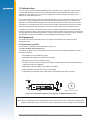
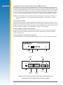
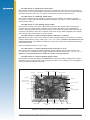
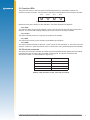
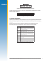
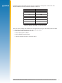
Jupiter 30
20-channel GPS receiver
module
Development kit Guide
(AA003029 series)
Related products
Jupiter 30 (standard) AA003025-G
Related documents
• Jupiter 30 Data sheet LA000576
• Jupiter 30 Product brief LA000575
• SiRF Binary Protocol reference manual
MN000314
• NMEA reference manual MN000315
• SiRFDemo and SiRFflash user guide
MN000316
LA000578A © 2006 Navman New Zealand. All rights reserved. Proprietary information and specifications subject to change without notice.
Contents
Related products................................................................................................................. 1
Related documents............................................................................................................. 1
1.0 Introduction........................................................................................................ 4
2.0 Equipment.......................................................................................................... 4
2.1 Equipment supplied....................................................................................................... 4
2.2 Equipment required....................................................................................................... 6
3.0 Technical configuration..................................................................................... 6
3.1 Overview........................................................................................................................ 6
3.1.1 Power switch (On/Off)............................................................................................ 6
3.1.2 Configuration DIP switch....................................................................................... 6
3.1.3 Function LEDs....................................................................................................... 6
3.1.4 Reset switch.......................................................................................................... 6
3.1.5 Clock out connector............................................................................................... 6
3.1.6 Serial port 1........................................................................................................... 6
3.1.7 Serial port 2........................................................................................................... 7
3.1.9 Antenna connector................................................................................................ 7
3.1.10 DC power input.................................................................................................... 7
3.2 Configuration DIP switch............................................................................................... 7
3.2.1 DIP switch 1 – GPIO3 /GYROIN input.................................................................. 7
3.2.2 DIP switch 2 – GPIO15 /FR input.......................................................................... 7
3.2.3 DIP switch 3 – BOOT from serial mode................................................................ 8
3.2.4 DIP switch 4 – GPIO1/W_TICKS input.................................................................. 8
3.2.5 DIP switch 5 – RTC backup power enable............................................................ 8
3.2.6 DIP switch 6 – Antenna preamp power select (3.3 V or 5/12 V)........................... 8
3.2.7 DIP switch 7 – Antenna preamp power select (5 V or 12 V)................................. 8
3.2.8 DIP switch 8 – Antenna preamp power enable..................................................... 8
3.3 Function LEDs............................................................................................................... 9
3.3.1 1PPS...................................................................................................................... 9
3.3.2 Power.................................................................................................................... 9
3.3.3 AUX....................................................................................................................... 9
3.3.4 GPIO..................................................................................................................... 9
3.4 Clock out connector...................................................................................................... 9
3.5 Internal configuration....................................................................................................11
3.6 Jupiter 30 module on adapter board............................................................................13
4.0 Operating instructions.................................................................................... 13
4.1 Initial connection and operation . .................................................................................13
4.2 Positioning the GPS antenna.......................................................................................14
4.3 Connecting an RTCM differential source.....................................................................14
4.4 Operating the GPS Analyser software.........................................................................15
4.4.1 VisualGPS............................................................................................................15
4.4.2 SiRFDemo............................................................................................................15
5.0 Acronyms used in this document.................................................................. 16
Figures
Figure 2-1 Equipment supplied in the Jupiter 30 GPS Development Kit............................. 4
Figure 3-1 Front and back panels of the Jupiter 30 development unit ............................... 5
Figure 3-2 Configuration DIP switch................................................................................... 7
Figure 3-5 Internal layout of the development unit.............................................................. 8
Figure 3-3 Function LEDs on front panel............................................................................ 9
Figure 3-6 Jupiter 30 adapter board..................................................................................10
Figure 3-4 Pin layout of the clock out connector................................................................11
Figure 4-1 Development unit test equipment......................................................................15
Tables
Table 3-1 DIP switch settings.............................................................................................. 7
Table 3-2 Pin functions of the clock out connector............................................................. 9
Table 3-3 Mating connector part description......................................................................11
Table 3-4 Pin functionality..................................................................................................11
Table 3-5 Signals available on the test points....................................................................12
Table 3-6 Connections J1 (2 mm pitch header) and J2 (2.54 mm pitch header)...............13
1.0 Introduction
This document provides detailed guidelines for the operation and configuration of the Jupiter
30 GPS Module Development Kit. The AA003029 series of development kits assist in the
integration of the Jupiter 30 in a customer’s application, offering a simple and easy to use
platform for evaluation purposes.
It is recommended that the user pays particular attention to the configuration settings outlined
in section 3.0 prior to applying power and operating the development unit. For example, it is
important to understand and recognise the main functional switches and connector locations
accessible on the development unit’s front and rear panels. Following this information, simple
step-by-step guidelines are presented to ensure successful setup of the development unit.
In addition to hardware, the GPS Development Kit is supplied with SiRFDemo and SiRFflash
analysis software to allow communication with the Jupiter 30 GPS receiver through a serial port.
The Windows based software presents the receiver’s raw data in a geographical form, allowing
both detailed analysis and evaluation for both NMEA and SiRF Binary formats.
2.0 Equipment
This section provides a brief overview of the equipment included in the Jupiter 30 GPS
Development Kit.
2.1 Equipment supplied
This kit should contain the items illustrated in Figure 2-1.
1. Jupiter 30 GPS development unit
The Jupiter 30 GPS receiver development unit includes all of the following hardware to allow
thorough evaluation:
• Dual RS232 level serial data I/O ports
• Selectable bias voltages for active GPS antennas
• Backup power source for SRAM and RTC
• Provision to insert a current measuring device to monitor both primary and backup power
usage under various conditions
• Regulated DC power supply to the Jupiter 30 module
• Status indication through four LEDs on front panel
• Configurable functionality using a DIP switch accessed through the front panel
(2)
(6)
(1)
Clock
Out
Serial Port 1
Serial Port 2
Antenna
DR
(3)
DC Power
9-16Volts
-
+
(4)
(5)
software and documentation
Figure 2-1 Equipment supplied in the Jupiter 30 GPS Development Kit
Note: before supplying power to the development unit, please review the configuration settings and
operation described in this document for optimum performance of the Jupiter 30 GPS receiver.
LA000578A © 2006 Navman New Zealand. All rights reserved. Proprietary information and specifications subject to change without notice.
2. GPS antenna with pre-amp, magnetic base and SMA connector
A magnetic-mount active antenna is supplied with the receiver development kit, along with an
RF cable (RG-316) already terminated with the proper connector for the development unit. The
nominal measured attenuation of the cable with connectors is approximately 5 dB. The supplied
active antenna should be biased at +3 VDC, but a different active antenna with a bias of either
+3, +5 or +12 VDC may be used. Refer to section 3.2 to ensure that the configuration switches
on the front panel of the development unit are chosen to select the appropriate bias voltage.
Caution: ensure antenna power switches are properly set before connecting the antenna. An
antenna designed for +3 VDC operation will be damaged if connected to a +12 VDC
source.
3. Serial interface cable
A serial cable is provided to interface between the development unit and the customer’s PC, or
between the development unit and a DGPS receiver. This cable is terminated at both ends with
female connectors to match the male connectors on the development unit and the PC. If the PC
used only supports a USB port, an RS232/USB converter could be utilised.
4. Power adapter for 240/120 VAC operation
DC power for the development unit is provided by either an AC/DC converter or automobile
adapter. The AC/DC converter operates from a nominal 120/240 VAC input and provides a
12 VDC at 500 mA out.
5. Power adapter for 12 VDC vehicle operation
For mobile operation, an automotive adapter intended for use in 12 VDC vehicles is provided.
'03$EVELOPMENT5NIT
1
2
CTS
0/7%2
3
4
5
206-8
6
7
8
T114
#/.&)'52!4)/.
4)-%
-!2+
0/7%2
$'03 .-%!
!#4)6% !3352%$
2%3%4
reset
function
power
configuration
‘U’ slot for
antenna
Clock
Out
Serial Port 1
SMA
antenna
Serial Port 2
Antenna
DC Power
9-16Volts
-
+
DR
1PPS
dead
reckoning
comm 1
NMEA &
comm 2
(RTCM)
DC input
Figure 3-1 Front and back panels of the Jupiter 30 development unit
(showing functional switches and connector locations)
LA000578A © 2006 Navman New Zealand. All rights reserved. Proprietary information and specifications subject to change without notice.
6. Software and documentation CD
The CD contains the Jupiter 30 GPS receiver data sheet, PC Analysis software (SiRFDemo and
SiRFflash), and other information on how to use GPS receivers.
2.2 Equipment required
The following equipment is also required to evaluate the Jupiter 30 receiver.
• IBM compatible PC
• Minimum one serial port (If your PC only has USB, a USB/RS232 converter can be
employed)
• Windows 95/98, WinNT4.0 or higher
• 486 100MHz or higher
• SVGA at least 800x600 resolution
• 16 Megabytes of RAM
• 6 Megabytes (min) of disk space
3.0 Technical configuration
This section provides a detailed description of all the technical aspects and configurable
functionality of the Jupiter 30 GPS development unit.
3.1 Overview
Figure 3-1 illustrates the connectors, switches and LEDs available on the development unit.
3.1.1 Power switch (On/Off)
The switch on the front panel controls primary power to the Jupiter 30 receiver module inside.
The power status LED (see section 3.3) indicates the state of the unit: if lit, the module has
primary power supplied. If the configuration DIP switch 5 is on and Jumper JB5/6 linked, the
module’s secondary supply SRAM and RTC will continue to be powered when the power switch
is off. Only the removal of the DC power input at the rear of the unit will stop secondary power
being applied (assuming Jumper JB5/6 and switch 5 are correctly set). Having this secondary
power supply applied means that the Jupiter 30 will have a ‘hot start’ capability when primary
power is re-applied within 4 hours, and a ‘warm start’ thereafter, by maintaining last position,
current time and satellite ephemerides.
3.1.2 Configuration DIP switch
The configuration DIP switch on the front panel provides the ability to configure the Jupiter
30 module, offering flexibility depending on the specific application. Refer to section 3.2 for a
description of the functionality of each individual switch, including the typical settings when using
the Jupiter 30 module.
3.1.3 Function LEDs
The four LEDs on the front panel provide an indication of the current status of basic features
associated with the development unit. Refer to section 3.3 for a complete description of the
function of each LED.
3.1.4 Reset switch
A reset push button is provided on the front panel to generate a receiver system hardware reset.
3.1.5 Clock out connector
The Clock out connector, located on the rear panel of the development unit, can be used to
provide module generated timing signals. Refer to section 3.4 for more detailed information.
3.1.6 Serial port 1
This host serial port is used to send and receive serial data. This port is used as the default, with
transmission in NMEA format at the rate of 9600 Baud. The connectors to be used with these
serial ports are 9-pin D-subminiature connectors.
LA000578A © 2006 Navman New Zealand. All rights reserved. Proprietary information and specifications subject to change without notice.
3.1.7 Serial port 2
This is the auxiliary serial port, and primarily used for the reception of RTCM SC-104 DGPS
(Differential GPS) correction messages.
3.1.9 Antenna connector
The antenna provided with this development kit should be connected to the SMA connector
located on the rear panel of the development unit.
3.1.10 DC power input
The supplied DC power adapter is to be plugged into the DC connector on the rear panel of
development unit. The development unit will accept voltages from 9 to 16 VDC. The middle pin
on J1 is negative polarity, while the outer shell is positive.
3.2 Configuration DIP switch
A typical setting of the Configuration DIP switch is shown in Figure 3-2.
1 2 3 4
5 6 7 8
ON
OFF
Figure 3-2 Configuration DIP switch
Table 3-1 outlines the available functionality and corresponding switch position for the
Configuration DIP switch.
Switch
Description
Typical setting
1
GPIO3/GYROIN*
OFF (high)
2
GPIO15/FR*
OFF (high)
3
Serial BOOT
OFF (normal run)
4
GPIO1/W_TICKS*
OFF (high)
5
RTC BACKUP POWER
ON (enabled)
6
PREAMP power select
OFF (3 V)
7
PREAMP power select
OFF (12 V)
8
PREAMP power enable
ON (enabled)
* These functions have been disabled by internal switch
SW3 to allow correct operation of the antenna current sense
circuits on the Jupiter 30 adapter board.
Table 3-1 DIP switch settings
A brief description of the functionality of each switch is specified below. Refer to the Jupiter 30
Data sheet for more information about the functionality of specific pads. The receiver
operating settings will not change after moving the position of a configuration switch while the
development unit is operating. Pressing the reset switch, or turning the unit off and on will enable
the settings to take effect in the receiver. The recommended method for reconfiguration is to
switch the unit off, modify the switch positions, then re-apply the power.
3.2.1 DIP switch 1 – GPIO3 /GYROIN input
DIP switch 1 interfaces with the GPIO3 /GYROIN pad of the module. The switch is typically
off, but has no effect with the standard module’s software. This switch can be enabled by the
internal switch SW3.1.
3.2.2 DIP switch 2 – GPIO15 /FR input
DIP switch 2 interfaces with the GPIO15 /FR pad of the module. The switch is typically off, but
has no effect with the standard module’s software. This switch can be enabled by the internal
switch SW3.2.
LA000578A © 2006 Navman New Zealand. All rights reserved. Proprietary information and specifications subject to change without notice.
3.2.3 DIP switch 3 – BOOT from serial mode
DIP switch 3 interfaces with the BOOT pad of the module and allows the user to upgrade the
Flash memory. For normal operation the switch should be set to off. To boot from the serial port
the switch should be set to on. This switch is enabled by the internal switch SW3.3.
3.2.4 DIP switch 4 – GPIO1/W_TICKS input
DIP switch 4 interfaces to the GPIO1/W_TICKS pad of the module. The switch is typically
off, but has no effect with the standard module’s software. This switch can be enabled by the
internal switch SW3.4.
3.2.5 DIP switch 5 – RTC backup power enable
DIP switch 5 provides control of the RTC backup power to the module. When set to the on
position, the RTC backup power is applied to the module, allowing the RTC and SRAM to
continue being powered when the primary source is removed. The jumper JB5/6 must also be
in place for the backup power to be supplied. This power supply will be supplied to the module
even with the main power switch in the off position.
3.2.6 DIP switch 6 – Antenna preamp power select (3.3 V or 5/12 V)
Dip switch 6 provides control of the antenna preamp voltage applied to the module. The switch
position determines the supply voltage (off = 3.3 V, on = 5/12 V). Switch 6 should be left in the
3.3 V (off) position. The positions of switches 7 and 8 also need to be considered when using
the preamp function.
Note: the supplied antenna is a 3.3 V type.
3.2.7 DIP switch 7 – Antenna preamp power select (5 V or 12 V)
DIP switch 7 also controls the antenna preamp voltage applied to the module. If switch 6 is
on, then switch 7 will determine the supply voltage to the active antenna (off = 12 V, on = 5 V).
Switch 7 is not operational when switch 6 is in the 3.3 V (off) position.
3.2.8 DIP switch 8 – Antenna preamp power enable
DIP switch 8 provides the ability to enable/disable the antenna preamp voltage to the module
depending on the antenna being used. Typically this switch is on, enabling 3 V to be applied to
the active antenna supplied with the kit.
serial port 2
DC power
serial port 1
DR connector
timing connector
JB10/11/12
JB13/14/15
voltage selection
switch (3.3V or 5V)
test points E1 to E9
JB1/2
JB16/17
JB3/4
SW3
all off except SW3.3
ON/OFF switch
configuration DIP
switch
function LEDS
JB5/6
reset switch
Figure 3-5 Internal layout of the development unit
LA000578A © 2006 Navman New Zealand. All rights reserved. Proprietary information and specifications subject to change without notice.
3.3 Function LEDs
There are four LEDs on the front panel of the development unit, indicating the status of a
selection of basic functions. The functions of the LEDs are described in the sections that follow.
1PPS
Power
AUX
GPIO
Figure 3-3 Function LEDs on front panel
Note that some early versions of the evaluation unit have different LED legends.
3.3.1 1PPS
This LED will flash on with each transition of the 1 PPS (Pulse Per Second) output of the GPS
receiver. The 1PPS LED will begin flashing when the receiver is tracking a satellite.
3.3.2 Power
This LED indicates presence of primary DC power to the module.
3.3.3 AUX
This LED shows activity on the auxiliary serial RS232 port (DGPS).
3.3.4 GPIO
This LED indicates the state of GPIO15 , which can be set via DIP switch 2. This LED is lit when
switch 2 is set to on. (Note that switch 2 has no effect when using standard Jupiter 30 software.)
3.4 Clock out connector
The Clock out connector provides an interface for all associated timing signals with the module.
It provides the user access to the Time Mark (1PPS) signal. The pinout connections are
described in Table 3-2, and illustrated in Figure 3-4.
Pin number
Function
1
not used
2
inverted 1PPS signal
3
normal 1PPS signal
4
ground
Table 3-2 Pin functions of the clock out connector
LA000578A © 2006 Navman New Zealand. All rights reserved. Proprietary information and specifications subject to change without notice.
J1
J2 (not normally fitted)
GPS fix LED
RTC backup battery
(not normally fitted)
power LED
Jupiter 30 module
antenna
Figure 3-6 Jupiter 30 adapter board
LA000578A © 2006 Navman New Zealand. All rights reserved. Proprietary information and specifications subject to change without notice.
10
4
3
2
1
Figure 3-4 Pin layout of the clock out connector
A mating connector for the clock out connector is supplied with the development kit. The part
number is shown in Table 3-3.
Manufacturer
Part number
Molex
70400 series ‘G’
Table 3-3 Mating connector part description
3.5 Internal configuration
It should not be necessary to open the development unit unless accessing the internal test pins.
Most combinations of I/O can be made from the front panel configuration switch. In the event
that it is necessary to open the unit, Figure 3-5 illustrates the internal layout of the development
unit board.
As shown in Figure 3-5, there is a selection of links that can be configured to provide
functionality depending on the application. Table 3-4 lists the functions available.
Pins
Function when linked
JB1/2
Current link for 5 V supply. Can be used to
determine current on 5 V rail. Not used for
the Jupiter 30 module.
JB3/4
Current link for the primary power 3.3 V
supply. Can be used to determine supply
current for 3.3 V rail.
JB5/6
Current link for the secondary power RTC
supply. Can be used to determine supply
current for RTC rail.
JB10/11
5 V supplied to Pin 1 of the DR connector
JB11/12
3.3 V supplied to Pin 1 of the DR
connector
JB13/14
not used
JB14/15
not used
JB16/17
Internal interface enable (normally fitted)
Table 3-4 Pin functionality
LA000578A © 2006 Navman New Zealand. All rights reserved. Proprietary information and specifications subject to change without notice.
11
In addition to the configurable jumpers, there is a selection of test points on the board. The
signals available on the test points are shown in Table 3-5.
Test point
Function
E1
TXA
E2
RXA
E3
TXB
E4
RXB
E6
1PPS
E7
not used
E8
ground
E9
ground
Table 3-5 Signals available on the test points
There are some settings that should not be changed when using the standard Jupiter 30 module
in conjunction with the development unit. These are as follows:
• SW2 must remain selected on 3.3 VDC
• Link for JB3/4 must be fitted
• Link for JB16/17 must be fitted
• SW3 DIP switch must be all off except SW3.3
LA000578A © 2006 Navman New Zealand. All rights reserved. Proprietary information and specifications subject to change without notice.
12
3.6 Jupiter 30 module on adapter board
Figure 3-6 (on the following page) shows the adapter board with the positions of the connectors
and indicators.
Table 3-6 lists the pin configurations for the J1 and J2 connectors.
Jupiter function
J2 (2.54 mm
pitch header)
pin no.
J1 (2 mm
pitch header)
pin no.
V_ANT
1
1
VCC_RF
2
V_BATT
3
3
VDD
4
4
M_RST
5
5
GPIO3/GYRO IN
6
6
GPIO15/FR
7
7
BOOT
8
8
GPIO1/W TICKS
9
9
RFON
10
GND
10
TXA
11
11
RXA
12
12
GPIO4
13
GND
13
TXB
14
14
RXB
15
15
Wake-up
16
GND
17
GPIO13
18
16
GND
17
GND
18
1PPS
19
GPS_FIX/GPIO10
20
19
Table 3-6 Connections J1 (2 mm pitch header) and J2 (2.54 mm pitch header)
4.0 Operating instructions
This section provides important information for the evaluation of the Jupiter 30 GPS module.
Step‑by‑step instructions for connecting and operating the GPS development kit are included for
first time setup.
4.1 Initial connection and operation
The following steps describe how to connect and operate the GPS Development Kit.
Install the supplied SiRFdemo on your PC:
1. Insert the supplied CD into the CDROM drive
2. Double click on the SiRFDemo software icon and follow the installation process.
Set up the hardware:
1. Connect the DC power adapter to the power input J1.
2. Connect the antenna cable to the SMA coaxial antenna connector on the rear panel of the
Development unit.
LA000578A © 2006 Navman New Zealand. All rights reserved. Proprietary information and specifications subject to change without notice.
13
3. Connect the DB9 serial data cable between the PC serial communication port and the
development unit’s Serial Port 1.
4. Place the antenna in a site where a good view of the sky can be seen (refer to section 4.2 for
more detail).
5. Run the GPS analyser software on the PC. (Refer to section 4.4 for more details.)
6. Connect the power supply to a suitable AC outlet.
7. Turn the unit on using the power switch on the front panel to provide primary power to the
Jupiter 30 receiver. Once power is applied, the Power LED should be lit.
4.2 Positioning the GPS antenna
The GPS antenna should be located with a clear view of the sky for optimal reception of the
satellite signals. The 1PPS LED should begin flashing at 1 Hz once the receiver is powered
and has started receiving at least one satellite. This provides an indication of whether or not the
receiver is running.
Note: GPS signals may be severely attenuated or totally obscured by roofs, solid walls, dense
foliage, or even coated glass (found in many office structures and car windows). The
development unit should be outside, or on the roof of a building to effectively evaluate
receiver performance. With stationary developments, care should be taken to keep the
antenna away from the side of a building as GPS signals can reflect off metal or coated
glass. These reflections have a longer path than direct signals and can cause multi-path
errors.
4.3 Connecting an RTCM differential source
For debugging purposes, it is suggested that users log both the GPS and RTCM data
simultaneously. To allow the provision to do this, Navman can supply a software program called
Labmon.
The development unit, PC and the RTCM SC‑104 differential correction source are connected
as shown in Figure 4.1. If RTCM SC-104 data needs to be logged at the same time it is sent
to the receiver, the OEM must supply a cable with three connectors to connect the RTCM
correction source to the development unit’s auxiliary port and to an unused serial port on the
PC. In this case, data is only logged when Labmon is invoked with file names as command line
arguments (refer to the Labmon application note LA010103). Logging and subsequent review of
the RTCM correction data often resolves performance or compatibility issues.
The development unit should be set up as shown in Figure 4-1 with only the RTCM correction
source connected to the receiver. If the RTCM cable is not connected to the receiver’s auxiliary
port, DGPS operation will not be possible. When RTCM data is being received the AUX LED will
be lit.
Note: the development unit may be connected to either the COM1, COM2, COM3, or COM4
serial ports and the RTCM differential correction data source connected either directly to
the receiver’s auxiliary I/O port, to one of the remaining serial ports of the PC, or to both
using an OEM-supplied three-connector serial cable.
LA000578A © 2006 Navman New Zealand. All rights reserved. Proprietary information and specifications subject to change without notice.
14
power
antenna
development unit
optional antenna
or pre-amplifier
RTCM DGPS
data source
monitor
PC
optional connection for logging RTCM data
Figure 4-1 Development unit test equipment
4.4 Operating the GPS Analyser software
There are two software packages supplied with the GPS Development Kit: SiRFDemo and
SiRFflash. The VisualGPS program can be obtained free of charge from the VisualGPS website
(www.visualgps.net/VisualGPS/).
4.4.1 VisualGPS
VisualGPS graphically presents the serial data transmitted by the receiver. The receiver output
must be enabled in the NMEA protocol for this software to be used.
To enable the receiver output
1. Open the VisualGPS software installed on the PC.
2. Select the Settings>Communications tab.
3. When the Communications Settings window is displayed, select the correct COM Port and set
the Baud rate to 9600 Baud.
When this has been carried out, and the development unit is powered, raw NMEA data should
appear in the NMEA Monitor Window. For more detailed information on any of the analysis
windows, use the Help function in the top toolbar.
4.4.2 SiRFDemo
SiRFDemo software can provide analysis of receiver output in either SiRF binary or NMEA
protocols. When enabled in NMEA format, the only analysis provided is raw data being
transmitted by the receiver. While the module is transmitting serial data in NMEA format, it is
LA000578A © 2006 Navman New Zealand. All rights reserved. Proprietary information and specifications subject to change without notice.
15
suggested that VisualGPS is used for analysis, rather than SiRFDemo.
To provide graphical presentation of the data, the receiver can be set to output in SiRF binary
format.
To set the receiver output to SiRF binary
1. Open the SiRFDemo software.
2. When the Data Source setup is displayed, select the appropriate COM port and 9600 Baud
from the drop down menu.
3. Select the Action menu and click on Open Data Source. If the development unit is powered,
and the serial port is connected to the PC, NMEA data should appear in the Debug View
window.
To change to SiRF binary, select the Action menu and click on the Switch to SiRF Protocol. This
should now present information in each window, similar to that of VisualGPS. Whilst enabled in
SiRF binary protocol, more of the analysis software’s functionality can be accessed. To switch
back into NMEA mode, select the Action menu and click on Switch to NMEA Protocol. Select
9600 for the baud rate and click on the Send button.
Note: settings, including the current output protocol, are reset if all power is removed from the
unit. For more information, refer to the Navman SiRFDemo and SiRFflash User Guide
MN000316.
5.0 Acronyms used in this document
1PPS: One Pulse Per Second
DGPS: Differential Global Positioning System
GPIO: General Purpose Input Output
GPS: Global Positioning System
NMEA: National Marine Electronics Association
RTC: Real Time Clock
RTCM: Radio Technical Commission for Maritime services
LA000578A © 2006 Navman New Zealand. All rights reserved. Proprietary information and specifications subject to change without notice.
16
Windows® is a trademark of Microsoft Corporation.
© 2006 Navman New Zealand. All Rights Reserved.
Information in this document is provided in connection with Navman New Zealand. (‘Navman’) products. These
materials are provided by Navman as a service to its customers and may be used for informational purposes only.
Navman assumes no responsibility for errors or omissions in these materials. Navman may make changes to
specifications and product descriptions at any time, without notice. Navman makes no commitment to update the
information and shall have no responsibility whatsoever for conflicts or incompatibilities arising from future changes to
its specifications and product descriptions. No license, express or implied, by estoppel or otherwise, to any intellectual
property rights is granted by this document. Except as provided in Navman’s Terms and Conditions of Sale for such
products, Navman assumes no liability whatsoever.
THESE MATERIALS ARE PROVIDED “AS IS” WITHOUT WARRANTY OF ANY KIND, EITHER EXPRESSED OR
IMPLIED, RELATING TO SALE AND/OR USE OF NAVMAN PRODUCTS INCLUDING LIABILITY OR WARRANTIES
RELATING TO FITNESS FOR A PARTICULAR PURPOSE, CONSEQUENTIAL OR INCIDENTAL DAMAGES,
MERCHANTABILITY, OR INFRINGEMENT OF ANY PATENT, COPYRIGHT OR OTHER INTELLECTUAL
PROPERTY RIGHT. NAVMAN FURTHER DOES NOT WARRANT THE ACCURACY OR COMPLETENESS OF THE
INFORMATION, TEXT, GRAPHICS OR OTHER ITEMS CONTAINED WITHIN THESE MATERIALS. NAVMAN SHALL
NOT BE LIABLE FOR ANY SPECIAL, INDIRECT, INCIDENTAL, OR CONSEQUENTIAL DAMAGES, INCLUDING
WITHOUT LIMITATION, LOST REVENUES OR LOST PROFITS, WHICH MAY RESULT FROM THE USE OF THESE
MATERIALS.
Navman products are not intended for use in medical, lifesaving or life sustaining applications. Navman customers
using or selling Navman products for use in such applications do so at their own risk and agree to fully indemnify
Navman for any damages resulting from such improper use or sale. Product names or services listed in this publication
are for identification purposes only, and may be trademarks of third parties. Third-party brands and names are the
property of their respective owners. Additional information, posted at www.navman.com, is incorporated by reference.
Reader Response: Navman strives to produce quality documentation and welcomes your feedback. Please send
comments and suggestions to [email protected]. For technical questions, contact your local Navman sales
office or field applications engineer.
LA000578A © 2006 Navman New Zealand. All rights reserved. Proprietary information and specifications subject to change without notice.
17