1
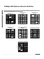
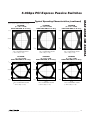
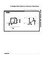
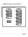
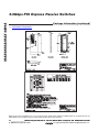
19-0770; Rev 0; 4/07
5.0Gbps PCI Express Passive Switches
The MAX4888A/MAX4889A high-speed passive switches
route PCI Express® (PCIe) data between two possible
destinations. The MAX4888A is a quad single-pole/double-throw (4 x SPDT) switch ideally suited for switching
two half lanes of PCIe data between two destinations. The
MAX4889A is an octal single-pole/double-throw (8 x
SPDT) switch ideal for switching four half lanes of PCIe
data between four destinations. The MAX4888A/
MAX4889A feature a single digital control input (SEL) to
switch signal paths.
The MAX4888A/MAX4889A are fully specified to operate from a single 3.0V to 3.6V power supply and also
operate down to +1.65V. The MAX4888A is available
in a 3.5mm x 5.5mm, 28-pin TQFN package. The
MAX4889A is available in a 3.5mm x 9.0mm, 42-pin
TQFN package. Both devices operate over the -40°C to
+85°C temperature range.
Features
o Single 1.65V to 3.6V Power-Supply Voltage
o Low Same-Pair Skew of 7ps
o Low 120µA (Max) Quiescent Current
o Supports PCIe Gen I and Gen || Data Rates
o Flow-Through Pin Configuration for Ease of
Layout
o Industry-Compatible Pinout
o Lead-Free Packaging
Ordering Information/
Selector Guide
PINPACKAGE
CONFIGURATION
PKG
CODE
MAX4888AETI+ 28 TQFN-EP*
Two
Half Lanes
T283555-1
MAX4889AETO+ 42 TQFN-EP*
Four Half
Lanes
T423590M-1
PART
Applications
Desktop Computers
Servers/Storage Area Networks
Laptops
Note: All devices are specified over the -40°C to +85°C operating temperature range.
+Denotes lead-free package.
*EP = Exposed paddle.
PCI Express is a registered trademark of PCI-Sig Corp.
Typical Application Circuit appears at end of data sheet.
Pin Configurations
NO4-
NO4+
NO3-
NO3+
NC4-
NC4+
NC3-
NC3+
V+
NO2-
NO2+
NO1-
NO1+
NC2-
8
9
10 11 12 13 14 15 16 17
GND
7
COM4-
6
COM4+
5
GND
4
V+
3
COM3-
2
COM3+
1
GND
10
SEL
9
V+
COM1+
8
18 V+
+
COM2-
N.C.
7
GND
SEL
6
N.C.
GND
5
V+
4
COM2-
3
COM2+
2
COM1-
1
V+ 42
COM2+
11 V+
+
19 GND
V+
V+ 28
MAX4889A
*EP
GND
12 GND
*EP
GND 41
COM1-
GND 27
20 V+
V+ 40
GND
13 V+
MAX4888A
21 GND
GND 39
COM1+
14 GND
V+ 26
NC2+
38 37 36 35 34 33 32 31 30 29 28 27 26 25 24 23 22
24 23 22 21 20 19 18 17 16 15
GND 25
NC1-
NC1+
NO2-
NO2+
NO1-
NO1+
V+
GND
NC2-
NC2+
NC1-
NC1+
TOP VIEW
TQFN
TQFN
*CONNECT EXPOSED PADDLE TO GROUND.
________________________________________________________________ Maxim Integrated Products
For pricing, delivery, and ordering information, please contact Maxim Direct at 1-888-629-4642,
or visit Maxim’s website at www.maxim-ic.com.
1
MAX4888A/MAX4889A
General Description
MAX4888A/MAX4889A
5.0Gbps PCI Express Passive Switches
ABSOLUTE MAXIMUM RATINGS
(All voltages referenced to GND, unless otherwise noted.)
V+ .............................................................................-0.3V to +4V
SEL, COM__, NO__, NC__ (Note 1) .............-0.3V to (V+ + 0.3V)
| COM__ - NO__ |, | COM__ - NC__ | (Note 1) ...................0 to 2V
Continuous Current (COM_ to NO__/NC__) .....................±70mA
Peak Current (COM__ to NO__/NC__)
(pulsed at 1ms, 10% duty cycle)..................................±70mA
Continuous Current (SEL).................................................±30mA
Peak Current (SEL)
(pulsed at 1ms, 10% duty cycle)................................±150mA
Continuous Power Dissipation (TA = +70°C)
28-Pin TQFN (derate 20.8mW/°C above +70°C) ....1666.7mW
42-Pin TQFN (derate 35.7mW/°C above +70°C) ....2857.1mW
Operating Temperature Range ...........................-40°C to +85°C
Storage Temperature Range .............................-65°C to +150°C
Lead Temperature (soldering, 10s) .................................+300°C
Junction Temperature ......................................................+150°C
Note 1: Signals on SEL, NO__, NC__ or COM__ exceeding V+ or GND are clamped by internal diodes. Limit forward-diode current
to maximum current rating.
Stresses beyond those listed under “Absolute Maximum Ratings” may cause permanent damage to the device. These are stress ratings only, and functional
operation of the device at these or any other conditions beyond those indicated in the operational sections of the specifications is not implied. Exposure to
absolute maximum rating conditions for extended periods may affect device reliability.
ELECTRICAL CHARACTERISTICS
(V+ = 3.0V to 3.6V, TA = -40°C to +85°C, unless otherwise noted. Typical values are at V+ = 3.3V, TA = +25°C.) (Note 2)
PARAMETER
SYMBOL
CONDITIONS
MIN
TYP
MAX
UNITS
ANALOG SWITCH
Analog-Signal Range
Voltage Between COM and
NO/NC
On-Resistance
VCOM_,
VNO_, VNC_
-0.1
(V+ - 1.2)
V
| VCOM_ VNO_ | ,
| VCOM_ VNC_ |
0
1.8
V
RON
V+ = 3.0V, ICOM_ = 15mA,
VNO_ or VNC_ = 0V, 1.8V
Ω
7
On-Resistance Match Between
Pairs of Same Channel
ΔRON
V+ = 3.0V, ICOM_ = 15mA,
VNO_ or VNC_ = 0V (Notes 3, 4)
0.1
1
Ω
On-Resistance Match
Between Channels
ΔRON
V+ = 3.0V, ICOM_ = 15mA,
VNO_ or VNC_ = 0V (Notes 3, 4)
0.6
2
Ω
0.06
2
Ω
On-Resistance Flatness
RFLAT(ON)
V+ = 3.0V, ICOM_ = 15mA
VNO_ or VNC_ = 0V, 1.8V (Notes 4, 5)
NO_ or NC_ Off-Leakage
Current
INO_(OFF)
INC_(OFF)
V+ = 3.6V, VCOM_ = 0V, 1.8V,
VNO_ or VNC_ = 1.8V, 0V
-1
+1
µA
COM_ On-Leakage
Current
ICOM_(ON)
V+ = 3.6V, VCOM_ = 0V, 1.8V,
VNO_ or VNC_ = VCOM_or unconnected
-1
+1
µA
2
_______________________________________________________________________________________
5.0Gbps PCI Express Passive Switches
(V+ = 3.0V to 3.6V, TA = -40°C to +85°C, unless otherwise noted. Typical values are at V+ = 3.3V, TA = +25°C.) (Note 2)
PARAMETER
SYMBOL
CONDITIONS
MIN
TYP
MAX
UNITS
DYNAMIC
Turn-On Time
tON
VNO_ or VNC_ = 1.0V, RL = 50Ω, Figure 1
90
250
ns
Turn-Off Time
tOFF
VNO_ or VNC_ = 1.0V, RL = 50Ω, Figure 1
10
50
ns
Propagation Delay
tPD
RS = RL = 50Ω, unbalanced, Figure 2
50
ps
Output Skew Between Pairs
tSK1
RS = RL = 50Ω, unbalanced; skew between
any two pairs, Figure 2
50
ps
Output Skew Between Same
Pair
tSK2
RS = RL = 50Ω, unbalanced; skew between
two lines on same pair, Figure 2
10
ps
On-Loss
GLOS
Crosstalk
VCT1
Signaling Data Rate
Off-Isolation
NO_/NC_ Off-Capacitance
COM_ On-Capacitance
RS = RL = 50Ω,
unbalanced,
Figure 3
Crosstalk between
any two pairs,
RS = RL = 50Ω,
unbalanced,
Figure 3
BR
RS = RL = 50Ω
VISO
Signal = 0dBm,
RS = RL = 50Ω,
Figure 3
1MHz < f < 100MHz
-0.5
500MHz < f < 1.25GHz
-1.4
f = 50MHz
-53
dB
dB
f = 1.25GHz
-32
5.0
f = 10MHz
-56
f = 1.25GHz
-26
dB
CNO_/NC_(OFF) Figure 4
CCOM_(ON)
Gbps
Figure 4
1
pF
2
pF
LOGIC INPUT
Input-Logic Low
VIL
Input-Logic High
VIH
Input-Logic Hysteresis
VHYST
Input Leakage Current
IIN
0.5
1.4
100
VSEL = 0V or V+
V
V
mV
-1
+1
µA
1.65
3.60
V
POWER SUPPLY
Power-Supply Range
V+
V+ Supply Current
I+
VSEL = 0V or V+
MAX4888A
60
MAX4889A
120
µA
Note 2: All units are 100% production tested at TA = +85°C. Limits over the operating temperature range are guaranteed by design
and characterization and are not production tested.
Note 3: ΔRON = RON (MAX) - RON (MIN).
Note 4: Guaranteed by design. Not production tested.
Note 5: Flatness is defined as the difference between the maximum and minimum value of on-resistance as measured over the
specified analog signal range.
_______________________________________________________________________________________
3
MAX4888A/MAX4889A
ELECTRICAL CHARACTERISTICS (continued)
Typical Operating Characteristics
(TA = +25°C, unless otherwise noted.)
8.0
12
7.5
7.0
TA = +25°C
10
RON (Ω)
6.5
8
TA = +85°C
12
6
10
TA = -40°C
4
TA = +25°C
8
6
4
V+ = 3.3V
2
2
5.5
5.0
0
0
-0.1 0.1 0.3 0.5 0.7 0.9 1.1 1.3 1.5 1.7 1.9 2.1
VCOM (V)
-0.1
ON-RESISTANCE vs. VCOM
(V+ = 3.3V)
10
0.2 0.3
VCOM (V)
0.4
0.5
-0.1
0.6
8
6
4
70
60
V+ = 3.3V
50
40
V+ = 2.5V
30
20
10
TA = -40°C
0
0.3
0.5 0.7
VCOM (V)
1.2
1.1
1.0
VIH
1.3
0.8
VIL
0.7
0.5
-40
tON/tOFF (ns)
1.1
0.9
-15
10
35
TEMPERATURE (°C)
60
85
1.6 1.8 2.0 2.2 2.4 2.6 2.8 3.0 3.2 3.4 3.6
SUPPLY VOLTAGE (V)
240
220
200
180
160
140
120
100
80
60
40
20
NO_ tON
MAX4888A/89A toc07
TURN-ON/-OFF TIME vs. SUPPLY VOLTAGE
NC_ tON
NO_ tOFF
NC_ tOFF
0
1.6 1.8 2.0 2.2 2.4 2.6 2.8 3.0 3.2 3.4 3.6
SUPPLY VOLTAGE (V)
4
0.9
0.6
V+ = 1.8V
0
-0.1 0.1 0.3 0.5 0.7 0.9 1.1 1.3 1.5 1.7 1.9 2.1
VCOM (V)
0.1
LOGIC THRESHOLD vs. SUPPLY VOLTAGE
MAX4888A/89A toc05
TA = +25°C
0.1
80
SUPPLY CURRENT (μA)
TA = +85°C
12
0
SUPPLY CURRENT vs. TEMPERATURE
(MAX4889A)
MAX4888A/89A toc04
14
TA = -40°C
MAX4888A/89A toc06
6.0
2
14
LOGIC THRESHOLD (V)
RON (Ω)
V+ = 2.5V
TA = +85°C
MAX4888A/89A toc03
9.0
8.5
14
RON (Ω)
V+ = 1.8V
MAX4888A/89A toc02
9.5
MAX4888A/89A toc01
10.0
ON-RESISTANCE vs. VCOM
(V+ = 2.5V)
ON-RESISTANCE vs. VCOM
(V+ = 1.8V)
ON-RESISTANCE vs. VCOM
RON (Ω)
MAX4888A/MAX4889A
5.0Gbps PCI Express Passive Switches
_______________________________________________________________________________________
5.0Gbps PCI Express Passive Switches
VCOM_+
VCOM_-
VCOM_-
EYE DIAGRAM
(V+ = 2.5V, f = 2.5GHz,
600mVP-P PRBS SIGNAL, RS = RL = 50Ω)††
MAX4888A/89A toc12
MAX4888A/89A toc11
EYE DIAGRAM
(V+ = 1.8V, f = 2.5GHz,
600mVP-P PRBS SIGNAL, RS = RL = 50Ω)††
50mV/div
VCOM_+
EYE DIAGRAM
(V+ = 3.3V, f = 2.5GHz,
600mVP-P PRBS SIGNAL, RS = RL = 50Ω)††
VCOM_+
50mV/div
50mV/div
VCOM_-
*PRBS = PSEUDORANDOM BIT SEQUENCE
† = GEN 1, 2.5Gbps; U1 = 400ps
*PRBS = PSEUDORANDOM BIT SEQUENCE
† = GEN 1, 2.5Gbps; U1 = 400ps
*PRBS = PSEUDORANDOM BIT SEQUENCE
† = GEN 1, 2.5Gbps; U1 = 400ps
VCOM_+
50ps/div
50ps/div
50ps/div
MAX4888A/89A toc12
VCOM_-
VCOM_+
50mV/div
50mV/div
50mV/div
MAX4888A/89A toc10
MAX4888A/89A toc09
MAX4888A/89A toc08
VCOM_+
EYE DIAGRAM
(V+ = 3.3V, f = 1.25GHz,
600mVP-P PRBS SIGNAL, RS = RL = 50Ω)†
EYE DIAGRAM
(V+ = 2.5V, f = 1.25GHz,
600mVP-P PRBS SIGNAL, RS = RL = 50Ω)†
EYE DIAGRAM
(V+ = 1.8V, f = 1.25GHz,
600mVP-P PRBS SIGNAL, RS = RL = 50Ω)†
VCOM_-
VCOM_25ps/div
25ps/div
*PRBS = PSEUDORANDOM BIT SEQUENCE
†† = GEN 11, 5.0Gbps; U1 = 200ps
*PRBS = PSEUDORANDOM BIT SEQUENCE
†† = GEN 11, 5.0Gbps; U1 = 200ps
25ps/div
*PRBS = PSEUDORANDOM BIT SEQUENCE
†† = GEN 11, 5.0Gbps; U1 = 200ps
_______________________________________________________________________________________
5
MAX4888A/MAX4889A
Typical Operating Characteristics (continued)
(TA = +25°C, unless otherwise noted.)
5.0Gbps PCI Express Passive Switches
MAX4888A/MAX4889A
Pin Description
PIN
6
NAME
FUNCTION
MAX4888A
MAX4889A
1, 10, 12, 14,
20, 25, 27
1, 4, 10, 14, 17,
19, 21, 39, 41
GND
2
3, 9
4
5
6
7
9
—
2
3
6
7
SEL
N.C.
COM1+
COM1COM2+
COM2-
8, 11, 13, 19,
26, 28
5, 8, 13, 18,
20, 30,
40, 42
V+
15
31
NO2-
16
32
NO2+
Analog Switch 2. Normally Open Positive Terminal.
17
33
NO1-
Analog Switch 1. Normally Open Negative Terminal.
18
34
NO1+
Analog Switch 1. Normally Open Positive Terminal.
21
35
NC2-
Analog Switch 2. Normally Closed Negative Terminal.
22
36
NC2+
Analog Switch 2. Normally Closed Positive Terminal.
23
37
NC1-
Analog Switch 1. Normally Closed Negative Terminal.
24
38
NC1+
Analog Switch 1. Normally Closed Positive Terminal.
—
11
COM3+
Analog Switch 3. Common Positive Terminal.
—
12
COM3-
Analog Switch 3. Common Negative Terminal.
—
15
COM4+
Analog Switch 4. Common Positive Terminal.
—
16
COM4-
Analog Switch 4. Common Negative Terminal.
—
22
NO4-
—
23
NO4+
Analog Switch 4. Normally Open Positive Terminal.
—
24
NO3-
Analog Switch 3. Normally Open Negative Terminal.
—
25
NO3+
Analog Switch 3. Normally Open Positive Terminal.
—
26
NC4-
Analog Switch 4. Normally Closed Negative Terminal.
—
27
NC4+
Analog Switch 4. Normally Closed Positive Terminal.
—
28
NC3-
Analog Switch 3. Normally Closed Negative Terminal.
—
29
NC3+
EP
EP
EP
Ground
Digital Control Input
No Connection. Not internally connected.
Analog Switch 1. Common Positive Terminal.
Analog Switch 1. Common Negative Terminal.
Analog Switch 2. Common Positive Terminal.
Analog Switch 2. Common Negative Terminal.
Positive-Supply Voltage Input. Connect V+ to a 1.65V to 3.6V supply voltage.
Bypass V+ to GND with a 0.1µF capacitor placed as close to the device as possible
(See the Board Layout section).
Analog Switch 2. Normally Open Negative Terminal.
Analog Switch 4. Normally Open Negative Terminal.
Analog Switch 3. Normally Closed Positive Terminal.
Exposed Paddle. Connect EP to GND.
_______________________________________________________________________________________
5.0Gbps PCI Express Passive Switches
MAX4888A/MAX4889A
3.3V
V+
COM_
NO_
OR NC_
VN_
LOGIC
INPUT
50%
VIL
VOUT
RL
t OFF
CL
SEL
VOUT
GND
LOGIC
INPUT
t r < 5ns
t f < 5ns
VIH
SWITCH
OUTPUT
0.9 x V0UT
0.9 x VOUT
0V
t ON
CL INCLUDES FIXTURE AND STRAY CAPACITANCE.
RL
VOUT = VN_
RL + RON
(
)
VN_ = VNO_ OR VNC_
Figure 1. Switching Time
_______________________________________________________________________________________
7
MAX4888A/MAX4889A
Test Circuits/Timing Diagrams
5.0Gbps PCI Express Passive Switches
MAX4888A/MAX4889A
Test Circuits/Timing Diagrams (continued)
3.3V
V+
RS
IN+
MAX4888A/MAX4889A
NO_+ OR
NC_+
COM_+
OUT+
RISE-TIME PROPAGATION DELAY = tPLHX OR tPLHY
FALL-TIME PROPAGATION DELAY = tPHLX OR tPHLY
tSK1 = DIFFERENCE IN PROPAGATION DELAY (RISE-FALL)
BETWEEN ANY TWO PAIRS
RL
RS
IN-
NO_- OR
NC_-
COM_-
tSK2 = | tPLHX - tPHLY | OR | tPHLX - tPLHY |
BETWEEN TWO LINES ON THE SAME PAIR
OUTRL
SEL
tINFALL
tINRISE
1.5V
90%
VIN+
50%
90%
50%
10%
0V
10%
1.5V
VIN-
50%
50%
0V
tOUTRISE
tPLHX
tOUTFALL
tPHLX
1.5V
90%
VOUT+
90%
50%
50%
10%
0V
10%
1.5V
50%
VOUT-
50%
0V
tPHLY
tPLHY
Figure 2. Propagation Delay and Output Skew
8
_______________________________________________________________________________________
5.0Gbps PCI Express Passive Switches
3.3V 0.1μF
V
OFF-ISOLATION = 20log OUT
VIN
NETWORK
ANALYZER
0V OR V+
V+
SEL
NC_
50Ω
VIN
COM_
V
ON-LOSS = 20log OUT
VIN
50Ω
MAX4888A/MAX4889A
CROSSTALK = 20log
VOUT
NO_
50Ω
MEAS
REF
50Ω
VOUT
VIN
50Ω
GND
MEASUREMENTS ARE STANDARDIZED AGAINST SHORTS AT IC TERMINALS.
OFF-ISOLATION IS MEASURED BETWEEN COM_ AND "OFF" NO_ OR NC_ TERMINAL ON EACH SWITCH.
ON-LOSS IS MEASURED BETWEEN COM_ AND "ON" NO_ OR NC_ TERMINAL ON EACH SWITCH.
CROSSTALK IS MEASURED BETWEEN ANY TWO PAIRS.
SIGNAL DIRECTION THROUGH SWITCH IS REVERSED; WORST VALUES ARE RECORDED.
Figure 3. On-Loss, Off-Isolation, and Crosstalk
0.1μF
two sets of eight lanes from a single 16-lane bus. The
MAX4888A/MAX4889A feature a single digital control
input (SEL) to switch signal paths.
3.3V
V+
COM_
The MAX4888A/MAX4889A are fully specified to operate from a single 3.0V to 3.6V power supply and also
operate down to 1.65V.
MAX4888A/MAX4889A
Digital Control Input (SEL)
SEL
CAPACITANCE
METER
VIL OR VIH
NC_ or
NO_
GND
The MAX4888A/MAX4889A provide a single digital
control input (SEL) to select the signal path between
the COM__ and NO__/NC__ channels. The truth tables
for the MAX4888A/MAX4889A are depicted in the
Functional Diagrams/Truth Table section. Drive SEL
rail-to-rail to minimize power consumption.
Analog Signal Levels
Figure 4. Channel Off-/On-Capacitance
Detailed Description
The MAX4888A/MAX4889A high-speed passive switches route PCIe data between two possible destinations.
The MAX4888A/MAX4889A are ideal for routing PCIe signals to change the system configuration. For example, in
a graphics application, the MAX4888A/MAX4889A create
The MAX4888A/MAX4889A accept standard PCIe signals to a maximum of V+ - 1.2V. Signals on the COM_+
channels are routed to either the NO_+ or NC_+ channels, and signals on the COM_- channels are routed to
either the NO_- or NC_- channels. The MAX4888A/
MAX4889A are bidirectional switches, allowing COM__,
NO__, and NC__ to be used as either inputs or outputs.
_______________________________________________________________________________________
9
MAX4888A/MAX4889A
Test Circuits/Timing Diagrams (continued)
5.0Gbps PCI Express Passive Switches
MAX4888A/MAX4889A
Functional Diagrams/Truth Table
V+
V+
MAX4888A
MAX4889A
COM1+
NC1+
COM1+
NC1+
COM1-
NC1-
COM1-
NC1-
NO1+
NO1+
NO1-
NO1-
COM2+
NC2+
COM2+
NC2+
COM2-
NC2-
COM2-
NC2-
SEL
NO2+
NO2+
NO2-
NO2COM3+
NC3+
COM3-
NC3NO3+
GND
NO3SEL
COM__TO COM__TO
NC__
NO__
0
ON
OFF
1
OFF
ON
COM4+
NC4+
COM4-
NC4NO4+
NO4-
SEL
GND
10
______________________________________________________________________________________
5.0Gbps PCI Express Passive Switches
DATA
DIRECTION
PCIe Switching
The MAX4888A/MAX4889A primary applications are
aimed at reallocating PCIe lanes (see Figure 5). For
example, in graphics applications, several manufacturers
have found that it is possible to improve performance
by a factor of nearly two by splitting a single 16-lane
PCIe bus into two 8-lane buses. Two of the more prominent examples are SLI™ (Scaled Link Interface) and
CrossFire™. The MAX4889A permits a computer
motherboard to operate properly with a single 16-lane
graphics card, and can later be updated to dual cards.
The same motherboard can be used with dual cards
where the user sets a jumper or a bit through software
to switch between single- or dual-card operation.
Common mode below 1V operation requirement.
ONE LANE
MAX4888A
MAX4889A
DATA IS ROUTED
TO EITHER
BOARD A OR B
NOTE: ONLY ONE LANE IS SHOWN FOR CLARITY
Board Layout
High-speed switches require proper layout and design
procedures for optimum performance. Keep designcontrolled impedance PCB traces as short as possible
or follow impedance layouts per the PCIe specification.
Ensure that power-supply bypass capacitors are
placed as close to the device as possible. Multiple
bypass capacitors are recommended. Connect all
grounds and the exposed pad to large ground planes.
Common mode below 1V operation requirement.
MAX4888A/MAX4889A
Applications Information
A
B
Figure 5. The MAX4888A/MAX4889A Used as a Single-Lane
Switch
Chip Information
PROCESS: CMOS
CrossFire is a trademark of ATI Technologies, Inc.
SLI is a trademark of NVIDIA Corporation.
______________________________________________________________________________________
11
5.0Gbps PCI Express Passive Switches
MAX4888A/MAX4889A
Typical Application Circuit
PCIe GRAPHICS INTERFACE
GRAPHICS
CARD 1
PCIe BUS
NC1+
COM1+
LANE 0 TX
LANE 1 TX
COM1-
NC1-
COM2+
NC2+
COM2-
MAX4889A
LANE 3 TX
NC2NC3+
COM3+
LANE 2 TX
GRAPHICS
CARD 2
COM3-
NC3-
COM4+
NC4+
COM4-
NC4NO1+
NO1NO2+
NO2NO3+
NO3NO4+
SEL
NO4-
CHANNEL SELECT
COM1+
LANE 0 RX
LANE 1 RX
NC1+
COM1-
NC1-
COM2+
NC2+
COM2-
MAX4889A
COM3+
LANE 2 RX
LANE 3 RX
NC2NC3+
COM3-
NC3-
COM4+
NC4+
COM4-
NC4NO1+
NO1NO2+
NO2NO3+
NO3NO4+
SEL
NO4-
CHANNEL SELECT
12
______________________________________________________________________________________
5.0Gbps PCI Express Passive Switches
28L THIN QFN.EPS
°
______________________________________________________________________________________
13
MAX4888A/MAX4889A
Package Information
(The package drawing(s) in this data sheet may not reflect the most current specifications. For the latest package outline information
go to www.maxim-ic.com/packages.)
Package Information (continued)
(The package drawing(s) in this data sheet may not reflect the most current specifications. For the latest package outline information
go to www.maxim-ic.com/packages.)
°
42L THIN QFN.EPS
MAX4888A/MAX4889A
5.0Gbps PCI Express Passive Switches
Maxim cannot assume responsibility for use of any circuitry other than circuitry entirely embodied in a Maxim product. No circuit patent licenses are
implied. Maxim reserves the right to change the circuitry and specifications without notice at any time.
14 ____________________Maxim Integrated Products, 120 San Gabriel Drive, Sunnyvale, CA 94086 408-737-7600
© 2007 Maxim Integrated Products
is a registered trademark of Maxim Integrated Products,
Products. Inc.