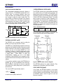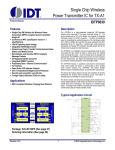
1
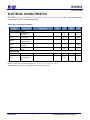
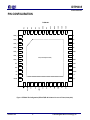
Single-Chip 5V Wireless Power Transmitter IC for TX-A5 and A11 Product Datasheet IDTP9035 Features Description 5W Solution for Wireless Power Consortium (WPC)-compliant power transmitter design A5/A11 Conforms to WPC specification version 1.1 specifications 5V±5% Operating Input Voltage Uses Full-Bridge (Integrated Half-Bridge Plus External-Half Bridge) Inverter. Closed-Loop Power Transfer Control between Base Station and Mobile Device Demodulates and Decodes WPC-Compliant Message Packets Integrated RESET Function Proprietary Back-Channel Communication I2C Interface Open-Drain LED Indicator Outputs Over-Temperature/Current Protection Security and encryption up to 64 bits Foreign Object Detection (FOD) The IDTP9035 is a highly-integrated WPC-compliant wireless power transmitter IC for power transmitter design A5 and A11. The device operates with a 5V (±5%) adaptor, and utilizes an external half-bridge in addition to its integrated half-bridge inverter to provide a highlyintegrated two-chip solution for A5/A11 transmitter applications. It controls the transferred power by modulating the switching frequency of the full-bridge inverter from 110kHz to 205kHz at a fixed 50% duty cycle specified by the WPC specification for an A5/A11 transmitter. It contains logic circuits required to demodulate and decode WPCcompliant message packets sent by the mobile device to adjust the transferred power. The IDTP9035 is an intelligent device that periodically pings the area surrounding the base station to detect a mobile device for charging while minimizing idle power. Once the mobile device is detected and authenticated, the IDTP9035 continuously monitors all communications from the mobile device, and adjusts the transmitted power accordingly by varying the switching frequency of the half-bridge inverter. The IDTP9035 features a proprietary back-channel communication mode which enables the device to communicate with IDT’s wireless power receiver solutions (e.g. IDTP9020). This feature enables additional layers of capabilities relative to standard WPC requirements. This device also features optional security and encryptions to securely authenticate the receiver before transferring power. This feature is available when an IDTP9020 is used for the receiver. Applications The device includes over-temperature/current protection and a Foreign Object Detection (FOD) method to protect the base station and mobile device from overheating in the presence of a metallic foreign object. It manages fault conditions associated with power transfer and controls status LEDs to indicate operating modes. WPC-Compliant Wireless Charging Base Stations Wireless Interface Transmitter(s) Mobile Device Receiver Control Input Power Control System Typical Application Circuit Control System Comm Cont Sensing Control Comm DeMod Comm Load Reflection Power Generation IN PWR Cont Sensing Control Mod Power Pick-Up Induction Output Load Base Station 400uF ADAPTOR 400uF 220 IDTP9035 5V_G 400nF 1 6.5uH 47 SW (4x100nF) 88uF 47 (4x22uF) GPIO_0 5V_B 10K PGND 250V 5V_A Out PWR 1.5K 1uF 2.2nF 3.3nF 47K 10K 22nF 3.3nF 15K GPIO_1 5V_E ISNS 5V_F HPF 5V_D 5V_C ` 10K 6.8nF 1nF GPIO_4 Buzzer 10K 47K 1uF GPIO_2 3 LDO2P5V LDO2P5V 1uF/25V EN EN RESET LX RESET 100K Package: 6x6-48 TQFN (See page 26) Ordering Information (See page 27) Revision 1.0.2 SCL SDA 4.7K 4.7K LEDB 1 LEDA BST SCL SDA VOSNS GPIO_3 GPIO_6 2 GND EP REFGND AGND DGND © 2012 Integrated Device Technology, Inc. IDTP9035 Product Datasheet TYPICAL APPLICATION CIRCUIT 220uF ADAPTOR IDTP9035 5V_G 220uF 220 400nF 1 6.5uH 47 SW (4x100nF) 88uF 47 (4x22uF) GPIO_0 5V_B 10K PGND 250V 5V_A 1.5K 1uF 2.2nF 3.3nF 47K 10K 22nF 3.3nF 15K GPIO_1 5V_E ISNS 5V_F HPF 5V_D 5V_C ` 10K 6.8nF 1nF GPIO_4 Buzzer 10K 47K GPIO_2 1uF 3 LDO2P5V LDO2P5V 1uF/25V EN EN RESET LX RESET 100K SCL SDA SCL SDA 4.7K 2 47K LEDA VOSNS GPIO_3 GPIO_6 4.7K LEDB BST GND EP REFGND AGND DGND Figure 1. IDTP9035 Simplified Application Schematic Note 1: NPO/C0G-type ceramic capacitor. Note 2: For PCB layout, use single-point reference (“star” ground), refer to design schematic in Figure 9). Note 3: The 220uF bulk capacitors are necessary for proper operation of the transmitter. Revision 1.0.2 2 © 2012 Integrated Device Technology, Inc. IDTP9035 Product Datasheet ABSOLUTE MAXIMUM RATINGS These absolute maximum ratings are stress ratings only. Stresses greater than those listed below (Table 1 and Table 2) may cause permanent damage to the device. Functional operation of the IDTP9035 at absolute maximum ratings is not implied. Exposure to absolute maximum rating conditions for extended periods may affect long-term reliability. Table 1. Absolute Maximum Ratings Summary. All voltages are referred to ground, unless otherwise noted. PINS MAXIMUM RATING UNITS 5V_A, 5V_B, 5V_C, 5V_D, 5V_E, 5V_F, 5V_G. THESE PINS MUST BE CONNECTED TOGETHER AT ALL TIMES. -0.3 to 6.0 V , IC_1, IC_2, SW5, GPIO_0, GPIO_1, GPIO_2, GPIO_3, GPIO_4, GPIO_5, GPIO_6, HPF, ISNS, RESET, SCL, SDA, VOSNS -0.3 to VIN+0.3 V LDO2P5V, XIN, XOUT -0.3 to 2.75 V AGND, DGND, PGND, REFGND -0.3 to +0.3 V Table 2. Package Thermal Information MAXIMUM RATING UNITS Thermal Resistance Junction to Ambient (NTG48 - TQFN) 30.8 C/W JC Thermal Resistance Junction to Case (NTG48 - TQFN) 14.6 C/W JB Thermal Resistance Junction to Board (NTG48 - TQFN) 0.75 C/W TJ Junction Temperature -40 to +150 C TA Ambient Operating Temperature -40 to +85 C TSTG Storage Temperature -55 to +150 C TLEAD Lead Temperature (soldering, 10s) +300 C SYMBOL DESCRIPTION JA Note 1:The maximum power dissipation is PD(MAX) = (TJ(MAX) - TA) / θJA where TJ(MAX) is 125°C. Exceeding the maximum allowable power dissipation will result in excessive die temperature, and the device will enter thermal shutdown. Note 2: This thermal rating was calculated on JEDEC 51 standard 4-layer board with dimensions 3” x 4.5” in still air conditions. Note 3: Actual thermal resistance is affected by PCB size, solder joint quality, layer count, copper thickness, air flow, altitude, and other unlisted variables. Note 4: For the NTG48 package, connecting the 4.1 mm X 4.1 mm EP to internal/external ground planes with a 5x5 matrix of PCB plated-through-hole (PTH) vias, from top to bottom sides of the PCB, is recommended for improving the overall thermal performance. Revision 1.0.2 3 © 2012 Integrated Device Technology, Inc. IDTP9035 Product Datasheet Table 3. ESD Information TEST MODEL PINS HBM All pins. ±2000 V CDM All pins. ±500 V Revision 1.0.2 MAXIMUM RATINGS 4 UNITS © 2012 Integrated Device Technology, Inc. IDTP9035 Product Datasheet ELECTRICAL CHARACTERISTICS = RESET = 0V, 5V_A = 5V_B = 5V_C = 5V_D = 5V_E = 5V_F = 5V_G = 5V. TA = -40 to +85C, unless otherwise noted. Typical values are at 25C, unless otherwise noted. Table 4. Device Characteristics SYMBOL DESCRIPTION CONDITIONS MIN TYP MAX UNITS 5.25 V Half-Bridge Inverter Input Supply Operating Voltage Range1 VIN IIN2 IIN_A FSW_LOW FSW_HIGH RDS(ON)_HS RDS(ON)_LS 4.75 Standby Input Current After power-up sequence complete, average including pinging. Switching Frequency at SW WPC Operating Range, in compliance with WPC requirements 20 mA 175 130 kHz kHz mΩ mΩ 110 205 Between IN and SW Between SW and PGND Inverter OCP IIN_OCP Over-Current Protection Trip Point VIN = 5V, cycle-by-cycle protection. 4 5.5 7 A 5 V V mA Low Drop Out Regulator (For Biasing Internal Circuitry Only)3 LDO2P5V3 VLDO2P5V_IN VLDO2P5V IOUT Input Voltage Range Output Voltage External Load Supplied from BUCK5VT ILoad = 2mA 5 2.5 Thermal Shutdown Thermal Shutdown TSD VIH VIL IEN ¯¯ Thermal Shutdown EN ¯¯ input current Temperature Rising Threshold Temperature Falling Threshold 140 110 C VEN ¯¯ = 5V 900 550 7.5 mV mV μA General Purpose Inputs / Outputs (GPIO) VIH VIL ILKG VOH VOL Revision 1.0.2 Input Threshold High Input Threshold Low Input Leakage Output Logic High Output Logic Low 3.5 IOH=-8mA IOL=8mA 5 -1 4 1.5 +1 0.5 © 2012 Integrated Device Technology, Inc. V V µA V V IDTP9035 Product Datasheet ELECTRICAL CHARACTERISTICS = RESET = 0V, 5V_A = 5V_B = 5V_C = 5V_D = 5V_E = 5V_F = 5V_G = 5V. TA = -40 to +85C, unless otherwise noted. Typical values are at 25C, unless otherwise noted. Table 5. Device Characteristics, Continued SYMBOL DESCRIPTION CONDITIONS MIN TYP MAX UNITS 1.5 +1 V V µA RESET VIH VIL ILKG SCL, SDA Input Threshold High Input Threshold Low Input Leakage (I2C Clock Frequency fSCL Clock Frequency fSCL Clock Frequency Hold Time (Repeated) for START Condition tHD;DAT Data Hold Time tLOW tHIGH Clock Low Period Clock High Period Set-up Time for Repeated START Condition Bus Free Time Between STOP and START Condition Capacitive Load for Each Bus Line SCL, SDA Input Capacitance Input Threshold Low Input Threshold High Leakage Current Output Logic Low (SDA) tSU;STA TBUF CB CBIN VIL VIH ILKG VOL Revision 1.0.2 -1 Interface) fSCL tHD;STA 3.5 EEPROM loading, Step 1, IDTP9035 as Master EEPROM loading, Step 2, IDTP9035 as Master IDTP9035 as Slave I2C-bus devices 100 kHz 300 kHz 0 400 0.6 μs 10 ns 1.3 0.6 μs μs 100 ns 1.3 μs 100 5 When powered by device 5V 6 pF pF 1.5 V 1.0 µA 0.5 V 3.5 -1.0 IPD= 2mA (Note 1) kHz V © 2012 Integrated Device Technology, Inc. IDTP9035 Product Datasheet ELECTRICAL CHARACTERISTICS = RESET = 0V, 5V_A = 5V_B = 5V_C = 5V_D = 5V_E = 5V_F = 5V_G = 5V. TA = -40 to +85C, unless otherwise noted. Typical values are at 25C, unless otherwise noted. Table 6. Device Characteristics, Continued SYMBOL DESCRIPTION CONDITIONS MIN Analog-to-Digital Converter ADC Conversion N Resolution fSAMPLE Sampling Rate Number of Channels Channel at ADC MUX input ADC Clock ADCCLK Frequency Full-Scale Input VIN_FS Voltage TYP MAX UNITS 12 Bit 62.5 KSPS 8 1 MHz 2.5 V 40 MHz 2.5 V Microcontroller FCLOCK VMCU Clock Frequency MCU Supply Voltage from internal 2.5V LDO Note 1 5V_A = 5V_B = 5V_C = 5V_D = 5V_E = 5V_F = 5V_G. These pins must be connected together at all times. Note 2: This current is the sum of the input currents for 5V_A = 5V_B = 5V_C = 5V_D = 5V_E = 5V_F = 5V_G. Note 3: LDO2P5V is intended only as an internal device supply and must not be loaded. Revision 1.0.2 7 © 2012 Integrated Device Technology, Inc. IDTP9035 Product Datasheet BLOCK DIAGRAM 5V_G 5V_B 5V_F LDO2P5V 5V_D 5V_C 5V_E __ EN IBIAS THSHDN Enable Sequence LDO2P5V UVLO_ 2P5V Current Limit REF Driver Control 5V_A Driver Control REF ISNS SW Demodulator GND PGND SCL SDA TEMP I2C ISNS OTP ADC Micro Controller Unit (MCU) VOSNS MCU Peripherals RAM ROM HPF VOSNS GPIO VINSNS GPIO_<6:0> 5V_A RESET Clock Generation RC OSC PLL IDTP9035 Figure 2. IDTP9035 Internal Functional Block Diagram Revision 1.0.2 8 © 2012 Integrated Device Technology, Inc. IDTP9035 Product Datasheet PIN CONFIGURATION NC NC NC NC NC GND NC HPF ISNS 5V_G 5V_G 5V_G TQFN-48L 48 47 46 45 44 43 42 41 40 39 38 37 GPIO_6 1 36 NC GPIO_5 2 35 SW GPIO_4 3 34 SW GPIO_3 4 33 SW GPIO_2 5 32 PGND GPIO_1 6 31 NC GPIO_0 7 30 PGND SCL 8 29 PGND SDA 9 28 PGND NC 10 27 VOSNS NC 11 26 IC_2 RESET 12 25 5V_F 20 5V_C 5V_D IC_1 21 22 23 24 5V_E 19 NC 18 DGND 17 AGND 16 LDO2P5V 15 5V_A 14 REFGND EN 13 5V_B EP (Center Exposed Pad) Figure 3. IDTP9035 Pin Configuration (NTG48 TQFN-48L 6.0 mm x 6.0 mm x 0.75 mm, 0.4mm pitch) Revision 1.0.2 9 © 2012 Integrated Device Technology, Inc. IDTP9035 Product Datasheet PIN DESCRIPTION Table 7. IDTP9035 NTG48 Package Pin Functions by Pin Number () PIN NAME TYPE DESCRIPTION 1 GPIO_6 I/O General purpose input/output 6 2 GPIO_5 I/O General purpose input/output 5 3 GPIO_4 I/O General purpose input/output 4 4 GPIO_3 I/O General purpose input/output 3 5 GPIO_2 I/O General purpose input/output 2 6 GPIO_1 I/O General purpose input/output 1 7 GPIO_0 I/O General purpose input/output 0 8 SCL I/O I2C clock 9 SDA I/O I2C data 10 NC NC Must be connected to GND. 11 NC NC Must be left unconnected. 12 RESET I Active-high chip reset pin. A 1µF ceramic capacitor must be connected between this pin and LDO5V, and a 100kΩ resistor to G D. I Active-low enable pin. Device is suspended and placed in low current (sleep) mode when pulled high. Tie to GND for stand-alone operation. 13 14 REFGND - Signal ground connection. Must be connected to AGND. 15 5V_A1 I A 0.1µF ceramic capacitor must be connected between this pin and GND. This pin must be connected to pins 16, 18, 19, 24, 25, 37, 38, and 39. 16 5V_B1 I A 1µF ceramic capacitor must be connected between this pin and GND. This pin must be connected to pins 15, 18, 19, 24, 25, 37, 38, and 39. 17 LDO2P5V2 O 2.5V LDO output. A 1µF ceramic capacitor must be connected between this pin and GND. 18 5V_C1 I 2.5V LDO input. A 10µF and a 0.1μF ceramic capacitor must be connected between this pin and GND. This pin must be connected to pins 15, 16, 19, 24, 25, 37, 38, and 39. 19 5V_D1 I Power and digital supply input to internal circuitry. This pin must be connected to pins 15, 16, 18, 24, 25, 37, 38, and 39. Revision 1.0.2 10 © 2012 Integrated Device Technology, Inc. IDTP9035 Product Datasheet Table 7. IDTP9035 NTG48 Package Pin Functions by Pin Number () PIN NAME TYPE DESCRIPTION 20 IC_1 NC 21 AGND - Analog ground connection. Connect to signal ground. Must be connected to REFGND. 22 DGND - Digital ground connection. Must be connected to GND. 23 NC NC 24 5V_E1 I Power supply input. Connect 0.1µF and 1µF ceramic capacitors between this pin and PGND. This pin must be connected to pins 15, 16, 18, 19, 25, 37, 38, and 39. 25 5V_F1 I This pin must be connected to pins 15, 16, 18, 19, 24, 37, 38, and 39. 26 IC_2 NC 27 VOSNS I Must be connected to GND. 28 PGND - Power ground. 29 PGND - Power ground. 30 PGND - Power ground. 31 NC NC 32 PGND - 33 SW O 34 SW O 35 SW O 36 NC NC 37 5V_G1 I 38 5V_G1 I 39 5V_G1 I 40 ISNS O Revision 1.0.2 Internal connection, do not connect. Not internally connected. Internal connection, do not connect. Not internally connected. Power ground. Pins 33, 34, and 35 must be connected together. Inverter switch node. Must be connected to capacitor in series with TX-A5 or A11 coil. Not internally connected. Inverter power supply input. Connect at least four 22µF x 25V ceramic capacitors, two 220uF x 6.3V low-ESR electrolytic chip capacitors, and a 0.1μF capacitor between this pin and ground, as close to the pin as possible. Connect all three pins, in parallel, to pins 15, 16, 18, 19, 24, 25. ISNS output signal 11 © 2012 Integrated Device Technology, Inc. IDTP9035 Product Datasheet Table 7. IDTP9035 NTG48 Package Pin Functions by Pin Number () PIN NAME TYPE DESCRIPTION 41 HPF I 42 NC NC 43 GND - 44 NC NC Internal connection, must be connected to GND. 45 NC NC Internal connection, must be connected to GPIO6. 46 NC NC Internal connection, must be connected to GPIO5. 47 NC NC Internal connection, must be connected to GPIO2. 48 NC NC Internal connection, do not connect. EP Center Exposed Pad Thermal High pass filter input Internal connection, must be connected to GND. Ground EP is on the bottom of the package and must be electrically tied to GND. For thermal performance, solder to a large copper pad embedded with a pattern of plated through-hole vias. The die is not electrically bonded to the EP, and the EP must not be used as currentcarrying electrical connection. Note 1: 5V_A, 5V_B, 5V_C,5V_D, 5V_E, 5V_F, 5V-G . These pins must be connected together at all times. Note 2: LDO2P5V is intended only as an internal device supply and must not be loaded. Revision 1.0.2 12 © 2012 Integrated Device Technology, Inc. IDTP9035 Product Datasheet TYPICAL PERFORMANCE CHARACTERISTICS , 5V_A = 5V_B = 5V_C = 5V_D = 5V_E = 5V_F = 5V_G = 5V, TA = 25oC. Unless otherwise noted. System Efficiency (ε) vs. Iout (A) 0.7 System Efficiency (ε) 0.6 0.5 0.4 0.3 0.2 0.1 0 0 0.1 0.2 0.3 0.4 0.5 0.6 0.7 0.8 0.9 1 Iout (A) Figure 4. Efficiency vs. RX Output Power with IDTP9020 Receiver Figure 5. Spacing between TX and RX coils is 2 mm Revision 1.0.2 13 © 2012 Integrated Device Technology, Inc. IDTP9035 Product Datasheet SYSTEMS APPLICATIONS DIAGRAM Inverter Cp + Ls - Modulation Cm Load Lp C Cd Rm Power 220uF ADAPTOR Modulation Cs IDTP9035 5V_G 220uF 220 400nF 1 6.5uH 47 EN EN SW 10K (4x100nF) 88uF ZREF_P 47 22nF ACM_P (4x22uF) IN_P 183nF GPIO_0 5V_B IN_P IN_P 10K PGND 11.4uH 5V_A 1uF 2.2nF 3.3nF 47K 10K 22nF REC_OUT REC_OUT REC_OUT REC_OUT 40uF 2nF 250V IN_M 1.5K IN_M IN_M 3.3nF 22nF 15K 330nF GPIO_1 IDTP9020 330nF USB/ADP_IN PGND ACM_M ZREF_M USB_IN USB_OUT 5V_E BUCK5VR_IN ISNS 5V_F HPF 5V_D 5V_C ` REC_OUT 10K 6.8nF 10K 47K 1uF GPIO_2 REC_OUT LDO2P5V EN ISNS LDO2P5V_IN LDO5V LDO5V 1uF 1uF BUCK5VR BST BUCK5VR LDO2P5V LDO2P5V 1uF SCL SDA 4.7K VOSNS LDO5V 100 GPIO_3 GPIO_6 4.7K GND EP REFGND GPIO _6 RESET RESET GPIO _5 100K 2 47K LEDA BST LX 100K LEDB BUCK5VR 10uF 47nF LDO2P5V_IN EN RESET SCL SDA REG_IN 1uF LDO2P5V 1uF/25V RESET 4.7uF 47nF GND 3 BUCK5VR_SNS LX LX LX 1nF GPIO_4 Buzzer BUCK5VR_IN BUCK5VR_IN 10uF GPIO _4 LDO5V AGND DGND 2.7K SCL SDA GPIO _3 2.7K SCL SDA REFGND AGND DGND GPIO_6 5K GPIO_5 5K GPIO_4 5K GPIO_3 5K GPIO _2 GPIO _1 GPIO _0 GPIO_2 GPIO_1 100nF 5K GPIO_0 5K Figure 6. IDTP9035/IDTP9020 Simplified Systems Application Diagram Revision 1.0.2 14 © 2012 Integrated Device Technology, Inc. IDTP9035 Product Datasheet THEORY OF OPERATION The IDTP9035 is a highly-integrated WPC1 (Wireless Power Consortium)-compliant wireless power charging IC solution for the transmitter base station. It can deliver more than 5W of power to the receiver when used with the IDTP9020 or 5W in WPC “Qi” mode using near-field magnetic induction as a means to transfer energy. It is the industry’s first 5V single-chip WPC-compliant solution designed to drive a WPC-compliant Type-A5/A11 transmitter coil. OVERVIEW Figure 2 shows the block diagram of the IDTP9035. When 5V is applied at the 5V_A-G pins with EN ¯¯ at a logic LOW, the Enable Sequence circuitry activates the voltage reference, the 2.5V LDO, and the Driver Control for the output inverter. The voltage at the output of the LDO is monitored to ensure that it remains in regulation, and the adaptor voltage, coil current, and internal temperature are monitored for proper operation. The Driver Control block converts a PWM signal (generated by the digital block and MCU) to the gate drive signals required by the output inverter to drive the external field-generating coil. Communication packets from the receiver in the mobile device are recovered by the Demodulator and converted to digital signals that can be read by the MCU. Several internal voltages are converted to their digital representations by the ADC and supplied to the MCU. Three GPIO ports are available to the system designer for driving LEDs and a buzzer. The clock for the MCU and other circuitry is generated an internal RC oscillator. I2C SDA and SCL pins permit communication with an external device or host. OVER-CURRENT/TEMPERATURE PROTECTION The current in the inverter is monitored by an analog Current Limit block. If the instantaneous coil current exceeds the OCP level, the upper switch in the inverter will be turned off and the lower switch will be turned on for the remainder of the cycle. The internal temperature is also monitored, and the part is temporarily deactivated if the temperature exceeds 140°C and reactivated when the temperature falls below 110°C. DRIVER CONTROL BLOCK and INVERTER The Driver Control block contains the logic, shoot-through protection, and gate drivers for the on-chip power FETs and external FETs. The on-chip and external FETs are configured as a full-bridge power inverter, effectively doubling the peak-to-peak voltage applied to the coil. The frequency of the full-bridge output waveform is set by the MCU. (For details, please refer to the simplified application diagram (Figure 1) and the reference design schematic (Figure 9)). DEMODULATOR Power is transferred from the transmitter to the receiver through the coupling of their respective coils: a looselycoupled transformer. The amount of power transferred is determined by the transmitter’s switching frequency (110kHz-205kHz, by WPC1), and is controlled by the receiver through instructions it sends back through the coils to the transmitter to change its frequency, end power transfer, or do something else. The instructions take the form of data packets, which are coupled through a series of filters connected to the IDTP9035’s Demodulator through the HPF pin. Recovering the data packets is the function of the Demodulator. Decoding and executing the packets is one of the functions of the MCU. MICRO-CONTROLLER UNIT (MCU) Note 1 Refer to the WPC specification http://www.wirelesspowerconsortium.com/ for the most current information Revision 1.0.2 15 at The IDTP9035’s MCU processes the algorithm, commands, and data that control the power transferred to the reciever. The MCU is provided with RAM and ROM, and parametric trim and operational modes are set at the factory through the One-Time Programming (OTP) block, read by the MCU at power-up. © 2012 Integrated Device Technology, Inc. IDTP9035 Product Datasheet APPLICATIONS INFORMATION SYSTEM FEEDBACK CONTROL (WPC) The recommended applications schematic diagram is shown in Figure 9. The IDTP9035 operates with a 5VDC (±0.25V) input. The switching frequency varies from 110kHz to 205kHz. At the 205kHz limit the duty cycle is also changed to adjust the power transfer level. The power transfer is controlled via changes in the switching frequency and duty cycle. The base or TX-side has a series resonance circuit made of a WPC Type-A5 or A11 coil (~6.3H) and a series resonant capacitor (~400nF) driven by a full-bridge inverter, as shown in Figure 7. The IDTP9035 contains logic to demodulate and decode error packets sent by the mobile device (Rx-side), and adjusts power transfer accordingly. The IDTP9035 varies the switching frequency of the full-bridge inverter between 110kHz to 205 kHz to adjust power transfer. The mobile device controls the amount of power transferred via a communication link that exists from the mobile device to the base station. The mobile device (IDTP9020-based or another WPC-compliant receiver) communicates with the IDTP9035 via communication packets. Each packet has the following format: Table 5 – Data Packet Format. IDTP9035 5V + - Preamble Fsw Header Message Checksum Driver The overall system behavior between the transmitter and receiver follows the state machine diagram below: Figure 7. Full-Bridge inverter TX Coil Driver. EXTERNAL CHIP RESET and EN ¯¯ The IDTP9035 can be externally reset by pulling the RESET pin to a logic high (above the VIH level). The RESET pin is a dedicated high-impedance active-high digital input, and the effect is similar to the power-up reset function. Because of the internal low voltage monitoring scheme, the use of the external RESET pin is not mandatory. If desired, a manual external reset scheme can be added by connecting 5V to the RESET pin through a simple switch. When RESET is HIGH, the microcontroller’s registers are set to the default configuration. When the RESET pin is released to a LOW, the microcontroller starts executing the code from the boot address. If the particular application requires the IDTP9035 to be disabled, this can be accomplished with the EN ¯¯ pin. When the EN ¯¯ pin is pulled high, the device is suspended and placed in low current (sleep) mode. If pulled low, the device is active. Figure 8. System state machine diagram The IDTP9035 performs four phases: Selection, Ping, Identification & Configuration, and Power Transfer. START (SELECTION) PHASE The current into EN ¯¯ is approximately equal to: In this phase, the IDTP9035 operates in a low power mode to determine if a potential receiver has been placed on the coil surface prior to the PING state. Twice a second, the IDTP9035 applies a brief AC signal to its coil and listens for a response. , or close to zero if V(EN ¯¯) is less than 2V. Revision 1.0.2 16 © 2012 Integrated Device Technology, Inc. IDTP9035 Product Datasheet PING PHASE Required packet(s) in ID & Config: 1. 2. 3. In this phase, the IDTP9035 applies a power signal at 175 kHz with a fixed 50% duty cycle and attempts to establish a communication link with a mobile device. Required packet(s) in PING: * If 1. Signal strength packet (0x01) The mobile device must send a Signal Strength Packet within a time period specified by the WPC, otherwise the power signal is terminated and the process repeats. Ext bit of 0x71 packet is set to 1. Also, the IDTP9035 must correctly receive the following sequence of packets without changing the operating point (175 kHz @ 50% duty cycle): 1. 2. The mobile device calculates the Signal Strength Packet value, which is an unsigned integer value between 0-255, based on this formula: where U is a monitored variable (i.e. rectified voltage/current/power) and Umax is a maximum value of that monitored variable expected during the digital ping phase at 175 kHz. If the IDTP9035 does not detect the start bit of the header byte of the Signal Strength Packet during the Ping Phase, it removes the power signal after a delay. If a signal strength packet is received, the IDTP9035 goes to the Identification and Configuration Phase. If the IDTP9035 does not move to the Identification and Configuration Phase after receiving the signal strength packet, or if a packet other than a signal strength packet is received, then power is terminated. IDENTIFICATION AND CONFIGURATION (ID & Config) In this phase, the IDTP9035 tries to identify the mobile device and collects configuration information. Identification packet (0x71) Extended Identification packet (0x81)* Configuration packet (0x51) a. b. c. d. 3. Identification Packet (0x71) Extented Identification (0x81) Up to 7 optional Configuration Packets from the following set: Power Control Hold-Off Packet (0x06) Proprietary Packet (0x18 – 0xF2) Reserved Packet Configuration Packet (0x51) If the IDTP9035 does not detect the start bit of the header byte of the next packet in the sequence within a WPCspecified time after receiving the stop bit of the checksum byte of the preceding Signal Strength Packet, then the Power Signal is removed after a delay. If a correct control packet in the above sequence is received late, or if control packets that are not in the sequence are received, the IDTP9035 removes the Power Signal after a delay. POWER TRANSFER PHASE In this phase, the IDTP9035 adapts the power transfer to the receiver based on control data it receives in control error packets. Required packet(s) in Power Transfer: 1. Control Error Packet (0x03) 2. Rectified Power Packet (0x04) For this purpose, the IDTP9035 may receive zero or more of the following Packets: 1. 2. 3. 4. 5. 6. Revision 1.0.2 17 Control Error Packet (0x03) Rectified Power Packet (0x04) Charge Status Packet (0x05) End Power Transfer Packet (0x02) Any Proprietary Packet Any Reserved Packets © 2012 Integrated Device Technology, Inc. IDTP9035 Product Datasheet If the IDTP9035 does not correctly receive the first Control Error Packet in time, it removes the Power Signal after a delay. Because Control Error Packets come at a regular interval, the IDTP9035 expects a new Control Error Packet after receiving the stop bit of the checksum byte of the preceding Control Error Packet. If that does not happen, then the IDTP9035 removes the Power Signal. Similary, the IDTP9035 must receive a Rectified Power Packet within a WPC-specified time after receiving the stop bit of the checksum byte of the Configuration Packet (which was received earlier in the identification and configuration phase). Otherwise, it removes the Power Signal. Upon receiving a Control Error value, the IDTP9035 makes adjustments to its operating point after a delay to enable the Primary Coil current to stabilize again after communication. If the IDTP9035 correctly receives a Packet that does not comply with the sequence, then it removes the Power Signal. FOREIGN OBJECT DETECTION (FOD) In addition to over-temperature protection, the IDTP9035 employs a proprietary FOD technique which detects foreign objects placed on the base station. The FOD algorithm is multi-layered and may issue warnings and/or change device operation depending on the severity of the issue. FOD is an optional feature that is not included in the standard firmware. Please contact IDT to incorporate this feature into a specific product, indicating volume and business case. Revision 1.0.2 18 © 2012 Integrated Device Technology, Inc. IDTP9035 Product Datasheet APPLICATIONS INFORMATION Figure 9. IDTP9035 WPC “Qi” Compliance Schematic (See IDTP9035 Evaluation Kit User Manual for complete details) Revision 1.0.2 19 © 2012 Integrated Device Technology, Inc. IDTP9035 Product Datasheet Table 6. IDTP9035 WPC “Qi” Compliance Bill of Materials Item 1 2 3 4 5 6 7 8 9 10 11 12 13 14 15 16 17 18 19 20 21 22 23 24 25 26 27 28 29 30 31 32 33 34 35 36 37 38 39 40 41 42 Quantity 1 4 4 1 2 1 2 1 1 4 1 1 1 1 1 2 1 1 1 1 1 1 1 1 1 1 1 2 2 1 3 1 1 1 2 1 1 3 1 1 2 1 43 Reference BZ1 C3,C29,C30,C31 C5,C8,C26,C33 C6 C9,C17 C15 C16,C39 C18 C19 C20,C21,C22,C25 C24 C27 C28 C40 D1 D2,D4 D3 D5 D6 J1 J3 L1 L2 Q2 Q4 Q6 RESET R6,R10 R7,R9 R8 R14,R32,R40 R16 R26 R27 R28,R29 R30 R31 R33,R34,R39 R38 R41 R42,R43 U1 1 U3 Part NP 1uF 0.1uF 10uF 22uF NP 220uF/6.3V 6.8nF 3.3nF 100nF/100V/C0G 1nF 22nF/50V 3.3nF/100V 2.2nF RED Schottky GREEN NP Diode I2C connector AC Adapter 6.5uH EMI Filter SiB4500BDY ZXMN3B01 SiB488DK TEST POINT 4.7K 47 220 10K 390 10K 47K NP 10K 1.5K 2.7K 100K 15K 0 IDTP9035 IC EEPROM 64KBIT 400KHZ Part_Number PS1240P02CT3 (Optional) C1608X7R1E105K GRM188R71H104KA93D C2012X5R1E106M GRM31CR61E226KE15L NP 6TPF220M9L C1005X7R1H682K C1005X7R1H332K C4532C0G2A104J C1005X7R1H102K C1608X7R1H223K C1608X7R2A332K UMK105B7222KV-F L29K-G1J2-1-0-2-R18-Z (Optional) PMEG2020EJ LG L29K-G2J1-24-Z (Optional) NP BAV21W-7-F 5103308-1 PJ-018AH WT-505060-10K2-A11-G NP SI4500BDY-T1-E3 ZXMN3B01FTA SIB488DK-T1-GE3 NP ERJ-2GEJ472X ERJ-3GEYJ470V ERJ-3GEYJ221V ERJ-3GEYJ103V ERJ-3GEYJ391V RC0402FR-0710KL ERJ-2GEJ473X NP ERJ-3EKF1002V ERJ-3EKF1501V ERJ-2GEJ272X ERJ-2GEJ104X ERJ-3GEYJ153V ERJ-8GEY0R00V IDTP9035 PCB Footprint buzz_ps1240 24AA64T-I/MNY DFN8 Note 1: Recommended capacitor temperature/dielectric and voltage ratings: 100V capacitors are recommended because >50Vp-p voltage levels may appear on the resonance capacitors as stated in the WPC specification. C0G/NPO-type capacitor values stay relatively constant with voltage while X7R and X5R ceramic capacitor values change from -40% to over -80%, with the applied voltage. The decision to use lower voltage 50V capacitors or other type temperature/dielectric capacitors is left to the end user. Revision 1.0.2 603 603 805 1206 402 POSCON_SVPF 402 402 1812 402 603 603 402 0603_DIODE SOD323 0603_DIODE sod523 SOD123 LOPRO8PIN01INREVB CONN_POWER_JACK5_5MM IND_Y31-60014F clcft_na6054 soic8 SOT23_3 sc75_6ld_fet test_pt30dpad 402 603 603 402 603 402 402 603 603 603 402 402 603 1206 NTG_48LD_6X6MM_0P4PITCH External Components The IDTP9035 requires a minimum number of external components for proper operation (see the BOM in Table 20 © 2012 Integrated Device Technology, Inc. IDTP9035 Product Datasheet 10). A complete design schematic compliant to the WPC “Qi” standard is given in Figure 9. It includes WPC “Qi” LED and buzzer signaling. GPIO4: AC or DC buzzer (optional) with resistor options for different buzzer configurations (Not Yet Available). I2C Communication GPIO6: Red LED_A to indicate standby, fault conditions, and FOD warnings. Table 7 lists how the red and green LEDs can be used to display information about the IDTP9035’s operating modes. The table also includes information about external resistors or internal pull up/down options to select LED modes. Eight of the ten LED modes (those associated with advanced charging modes) are currently designated as “Future” modes. The IDTP9035 includes an I2C block which can support either I2C Master or I2C Slave operation. After power-onreset (POR), the IDTP9035 will initially become I2C Master for the purpose of uploading firmware from an external memory device, such as an EEPROM. The I2C Master mode on the IDTP9035 does not support multi-master mode, and it is important for system designers to avoid any bus master conflict until the IDTP9035 has finished any firmware uploading and has released control of the bus as I2C Master. After any firmware uploading from external memory is complete, and when the IDTP9035 begins normal operation, the IDTP9035 is normally configured by the firmware to be exclusively in I2C Slave mode. LED FUNCTIONS Two GPIOs are used to drive LEDs which indicate, through various on/off and illumination options, the state of charging and some possible fault conditions. For maximum flexibility, the IDTP9035 tries to communicate with the first address on the EEPROM at 100kHz. If no ACK is received, communication is attempted at the other addresses at 300kHz. A red L D indicates various Fault and FOD (“Foreign Object Detection”) states. The green L D indicates Power Transfer and Charge Complete state information. Upon power up, the two LEDs together may optionally indicate the Standby State and remain in this state until another of the defined Operational States occurs EEPROM The IDTP9035 requires an external EEPROM memory chip, pre-programmed with a standard start-up program that is automatically loaded when 5V power is applied. The IDTP9035 uses I2C slave address 0x52 to access the EEPROM. The IDTP9035 slave address is 0x39. The EEPROM can be reprogrammed to suit the needs of a specific application using the IDTP9035 software tool (see the IDTP9035-Qi Demo Board User Manual for complete details). A serial 8Kbyte (8Kx8 64Kbits) external EEPROM is sufficient. As shown in Figure 12, one or two resistors configure the defined LED option combinations. The DC voltage set in this way is read one time during power-on to determine the LED configuration. To avoid interfering with the LED operation, the useful DC voltage range must be limited to not greater than 1Vdc. LDO2P5V_OUT IDTP9035 Ra If the standard firmware is not suitable for the application, custom ROM options are possible. Please contact IDT sales for more information. IDT will provide the appropriate image in the format best suited to the application. GPIO3 Resistor to set options Overview of Standard GPIO Usage There are 7 GPIO’s on the IDTP9035 transmitter IC, of which three are available for use as follows: To ADC Rb LED Mode Resistor Configuration Figure 10. IDTP9035 LED Resistor Options. GPIO3: Green LED_B to indicate standby, power transfer, and power complete; see Table 7. LED Pattern Operational Status Definitions: Blink Slow, Fast, repeat. Revision 1.0.2 21 © 2012 Integrated Device Technology, Inc. IDTP9035 Product Datasheet Table 7 – IDTP9035 LED Resistor Optioning (Not all options supported, shaded rows are for future development). LED Control Option LED Select Resistor Value Description 1 Pull Down Standby LEDs ON 2 R1 Standby LEDs ON plus 3 R2 Standby LEDs ON plus 4 R3 Standby LEDs ON plus 5 R4 Standby LEDs ON plus 6 Pull Up Standby LEDs OFF 7 R5 Standby LEDs OFF plus 8 R6 Standby LEDs OFF plus 9 R7 Standby LEDs OFF plus 10 R8 Standby LEDs OFF plus Operational Charge Status Power LED #/ Transfer Complete Color Standby LED1- Green ON BLINK SLOW ON LED2- Red ON OFF OFF LED1- Green ON BLINK SLOW ON LED2- Red ON OFF OFF LED1- Green ON BLINK SLOW ON LED2- Red ON OFF OFF LED1- Green ON BLINK SLOW ON LED2- Red ON OFF OFF LED1- Green ON BLINK SLOW ON LED2- Red ON OFF OFF LED1- Green OFF BLINK SLOW ON LED2- Red OFF OFF OFF LED1- Green OFF BLINK SLOW ON LED2- Red OFF OFF OFF LED1- Green OFF BLINK SLOW ON LED2- Red OFF OFF OFF LED1- Green OFF BLINK SLOW ON LED2- Red OFF OFF OFF LED1- Green OFF BLINK SLOW ON LED2- Red OFF OFF OFF Fault Condition OFF ON OFF ON OFF ON OFF ON OFF ON OFF ON OFF ON OFF ON OFF ON OFF ON FOD Warning OFF BLINK FAST OFF BLINK FAST OFF BLINK FAST OFF BLINK FAST OFF BLINK FAST OFF BLINK FAST OFF BLINK FAST OFF BLINK FAST OFF BLINK FAST OFF BLINK FAST R1-R8 are created using combination of two 1% resistors. Designates Future Option power transfer is terminated, the buzzer is sounded in a repeating sequence: Buzzer Function An optional buzzer feature is supported on GPIO4. The default configuration is an “AC” buzzer. The signal is created by toggling GPIO4 active-high/active-low at a 2kHz frequency. For 30 seconds: 400ms ON, 800ms OFF, repeat Next 30 seconds: Off/silence (but no change to LED on/off patterns) The pattern is repeated while the error condition exists Buzzer Action: Power Transfer Indication The IDTP9035 supports audible notification when the device operation successfully reaches the Power Transfer state. The duration of the power transfer indication sound is 400ms. The buzzer is synchronized with the FOD LED such that the 400ms on tone corresponds with the red LED illumination and 800ms off (no sound) corresponds with the red LED being off. The latency between reaching the Power Transfer state and sounding the buzzer does not exceed 500ms. Additionally, the buzzer sound is concurrent within ±250ms of any change to the LED configuration indicating the start of power transfer. As with any high-performance mixed-signal IC, the IDTP9035 must be isolated from the system power supply noise to perform optimally. A decoupling capacitor of 0.1μF must be connected between each power supply and the PCB ground plane as close to these pins as possible. For optimum device performance, the decoupling capacitor must be mounted on the component side of the PCB. Avoid the use of vias in the decoupling circuit. Additionally, medium value capacitors in the 22μF range must be used at the 5V_G input to minimize ripple voltage Decoupling/Bulk Capacitors Buzzer Action: No Power Transfer due to Foreign Object Detected (FOD) When a major FOD situation is detected such that, for safety reasons, power transfer is not initiated, or that Revision 1.0.2 22 © 2012 Integrated Device Technology, Inc. IDTP9035 Product Datasheet and voltage droop due to the large current requirements of the Full-Bridge driver. At least four 22μF capacitors must be used close to the IN pins of the device. Since the operating voltage is 4.75V to 5.25V, the value of the capacitors will decrease due to capacitance-to-applied voltage characteristics of the commonly-used ceramic dielectrics. For example, a 22μF X7R 6.3V capacitor’s value is actually 6μF when operating at 5V. get the lowest ESR. The part numbers are shown in Table 6. LDO Input Capacitor The input capacitors must be located as physically close as possible to the power pin (5V_C) and power ground (GND). Ceramic capacitors are recommended for their higher current operation and small profile. Also, ceramic capacitors are inherently more capable than are tantalum capacitors to withstand input current surges from low impedance sources such as batteries used in portable devices. Typically, 10V- or 16V-rated capacitors are required. The recommended external components are shown in Table 10. There must also be two 220μF 6.3V OS-CON or POSCAP bulk capacitors, one connected at the node where the input voltage to the board is applied, and another at the power input to the external Half-Bridge. OS-CON and POSCAP capacitors have much lower ESR than aluminum electrolytic capacitors and will reduce voltage ripple. ADC Considerations Output Capacitor For proper load voltage regulation and operational stability, a capacitor is required on the output of the LDO. The output capacitor must be placed as close to the device and power (PGND) pins as possible. Since the LDO has been designed to function with very low ESR capacitors, a ceramic capacitor is recommended for best performance. The GPIO pins are connected internally to a successive approximation ADC with a multiplexed input. The GPIO pins that are connected to the ADC have limited input range, so attention must be paid to the maximum VIN (2.5V). 0.01μF decoupling capacitors can be added to the GPIO inputs to minimize noise. WPC TX-A5 or A11 Coil PCB Layout Considerations The SW pin connects to a series-resonance circuit comprising a WPC Type-A5 or A11 coil (~6.5H) and a series resonant capacitor (~400nF), as shown in Figure 9. The inductor serves as the primary coil in a looselycoupled transformer, the secondary of which is the inductor connected to the power receiver (IDTP9020 or another). The TX-A5 or A11 power transmitter coil is mounted on a ferrite shield to reduce EMI. The coil assembly can be mounted next to the IDTP9035. Either ground plane or grounded copper shielding can be added beneath the ferrite shield for added reduction in radiated electrical field emissions. The coil ground plane/shield must be connected to the IDTP9035 ground plane by a single trace. Resonance Capacitors Because of the need to keep the resonant frequency of the output circuit stable, the resonance capacitors must be C0G type dielectric and have a DC rating to 100V. The highest-efficiency combination is four 100nF in parallel to Revision 1.0.2 23 - For optimum device performance and lowest output phase noise, the following guidelines must be observed. Please contact IDT for Gerber files that contain the recommended board layout. - As for all switching power supplies, especially those providing high current and using high switching frequencies, layout is an important design step. If layout is not carefully done, the regulator could show instability as well as EMI problems. Therefore, use wide and short traces for high current paths. - The 0.1μF decoupling capacitors must be mounted on the component side of the board as close to the VDD pin as possible. Do not use vias between decoupling capacitors and VDD pins. Keep PCB traces to each VDD pin and to ground vias as short as possible. - To optimize board layout, place all components on the same side of the board and limit the use of vias. Route other signal traces away from the IDTP9035. For example, use keepouts for signal traces routing on inner and bottom layers underneath the device. © 2012 Integrated Device Technology, Inc. IDTP9035 Product Datasheet - The NQG48 6.0 mm x 6x0 mm x 75mm 48L package has an inner thermal pad which requires blind assembly. It is recommended that a more active flux solder paste be used such as Alpha OM-350 solder paste from Cookson Electronics (http://www.cooksonsemi.com). Please contact IDT for Gerber files that contain recommended solder stencil design. - The package center exposed pad (EP) must be reliably soldered directly to the PCB. The center land pad on the PCB (set 1:1 with EP) must also be tied to the board ground plane, primarily to maximize thermal performance in the application. The ground connection is best achieved using a matrix of PTH vias embedded in the PCB center land pad for the NTG48. The PTH vias perform as thermal conduits to the ground plane (thermally, a heat spreader) as well as to the solder side of the board. There, these thermal vias embed in a copper fill having the same dimensions as the center land pad on the component side. Recommendations for the via finished hole-size and array pitch are 0.3mm to 0.33mm and 1.3mm, respectively. - Layout and PCB design have a significant influence on the power dissipation capabilities of power management ICs. This is due to the fact that the surface mount packages used with these devices rely heavily on thermally conductive traces or pads to transfer heat away from the package. Appropriate PC layout techniques must then be used to remove the heat due to device power dissipation. The following general guidelines will be helpful in designing a board layout for lowest thermal resistance: 1. PC board traces with large cross sectional areas remove more heat. For optimum results, use large area PCB patterns with wide and heavy (2 oz.) copper traces, placed on the top layer of the PCB. 2. In cases where maximum heat dissipation is required, use double-sided copper planes connected with multiple vias. 3. Thermal vias are needed to provide a thermal path to the inner and/or bottom layers of the PCB to remove the heat generated by device power dissipation. 4. Where possible, increase the thermally conducting surface area(s) openly exposed to moving air, so that heat can be removed Revision 1.0.2 by convection (or forced air flow, if available). 5. Do not use solder mask or place silkscreen on the heat-dissipating traces/pads, as they increase the net thermal resistance of the mounted IC package. Power Dissipation/Thermal Requirements The IDTP9035 is offered in a TQFN-48L package. The maximum power dissipation capability is 2W, limited by the die’s specified maximum operating junction temperature, TJ, of 125°C. The junction temperature rises with the device power dissipation based on the package thermal resistance. The package offers a typical thermal resistance, junction to ambient (JA), of 31°C/W when the PCB layout and surrounding devices are optimized as described in the PCB Layout Considerations section. The techniques as noted in the PCB Layout section need to be followed when designing the printed circuit board layout, as well as the placement of the IDTP9035 IC package in proximity to other heat generating devices in a given application design. The ambient temperature around the power IC will also have an effect on the thermal limits of an application. The main factors influencing θJA (in the order of decreasing influence) are PCB characteristics, die/package attach thermal pad size, and internal package construction. Board designers should keep in mind that the package thermal metric θJA is impacted by the characteristics of the PCB itself upon which the TQFN is mounted. For example, in a still air environment, as is often the case, a significant amount of the heat that is generated (60 - 85%) sinks into the PCB. Changing the design or configuration of the PCB changes impacts the overall thermal resistivity and, thus, the board’s heat sinking efficiency. Implementation of integrated circuits in low-profile and fine-pitch surface-mount packages typically requires special attention to power dissipation. Many systemdependant issues such as thermal coupling, airflow, added heat sinks, and convection surfaces, and the presence of other heat-generating components, affect the power-dissipation limits of a given component. Three basic approaches for enhancing thermal performance are listed below: 1. Improving the power dissipation capability of the PCB design 2. Improving the thermal coupling of the component to the PCB 3. Introducing airflow into the system 24 © 2012 Integrated Device Technology, Inc. IDTP9035 Product Datasheet First, the maximum power dissipation for a given situation must be calculated: Thermal Overload Protection The IDTP9035 integrates thermal overload shutdown circuitry to prevent damage resulting from excessive thermal stress that may be encountered under fault conditions. This circuitry will shut down or reset the device if the die temperature exceeds 140°C. To allow the maximum load current on each regulator and resonant transmitter, and to prevent thermal overload, it is important to ensure that the heat generated by the IDTP9035 is dissipated into the PCB. The package exposed paddle must be soldered to the PCB, with multiple vias evenly distributed under the exposed paddle and exiting the bottom side of the PCB. This improves heat flow away from the package and minimizes package thermal gradients. PD(MAX) = (TJ(MAX) - TA)/θJA Where: PD(MAX) = Maximum Power Dissipation (W) θJA = Package Thermal Resistance (°C/W) TJ(MAX) = Maximum Device Junction Temperature (°C) TA = Ambient Temperature (°C) The maximum recommended junction temperature (TJ(MAX)) for the IDTP9035 device is 150°C. The thermal resistance of the 48-pin NQG package (NGQ48) is optimally θJA=30°C/W. Operation is specified to a maximum steadystate ambient temperature (TA) of 85°C. Therefore, the maximum recommended power dissipation is: PD(Max) = (150°C - 85°C) / 30°C/W Revision 1.0.2 Special Notes NQG TQFN-48 Package Assembly Note 1: Unopened Dry Packaged Parts have a one year shelf life. Note 2: The HIC indicator card for newly opened Dry Packaged Parts should be checked. If there is any moisture content, the parts must be baked for minimum of 8 hours at 125˚C within 24 hours of the assembly reflow process. 2 Watt 25 © 2012 Integrated Device Technology, Inc. IDTP9035 Product Datasheet PACKAGE OUTLINE DRAWING REVISIONS DCN REV DESCRIPTION DATE 00 INITIAL RELEASE 3/16/10 APPROVED POD IN BOTTOM VIEW 37 DAP SIZE 4.5x4.5 48 36 1 C0.35 25 12 24 13 IDT TOLERANCES UNLESS SPECIFIED POD IN SIDE VIEW DECIMAL X± .1 XX± .05 XXX± .030 APPROVALS DRAWN PKP CHECKED TM ANGULAR ±1° DATE 12/04/09 6024 SILVER CREEK VALLEY ROAD. SAN JOSE, CA 95138 PHONE: (408) 284-8200 FAX: (408) 284-3572 www.IDT.com TITLE NT/NTG48 PACKAGE OUTLINE 6.0 x 6.0 mm BODY 0.4 mm PITCH TQFN SIZE C DRAWING No. REV PSC-4294 DO NOT SCALE DRAWING 00 SHEET 1OF 1 Figure 11. IDTP9035 Package Outline Drawing (NTG48 TQFN-48L 6.0 mm x 6.0 mm x 0.75 mm48L, 0.4mm pitch) Revision 1.0.2 26 © 2012 Integrated Device Technology, Inc. IDTP9035 Product Datasheet ORDERING GUIDE Table 8. Ordering Summary PART NUMBER MARKING PACKAGE AMBIENT TEMP. RANGE SHIPPING CARRIER QUANTITY P9035-0NTGI P9035-0NTGI8 P9035NTG P9035NTG NTG48 - TQFN-48 6x6x0.75mm NTG48 - TQFN-48 6x6x0.75mm -40°C to +85°C -40°C to +85°C Tape or Canister Tape and Reel 25 2,500 www.IDT.com 6024 Silver Creek Valley Road San Jose, California 95138 Tel: 800-345-7015 DISCLAIMER Integrated Device Technology, Inc. (IDT) and its subsidiaries reserve the right to modify the products and/or specifications described herein at any time and at IDT’s sole discretion. All information in this document, including descriptions of product features and performance, is subject to change without notice. Performance specifications and the operating parameters of the described products are determined in the independent state and are not guaranteed to perform the same way when installed in customer products. The information contained herein is provided without representation or warranty of any kind, whether express or implied, including, but not limited to, the suitability of IDT’s products for any particular purpose, an implied warranty of merchantability, or non-infringement of the intellectual property rights of others. This document is presented only as a guide and does not convey any license under intellectual property rights of IDT or any third parties. IDT’s products are not intended for use in life support systems or similar devices where the failure or malfunction of an IDT product can be reasonably expected to significantly affect the health or safety of users. Anyone using an IDT product in such a manner does so at their own risk, absent an express, written agreement by IDT. Integrated Device Technology, IDT and the IDT logo are registered trademarks of IDT. Other trademarks and service marks used herein, including protected names, logos and designs, are the property of IDT or their respective third party owners. © Copyright 2012. All rights reserved.