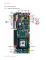
1
User’s Manual ECB-870 Intel Pentium 4 Full-size CPU Card with Dual 10/100 Base-Tx Ethernet 1st Ed. – 20 May 2002 Part No.2047870000 ECB-870 FCC STATEMENT THIS DEVICE COMPLIES WITH PART 15 FCC RULES. OPERATION IS SUBJECT TO THE FOLLOWING TWO CONDITIONS: (1) THIS DEVICE MAY NOT CAUSE HARMFUL INTERFERENCE. (2) THIS DEVICE MUST ACCEPT ANY INTERFERENCE RECEIVED INCLUDING OPERATION. INTERFERENCE THAT MAY CAUSE UNDESIRED THIS EQUIPMENT HAS BEEN TESTED AND FOUND TO COMPLY WITH THE LIMITS FOR A CLASS "A" DIGITAL DEVICE, PURSUANT TO PART 15 OF THE FCC RULES. THESE LIMITS ARE DESIGNED TO PROVIDE REASONABLE PROTECTION AGAINTST HARMFUL INTERFERENCE WHEN THE EQUIPMENT IS OPERATED IN A COMMERCIAL ENVIRONMENT. THIS EQUIPMENT GENERATES, USES, AND CAN RADIATE RADIO FREQUENCY ENERGY AND, IF NOT INSTATLLED AND USED IN ACCORDANCE WITH THE INSTRUCTION MANUAL, MAY CAUSE HARMFUL INTERFERENCE TO RADIO COMMUNICATIONS. OPERATION OF THIS EQUIPMENT IN A RESIDENTIAL AREA IS LIKELY TO CAUSE HARMFUL INTERFERENCE IN WHICH CASE THE USER WILL BE REQUIRED TO CORRECT THE INTERFERENCE AT HIS OWN EXPENSE. Evalue Technology Inc. User’s Manual Copyright Notice Copyright 2001, 2002, Evalue Technology Inc., ALL RIGHTS RESERVED. No part of this document may be reproduced, copied, translated, or transmitted in any form or by any means, electronic or mechanical, for any purpose, without the prior written permission of the original manufacturer. Trademark Acknowledgement Brand and product names are trademarks or registered trademarks of their respective owners. Disclaimer Evalue Technology Inc. reserves the right to make changes, without notice, to any product, including circuits and/or software described or contained in this manual in order to improve design and/or performance. Evalue Technology assumes no responsibility or liability for the use of the described product(s), conveys no license or title under any patent, copyright, or mask work rights to these products, and makes no representations or warranties that these products are free from patent, copyright, or mask work right infringement, unless otherwise specified. Applications that are described in this manual are for illustration purposes only. Evalue Technology Inc. makes no representation or warranty that such application will be suitable for the specified use without further testing or modification. Life Support Policy Evalue Technology’s PRODUCTS ARE NOT FOR USE AS CRITICAL COMPONENTS IN LIFE SUPPORT DEVICES OR SYSTEMS WITHOUT THE PRIOR WRITTEN APPROVAL OF Evalue Technology Inc. As used herein: 1. Life support devices or systems are devices or systems which, (a) are intended for surgical implant into body, or (b) support or sustain life and whose failure to perform, when properly used in accordance with instructions for use provided in the labelling, can be reasonably expected to result in significant injury to the user. 2. A critical component is any component of a life support device or system whose failure to perform can be reasonably expected to cause the failure of the life support device or system, or to affect its safety or effectiveness. Evalue Technology Inc. ECB-870 A Message to the Customer Evalue Customer Services Each and every Evalue’s product is built to the most exacting specifications to ensure reliable performance in the harsh and demanding conditions typical of industrial environments. Whether your new Evalue device is destined for the laboratory or the factory floor, you can be assured that your product will provide the reliability and ease of operation for which the name Evalue has come to be known. Your satisfaction is our primary concern. Here is a guide to Evalue’s customer services. To ensure you get the full benefit of our services, please follow the instructions below carefully. Technical Support We want you to get the maximum performance from your products. So if you run into technical difficulties, we are here to help. For the most frequently asked questions, you can easily find answers in your product documentation. These answers are normally a lot more detailed than the ones we can give over the phone. So please consult the user’s manual first. To receive the latest version of the user’s manual, please visit our Web site at: http://www.evalue-tech.com/ If you still cannot find the answer, gather all the information or questions that apply to your problem, and with the product close at hand, call your dealer. Our dealers are well trained and ready to give you the support you need to get the most from your Evalue’s products. In fact, most problems reported are minor and are able to be easily solved over the phone. In addition, free technical support is available from Evalue’s engineers every business day. We are always ready to give advice on application requirements or specific information on the installation and operation of any of our products. Please do not hesitate to call or email us. Headquarters Evalue Technology Inc. 5F~7, No.130, Chien Kang Road, Chung Ho City, Taipei, Taiwan Tel : +886-2-2228-6111 Fax : +886-2-2228-6667 http://www.evalue-tech.com E-mail: [email protected] Evalue Technology Inc. Europe Branch Office Evalue Europe A/S Nordre Strandvej 119C, 3150 Hellebaek, Denmark Tel : +45-7025-0310 Fax : +45-4975-5026 http://www.evalue-tech.com E-mail: [email protected] User’s Manual Product Warranty Evalue warrants to you, the original purchaser, that each of its products will be free from defects in materials and workmanship for two years from the date of purchase. This warranty does not apply to any products which have been repaired or altered by persons other than repair personnel authorized by Evalue, or which have been subject to misuse, abuse, accident or improper installation. Evalue assumes no liability under the terms of this warranty as a consequence of such events. Because of Evalue’s high qualitycontrol standards and rigorous testing, most of our customers never need to use our repair service. If any of Evalue’s products is defective, it will be repaired or replaced at no charge during the warranty period. For out-of-warranty repairs, you will be billed according to the cost of replacement materials, service time, and freight. Please consult your dealer for more details. If you think you have a defective product, follow these steps: 1. Collect all the information about the problem encountered. (For example, CPU type and speed, Evalue’s products model name, hardware & BIOS revision number, other hardware and software used, etc.) Note anything abnormal and list any on-screen messages you get when the problem occurs. 2. Call your dealer and describe the problem. Please have your manual, product, and any helpful information available. 3. If your product is diagnosed as defective, obtain an RMA (return material authorization) number from your dealer. This allows us to process your good return more quickly. 4. Carefully pack the defective product, a complete Repair and Replacement Order Card and a photocopy proof of purchase date (such as your sales receipt) in a shippable container. A product returned without proof of the purchase date is not eligible for warranty service. 5. Write the RMA number visibly on the outside of the package and ship it prepaid to your dealer. Evalue Technology Inc. ECB-870 Packing List Before you begin installing your single board, please make sure that the following materials have been shipped: 1 ECB-870 Pentium 4 Full-size single board 1 Quick Installation Guide 1 CD-ROM contains the followings: — User’s Manual (this manual in PDF file) — Ethernet driver and utilities — VGA drivers and utilities — Latest BIOS (as of the CD-ROM was made) Cable set includes the followings: — 1 ATA-33 IDE cable (40-pin, pitch 2.54mm) — 1 ATA-100 IDE cable (40-pin, pitch 2.54mm) — 1 FDD cable (34-pin, pitch 2.54mm) — 1 bracket with one Printer port cable (26-pin, pitch 2.54mm) — 1 bracket with two Serial port cable (10-pin, pitch 2.54mm) — 1 bracket with two USB port cable (10-pin, pitch 2.54mm) — 1 PS/2 keyboard and mouse Y cable (6-pin, Mini-DIN) If any of these items are missing or damaged, please contact your distributor or sales representative immediately. Evalue Technology Inc. User’s Manual 1. MANUAL OBJECTIVES .............................................................................................1 2. INTRODUCTION.........................................................................................................2 2.1 System Overview ...................................................................................................2 2.2 System Specifications ...........................................................................................3 2.3 Architecture Overview ...........................................................................................5 2.3.1 2.3.2 2.3.3 2.3.4 2.3.5 2.3.6 2.3.7 2.3.8 2.3.9 3. 82845 MCH and 82801BA ........................................................................................... 6 System Memory Interface ............................................................................................ 7 AGP Interface .............................................................................................................. 8 SiS 315 4X AGP VGA controller .................................................................................. 8 PCI Interface................................................................................................................ 8 IDE Interface (Bus Master Capability and Synchronous DMA Mode) ........................... 9 USB ............................................................................................................................. 9 Ethernet .......................................................................................................................9 M-Systems DiskOnChip ............................................................................................. 10 HARDWARE CONFIGURATION ..............................................................................11 3.1 Installation Procedure .........................................................................................11 3.2 Safety Precautions ...............................................................................................11 3.2.1 3.2.2 3.3 Warning! .................................................................................................................... 11 Caution! ..................................................................................................................... 11 Socket 478 Processor..........................................................................................12 3.3.1 3.3.2 Installing Pentium 4 CPU ........................................................................................... 12 Removing CPU .......................................................................................................... 12 3.4 Main Memory ........................................................................................................12 3.5 M-Systems’ DiskOnChip Flash Disk...................................................................13 3.5.1 3.6 Installing DOC............................................................................................................ 13 Installing the Single Board Computer ................................................................13 3.6.1 3.6.2 3.6.3 3.6.4 SiS 315 4X AGP VGA Controller ............................................................................... 14 Promise FastTrak100 UltraATA/100 IDE RAID Interface (ECB-870R Only)............... 15 Intel 82559(or 82559ER) & 82801BA(ICH2) + 82562ET (PHY) Network Controller ... 16 Drivers Support .......................................................................................................... 16 3.7 Watchdog Timer Programming...........................................................................17 3.8 Jumper & Connector............................................................................................18 3.8.1 3.8.2 Jumper & Connector Layout ...................................................................................... 18 Jumper & Connector List ........................................................................................... 19 Evalue Technology Inc. ECB-870 3.9 Setting Jumpers ...................................................................................................21 3.9.1 3.9.2 3.9.3 3.9.4 3.9.5 3.9.6 3.9.7 COM2 RS-232/422/485 Select (J1, J2, JCSEL) ......................................................... 22 LAN2 Enable / Disable Select (J82559) ..................................................................... 23 M-Systems DiskOnChip Memory Address Select (JDOC) ......................................... 23 DiskOnModule Power Select (JDOM) ........................................................................ 23 RAID Enable / Disable Select (JRAID, ECB-870R Only)............................................ 24 Clear CMOS (JRTC) .................................................................................................. 24 Watchdog Timer Select (JWDT) ................................................................................ 24 3.10 Connector Definitions..........................................................................................25 3.10.1 ATX Power Connector (ATX) ..................................................................................... 25 3.10.2 Pentium IV +12V Connector (JATXR1) ...................................................................... 25 3.10.3 CPU Fan and System Fan Connector (CPUFAN, CHASFAN) ................................... 25 3.10.4 Floppy Connector (FLOPPY) ..................................................................................... 26 3.10.5 Signal Description – Floppy Connector (FLOPPY)..................................................... 27 3.10.6 Primary IDE Connector (IDE1)................................................................................... 28 3.10.7 Secondary IDE Connector and RAID IDE Connector (IDE 2, & IDE 3, 4) .................. 29 3.10.8 Signal Description – Primary & Secondary and RAID IDE Connector (IDE 1, 2, 3, 4) 30 3.10.9 Internal Keyboard Connector (JATKB)....................................................................... 34 3.10.10 Signal Description – Internal Keyboard Connector (JATKB) ...................................... 34 3.10.11 Front Panel Connector (JFRNT) ................................................................................ 34 3.10.12 Fast & Standard IrDA Connector (JIR)....................................................................... 35 3.10.13 Signal Configuration – Fast & Standard IrDA Connector (JIR) ................................... 35 3.10.14 Serial Port 1 / 2 Connector in RS-232 (JCOM1, JCOM2)........................................... 35 3.10.15 Signal Description – Serial Port 1 / 2 in RS-232 Mode (JCOM1, JCOM2) .................. 35 3.10.16 Serial Port 1 / 2 Connector in RS-422 (JCOM1, JCOM2)........................................... 36 3.10.17 Signal Description – Serial Port 1 / 2 in RS-422 Mode (JCOM1, JCOM2) .................. 36 3.10.18 Serial Port 1 / 2 Connector in RS-485 (JCOM1, JCOM2)........................................... 37 3.10.19 Signal Description – Serial Port 1 / 2 in RS-485 Mode (JCOM1, JCOM2) .................. 37 3.10.20 ATX Power Controller (JPS) ...................................................................................... 38 3.10.21 Wake-On-LAN Connector (JWOL)............................................................................. 38 3.10.22 10/100 BASE-Tx Ethernet Connector (LAN1, LAN2) ................................................. 38 3.10.23 Signal Description – 10/100Base-Tx Ethernet Connector (LAN1, LAN2) ................... 38 3.10.24 Parallel Port Connector (PRINTER) ........................................................................... 39 3.10.25 Signal Description – Parallel Port Connector (PRINTER)........................................... 40 3.10.26 PS/2 Keyboard Connector (PS2) ............................................................................... 41 3.10.27 PS/2 Mouse Connector (PS2) .................................................................................... 41 3.10.28 Signal Description – PS/2 Mouse Connector (PS2) ................................................... 41 3.10.29 USB Connector (USBA) ............................................................................................. 42 3.10.30 Signal Description – USB Connector (USBA) ............................................................ 42 3.10.31 CRT Connector (VGA) ............................................................................................... 43 3.10.32 Signal Description – CRT Connector (VGA)............................................................... 43 4. AWARD BIOS SETUP..............................................................................................44 4.1 Starting Setup.......................................................................................................44 4.2 Using Setup ..........................................................................................................45 4.2.1 4.2.2 4.3 Navigating through the menu bar............................................................................... 45 To display a sub menu............................................................................................... 45 Getting Help..........................................................................................................46 Evalue Technology Inc. User’s Manual 4.4 In Case of Problems.............................................................................................46 4.5 Main Menu.............................................................................................................46 4.5.1 4.5.2 4.5.3 4.5.4 4.5.5 4.5.6 4.5.7 4.5.8 4.5.9 4.5.10 4.5.11 4.5.12 4.5.13 4.5.14 4.6 5. Setup Items ............................................................................................................... 47 Standard CMOS Setup .............................................................................................. 48 Advanced CMOS Setup Defaults ............................................................................... 51 Advanced Chipset Setup Defaults.............................................................................. 54 Integrated Peripherals Setup Defaults ....................................................................... 57 Power Management Setup Defaults........................................................................... 61 PnP/ PCI Setup Defaults............................................................................................ 65 PC Health Status Setup Defaults ............................................................................... 67 Current CPUFAN , CHASFAN & PWRFAN Speed .................................................... 67 Load Fail-Safe Defaults ............................................................................................. 70 Load Optimized Defaults............................................................................................ 70 Set Supervisor/User Password .................................................................................. 71 Save & Exit Setup ...................................................................................................... 71 Exit Without Saving.................................................................................................... 71 Flash BIOS Utility .................................................................................................71 DRIVER INSTALLATION..........................................................................................72 5.1 Driver Installation for Ethernet Adapter .............................................................72 5.1.1 5.1.2 5.2 Windows 9x ............................................................................................................... 72 Windows NT 4.0 Ethernet Installation ........................................................................ 77 Driver Installation for Display Adapter ...............................................................82 5.2.1 Windows 9x ............................................................................................................... 82 Evalue Technology Inc. ECB-870 APPENDIX A: BIOS REVISIONS......................................................................................87 APPENDIX B: SYSTEM RESOURCES.............................................................................88 Memory Map........................................................................................................................... 88 I/O – Map 89 Interrupt Usage....................................................................................................................... 91 DMA-channel Usage............................................................................................................... 92 APPENDIX C: AWARD BIOS POST MESSAGES............................................................93 POST Beep ....................................................................................................................93 Error Messages .............................................................................................................93 CMOS Battery Has Failed....................................................................................................... 93 CMOS Checksum Error .......................................................................................................... 93 Disk Boot Failure, Insert System Disk And Press Enter ......................................................... 93 Diskette Drives Or Types Mismatch Error – Run Setup .......................................................... 93 Display Switch Is Set Incorrectly ............................................................................................. 93 Display Type Has Changed Since Last Boot .......................................................................... 94 EISA Configuration Checksum Error Please Run EISA Configuration Utility........................... 94 EISA Configuration Is Not Complete Please Run EISA Configuration Utility........................... 94 Error Encountered initializing Hard Drive ................................................................................ 94 Error Initializing Hard Disk Controller ...................................................................................... 94 Floppy Disk Cntrlr Error Or No Cntrlr Present ......................................................................... 94 Invalid EISA Configuration Please Run EISA Configuration Utility .......................................... 94 Keyboard Error Or No Keyboard Present................................................................................ 95 Memory Address Error At... .................................................................................................... 95 Memory Parity Error At... ........................................................................................................ 95 Memory Size Has Changed Since Last Boot .......................................................................... 95 Memory Verify Error At... ........................................................................................................ 95 Offending Address Not Found ................................................................................................ 95 Offending Segment................................................................................................................. 95 Press A Key To Reboot .......................................................................................................... 95 Press F1 To Disable NMI, F2 To Reboot ................................................................................ 95 RAM Parity Error – Checking For Segment... ......................................................................... 96 Should Be Empty But EISA Board Found Please Run EISA Configuration Utility ................... 96 Should Have EISA Board But Not Found Please Run EISA Configuration Utility.................... 96 Slot Not Empty........................................................................................................................ 96 System Halted, (CTRL-ALT-DEL) To Reboot... ...................................................................... 96 Wrong Board In Slot Please Run EISA Configuration Utility ................................................... 96 Floppy Disk(s) Fail (80) → Unable To Reset Floppy Subsystem............................................. 96 Floppy Disk(s) Fail (40) → Floppy Type Dismatch. ................................................................. 96 Hard Disk(s) Fail (80) → HDD Reset Failed............................................................................ 96 Hard Disk(s) Fail (40) → HDD Controller Diagnostics Failed. ................................................. 96 Hard Disk(s) Fail (20) → HDD Initialization Error. ................................................................... 96 Hard Disk(s) Fail (10) → Unable To Recalibrate Fixed Disk. .................................................. 97 Hard Disk(s) Fail (08) → Sector Verify Failed. ........................................................................ 97 Keyboard Is Locked Out - Unlock The Key. ............................................................................ 97 Keyboard Error Or No Keyboard Present................................................................................ 97 Manufacturing POST Loop. .................................................................................................... 97 Evalue Technology Inc. User’s Manual BIOS ROM Checksum Error - System Halted......................................................................... 97 Memory Test Fail. ................................................................................................................... 97 APPENDIX D: AWARD BIOS POST CODES ...................................................................98 Evalue Technology Inc. ECB-870 Document Amendment History Revision 1st Date May. 2002 Evalue Technology Inc. By Harris Chen Comment Initial Release ECB-870 1. Manual Objectives This manual describes in detail the Evalue Technology ECB-870 Single Board. We have tried to include as much information as possible but we have not duplicated information that is provided in the standard IBM Technical References, unless it proved to be necessary to aid in the understanding of this board. The manual is sectioned and includes a User’s Guide that will help the non-technical user to get the unit up and running. A Troubleshooting Guide is also included to help when things go wrong. We strongly recommend that you study this manual carefully before attempting to interface with ECB-870 or change the standard configurations. Whilst all the necessary information is available in this manual we would recommend that unless you are confident, you contact your supplier for guidance. Please be aware that it is possible to create configurations within the CMOS RAM that make booting impossible. If this should happen, clear the CMOS settings, (see the description of the Jumper Settings for details). If you have any suggestions or find any errors concerning this manual and want to inform us of these, please contact our Customer Service department with the relevant details. ECB-870 User’s Manual 1 User’s Manual 2. 2.1 Introduction System Overview The ECB-870 is an all-in-one Full-size Pentium 4 Single Board Computer (SBC) designed with Intel embedded chipset 845E which supports the latest Intel m-PGA 478 Pentium 4 CPU up to 2.2 GHz+ at 400 MHz of FSB, the chipset SiS315 AGP 4X VGA with 128/256 bits 2D/3D engine and onboard 32MB independent video memory for high performance video output, dual Intel PCI-bus Fast Ethernet controllers, and M-Systems DiskOnChip socket. Targeting on the mission critical telecommunication or industrial applications, the ECB-870 comes designed with Intel EMD solutions. These include Intel 845, 82562ET PLC and 82559(ER) 10/100Base-Tx Fast Ethernet controller. Unlike regular commercial solutions, Intel EMD solutions provide higher system stability and longer product supply time (Intel EMD products' typical life cycle is 5 years). The long product life cycle guarantee is particularly important for systems that are designed to last for many years. This makes it a perfect solution for not only popular Networking Devices like Firewall, Gateway, Router, and e-Server, but also CTI (Computer Telephony Integration) equipments such as PBX, Digital Logger, etc. Other onboard features include 400Mhz FSB, Address/Data buffer to enhance the ISAbus driving capacity up to 64mA, dual UDMA 100 IDE channels, two 16C550 compatible serial ports (one RS-232, one RS-232/422/485), one multi-mode parallel port, three 168pin DIMM sockets allowing for up to 3GB of SDRAM to be installed. The optional onboard Promise PDC20265R hardware PCI to UltraATA/100 IDE RAID controller provides two extra UDMA 100 IDE master channels with RAID level 0 striping and level 1 mirroring supported for high volume data storage and fast data backup requirements. 2 ECB-870 User’s Manual ECB-870 2.2 System Specifications General Functions • CPU: Intel Pentium 4 CPU up to 2.2 GHz+ at 400 MHz of FSB • CPU Socket: Intel Socket 478 • BIOS: Award 2 Mb PnP flash BIOS with APM / ACPI supported • Chipset: Intel 82845 (MCH) with 82801BA (ICH2), ITE 8888 PCI-to-ISA Bridge • I/O Chipset: Intel 82801BA (ICH2) • Memory: 168-pin DIMM x 3, Max. 3GB w/ ECC supported • Watchdog Timer: Software selectable (32 sec. ~ 254 min., 1 min./step)Reset or NMI • Enhanced ISA: Built-in TI 74ABT162245 Address / Data buffer supports driving capacity up to 64mA • RTC Chipset: built-in RTC with lithium battery I/O Interface • Multi I/O: EIDE x 2 (UDMA 100), FDD x 1, K/B x 1, Mouse x 1, RS-232/422/485 x 2 (COM1/2), LPT x 1 • IrDA: 115kbps, IrDA 1.0 compliant • USB: USB port x 2, USB 1.0 compliant (5 x 2 header) • SSD: M-Systems DiskOnChip 2000 Ethernet Interface • Chipset: Dual Intel PRO/100+ Fast Ethernet Interface Primary LAN (LAN1) : Intel ICH2 with Intel 82562ET Secondary LAN (LAN2) : Intel 82559(ER) • Ethernet Interface: RJ-45, 10/100Base-Tx, IEEE 802.3U compatible Video Interface • Chipset: SiS 315 4xAGP VGA with 256-/128-bit 3D/2D engine • Memory: Onboard 32 MB independent video memory • Resolution: 1024 x 768 @ 24bpp non-interlaced CRT ECB-870 User’s Manual 3 User’s Manual IDE RAID Interface (Optional) • Chipset: Promise PDC20265R hardware PCI to UltraATA/100 IDE RAID controller • RAID Level: RAID Level 0 striping and level 1 mirroring • Interface: IDE3/4 dual UltraATA/100 IDE master interfaces SSD Interface One 32-pin DIP socket supports M-Systems DiskOnChip 2000 series, memory capacity from 8MB to 576MB Mechanical and Environmental • Power Consumption: +5 V @ 6.5A, +12 V @140mA, -12V @ 30mA w/ Intel Pentium 4 1.4 GHz CPU & 128 MB SDRAM • Board Size: 13.3"(L) x 4.8"(W) (338 mm x 122 mm) • Weight: 0.5 Kg • Operating Temperature: 0 to 60° C (32 to 140° F) • Operating Humidity: 0%~90% Relative Humidity, non-condensing 4 ECB-870 User’s Manual ECB-870 2.3 Architecture Overview The following block diagram shows the architecture and main components of ECB-870. Two major chipsets on board are the 82845 Graph Memory Control Hub and 82801BA ICH2. These two devices provide interface to Socket478 processor, supports SDRAM with ECC, PCI bus interface, ACPI compliant power management, USB port, and Ultra DMA/33/66/100 IDE Bus Master. The 82801BA ICH2 also supports the standard I/O functions like PS/2 Keyboard/Mouse, two 16C550 UARTs, FDC, Parallel and Infrared interface. In addition, the onboard Intel 82559(ER) 10/100BASE-TX Ethernet controller delivers high speed data transfers over the PCI bus. The following sections provide detail information about the functions provided onboard. ECB-870 User’s Manual 5 User’s Manual 2.3.1 82845 MCH and 82801BA The Intel® 845 chipset is designed, validated, and optimized for the Intel Pentium 4 processor with NetBurst micro-architecture using proven and established building blocks. Intel 845 chipset-based platforms extend the Intel Pentium 4 processor capabilities with a great balance of price and performance for applied computing segments. The Intel 82845 MCH integrates a Display Cache SDRAM controller that supports a 32-bit 133 MHz SDRAM array for enhanced integrated 2D and 3D graphics performance. Multiplexed with the display cache interface is an AGP controller interface to enable graphics configuration and upgrade flexibility with the Intel 845 chipset for use with the universal socket 370. The AGP interface and the internal graphics device are mutually exclusive. When the AGP port is populated with an AGP graphics card, the integrated graphics is disabled; thus, the display cache interface is not needed. The 82845 Memory Controller Hub (MCH) supports a 400 MHz system bus, PC133 SDRAM memory or DDR200/266 memory and the latest graphics devices through the 1.5V AGP4X interface. The 82801BA I/O Controller Hub (ICH2) makes a direct connection to the graphics and memory for faster access to peripherals. It provides the features and bandwidth required for applied computing usage models. The ICH2 is already one of the highest volume PC platform products in the world, supporting motherboards based on the Intel® 815, Intel® 810, and Intel® 850 chipsets. The MCH is in a 593 pin FC-BGA package and contains the following functionality: Supports single Pentium® 4 processor configuration at 400 MHz AGTL+ system bus with integrated termination supporting 32-bit system bus addressing Up to 2 GB (w/ 512 Mb technology) of DDR200/266 SDRAM 1.5 V AGP interface with 4x SBA/data transfer and 2x/4x fast write capability 8 bit, 66 MHz 4x hub interface to the ICH2 Distributed arbitration for highly concurrent operation The ICH2 is a highly integrated multifunctional I/O Controller Hub that provides the interface to the PCI Bus and integrates many of the functions needed in today’s PC platforms. The MCH and ICH2 communicate over a dedicated hub interface. The 82801BA ICH2 Functions and capabilities include: PCI Rev 2.2 compliant with support for 33 MHz PCI operations Supports up to 6 Request/Grant pairs (PCI slots) Power management logic support Enhanced DMA controller, interrupt controller, and timer functions Integrated IDE controller; Ultra ATA/100/66/33 6 ECB-870 User’s Manual ECB-870 USB host interface; 2 host controllers and supports 4 USB ports Integrated LAN controller System Management Bus (SMBus) compatible with most I2C devices; ICH2 has both bus master and slave capability AC ’97 2.1 compliant link for audio and telephony codecs; up to 6 channels (ICH2) Low Pin Count (LPC) interface FWH Interface (FWH Flash BIOS support) Alert on LAN* (AOL and AOL2) 2.3.2 System Memory Interface The MCH integrates a system memory SDRAM controller with a 64-bit wide interface and twelve system memory clock signals. The MCH includes support for: Up to 2 GB of 200/266 MHz DDR SDRAM DDR200/266 unbuffered 184 pin DDR SDRAM DIMMs Maximum of 2 DIMMs, single-sided and/or double-sided Configurable optional ECC The two bank-select lines SBS[1:0] and the thirteen address lines (SMA[12:0]) allow the MCH to support 64-bit wide DIMMs using 64-Mb, 128-Mb, 256-Mb, and 512-Mb SDRAM technologies. While address lines SMA[9:0] determine the starting address for a burst, burst lengths are fixed at four. Four chip selects SCS# lines allow a maximum of two rows with single-sided SDRAM DIMMs and four rows with double-sided SDRAM DIMMs. The MCH’s system memory controller targets CAS latencies of 2 and 2.5 clocks for SDRAM. The MCH provides refresh functionality with a programmable rate (normal SDRAM rate is 1 refresh/15.6 µs). ECB-870 User’s Manual 7 User’s Manual 2.3.3 AGP Interface A single AGP component or connector (not both) is supported by the MCH AGP interface. The AGP buffers operate only in 1.5 V mode. They are not 3.3 V safe. The AGP interface supports 1x/2x/4x AGP signaling and 2x/4x fast writes. AGP semantic cycles to system memory are not snooped on the system bus. PCI semantic cycles to system memory are snooped on the system bus. The MCH supports PIPE# or SBA[7:0] AGP address mechanisms, but not both simultaneously. Either the PIPE# or the SBA[7:0] mechanism must be selected during system initialization. Both upstream and downstream addressing is limited to 32 bits for AGP and AGP/PCI transactions. The MCH contains a 32 deep AGP request queue. High-priority accesses are supported. All accesses from the AGP/PCI interface that fall within the Graphics Aperture address range pass through an address translation mechanism with a fully associative 20 entry TLB. Accesses between AGP and hub interface are limited to memory writes originating from the hub interface destined for AGP. The AGP interface is clocked from a dedicated 66 MHz clock (66IN). The AGP-to-host/core interface is asynchronous. 2.3.4 SiS 315 4X AGP VGA controller SiS315 is the the second chip of the SiS 256-bit graphics accelerator family. With a 529pin PBGA package, SiS315 integrates a 4X/2X AGP controller with full sideband or pipeline support, a 256-bit 3D/2D graphics engine and a motion compensation MPEG I/MPEG II accelerator. It offers a complete 128-bit SDR/DDR memory data bus. Embedded with a 128-bit 2D engine, it can achieve ultra high 2D performance with the maximum memory bandwidth up to 5.3 GB/s. An optimized 3D pipeline architecture is implemented for eliminating the overhead resulted from texture read, Z-buffer read/write and destination read latencies and achieving a sustain throughput of over 90% of peak throughput even when texture, Z buffer and alpha blending functions are all enabled. SiS315 also includes a video accelerator and a high performance DVD motion compensation logic to provide very smooth DVD playback. SiS315 provides 12-bit DDR (dual data rate) or single 24-bit SDR digital interface to support secondary display, which is independent of primary CRT display. The digital video interface can also support different TV encoders or LCD transmitters offered by the third party vendors. 2.3.5 PCI Interface The ICH2 PCI interface provides a 33 MHz, Rev. 2.2 compliant implementation. All PCI signals are 5V tolerant, except PME#. The ICH2 integrates a PCI arbiter that supports up to six external PCI bus masters in addition to the internal ICH2 requests. 8 ECB-870 User’s Manual ECB-870 2.3.6 IDE Interface (Bus Master Capability and Synchronous DMA Mode) The fast IDE interface supports up to four IDE devices providing an interface for IDE hard disks and CD ROMs. Each IDE device can have independent timings. The IDE interface supports PIO IDE transfers up to 14 Mbytes/sec and Bus Master IDE transfers up 100 Mbytes/sec. It does not consume any ISA DMA resources. The IDE interface integrates 16x32-bit buffers for optimal transfers. The ICH2’s IDE system contains two independent IDE signal channels. They can be electrically isolated independently. They can be configured to the standard primary and secondary channels (four devices). There are integrated series resistors on the data and control lines. Access to these controllers is provided by two standard IDC 40-pin connectors. 2.3.7 USB The USB controller provides enhanced support for the Universal Host Controller Interface (UHCI). This includes support that allows legacy software to use a USB-based keyboard and mouse. The ICH2 is USB Revision 1.1 compliant. The ICH2 contains two USB Host Controllers. Each Host Controller includes a root hub with two separate USB ports each, for a total of 4 USB ports. The signals are provided by a 5 x 2 header or an optional USB bracket adapter. 2.3.8 Ethernet 2.3.8.1 ICH2 LAN Controller The ICH2’s integrated LAN Controller includes a 32-bit PCI controller that provides enhanced scatter-gather bus mastering capabilities and enables the LAN Controller to perform high speed data transfers over the PCI bus. Its bus master capabilities enable the component to process high level commands and perform multiple operations; this lowers processor utilization by off-loading communication tasks from the processor. Two large transmit and receive FIFOs of 3 KB each help prevent data under runs and overruns while waiting for bus accesses. This enables the integrated LAN Controller to transmit data with minimum interframe spacing (IFS). The LAN Controller can operate in either full duplex or half duplex mode. In full duplex mode the LAN Controller adheres with the IEEE 802.3x Flow Control specification. Half duplex performance is enhanced by a proprietary collision reduction mechanism. ECB-870 User’s Manual 9 User’s Manual 2.3.8.2 Intel 82559 The Ethernet interface is based on an Intel 82559 Ethernet controller that supports both 10BASE-T and 100BASE-TX. The 82559 consists of both the Media Access Controller (MAC) and the physical layer (PHY) interface combined into a single component solution. The 32-bit PCI controller provides enhanced scatter-gather bus mastering capabilities and enables the 82559 to perform high speed data transfers over the PCI bus. Its bus master capabilities enable the component to process high level commands and perform multiple operations, which lowers CPU utilization by off-loading communication tasks from the CPU. Two large transmit and receive FIFOs of 3 Kbytes each help prevent data under runs and overruns while waiting for bus accesses. This enables the 82559 to transmit data with minimum interframe spacing (IFS). 2.3.9 M-Systems DiskOnChip M-Systems’ DiskOnChip 2000 is a high performance single-chip flash disk in a standard 32-pin DIP package. This unique data storage solution offers cost effective data storage beyond that of traditional hard disks. Perfect for applications with limited space and varying capacity requirements. The DiskOnChip 2000 is simply inserted into a 32-pin DIP socket on your platform board and you have a bootable flash disk. 10 ECB-870 User’s Manual ECB-870 3. Hardware Configuration This chapter explains you the instructions of how to set up your system. The additional information shows you how to install M-Systems’ DiskOnChip and program the Watchdog Timer. 3.1 Installation Procedure 1. Turn off the power supply. 2. Insert the DIMM module (be careful with the orientation). 3. Insert all external cables for hard disk, floppy, keyboard, mouse, USB etc. except for flat panel. A CRT monitor must be connected in order to change CMOS settings to support flat panel. 4. Connect power supply to the board via the PWR1. 5. Turn on the power. 6. Enter the BIOS setup by pressing the delete key during boot up. Use the “Auto Configuration with Optimal Settings” feature. The Peripheral Setup and the Standard CMOS Setup Window must be entered and configured correctly to match the particular system configuration. 7. If TFT panel display is to be utilised, make sure the panel voltage is correctly set before connecting the display cable and turning on the power. 3.2 3.2.1 Safety Precautions Warning! Always completely disconnect the power cord from your chassis or power cable from your board whenever you work with the hardware. Do not make connections while the power is on. Sensitive electronic components can be damaged by sudden power surges. Only experienced electronics personnel should open the PC chassis. 3.2.2 Caution! Always ground yourself to remove any static charge before touching the board. Modern electronic devices are very sensitive to static electric charges. As a safety precaution, use a grounding wrist strap at all times. Place all electronic components in a static-dissipative surface or staticshielded bag when they are not in the chassis. ECB-870 User’s Manual 11 User’s Manual 3.3 Socket 478 Processor 3.3.1 Installing Pentium 4 CPU Lift the handling lever of CPU socket outwards and upwards to the other end. Align the processor pins with pin holes on the socket. Make sure that the notched corner or dot mark (pin 1) of the CPU corresponds to the socket’s bevel end. Then press the CPU gently until it fits into place. If this operation is not easy or smooth, don’t do it forcibly. You need to check and rebuild the CPU pin uniformly. Push down the lever to lock processor chip into the socket. Follow the installation guide of cooling fan or heat sink to mount it on CPU surface and lock it on the socket 478. Be sure to follow particular CPU speed and voltage type to adjust the jumper settings properly. 3.3.2 Removing CPU Unlock the cooling fan first. Lift the lever of CPU socket outwards and upwards to the other end. Carefully lift up the existing CPU to remove it from the socket. Follow the steps of installing a CPU to change to another one or place handling bar to close the opened socket. 3.4 Main Memory ECB-870 provides 3 DIMM sockets (168-pin Dual In-line Memory Module) to support 3.3V SDRAM. The maximum memory size is 3GB (registered type of SDRAM). If 100MHz FSB CPU is adopt, you have to use PC-100 SDRAM. For system compatibility and stability, please do not use memory module without brand. Both single and double-side DIMM module with ECC feature can be used on ECB-870. And, it is not necessary to install the DIMM module in order. You can install different size of SDRAM module on DIMM1, DIMM2, DIMM3 or all. Watch out the contact and lock integrity of memory module with socket, it will influence the system’s reliability. Follow the normal procedure to install your SDRAM module into the DIMM socket. Before locking the DIMM module, make sure that the memory module has been completely inserted into the DIMM socket. Note: Please do not change any SDRAM parameter in BIOS setup to increase your system’s performance without acquiring technical information in advance. 12 ECB-870 User’s Manual ECB-870 3.5 M-Systems’ DiskOnChip Flash Disk ECB-870 reserves a 32-pin DIP socket to support M-Systems’ DiskOnChip flash disk up to 288 MB. The DiskOnChip is based on pure ISA bus and without PnP (Plug and Play) function. Before the installation, make sure that the DiskOnChip I/O address jumper is set properly to prevent the I/O resource conflict. 3.5.1 Installing DOC Align the DOC with the pinholes on the socket. Make sure that the notched corner or dot mark (pin 1) of DOC corresponds to notched corner of the socket. Then press the DOC gently until it fits into place. If installation procedure is correct, the flash disk can be viewed as a normal hard disk to access read/write data now. Note: Please make sure that your DOC is properly inserted. Place the DOC in wrong direction will damage the flash device. If you system would like to boot from the flash disk, it is recommended to refer to the application note provided by M-Systems first. You can easily obtain the application note from M-Systems’ DiskOnChip user’s manual or from their web site as below. http://www.m-sys.com 3.6 Installing the Single Board Computer To install your ECB-870 into chassis or proprietary environment, the following steps have to be followed. Make sure all jumpers are properly set. Install and configure CPU and memory module correctly. Place the ECB-870 into the dedicated position in your system. Attach cables to peripherals. Note: Please ensure that your SBC is properly installed and fixed by mechanism. Otherwise, the system might be unstable or do not work due to bad contact of golden finger and slot. ECB-870 User’s Manual 13 User’s Manual 3.6.1 SiS 315 4X AGP VGA Controller With a 529-pin PBGA package, SiS315 integrates a 4X/2X AGP controller with full sideband or pipeline support, a 256-bit 3D/2D graphics engine and a motion compensation MPEG I/MPEG II accelerator. It offers a complete 128-bit SDR/DDR memory data bus. Embedded with a 128-bit 2D engine, it can achieve ultra high 2D performance with the maximum memory bandwidth up to 5.3 GB/s. An optimized 3D pipeline architecture is implemented for eliminating the overhead resulted from texture read, Z-buffer read/write and destination read latencies and achieving a sustain throughput of over 90% of peak throughput even when texture, Z buffer and alpha blending functions are all enabled. SiS315 also includes a video accelerator and a high performance DVD motion compensation logic to provide very smooth DVD playback. SiS315 provides 12-bit DDR (dual data rate) or single 24-bit SDR digital interface to support secondary display, which is independent of primary CRT display. The digital video interface can also support different TV encoders or LCD transmitters offered by the third party vendors. SiS315 support the following display modes: Supports 375MHz pixel clock Supports VESA standard super high resolution graphics modes 640x480 16/256/64K/16M colors 85 Hz NI 800x600 16/256/64K/16M colors 85 Hz NI 1024x768 256/64K/16M colors 85 Hz NI 1280x1024 256/64K/16M colors 85 Hz NI 1600x1200 256/64K/16M colors 85Hz NI 1920x1440 256/64K/16M colors 85Hz NI 2048x1536 256/64K/16M colors 85Hz NI low resolution modes (hidden) Supports virtual screen up to 4096x4096 14 ECB-870 User’s Manual ECB-870 3.6.2 Promise FastTrak100 UltraATA/100 IDE RAID Interface (ECB-870R Only) The board integrates with Promise FastTrak100 UltraATA/100 IDE RAID interface that provides RAID 0 and 1 functions. The function can enable or disable by jumper JRAID and the RAID level can be set on BIOS. The channel 1 in BIOS stands for IDE3, and the channel 2 in BOIS stands for IDE4. The integrated RAID function will offer the better reliability and flexibility to the system applications. It offers RAID 1 mirroring (for two drives) to protect data. If a drive that is part of a mirrored array fails, the system will use the mirrored drive (which contains identical data) to assume all data handing. When a new replacement drive is later installed, it rebuilds data to the new drive from the mirrored drive to restore fault tolerance. With striping, drives can read and write data in parallel to increase the performance of the system. Mirroring increases read performance through load balancing and elevator seek while creating a complete backup of your files. Striped array can double the sustained data transfer rate of Ultra ATA/100 drives. It fully supports Ultra ATA/100 specification of up to 100 MB/sec per drive. The RAID levels perform with different functions integrated on the board is as below. RAID 0 (Striping): The data is striped or overlapped across multiple HDD. It offers the more space of “single disk” but no fault-tolerance. In the other words, if you use two 40 GB hard drives in RAID 0, it will be the 80 GB (40 + 40 GB) of hard drive space and set as a single disk, like disc C. RAID 1 (Mirroring): Stores the data within two hard drives at least at the same time. It offers the faulttolerance storage of the system. The space of storage will be half of the original space. If performing 1-to-1 mirroring with two 40 GB drives, the system only sees one 40 GB drive. If the onboard IDE controller is installed with hard disk, enable support in the Motherboard Standard CMOS Setup for the drives. Note that the onboard IDE hard drives will then be the bootable hard disk. If you want to boot from RAID IDE, it is necessary to set the Boot sequence to “SCSI, A:, C:” since the RAID IDE is identified as a SCSI card Note: Before installing the device. Backup any necessary data. Failure to follow this accepted PC practice could result in data loss. ECB-870 User’s Manual 15 User’s Manual 3.6.3 Intel 82559(or 82559ER) & 82801BA(ICH2) + 82562ET (PHY) Network Controller The 82559 (or 82559ER) and ICH2+PHY is fully integrated 10BASE-T/100BASE-TX LAN solution. The 32-bit PCI controller provides enhanced scatter-gather bus mastering capabilities and enables the 82559 to perform high-speed data transfers over the PCI bus. Its bus master capabilities enable the component to process high level commands and perform multiple operations, which lower CPU utilization by off-loading communication tasks from the CPU. The ECB-870 equips two LED indicators on the RJ-45 connector to indicate the LAN interface status. These messages will provide you a guide for troubleshooting. Green LED LAN Activity LED that indicates the data transfer activity. Blinking: indicates transmission/receiving activity On: indicates no activity but link is valid Off: link is invalid Yellow LED LAN Link Integrity LED that indicates link speed On: link speed at 100Mbps Off: link speed at 10Mbps 3.6.4 Drivers Support ECB-870 provides on CD-Title to support on-board VGA and Ethernet device drivers in various operating systems. Before installing the device drivers, please see the reference files in each sub-directory. You cannot install drivers from CD-Title directly. SiS315 GRAPHY: Support NT4.0, Windows9x, Win2000, … environment INTEL 845 & ICH2 CHIPSET DRIVER: Support NT4.0, Windows9x, Win2000, … environment Intel 82559 (or Intel 82559ER): Support Dos, Windows3.1, Windows9x, NT3.5, NT4.0, Novell, OS/2 … 16 ECB-870 User’s Manual ECB-870 3.7 Watchdog Timer Programming When the Watch-Dog Timer (WDT) function is enabled, a system reset will be generated unless an application triggers the timer periodically within time-out period. This allows the system to restart in an orderly way in case of any abnormal condition is found. An optional two-port WDT is provided on ECB-870. This WDT comes with 8 possible ranges of time intervals from 500ms to 64sec., which can be adjusted by setting jumper positions. It could be enabled and programmed by reading I/O port 0533H or 0543H to issue trigger continuously, and disabled by reading I/O port 0033H or 0343H. A tolerance of 30% timer limit must be considered. For instance, if the time-out interval is set to 1 second, the WDT trigger command must be issued within 700ms at least. The below example gives you a reference algorithm for WDT programming via I/O port 0533H and 0033H in your application programs: Enable WDT MOV IN DX, 0533H AL, DX Re-trigger WDT MOV IN DX, 0533H AL, DX Disable WDT MOV IN DX, 0033H AL, DX ECB-870 User’s Manual 17 User’s Manual 3.8 3.8.1 Jumper & Connector Jumper & Connector Layout 18 ECB-870 User’s Manual ECB-870 3.8.2 Jumper & Connector List Connectors on the board are linked to external devices such as hard disk drives, keyboard, mouse, or floppy drives. In addition, the board has a number of jumpers that allow you to configure your system to suit your application. The following tables list the function of each of the board's jumpers and connectors. Jumpers Label Function Note J1 Serial port RS-232/422/485 select 2 x 2 header, pitch 2.54mm J2 Serial port RS-232/422/485 select 3 x 2 header, pitch 2.54mm J82559 LAN2 Enable / Disable select 3x 1 header, pitch 2.54mm JCSEL Watchdog timer select 4 x 3 header, pitch 2.54mm JDOC JDOM M-Systems DiskOnChip memory address 4 x 2 header, pitch 2.54mm select DiskOnModule power select 2x 1 header, pitch 2.54mm JRAID RAID Enable / Disable select JRTC Clear CMOS 3x 1 header, pitch 2.54mm, (ECB-870R Only) 3 x 1 header, pitch 2.54mm JWDT Watchdog timer select 3 x 1 header, pitch 2.54mm ECB-870 User’s Manual 19 User’s Manual Connectors Label Function ATX ATX power connector ATXR1 CHASFAN Pentium IV +12V connector System fan connector 3 x 1 wafer, pitch 2.54mm CPUFAN CPU fan connector 3 x 1 wafer, pitch 2.54mm FLOPPY Floppy connector 17 x 2 header, pitch 2.54mm IDE1 Primary IDE connector 20 x 2 header, pitch 2.54mm IDE2 Secondary IDE connector 20 x 2 header, pitch 2.54mm IDE3, 4 RAID IDE connector JATKB Internal keyboard connector 20 x 2 header, pitch 2.54mm (ECB-870R only) 5 x 1 wafer, pitch 2.54mm JCOM1 Serial port 1 connector 5 x 2 header, pitch 2.54mm JCOM2 Serial port 2 connector 5 x 2 header, pitch 2.54mm JFRNT Front Panel connector 10 x 2 header, pitch 2.54mm JIR 5 x 2 header, pitch 2.54mm JPS Fast and standard IrDA (Infrared) connector ATX power control connector JWOL Wake-On-LAN connector 5 x 1 wafer, pitch 2.54mm LAN1 10/100Base-Tx Ethernet connector 1 RJ-45 LAN2 10/100Base-Tx Ethernet connector 2 RJ-45 PRINTER Parallel port connector 5 x 2 header, pitch 2.54mm PS2 PS/2 keyboard and mouse connector 6-pin mini DIN U1 CPU Socket mPGA478 Intel Socket 478 U50 M-Systems DiskOnChip socket 16 x 2 DIP socket USBA USB connector 5 x 2 header, pitch 2.54mm VGA CRT connector DB-15 female connector 20 ECB-870 User’s Manual Note 3 x 1 header, pitch 2.54mm ECB-870 3.9 Setting Jumpers You can configure your board to match the needs of your application by setting jumpers. A jumper is the simplest kind of electric switch. It consists of two metal pins and a small metal clip (often protected by a plastic cover) that slides over the pins to connect them. To “close” a jumper you connect the pins with the clip. To “open” a jumper you remove the clip. Sometimes a jumper will have three pins, labeled 1, 2, and 3. In this case, you would connect either two pins. The jumper settings are schematically depicted in this manual as follows: A pair of needle-nose pliers may be helpful when working with jumpers. If you have any doubts about the best hardware configuration for your application, contact your local distributor or sales representative before you make any changes. ECB-870 User’s Manual 21 User’s Manual 3.9.1 COM2 RS-232/422/485 Select (J1, J2, JCSEL) The ECB-870 COM2 serial port can be selected as RS-232, RS-422, or RS-485 by setting J1, J2, & JCSEL. COM2 RS-232/422/485 Select (J1, J2, JCSEL) RS-232* RS-422 RS-485 2 4 2 4 2 4 1 3 1 3 1 3 J1 2 4 6 2 4 6 2 4 6 1 3 5 1 3 5 1 3 5 J2 JCSEL * default 22 ECB-870 User’s Manual 1 2 3 10 11 12 1 2 3 10 11 12 1 2 3 10 11 12 ECB-870 3.9.2 LAN2 Enable / Disable Select (J82559) The primary LAN interface is controlled by Intel ICH2 with Intel 82562ET and setting as LAN1. It provides the same performance as Intel 82559 LAN with the same driver. The OPTIONAL secondary LAN interface is controlled by Intel 82559ER chipset and setting as LAN2. You can use J82559 to enable / disable the LAN2. The choice is Enable and Disable. LAN2 Enable / Disable Select (J82559) Enable* 1 J82559 2 3 Disable 1 2 3 * default 3.9.3 M-Systems DiskOnChip Memory Address Select (JDOC) The M-systems DiskOnChip memory address can be selected by JDOC. The choice is D000h and D800h. M-systems DiskOnChip Memory Address Select (JDOC) D000h* D800h 1 2 3 1 2 3 JDOC * default 3.9.4 DiskOnModule Power Select (JDOM) You can use JDOM to enable / disable the +5V output from 20-pin of IDE2 for DOM. The choice is Enable and Disable. DiskOnModule Power Select (JDOM) Disable* 1 2 Enable 1 2 JDOM * default ECB-870 User’s Manual 23 User’s Manual 3.9.5 RAID Enable / Disable Select (JRAID, ECB-870R Only) The board integrates with Promise FastTrak100 UltraATA/100 IDE RAID interface that provides RAID 0 and 1 functions. The function can enable or disable by jumper JRAID and the RAID level can be set on BIOS. The channel 1 in BIOS stands for IDE3, and the channel 2 in BOIS stands for IDE4. You can use JRAID to enable / disable the RAID function. The choice is Enable and Disable. RAID Enable / Disable Select (JRAID) Enable* 1 Disable 2 3 1 2 3 JRAID * default 3.9.6 Clear CMOS (JRTC) You can use JRTC to clear the CMOS data if necessary. To reset the CMOS data, short JRTC for just a few seconds, and then remove the jumper back to open. Clear CMOS (JRTC) Protect* JRTC 1 2 3 Clear CMOS 1 2 3 * default 3.9.7 Watchdog Timer Select (JWDT) You can use JWDT to enable / disable the onboard Watchdog timer function if necessary. Watchdog Timer Select (JWDT) JWDT * default 24 ECB-870 User’s Manual Disable* Enable 1 2 3 1 2 3 ECB-870 3.10 3.10.1 Connector Definitions ATX Power Connector (ATX) Signal 3.10.2 Signal +12V 10 20 +12V 5V SB 9 19 5V SB NC 8 18 NC GND 7 17 GND +5V 6 16 +5V GND 5 15 GND +5V 4 14 +5V GND 3 13 GND NC 2 12 NC NC 1 11 NC Pentium IV +12V Connector (JATXR1) Signal 3.10.3 PIN PIN Signal GND 3 1 GND +12V 4 2 +12V CPU Fan and System Fan Connector (CPUFAN, CHASFAN) Signal PIN GND 1 +12V 2 TAC 3 ECB-870 User’s Manual 25 User’s Manual 3.10.4 Floppy Connector (FLOPPY) Signal 26 ECB-870 User’s Manual PIN Signal GND 1 2 DRVDEN0# GND 3 4 NC GND 5 6 DRVDEN1# GND 7 8 INDEX# GND 9 10 MOA# GND 11 12 DSB# GND 13 14 DSA# GND 15 16 MOB# GND 17 18 DIR# GND 19 20 STEP# GND 21 22 WD# GND 23 24 WE# GND 25 26 TRAK0# GND 27 28 WPT# GND 29 30 RDATA# GND 31 32 SIDE1# GND 33 34 DSKCHG# ECB-870 3.10.5 Signal Description – Floppy Connector (FLOPPY) RDATA# The read data input signal from the FDD. WD# Write data. This logic low open drain writes pre-compensation serial data to the selected FDD. An open drain output. WE# Write enable. An open drain output. MOA# Motor A On. When set to 0, this pin enables disk drive 0. This is an open drain output. MOB# Motor B On. When set to 0, this pin enables disk drive 1. This is an open drain output. DSA# Drive Select A. When set to 0, this pin enables disk drive A. This is an open drain output. DSB# Drive Select B. When set to 0, this pin enables disk drive B. This is an open drain output. SIDE1# This output signal selects side of the disk in the selected drive. DIR# Direction of the head step motor. An open drain output Logic 1 = outward motion Logic 0 = inward motion STEP# Step output pulses. This active low open drain output produces a pulse to move the head to another track. DRVDEN0/1# This output indicates whether a low drive density (250/300kbps at low level) or a high drive density (500/1000kbps at high level) has been selected. TRAK0# Track 0. This Schmitt-triggered input from the disk drive is active low when the head is positioned over the outermost track. INDEX# This Schmitt-triggered input from the disk drive is active low when the head is positioned over the beginning of a track marked by an index hole. WP# Write protected. This active low Schmitt input from the disk drive indicates that the diskette is DSKCHG# Diskette change. This signal is active low at power on and whenever the diskette is removed. write-protected. ECB-870 User’s Manual 27 User’s Manual 3.10.6 Primary IDE Connector (IDE1) Signal 28 ECB-870 User’s Manual PIN Signal RESET# 1 2 GND PDD7 3 4 PDD8 PDD6 5 6 PDD9 PDD5 7 8 PDD10 PDD4 9 10 PDD11 PDD3 11 12 PDD12 PDD2 13 14 PDD13 PDD1 15 16 PDD14 PDD0 17 18 PDD15 GND 19 20 NC PDDREQ 21 22 GND PDIOW# 23 24 GND PDIOR# 25 26 GND PDIORDY 27 28 GND PDDACK# 29 30 GND IRQ14 31 32 NC PDA1 33 34 NC PDA0 35 36 PDA2 PDCS1# 37 38 PDCS3# PDDACT# 39 40 GND ECB-870 3.10.7 Secondary IDE Connector and RAID IDE Connector (IDE 2, & IDE 3, 4) Signal PIN Signal RESET# 1 2 GND SDD7 3 4 SDD8 SDD6 5 6 SDD9 SDD5 7 8 SDD10 SDD4 9 10 SDD11 SDD3 11 12 SDD12 SDD2 13 14 SDD13 SDD1 15 16 SDD14 SDD0 17 18 SDD15 GND 19 20 NC/+5V SDDREQ 21 22 GND SDIOW# 23 24 GND SDIOR# 25 26 GND SDIORDY 27 28 GND SDDACK# 29 30 GND IRQ15 31 32 NC SDA1 33 34 NC SDA0 35 36 SDA2 SDCS1# 37 38 SDCS3# SDDACT# 39 40 GND Note: 1. The pin-20 of IDE2 is jumper selectable as +5V Vcc for the DOM (DiskOnModule) or DiskOnChip IDE Pro flash disk without the additional power cable. 2. IDE3/4 is available only on ECB-870R. ECB-870 User’s Manual 29 User’s Manual 3.10.8 Signal Description – Primary & Secondary and RAID IDE Connector (IDE 1, 2, 3, 4) PDA [2:0] Primary Disk Address [2:0]. These signals indicate which byte in either the ATA command block or control block is being addressed. If the IDE signals are configured for Primary and Secondary, these signals are connected to the corresponding signals on the Primary IDE connector. If the IDE signals are configured for Primary 0 and Primary 1, these signals are used for the Primary 0 connector. SDA [2:0] Secondary Disk Address [2:0]. These signals indicate which byte in either the ATA command block or control block is being addressed. If the IDE signals are configured for Primary and Secondary, these signals are connected to the corresponding signals on the Secondary IDE connector. If the IDE signals are configured for Primary Master and Primary Slave, these signals are used for the Primary Slave connector. PDCS1# Primary Disk Chip Select for 1F0H~1F7H Range. For ATA command register block. If the IDE signals are configured for Primary and Secondary, this output signal is connected to the corresponding signal on the Primary IDE connector. If the IDE signals are configured for Primary Master and Primary Slave, this signal is used for the Primary Master connector. PDCS3# Primary Disk Chip Select for 3F0H~3F7H Range. For ATA control register block. If the IDE signals are configured for Primary and Secondary, this output signal is connected to the corresponding signal on the Primary IDE connector. If the IDE signals are configured for Primary Master and Primary Slave, this signal is used for the Primary Master connector. SDCS1# Secondary Chip Select for 170H~177H Range. For ATA command register block. If the IDE signals are configured for Primary and Secondary, this output signal is connected to the corresponding signal on the Secondary IDE connector. If the IDE signals are configured for Primary Master and Primary Slave, these signals are used for the Primary Slave connector. SDCS3# Secondary Chip Select for 370H~377H Range. For ATA control register block. If the IDE signals are configured for Primary and Secondary, this output signal is connected to the corresponding signal on the Secondary IDE connector. If the IDE signals are configured for Primary Master and Primary Slave, these signals are used for the Primary Slave connector. PDD [15:0] Primary Disk Data [15:0]. These signals are used to transfer data to or from the IDE device. If the IDE signals are configured for Primary and Secondary, these signals are connected to the corresponding signals on the Primary IDE connector. If the IDE signals are configured for Primary Master and Primary Slave, this signal is used for the Primary Master connector. SDD [15:0] Secondary Disk Data [15:0]. These signals are used to transfer data to or from the IDE device. If the IDE signals are configured for Primary and Secondary, these signals are connected to the corresponding signals on the Secondary IDE connector. If the IDE signals are configured for Primary Master and Primary Slave, these signals are used for the Primary Slave connector. 30 ECB-870 User’s Manual ECB-870 PDIOR# Primary Disk IO Read. In normal IDE this is the command to the IDE device that it may drive data onto the PDD [15:0] lines. Data is latched by PIIX4 on the negation edge of PDIOR#. The IDE device is selected either by the ATA register file chip selects (PDCS1#, PDCS3#) and the PDA [2:0] lines, or the IDE DMA slave arbitration signals (PDDACK#). In an Ultra DMA/33 read cycle, this signal is used as DMARDY# which is negated by the PIIX4 to pause Ultra DMA/33 transfers. In an Ultra DMA/33 write cycle, this signal is used as the STROBE signal, with the drive latching data on rising and falling edges of STROBE. If the IDE signals are configured for Primary and Secondary, this signal is connected to the corresponding signal on the Primary IDE connector. If the IDE signals are configured for Primary Master and Primary Slave, this signal is used for the Primary Master connector. SDIOR# Secondary Disk IO Read. In normal IDE mode, this is the command to the IDE device that it may drive data onto the SDD [15:0] lines. Data is latched by the PIIX4 on the negation edge of SDIOR#. The IDE device is selected either by the ATA register file chip selects (SDCS1#, SDCS3#) and the SDA [2:0] lines, or the IDE DMA slave arbitration signals (SDDACK#). In an Ultra DMA/33 read cycle, this signal is used as DMARDY# which is negated by the PIIX4 to pause Ultra DMA/33 transfers. In an Ultra DMA/33 write cycle, this signal is used as the STROBE signal, with the drive latching data on rising and falling edges of STROBE. If the IDE signals are configured for Primary and Secondary, this signal is connected to the corresponding signal on the Secondary IDE connector. If the IDE signals are configured for Primary Master and Primary Slave, these signals are used for the Primary Slave connector. PDIOW# Primary Disk IO Write. In normal IDE mode, this is the command to the IDE device that it may latch data from the PDD [15:0] lines. Data is latched by the IDE device on the negation edge of PDIOW#. The IDE device is selected either by the ATA register file chip selects (PDCS1#, PDCS3#) and the PDA [2:0] lines, or the IDE DMA slave arbitration signals (PDDACK#). For Ultra DMA/33 mode, this signal is used as the STOP signal, which is used to terminate an Ultra DMA/33 transaction. If the IDE signals are configured for Primary and Secondary, this signal is connected to the corresponding signal on the Primary IDE connector. If the IDE signals are configured for Primary Master and Primary Slave, this signal is used for the Primary Master connector. SDIOW# Secondary Disk IO Write. In normal IDE mode, this is the command to the IDE device that it may latch data from the SDD [15:0] lines. Data is latched by the IDE device on the negation edge of SDIOW#. The IDE device is selected either by the ATA register file chip selects (SDCS1#, SDCS3#) and the SDA [2:0] lines, or the IDE DMA slave arbitration signals (SDDACK#). In read and write cycles this signal is used as the STOP signal, which is used to terminate an Ultra DMA/33 transaction. If the IDE signals are configured for Primary and Secondary, this signal is connected to the corresponding signal on the Secondary IDE connector. If the IDE signals are configured for Primary Master and Primary Slave, these signals are used for the Primary Slave connector. ECB-870 User’s Manual 31 User’s Manual PDIORDY Primary IO Channel Ready. In normal IDE mode, this input signal is directly driven by the corresponding IDE device IORDY signal. In an Ultra DMA/33 read cycle, this signal is used as STROBE, with the PIIX4 latching data on rising and falling edges of STROBE. In an Ultra DMA/33 write cycle, this signal is used as the DMARDY# signal which is negated by the drive to pause Ultra DMA/33 transfers. If the IDE signals are configured for Primary and Secondary, this signal is connected to the corresponding signal on the Primary IDE connector. If the IDE signals are configured for Primary Master and Primary Slave, this signal is used for the Primary Master connector. This is a Schmitt triggered input. SDIORDY Secondary IO Channel Ready. In normal IDE mode, this input signal is directly driven by the corresponding IDE device IORDY signal. In an Ultra DMA/33 read cycle, this signal is used as STROBE, with the PIIX4 latching data on rising and falling edges of STROBE. In an Ultra DMA write cycle, this signal is used as the DMARDY# signal which is negated by the drive to pause Ultra DMA/33 transfers. If the IDE signals are configured for Primary and Secondary, this signal is connected to the corresponding signal on the Secondary IDE connector. If the IDE signals are configured for Primary Master and Primary Slave, these signals are used for the Primary Slave connector. This is a Schmitt triggered input. PDDREQ Primary Disk DMA Request. This input signal is directly driven from the IDE device DMARQ signal. It is asserted by the IDE device to request a data transfer, and used in conjunction with the PCI bus master IDE function. It is not associated with any AT compatible DMA channel. If the IDE signals are configured for Primary and Secondary, this signal is connected to the corresponding signal on the Primary IDE connector. If the IDE signals are configured for Primary Master and Primary Slave, this signal is used for the Primary Master connector. SDDREQ Secondary Disk DMA Request. This input signal is directly driven from the IDE device DMARQ signal. It is asserted by the IDE device to request a data transfer, and used in conjunction with the PCI bus master IDE function. It is not associated with any AT compatible DMA channel. If the IDE signals are configured for Primary and Secondary, this signal is connected to the corresponding signal on the Secondary IDE connector. If the IDE signals are configured for Primary Master and Primary Slave, these signals are used for the Primary Slave connector. PDDACK# Primary DMA Acknowledge. This signal directly drives the IDE device DMACK# signal. It is asserted by PIIX4 to indicate to IDE DMA slave devices that a given data transfer cycle (assertion of PDIOR# or PDIOW#) is a DMA data transfer cycle. This signal is used in conjunction with the PCI bus master IDE function. It is not associated with any AT compatible DMA channel. If the IDE signals are configured for Primary and Secondary, this signal is connected to the corresponding signal on the Primary IDE connector. If the IDE signals are configured for Primary Master and Primary Slave, this signal is used for the Primary Master connector. 32 ECB-870 User’s Manual ECB-870 SDDACK# Secondary DMA Acknowledge. This signal directly drives the IDE device DMACK# signal. It is asserted by PIIX4 to indicate to IDE DMA slave devices that a given data transfer cycle (assertion of SDIOR# or SDIOW#) is a DMA data transfer cycle. This signal is used in conjunction with the PCI bus master IDE function. It is not associated with any AT compatible DMA channel. If the IDE signals are configured for Primary and Secondary, this signal is connected to the corresponding signal on the Secondary IDE connector. If the IDE signals are configured for Primary Master and Primary Slave, these signals are used for the Primary Slave connector. PDDACT# Primary Disk Act. Signal from Primary IDE device indicating Primary IDE device activity. The signal level depends on the hard disk type, normally active low. SDDACT# Secondary Disk Act. Signal from Secondary IDE device indicating Secondary IDE device activity. The signal level depends on the hard disk type, normally active low. RESET# IDE Reset. This signal resets all the devices that are attached to the IDE interface. IRQ14/15 Interrupt line from hard disk. Connected directly to PC-AT bus. ECB-870 User’s Manual 33 User’s Manual 3.10.9 3.10.10 Internal Keyboard Connector (JATKB) Signal PIN KCLK 1 KDAT 2 NC 3 GND 4 VCC 5 Signal Description – Internal Keyboard Connector (JATKB) KCLK Bi-directional clock signal used to strobe data/commands from/to the PC-AT keyboard. KDAT Bi-directional serial data line used to transfer data from or commands to the PC-AT keyboard. 3.10.11 Front Panel Connector (JFRNT) Signal 34 ECB-870 User’s Manual PIN Signal ACPI+ 1 2 NC GND 3 4 VCC+ GND 5 6 NC Reset 7 8 GND NC 9 10 KBLCK VCC+ 11 12 GND Active 13 14 NC NC 15 16 VCC PWRBT 17 18 NC GND 19 20 NC NC 21 22 SPKIN NC 23 24 NC ECB-870 3.10.12 3.10.13 Fast & Standard IrDA Connector (JIR) Signal PIN PIN Signal +5V 1 6 NC NC 2 7 CIRRX IRRX 3 8 5V Standby GND 4 9 NC IRTX 5 10 NC Signal Configuration – Fast & Standard IrDA Connector (JIR) IRRX Infrared Receiver input IRTX Infrared Transmitter output 3.10.14 Serial Port 1 / 2 Connector in RS-232 (JCOM1, JCOM2) Signal 3.10.15 TxD PIN Signal DCD 1 2 RxD TxD 3 4 DTR GND 5 6 DSR RTS 7 8 CTS RI 9 10 NC Signal Description – Serial Port 1 / 2 in RS-232 Mode (JCOM1, JCOM2) Serial output. This signal sends serial data to the communication link. The signal is set to a marking state on hardware reset when the transmitter is empty or when loop mode operation is initiated. RxD Serial input. This signal receives serial data from the communication link. DTR Data Terminal Ready. This signal indicates to the modem or data set that the on-board UART is ready to establish a communication link. DSR Data Set Ready. This signal indicates that the modem or data set is ready to establish a communication link. RTS Request To Send. This signal indicates to the modem or data set that the on-board UART is ready to exchange data. CTS Clear To Send. This signal indicates that the modem or data set is ready to exchange data. DCD Data Carrier Detect. This signal indicates that the modem or data set has detected the data carrier. RI Ring Indicator. This signal indicates that the modem has received a telephone ringing signal. ECB-870 User’s Manual 35 User’s Manual 3.10.16 Serial Port 1 / 2 Connector in RS-422 (JCOM1, JCOM2) Signal 3.10.17 TxD +/- PIN Signal NC 10 9 RI CTS 8 7 RTS DSR 6 5 GND TxD+ 4 3 TxD- RxD- 2 1 RxD+ Signal Description – Serial Port 1 / 2 in RS-422 Mode (JCOM1, JCOM2) Serial output. This differential signal pair sends serial data to the communication link. Data is transferred from Serial Port 2 Transmit Buffer Register to the communication link, if the TxD line driver is enabled through the Serial Port 2’s DTR signal. (Modem control register) RxD +/- Serial input. This differential signal pair receives serial data from the communication link. Received data is available in Serial Port 2 Receiver Buffer Register. RTS +/- Request To Send. The level of this differential signal pair output is controlled through the Serial Port 2’s RTS signal (Modem control register). CTS +/- Clear To Send. The level of this differential signal pair input could be read from the Serial Port 2’s CTS signal. (Modem control register) 36 ECB-870 User’s Manual ECB-870 3.10.18 Serial Port 1 / 2 Connector in RS-485 (JCOM1, JCOM2) Signal 3.10.19 PIN Signal NC 10 9 CTS/RTS + NC 8 7 CTS/RTS - NC 6 5 GND RxD/TxD + 4 3 RxD/TxD - NC 2 1 NC Signal Description – Serial Port 1 / 2 in RS-485 Mode (JCOM1, JCOM2) RxD/TxD +/- Bi-directional data signal pair. Received data is available in Serial Port 2 Receiver Buffer Register. Data is transferred from Serial Port 2 Transmit Buffer Register to the communication line, if the TxD line driver is enabled through the Serial Port 2’s DTR signal (Modem control register). The data transmitted will simultaneously be received the in Serial Port 2 Receiver Buffer Register. CTS/RTS +/- Bi-directional control signal pair. The level of this differential signal pair could be read from the Serial Port 1’s CTS signal (Modem control register). The level of this differential signal pair could be controlled through the Serial Port 2’s RTS signal (Modem control register). Warning: Do not select a mode different from the one used by the connected peripheral, as this may damage CPU board and/or peripheral. The transmitter drivers in the port are short circuit protected by a thermal protection circuit. The circuit disables the drivers when the die temperature reaches 150 °C. RS-422 mode is typically used in point to point communication. Data and control signal pairs should be terminated in the receiver end with a resistor matching the cable impedance (typ. 100-120 Ω). The resistors could be placed in the connector housing. RS-485 mode is typically used in multi drop applications, where more than 2 units are communicating. The data and control signal pairs should be terminated in each end of the communication line with a resistor matching the cable impedance (typical 100-120 Ω). Stubs to substations should be avoided. ECB-870 User’s Manual 37 User’s Manual 3.10.20 3.10.21 3.10.22 3.10.23 ATX Power Controller (JPS) Signal PIN 5V Stand-by 1 GND 2 Power On 3 Wake-On-LAN Connector (JWOL) Signal PIN 5V Stand-by 1 GND 2 Power On 3 10/100 BASE-Tx Ethernet Connector (LAN1, LAN2) Signal PIN TXD+ 1 TXD- 2 RXD+ 3 NC 4 NC 5 RXD- 6 NC 7 NC 8 Signal Description – 10/100Base-Tx Ethernet Connector (LAN1, LAN2) TXD+ / TXD- Ethernet 10/100Base-Tx differential transmitter outputs. RXD+ / RXD- Ethernet 10/100Base-Tx differential receiver inputs. 38 ECB-870 User’s Manual ECB-870 3.10.24 Parallel Port Connector (PRINTER) Signal STB# PD0 PD1 PD2 PD3 PIN 1 PE SLCT ERR# 16 INIT# 17 SLIN# 18 GND 19 GND 20 GND 21 GND 22 GND 23 GND 24 GND 25 GND 5 7 BUSY 15 4 PD5 ACK# AFD# 3 6 PD7 14 2 PD4 PD6 Signal 8 9 10 11 12 13 ECB-870 User’s Manual 39 User’s Manual 3.10.25 Signal Description – Parallel Port Connector (PRINTER) The following signal description covers the signal definitions, when the parallel port is operated in standard centronic mode. The parallel port controller also supports the fast EPP and ECP modes. Please refer to reference 2 for further information. PD7..0 Parallel data bus from PC board to printer. The data lines are able to operate in PS/2 SLIN# Output line for detection of printer selection. This pin is pulled high internally. SLCT An active high input on this pin indicates that the printer is selected. This pin is pulled high compatible bi-directional mode. internally. STB# An active low output is used to latch the parallel data into the printer. This pin is pulled high internally. BUSY An active high input indicates that the printer is not ready to receive data. This pin is pulled high internally. ACK# An active low input on this pin indicates that the printer has received data and is ready to accept more data. This pin is pulled high internally. INIT# Output line for the printer initialization. This pin is pulled high internally. AFD# An active low output from this pin causes the printer to auto feed a line after a line is printed. This pin is pulled high internally. ERR# An active low input on this pin indicates that the printer has encountered an error condition. This pin is pulled high internally. PE An active high input on this pin indicates that the printer has detected the end of the paper. This pin is pulled high internally. 40 ECB-870 User’s Manual ECB-870 3.10.26 PS/2 Keyboard Connector (PS2) Signal PIN NC 6 5 KCLK VCC 4 3 GND NC 3.10.27 2 1 KDAT PS/2 Mouse Connector (PS2) Signal PIN Signal MCLK 6 5 NC VCC 4 3 GND MDAT 3.10.28 Signal 2 1 NC Signal Description – PS/2 Mouse Connector (PS2) MCLK Bi-directional clock signal used to strobe data/commands from/to the PS/2 mouse. MDAT Bi-directional serial data line used to transfer data from or commands to the PS/2 mouse. ECB-870 User’s Manual 41 User’s Manual 3.10.29 USB Connector (USBA) PIN Signal 3.10.30 D1+ / D1- CH2 CH1 Signal GND 9 10 GND GND 7 8 GND D1+ 5 6 D2+ D1- 3 4 D2- VCC1 1 2 VCC2 Signal Description – USB Connector (USBA) Differential bi-directional data signal for USB channel 0. Clock is transmitted along with the data using NRZI encoding. The signalling bit rate is up to 12 Mbs. D2+ / D2- Differential bi-directional data signal for USB channel 1. Clock is transmitted along with the data using NRZI encoding. The signalling bit rate is up to 12 Mbs. VCC 5 V DC supply for external devices. Maximum load according to USB standard. 42 ECB-870 User’s Manual ECB-870 3.10.31 CRT Connector (VGA) Signal RED PIN Signal 6 ANA-GND 1 11 7 GREEN 2 ANA-GND 12 8 BLUE 3 NC DDCDAT ANA-GND 13 HSYNC 9 NC 4 VCC 14 10 DIG-GND 3.10.32 5 VSYNC DIG-GND 15 DDCCLK Signal Description – CRT Connector (VGA) HSYNC CRT horizontal synchronisation output. VSYNC CRT vertical synchronisation output. DDCCLK Display Data Channel Clock. Used as clock signal to/from monitors with DDC interface. DDCDAT Display Data Channel Data. Used as data signal to/from monitors with DDC interface. RED Analog output carrying the red colour signal to the CRT. For 75 Ω cable impedance. GREEN Analog output carrying the green colour signal to the CRT. For 75 Ω cable impedance. BLUE Analog output carrying the blue colour signal to the CRT. For 75 Ω cable impedance. DIG-GND Ground reference for HSYNC and VSYNC. ANA-GND Ground reference for RED, GREEN, and BLUE. ECB-870 User’s Manual 43 User’s Manual 4. 4.1 Award BIOS Setup Starting Setup The AwardBIOS™ is immediately activated when you first power on the computer. The BIOS reads the system information contained in the CMOS and begins the process of checking out the system and configuring it. When it finishes, the BIOS will seek an operating system on one of the disks and then launch and turn control over to the operating system. While the BIOS is in control, the Setup program can be activated in one of two ways: By pressing <Del> immediately after switching the system on, or By pressing the <Del> key when the following message appears briefly at the bottom of the screen during the POST (Power On Self Test). Press DEL to enter SETUP If the message disappears before you respond and you still wish to enter Setup, restart the system to try again by turning it OFF then ON or pressing the "RESET" button on the system case. You may also restart by simultaneously pressing <Ctrl>, <Alt>, and <Delete> keys. If you do not press the keys at the correct time and the system does not boot, an error message will be displayed and you will again be asked to. Press F1 To Continue, DEL to enter SETUP 44 ECB-870 User’s Manual ECB-870 4.2 Using Setup In general, you use the arrow keys to highlight items, press <Enter> to select, use the PageUp and PageDown keys to change entries, press <F1> for help and press <Esc> to quit. The following table provides more detail about how to navigate in the Setup program using the keyboard. Up arrow Move to previous item Down arrow Move to next item Left arrow Move to the item in the left hand Right arrow Move to the item in the right hand Main Menu -- Quit and not save changes into CMOS Esc key Status Page Setup Menu and Option Page Setup Menu -- Exit current page and return to Main Menu PgUp key Increase the numeric value or make changes PgDn key Decrease the numeric value or make changes + key Increase the numeric value or make changes - key Decrease the numeric value or make changes F1 key (Shift) F2 key General help, only for Status Page Setup Menu and Option Page Setup Menu Change color from total 16 colors. F2 to select color forward, (Shift) F2 to select color backward F3 key Calendar, only for Status Page Setup Menu F4 key Reserved F5 key F6 key Restore the previous CMOS value from CMOS, only for Option Page Setup Menu Load the default CMOS value from BIOS default table, only for Option Page Setup Menu F7 key Load the default F8 key Reserved F9 key Reserved F10 key Save all the CMOS changes, only for Main Menu Table 1 Legend Keys 4.2.1 Navigating through the menu bar Use the left and right arrow keys to choose the menu you want to be in. 4.2.2 To display a sub menu Use the arrow keys to move the cursor to the sub menu you want. Then press <Enter>. A “” pointer marks all sub menus. ECB-870 User’s Manual 45 User’s Manual 4.3 Getting Help Press F1 to pop up a small help window that describes the appropriate keys to use and the possible selections for the highlighted item. To exit the Help Window press <Esc> or the F1 key again. 4.4 In Case of Problems If, after making and saving system changes with Setup, you discover that your computer no longer is able to boot, the AwardBIOS™ supports an override to the CMOS settings which resets your system to its defaults. The best advice is to only alter settings which you thoroughly understand. To this end, we strongly recommend that you avoid making any changes to the chipset defaults. These defaults have been carefully chosen by both Award and your systems manufacturer to provide the absolute maximum performance and reliability. Even a seemingly small change to the chipset setup has the potential for causing you to use the override. 4.5 Main Menu Once you enter the AwardBIOS™ CMOS Setup Utility, the Main Menu will appear on the screen. The Main Menu allows you to select from several setup functions and two exit choices. Use the arrow keys to select among the items and press <Enter> to accept and enter the sub-menu. Figure 1: The Main Menu Note: It is strongly recommended to reload Optimized setting if CMOS is lost or BIOS is updated. 46 ECB-870 User’s Manual ECB-870 4.5.1 Setup Items The main menu includes the following main setup categories. Recall that some systems may not include all entries. 4.5.1.1 Standard CMOS Features Use this menu for basic system configuration. 4.5.1.2 Advanced BIOS Features Use this menu to set the Advanced Features available on your system. 4.5.1.3 Advanced Chipset Features Use this menu to change the values in the chipset registers and optimize your system's performance. 4.5.1.4 Integrated Peripherals Use this menu to specify your settings for integrated peripherals. 4.5.1.5 Power Management Setup Use this menu to specify your settings for power management. 4.5.1.6 PNP / PCI Configuration This entry appears if your system supports PnP / PCI. 4.5.1.7 Frequency / Voltage Control Use this menu to specify your settings for frequency/voltage control. 4.5.1.8 Load Fail-Safe Defaults Use this menu to load the BIOS default values for the minimal/stable performance for your system to operate. 4.5.1.9 Load Optimized Defaults Use this menu to load the BIOS default values that are factory settings for optimal performance system operations. While Award has designed the custom BIOS to maximize performance, the factory has the right to change these defaults to meet their needs. 4.5.1.10 Supervisor / User Password Use this menu to set User and Supervisor Passwords. ECB-870 User’s Manual 47 User’s Manual 4.5.1.11 Save & Exit Setup Save CMOS value changes to CMOS and exit setup. 4.5.1.12 Exit Without Save Abandon all CMOS value changes and exit setup. 4.5.2 Standard CMOS Setup The items in Standard CMOS Setup Menu are divided into 10 categories. Each category includes no, one or more than one setup items. Use the arrow keys to highlight the item and then use the <PgUp> or <PgDn> keys to select the value you want in each item. Figure 2: The Standard CMOS Features 48 ECB-870 User’s Manual ECB-870 4.5.2.1 Standard CMOS Selection This table shows the selections that you can make on the Standard CMOS Selection. Item Options Description Set the system date. Note that the ‘Day’ Date Month DD YYYY automatically changes when you set the date Time HH : MM : SS IDE Primary Master IDE Primary Slave IDE Secondary Master IDE Secondary Master Options are in its sub menu (described in Table 3) Options are in its sub menu (described in Table 3) Options are in its sub menu (described in Table 3) Options are in its sub menu (described in Table 3) Set the system time Press <Enter> to enter the sub menu of detailed options Press <Enter> to enter the sub menu of detailed options Press <Enter> to enter the sub menu of detailed options Press <Enter> to enter the sub menu of detailed options None 360K, 5.25 in Drive A 1.2M, 5.25 in Select the type of floppy disk drive Drive B 720K, 3.5 in installed in your system 1.44M, 3.5 in 2.88M, 3.5 in EGA/VGA CGA 40 Video CGA 80 Select the default video device MONO All Errors No Errors Halt On All, but Keyboard All, but Diskette Select the situation in which you want the BIOS to stop the POST process and notify you All, but Disk/Key Base Memory N/A Extended Memory N/A Total Memory N/A Displays the amount of conventional memory detected during boot up Displays the amount of extended memory detected during boot up Displays the total memory available in the system Table 2 The Standard CMOS Features Selections ECB-870 User’s Manual 49 User’s Manual 4.5.2.2 IDE Adapters The IDE adapters control the hard disk drive. Use a separate sub menu to configure each hard disk drive. Figure 2 shows the IDE primary master sub menu. Use the legend keys to navigate through this menu and exit to the main menu. Use Table 3 to configure the hard disk. Item Options Description Press Enter to auto-detect the HDD on IDE HDD Auto-detection Press Enter this channel. If detection is successful, it fills the remaining fields on this menu. Selecting ‘manual’ lets you set the None IDE Primary Master Auto Manual remaining fields on this screen. Selects the type of fixed disk. "User Type" will let you select the number of cylinders, heads, etc. Note: PRECOMP=65535 means NONE ! Disk drive capacity (Approximated). Note Capacity Auto Display your disk drive size that this size is usually slightly greater than the size of a formatted disk given by a disk checking program. Normal Access Mode LBA Large Choose the access mode for this hard disk Auto The following options are selectable only if the ‘IDE Primary Master’ item is set to ‘Manual’ Cylinder Head Precomp Landing zone Sector Min = 0 Max = 65535 Min = 0 Max = 255 Min = 0 Max = 65535 Min = 0 Max = 65535 Min = 0 Max = 255 Set the number of cylinders for this hard disk. Set the number of read/write heads **** Warning: Setting a value of 65535 means no hard disk **** Number of sectors per track Table3 Hard disk selections 50 ECB-870 User’s Manual ECB-870 4.5.3 Advanced CMOS Setup Defaults This Setup includes all of the advanced features in the system. The detail descriptions are specified as below. Figure 3: The Advanced CMOS Features 4.5.3.1 Virus Warning Allows you to choose the VIRUS Warning feature for IDE Hard Disk boot sector protection. If this function is enabled and someone attempt to write data into this area, BIOS will show a warning message on screen and alarm beep. Activates automatically when the system boots up causing a warning Enabled message to appear when anything attempts to access the boot sector or hard disk partition table. Disabled 4.5.3.2 No warning message will appear when anything attempts to access the boot sector or hard disk partition table. CPU Internal Cache/External Cache These two categories speed up memory access. However, it depends on CPU/chipset design. Enabled Enable cache Disabled Disable cache ECB-870 User’s Manual 51 User’s Manual 4.5.3.3 Quick Power On Self Test This category speeds up Power On Self Test (POST) after you power up the computer. If it is set to Enable, BIOS will shorten or skip some check items during POST. 4.5.3.4 Enabled Enable quick POST Disabled Normal POST First/Second/Third/Other Boot Device The BIOS attempts to load the operating system from the devices in the sequence selected in these items. The Choice: Floppy, LS/ZIP, HDD, SCSI, CDROM, and Disabled. 4.5.3.5 Swap Floppy Drive If the system has two floppy drives, you can swap the logical drive name assignments. The choice: Enabled/Disabled. 4.5.3.6 Boot Up Floppy Seek Seeks disk drives during boot up. Disabling speeds boot up. The choice: Enabled/Disabled. 4.5.3.7 Boot Up NumLock Status Select power on state for NumLock. The choice: Enabled/Disabled. 4.5.3.8 Gate A20 Option Select if chipset or keyboard controller should control GateA20. Normal Fast 4.5.3.9 A pin in the keyboard controller controls GateA20 Lets chipset control GateA20 Typematic Rate Setting Key strokes repeat at a rate determined by the keyboard controller. When enabled, the typematic rate and typematic delay can be selected. The choice: Enabled/Disabled. 4.5.3.10 Typematic Rate (Chars/Sec) Sets the number of times a second to repeat a key stroke when you hold the key down. The choice: 6, 8, 10, 12, 15, 20, 24, 30. 52 ECB-870 User’s Manual ECB-870 4.5.3.11 Typematic Delay (Msec) Sets the delay time after the key is held down before it begins to repeat the keystroke. The choice: 250, 500, 750, and 1000. 4.5.3.12 Security Option Select whether the password is required every time the system boots or only when you enter setup. System Setup The system will not boot and access to Setup will be denied if the correct password is not entered at the prompt. The system will boot, but access to Setup will be denied if the correct password is not entered at the prompt. Note: To disable security, select PASSWORD SETTING at Main Menu and then you will be asked to enter password. Do not type anything and just press <Enter>, it will disable security. Once the security is disabled, the system will boot and you can enter Setup freely. 4.5.3.13 APIC Mode The BIOS supports versions 1.4 of the Intel multiprocessor specification. When enabled, The MPS Version 1.4 Control for OS can be activated. The choice: Enabled/Disabled. 4.5.3.14 OS Select for DRAM > 64 Select the operating system that is running with greater than 64MB of RAM on the system. The choice: Non-OS2, OS2. 4.5.3.15 Report No FDD for Win 95 While the FDD in “ STANDARD CMOS SETUP ” is set to NONE, set this option to No to release IRQ6 for passing Win95 logo. This option is irrelevant under normal operation. The choice: Yes, No. 4.5.3.16 Small Logo (EPA) Show When you select “ Enabled” the screen shows as “Energy Star” picture at the front side up right. “Disabled” is close this picture. The choice: Enable, Disable. ECB-870 User’s Manual 53 User’s Manual 4.5.4 Advanced Chipset Setup Defaults This Setup is very important to keep system’s stability. If you are not technical person, do not attempt to change any parameters. The best way is to choose optimal default setting. Figure 4: The Advanced Chipset Features This section allows you to configure the system based on the specific features of the installed chipset. This chipset manages bus speeds and access to system memory resources, such as DRAM and the external cache. It also coordinates communications between the conventional ISA bus and the PCI bus. It must be stated that these items should never need to be altered. The default settings have been chosen because they provide the best operating conditions for your system. The only time you might consider making any changes would be if you discovered that data was being lost while using your system. The first chipset settings deal with CPU access to dynamic random access memory (DRAM). The default timings have been carefully chosen and should only be altered if data is being lost. Such a scenario might well occur if your system had mixed speed DRAM chips installed so that greater delays may be required to preserve the integrity of the data held in the slower memory chips. 54 ECB-870 User’s Manual ECB-870 4.5.4.1 DRAM Timing Selectable If your DIMM memory has SPD (Serial Presence Detect) 8-pin IC on module, you can set this option to “By SPD”. System will set your SDRAM clock and timing from the SPD IC. If the option set as ”Manual”, DRAM clock and timing must be set from items below: The choice: SPD, Manual. 4.5.4.2 SDRAM CAS Latency Time When synchronous DRAM is installed, the number of clock cycles of CAS latency depends on the DRAM timing. Do not reset this field from the default value specified by the system designer. This controls the latency between the SDRAM read command and the time that the data actually becomes available. The choice: 1.5, 2, 2.5, 3, and Auto. 4.5.4.3 Active to Precharge delay When you select “Manual” mode, you can set active to Precharge SDRAM timing delay. The choice: 7, 6, 5, and Auto. 4.5.4.4 SDRAM RAS-to-CAS Delay These are timing of SDRAM CAS Latency and RAS to CAS Delay, calculated by clocks. They are important parameters affects SDRAM performance. The choice: 3, 2. 4.5.4.5 SDRAM RAS Precharge Time The RAS Recharge means the timing to inactive RAS and the timing for DRAM to do recharge before next RAS can be issued. The choice: 3, 2. 4.5.4.6 Memory Frequency For When you select “Auto” mode, Allows DRAM PC 100 or PC 133 Data Integrity mode. The choice: PC100, PC133, Auto. 4.5.4.7 DRAM Read Thermal Mgmt. When you select “Manual” mode, you can set DRAM Read Thermal Mgmt. The choice: Enable, Disable. 4.5.4.8 System BIOS Cacheable Allows the system BIOS to be cached for faster system performance. The choice: Enable, Disable. ECB-870 User’s Manual 55 User’s Manual 4.5.4.9 Video BIOS Cacheable Allows the video BIOS to be cached for faster video performance. The choice: Enable, Disable. 4.5.4.10 Video RAM Cacheable Allows the video RAM to be cached for faster video performance. The choice: Enable, Disable. 4.5.4.11 Memory Hole At 15M-16M Enabling this feature reserves 15MB to 16MB memory address space to ISA expansion cards that specifically require this setting. This makes the memory from 15MB and up unavailable to the system. Expansion cards can only access memory up to 16MB. The choice: Enable, Disable. 4.5.4.12 Delayed Transaction This function is used to meet the latency of PCI cycles to from ISA bus. Try to enable or disable it, if you have ISA card compatibility problem. The choice: Enable, Disable. 4.5.4.13 Delay Prior to Thermal When you system temperature higher, you can set the DRAM access time slowdown between on 4 min – 32 min delay. The choice: 4 Min, 8 Min, 16 Min, and 32 Min. 4.5.4.14 AGP Aperture Size (MB) Choose 32, 64MB. Memory-mapped, graphics data structures can reside in the Graphics Aperture. The choice: 4 , 8, 16, 32, 64, 128 and 256. 56 ECB-870 User’s Manual ECB-870 4.5.5 Integrated Peripherals Setup Defaults This section describes I/O resources assignment for all of on-board peripheral devices. Figure 5: The Integrated Peripherals Features 4.5.5.1 On-Chip Primary/Secondary PCI IDE Select “Enabled” to activate each on-board IDE channel separately, Select “Disabled”, if you install an add-on IDE Control card. The choice: Enable, Disable. 4.5.5.2 IDE Primary & Secondary Master/Slave PIO These four PIO fields let you set a PIO mode (0-4) for each of four IDE devices. When under "Auto" mode, the system automatically set the best mode for each device. The choice: Auto, Mode 0, Mode 1, Mode 2, Mode 3, and Mode 4. 4.5.5.3 IDE Primary & Secondary Master/Slave UDMA When set to “Auto” mode, the system will detect if the hard drive supports Ultra DMA mode. The choice: Auto, Mode 0, Mode 1, Mode 2, Mode 3, and Mode 4. 4.5.5.4 USB Controller Select Enabled if your system contains a Universal Serial Bus (USB) controller. The choice: Enable, Disable. ECB-870 User’s Manual 57 User’s Manual 4.5.5.5 USB Keyboard Support This item lets you enable or disable the USB keyboard driver within the onboard BIOS. The choice: Enable, Disable. 4.5.5.6 Init Display First Select “AGP” or “PCI Slot” for system to detect first when boot-up. The choice: PCI Slot, AGP. 4.5.5.7 IDE HDD Block Mode This feature enhances disk performance by allowing multi-sector data transfers and eliminates the interrupt handling time for each sector. The choice: Enable, Disable. 4.5.5.8 POWER ON Function This field allows you to use the keyboard to power-on the system. Use Table 3 to configure this function. Item Options Description When this option is selected, move the cursor to the "KB Power On Password" field and press <Enter>. Enter your Password Press Enter password. You can enter up to 5 characters. Type in exactly the same password to confirm, then press <Enter>. When this option is selected, move the cursor to the " Hot Hot Key Ctrl-F1 to Ctrl-F12 Key Power On " field to select a function key you would like to use to power-on the system. The options are from Ctrl-F1 to Ctrl-F12. Any Key Press Enter Mouse Left Press Enter Mouse Right Press Enter Button Only Press Enter Keyboard 98 Press Enter Press any key to power-on the system, When this option is selected, double-click the left button of the mouse to power-on the system. When this option is selected, double-click the right button of the mouse to power-on the system. System can be power on with Power Button. When this option is selected, press the "wake up" key of the Windows 98 compatible keyboard to power-on the system. Table4 Power On function selections 58 ECB-870 User’s Manual ECB-870 4.5.5.9 Onboard FDC Controller Select “Enabled” to activate the on-board FDC and “Disabled” to activate an add-on FDC. The choice: Disable, Enable. 4.5.5.10 Onboard Serial Port 1 & 2 Select an address and corresponding interrupt for the first/second serial port. The default value for the first serial port is “3F8/IRQ4” and the second serial port is “2F8/IRQ3”. The choice: Disable, 3F8/IRQ4, 2F8/IRQ3, 3E8/IRQ4, 3F8/IRQ3, and Auto. 4.5.5.11 UART Mode Select Select to activate the Infrared transfer function. The choice: IrDA, ASKIR, Normal. 4.5.5.12 RxD , TxD Active This choice: Hi, Lo; Lo, Hi; Lo, Lo; Hi, Hi. 4.5.5.13 IR Transmission Delay If this option is enabled, transmission of data will be slower. This is recommended when you encounter transmission problem with your device. The choice: Disable, Enable. 4.5.5.14 UR2 Duplex Mode Select to activate the Infrared transfer function. This default setting is “Half“. The choice: Full, Half. 4.5.5.15 Use IR Pin When you select to IrDA or ASKIR mode, you can define use (TX,RX ) pin. The choice: RxD2, TxD2; IR-Rx2Tx2. 4.5.5.16 Onboard Parallel Port Select address and interrupt for the Parallel port. The choice: Disable, 378/IRQ7, 278/IRQ5, and 3CB/IRQ7. 4.5.5.17 Parallel Port Mode Select an operating mode for the parallel port. The choice: SPP, EPP, ECP, ECP+EPP, and Normal. ECB-870 User’s Manual 59 User’s Manual 4.5.5.18 EPP Mode Select Set parallel port as EPP1.7 or EPP1.9. The choice: EPP1.7, EPP1.9. 4.5.5.19 ECP Mode Use DMA Select a DMA channel if parallel port is set as ECP or ECP+EPP. The choice: 1, 3. 4.5.5.20 PWRON After PWR-Fail Select the option for the system action after an AC power failure. Off On When power returns after an AC power failure, the system's power is off. You must press the Power button to power-on the system. When power returns after an AC power failure, the system will automatically power-on. When power returns after an AC power failure, the system will return to the state where you left off before power failure occurs. If the system's Former-Sts power is off when AC power failure occurs, it will remain off when power returns. If the system's power is on when AC power failure occurs, the system will power-on when power returns. 60 ECB-870 User’s Manual ECB-870 4.5.6 Power Management Setup Defaults This APM (Advanced Power Management) determines how much power energy setting below items to handle system power resource can save. The following descriptions will specify the definition of each item in details. Figure 6: The Power Management Setup 4.5.6.1 ACPI Function This item allows you to enable or disable the function of Advanced Configuration and Power Interface (ACPI) that offers improved power management. The choice: Disable, Enable. 4.5.6.2 ACPI Suspend Type This field is used to select the type of Suspend function. S1 (POS) Enables the Power On Suspend function. S3 (STR) Enables the Suspend to RAM function. Refer to Appendix A. Enables the Power On Suspend function and Enables the Suspend to RAM function. Refer to Appendix A. S1&S3 ECB-870 User’s Manual 61 User’s Manual 4.5.6.3 VGABIOS if S3 Resume When select S3 or S1&S3 can conveniently Enables VGA BIOS, Suspend to RAM function and Power On Suspend function. The choice: Auto, Yes, No. 4.5.6.4 Power Management Mini Saving System starts power saving function when the inactivity period exceeds 1 hour. Max Saving System starts power saving function when the inactivity period exceeds 1 min. User Defined Allows user to define the inactivity period before power saving function activates, 4.5.6.5 Video Off Method This field defines the video off features. The following options are available: DPMS OFF, DPMS Reduce ON, Blank Screen, V/H SYNC+Blank, DPMS Standby, and DPMS Suspend. The DPMS (Display Power Management System) features allow the BIOS to control the video display card if it supports the DPMS feature. The choice: Blank Screen, V/H SYNC+Blank, DPMS. 4.5.6.6 Video Off In Suspend This option is used to activate the video off feature when the system enter the suspend mode. The choice: Yes, No. 4.5.6.7 Suspend Type System further shuts down all devices and all right select stop Grant or Power on suspend function. The choice: stop Grant , PowOn Suspend. 4.5.6.8 MODEM Use IRQ This item tells the Power Management BIOS which IRQ is assigned to the installed MODEM. The choice: NA, 3, 4, 5, 7, 9, 10 and 11. 4.5.6.9 Suspend Mode System further shuts down all devices except for CPU itself. This is the third level of Power Management. 62 ECB-870 User’s Manual ECB-870 4.5.6.10 HDD Power Down This instructs hard drives to shut off while in the Power Management modes. 4.5.6.11 Soft-Off by PWR-BTTN When set to “Delay 4 Sec.”, the power button has a dual function where pressing less than 4 seconds will place the system in sleep mode and shut down the system when the button is held more than 4 seconds. “Instant-Off”, the system will be shut down right away when the power button is pressed. The choice: Instant-Off, Delay 4 Sec. 4.5.6.12 CPU Thermal-Throttling Set the percent of power consumption when CPU over heat. The choice: 87.5﹪, 75.0﹪, 62.5﹪, 50.0﹪, 37.5﹪, 25.0﹪, 12.5﹪. 4.5.6.13 Wake-Up by PCI card If your PCI card supports PME (Power Management Event) signal and this item is set as Enabled, PCI peripherals drive PME signal to wake the system from low-power states S1S5. The choice: Disable, Enable. 4.5.6.14 Power On by Ring The option lets you specify enable or disable external Modem Wake Up function. It powers up the computer when the modem receives a call while the computer is in Soft-off mode. The choice: Disable, Enable. Note: The computer cannot receive or transmit data until the computer and application are fully running. After the item is set as enabled, the system must enter to OS once before system is turned off. 4.5.6.15 Wake up on LAN This allows you to remotely power up your systems through your network by sending a wake-up frame or signal. With this feature, you can remotely upload/download data to/from systems during off-peak hours. Set to Enabled to set this feature. Please refer to session 2.4.6 for more information. The choice: Disable, Enable. ECB-870 User’s Manual 63 User’s Manual 4.5.6.16 USB KB Wake-up From S3 If your USB KB supports PME (Power Management Event) signal and this item is set as Enabled, USB KB peripherals drive PME signal to wake the system from low-power states S3. The choice: Disable, Enable. 4.5.6.17 Resume by Alarm Set this option to enable or disable the RTC Alarm to Wake Up the system, which is set at soft off. The choice: Disable, Enable. 4.5.6.18 Date (of Month) Alarm, Time (hh:mm:ss) Alarm Alarm time on Date / Hour / Minute / Second.Set these options to specify the RTC 4.5.6.19 Primary/Secondary IDE 0/1, FDD, COM, LPT Port & PCI PIRQ [A-D] # These items enable or disable the detection of IDE, floppy, serial, parallel port and PCI PIRQ [A-D] activities for power down state transition. Actually it detects the read/write to/from I/O port. The choice: Disable, Enable. 64 ECB-870 User’s Manual ECB-870 4.5.7 PnP/ PCI Setup Defaults This section describes configuring the PCI bus system. PCI (Peripheral Component Interconnect) is a system that allows I/O devices to operate at speeds nearing CPU’s when they communicate with own special components. All of options described in this section are important and technical and it is strongly recommended that only experienced users could make any changes to the default settings. 4.5.7.1 PNP OS installed This field allows you to use a Plug-and-Play (PnP) operating system. Please set it as "No " if the operating system has no PnP function or to avoid reassigning the IRQs by the operating system. The choice: Yes, No. 4.5.7.2 Reset Configuration Data In case a conflict occurs after you assign the IRQs or after you configure your system, you can enable this function to allow your system to automatically reset your configuration and reassign the IRQs, DMAs, and I/O address. The choice: Disable, Enable. 4.5.7.3 Resources Controlled By Default setting is “Auto (ESCD)”. This setting allows the BIOS to self detect setting and Plug-and-Play devices during start up. The user can select and configure IRQs under "Manual" mode. The choice: Auto (ESCD), Manual. ECB-870 User’s Manual 65 User’s Manual 4.5.7.4 IRQ Resources These options specify the bus that the named interrupt request lines (IRQs) are used on. These options allow you to specify IRQs for use by legacy ISA adapter cards. These options determine if AMIBIOS should remove an IRQ from the pool of available IRQs passed to BIOS configurable devices. The available IRQ pool is determined by reading the ESCD NVRAM. If more IRQs must be removed from the pool, the end user can use these PCI/PnP Setup options to remove the IRQ by assigning the option to the ISA/EISA setting. Onboard I/O is configurable by AMIBIOS. The IRQs used by onboard I/O are configured as PCI/PnP. The settings are PCI/PnP or ISA/EISA. The default settings are PCI/PnP. 4.5.7.5 DMA Resources Select the devices according to your DMA requirements 4.5.7.6 PCI/VGA Palette Snoop Enable this option to correct screen color shifts, when there is a combination of VGA cards, accelerator cards, or MPEG cards present. The choice: Disable, Enable. 66 ECB-870 User’s Manual ECB-870 4.5.8 PC Health Status Setup Defaults This setup describes current CPU surface temperature status detected from hardware monitor sensor. The status showed on screen will include: 4.5.8.1 CPU Warning Temperature Select to enable or disable the hardware monitor sensor and set the warning temperature. BIOS Setup Items Optimal Default Failsafe Default Other Options Disabled, 50/122 53/127 Warning Temperature 75°C /167°F 56/133 75°C /167°F 60°C /140°F, 63°C /145°F, 66°C /151℉, 70°C /158°F, 4.5.8.2 Current System & CPU Temperature (xx° °C/xx° °F) The onboard hardware monitor is able to detect the temperatures of motherboard and CPU. These values refresh upon any key entry. The function is optional. 4.5.9 Current CPUFAN , CHASFAN & PWRFAN Speed The onboard hardware monitor is able to detect chassis fan speed, CPU fan and PWR fan speed in Rotations Per Minute (RPM). These values refresh upon any key entry in the BIOS setup screen. The function is optional. ECB-870 User’s Manual 67 User’s Manual 4.5.9.1 Vcore, Vcc3, +5V, +12V, -12V,-5V, VBAT & 5VSB The onboard hardware monitor is able to detect the voltage output by the voltage regulators. These values refresh upon any key entry. The function is optional. 4.5.9.2 Shutdown Temperature When you select “ enable “, the CPU working temperature at over setting. Should be shutdown PC. “ Disabled “ is close this functions. BIOS Setup Items Optimal Default Failsafe Default Other Options Disabled, 60°C /140°F, Warning Temperature 75°C /167°F 75°C /167°F 65°C /145°F, 70°C /158°F, 75°C /165℉, 68 ECB-870 User’s Manual ECB-870 4.5.9.3 Frequency Control Setup Defaults 4.5.9.4 CPU Clock Ratio The Ratio of some latest Intel Corporation fixes CPUs and VIA so the Ratio cannot be changed with the setting. If it did not fix by CPU manufacturer, it may be changed with the setting. Over specification operations are not recommended. 4.5.9.5 Auto Detect PCI CLK If you have the EMI issue, set the option as Enabled, it keeps its interference under control. The choice: Disable, Enable. 4.5.9.6 Spread Spectrum Using the setting “ Enabled “, for EMI testing will increase the system stability. The default setting is “ Disabled “. The choice: Disable, Enable. ECB-870 User’s Manual 69 User’s Manual 4.5.9.7 CPU Host/3v66/PCI Clock Choose Default, 100, 103, 105, 107,109,111, 114, 117,120, 127, 130 MHz for the external frequency of your CPU. You can select Default, 66, 69,70,71,73,74,76,78,80,85,87MHz. if your CPU is 100Mhz FSB and select Default, 100, 103, 105, 107,109,111,114,117, 120, 127 or 130 MHz if the CPU is 100Mhz FSB. Warning: Over specification operations are not recommended. The frequency-mapping table of the elements: CPU Host/3V66 PCI 100 / 66 MHz 33 MHz 103 / 69 MHz 34 MHz 105 / 70 MHz 35 MHz 107 / 71 MHz 36 MHz 109 / 73 MHz 36 MHz 111 / 74 MHz 37 MHz 114 / 76 MHz 38 MHz 117 / 78 MHz 39 MHz 120 / 80 MHz 40 MHz 127 / 85 MHz 42 MHz 130 / 87 MHz 43 MHz 4.5.10 Load Fail-Safe Defaults This loads the troubleshooting default values permanently stored in the ROM chips. These settings are not optimal and turn off all high performance features. You should use these values only if you have hardware problems. Highlight this option in the main menu and press <Enter>. The message below will appear. Load Fail-Safe Defaults (Y/N)? N If you want to process, type <Y> and press <Enter>. The default settings will be loaded. 4.5.11 Load Optimized Defaults This feature loads optimized setting from the BIOS ROM. Use the default values as standard values for your system. Highlight this option in the main menu and press <Enter>. The message below will appear. Load Optimized Defaults (Y/N)? N Type <Y> and press <Enter> to load the Setup default values. 70 ECB-870 User’s Manual ECB-870 4.5.12 Set Supervisor/User Password You can assign, modify, or cancel password settings. To modify, highlight “Set Supervisor Password” or “Set User Password” and press the <Enter> key. The screen will prompt you (“Enter Password:”). Enter your password. The maximum size of the password is 8 characters. System will prompt you to reenter the password to verify. Remember the passwords are case sensitive. If you want to remove the passwords, either delete passwords or press <Enter> when prompting for new password. If you want it to require password upon initial system startup and upon entering the CMOS Setup Utility, you will need to change the selection of the (Security Option) under (Advanced BIOS Features) to “System”. If the setting is “Setup”, the system will only require the password you activate CMOS Setup Utility. 4.5.13 Save & Exit Setup When all the changes have been made, highlight "Save & Exit Setup" and press <Enter>. The message below will appear: Save to CMOS and Exit (Y/N)? N Type "Y" and press <Enter>. The modifications you have made will be written into the CMOS memory, and the system will reboot. 4.5.14 Exit Without Saving When you do not want to save the changes you have made, highlight "Exit Without Saving" and press <Enter>, the message below will appear: Quit Without Saving (Y/N)? N Type "Y" and press <Enter>. The system will reboot. 4.6 Flash BIOS Utility Utilize Award Flash BIOS programming utility to update on-board BIOS for the future new BIOS version. Please contact your technical window to get this utility if necessary. Note: Remark or delete any installed Memory Management Utility (such as HIMEM.SYS, EMM386.EXE, QEMM.EXE, …, etc.) in the CONFIG.SYS files before running Flash-programming utility. ECB-870 User’s Manual 71 User’s Manual 5. Driver Installation 5.1 5.1.1 Driver Installation for Ethernet Adapter Windows 9x The best way to install the driver for the Ethernet controller is to use the plug and play system of Windows 9x. The following procedures illustrate how the installation can be done. 1. If a driver for the Ethernet controller is already installed, it must be removed first. This can be done by following the steps shown below. • Click the ‘Start’ button, click on ‘Settings’ and on ‘Control panel’ to open the control panel. Your display should now look as below (possibly with different size and icons): • Double click the ‘System’ icon (highlighted above). • Select the ‘Device Manager’ tab. 72 ECB-870 User’s Manual ECB-870 • If the ‘Network adapters’ line is present, expand the line and remove the PCI Ethernet Adapter. This is done by selecting the line and clicking the ‘Remove’ button. Before removal of the adapter(s), your screen might look like this: • When all adapters are removed (or none were present), a new driver can be installed now. 2. Reboot the computer. 3. During the boot up the network adapter should be detected as shown below. Click the ‘Next’ button. ECB-870 User’s Manual 73 User’s Manual 4. Click the ‘Next’ button to continue the driver installation. 5. Specify the location of network adapter and click ‘Next’ (see below). 74 ECB-870 User’s Manual ECB-870 6. Click the ‘Next’ button to install the network adapter driver. 7. Click the ‘Next’ button. ECB-870 User’s Manual 75 User’s Manual 8. Click the ‘Finish’ button. 9. To complete the installation, reboot the computer by clicking the ‘Yes’ button in the window shown below. 10.After the system restarts, the network adapter should be installed. Protocols, clients etc. may now be installed for the network in use. Further configuration of the adapter may be made in the ‘Advanced’ section of the driver properties. These options may be accessed through the ‘Network’ icon in the control panel (Select the network adapter, click the ‘Properties’ button and select the ‘Advanced’ tab). 76 ECB-870 User’s Manual ECB-870 5.1.2 Windows NT 4.0 Ethernet Installation A driver for the Intel 82559 Ethernet controller on board is included in the attached supporting CD-ROM. The driver for this adapter is denoted ‘Intel® PRO Adapter’. This driver may be installed in two ways: • During the installation process where the network may be configured as an integrated part. In this case the adapter may be chosen or auto-detected when the network adapter is to be installed. • In the network settings after Windows NT 4.0 is installed. The following procedures describe the steps to install the Network adapter driver on Windows NT 4.0. 1. Click the ‘Start’ button on the task bar. Select ‘Settings’ and ‘Control Panel’ to start the control panel as shown below: ECB-870 User’s Manual 77 User’s Manual 2. Double click the ‘Network’ icon and click the ‘Adapters’ tab on the following window. A window as the one shown below should now appear. 3. Click the ‘Add...’ button, and the following window should appear. 78 ECB-870 User’s Manual ECB-870 4. Click the ‘Have Disk…’ button to install the Network adapter driver from CD-ROM. A window as the one shown below should now appear. 5. Locate the path of Network adapter driver and click the ‘OK’ button. ECB-870 User’s Manual 79 User’s Manual 6. Select the ‘Intel® PRO Adapter’ from the list (as shown below) and click the ‘OK’ button. The Network adapter driver should now be installed. 7. After the driver installation is complete, Protocols, Services etc. may now be configured for the network to be used. An example is shown below. 80 ECB-870 User’s Manual ECB-870 8. Click ‘Close’ to accept the settings. 9. IP Address, DNS etc. may now be configured for the network to be used. Click ‘OK’ to accept the settings. 10.To complete the driver installation, reboot the computer by clicking the ‘Yes’ button in the window shown below. ECB-870 User’s Manual 81 User’s Manual 5.2 5.2.1 Driver Installation for Display Adapter Windows 9x The following steps will install the display driver for the ‘SiS315 ’ display controller. 1. Find the directory of the driver disk with SiS315 VGA driver. Double click the icon ‘315w98me’ on the folder. This should start the driver setup process as shown below: 2. Waiting for the InstallShield Wizard to prepare the setup program. 82 ECB-870 User’s Manual ECB-870 3. Click the ‘Next’ to continue the driver install. If you want to stop the installation, click the ‘Cancel’. 4. Choose to click the ‘Typical ’/ ‘Compact’/ ‘Custom’ to install the display driver. If you want to change the default destination directory, click the ‘Browse’. ECB-870 User’s Manual 83 User’s Manual 5. Click the ‘Next’ to continue the display driver installation. 6. Click the ‘Next’ to continue the display driver installation. The driver files will now be read and the display adapter is shown as the following. Click the ‘Next’ button to install the display driver. 84 ECB-870 User’s Manual ECB-870 7. To complete the display driver installation, reboot the computer by clicking the ‘Yes’ button in the window shown below. 8. Further configuration of the display adapter may be made from the ‘Display Properties’ window (follow step 1 above). The ‘Settings’ tab allows you to change resolution, number of colours etc. as shown below. Click the ‘Advanced..’ bottom to go into the detail display information as shown in below. ECB-870 User’s Manual 85 User’s Manual 9. The ‘Information’ tab allows you to get the information for SiS315 display controller. 86 ECB-870 User’s Manual ECB-870 Appendix A: BIOS Revisions BIOS Rev. New Features Bugs/Problems Solved Known Problems ECB-870 User’s Manual 87 User’s Manual Appendix B: System Resources Memory Map The following table indicates memory map of ECB-870. The address ranges specify the runtime code length. Address Range Description 000A0000h-000BFFFFh PCI bus 000A0000h-000BFFFFh Intel(R) 845 Chipset Processor to AGP Controller - 1A31 000A0000h-000BFFFFh SiS Compatible VGA 000D0000h-000DFFFFh PCI bus 38000000h-FEBFFFFFh PCI bus FEC01000h-FEDFFFFFh PCI bus FEE01000h-FFAFFFFFh E4000000h-E5FFFFFFh PCI bus Intel(R) 845 Chipset Processor to AGP Controller - 1A31 D0000000h-DFFFFFFFh Intel(R) 845 Chipset Processor to AGP Controller - 1A31 D0000000h-DFFFFFFFh Intel(R) 845 Chipset Processor to AGP Controller - 1A31 E0000000h-E3FFFFFFh SiS Compatible VGA E7041000h-E7041FFFh Intel(R) PRO/100 VE Desktop Adapter E7040000h-E7040FFFh Intel(R) GD82559ER PCI Adapter E7000000h-E701FFFFh Intel(R) GD82559ER PCI Adapter E7020000h-E703FFFFh Win2000 Promise FastTrak100 (tm) Lite Controller FFB80000h-FFBFFFFFh Intel(R) 82802 Firmware Hub Device 00000000h-0009FFFFh System board FFB00000h-FFB7FFFFh System board FFF00000h-FFFFFFFFh System board FEC00000h-FEC0FFFFh System board FEE00000h-FEE0FFFFh System board 00100000h-00FFFFFF Motherboard resources 000F0000-000F3FFF Motherboard resources 000F4000-000F7FFF Motherboard resources 000F8000-000FBFFF Motherboard resources 000FC000-000FFFFF Motherboard resources 88 ECB-870 User’s Manual Note ECB-870 I/O – Map Certain I/O addresses are subject to change during boot as PnP managers may relocate devices or functions. The addresses shown in the table are typical locations. I/O Port Description Note 0022h-003Fh 0044h-0047h PCI bus 004Ch-006Fh PCI bus 0072h-007Fh PCI bus 0090h-0091h PCI bus 0093h-009Fh PCI bus 00A2h-00BFh PCI bus 00E0h-00EFh PCI bus 0100h-0CF7h PCI bus 0D00hxFFFFh PCI bus C000hxCFFFh PCI bus C000h-CFFFh Intel(R) 845 Chipset Processor to AGP Controller - 1A31 C000h-CFFFh SiS Compatible VGA 03B0h-03BBh Intel(R) 845 Chipset Processor to AGP Controller - 1A31 03B0h-03BBh SiS Compatible VGA 03C0h-03DFh Intel(R) 845 Chipset Processor to AGP Controller - 1A31 03C0h-03DFh SiS Compatible VGA A000h-A03Fh Intel(R) PRO/100 VE Desktop Adapter A400h-A43Fh A800h-A807h Intel(R) GD82559ER PCI Adapter Win2000 Promise FastTrak100 (tm) Lite Controller AC00h-AC03h Win2000 Promise FastTrak100 (tm) Lite Controller B000h-B007h Win2000 Promise FastTrak100 (tm) Lite Controller B400h-B403h Win2000 Promise FastTrak100 (tm) Lite Controller B800h-B83Fh Win2000 Promise FastTrak100 (tm) Lite Controller ISAPNP Read Data Port 0A79h-0A79h 0279h-0279h 0274h-0277h PCI bus ISAPNP Read Data Port ISAPNP Read Data Port F000h-F00Fh Intel(R) 82801BA Ultra ATA Storage Controller - 244B 01F0h-01F7h Primary IDE Channel 03F6h-03F6h 0170h-0177h Primary IDE Channel Secondary IDE Channel 0376h-0376h Secondary IDE Channel D000h-D01Fh Intel(R) 82801BA/BAM USB Universal Host Controller - 2442 0500h-050Fh D800h-D81Fh Intel(R) 82801BA/BAM SMBus Controller – 2443 Intel(R) 82801BA/BAM USB Universal Host Controller-2444 0020h-0021h Programmable interrupt controller 00A0h-000A1h 0040h-0043h Programmable interrupt controller System timer ECB-870 User’s Manual 89 User’s Manual I/O Port Description 0000h-000Fh Direct memory access controller 0081h-0083h Direct memory access controller 0087h-0087h Direct memory access controller 0089h-008Bh Direct memory access controller 008Fh-0091h Direct memory access controller 00C0h-00DFh Direct memory access controller 0060h-0060h PC/AT Enhanced PS/2 Keyboard (101/102-Key) 0064h-0064h PC/AT Enhanced PS/2 Keyboard (101/102-Key) 0378h-037Fh Printer Port (LPT1) 0778h-077Bh Printer Port (LPT1) 03F8h-03FFh Communications Port (COM1) 02F8h-02FFh Communications Port (COM2) 03F0h-03F5h Standard floppy disk controller 03F7h-03F7h Standard floppy disk controller 0061h-0061h System speaker 0070h-0071h System CMOS/real time clock 00F0h-00FFh Numeric data processor 90 ECB-870 User’s Manual Note ECB-870 Interrupt Usage. The onboard Intel 82801BA provides an ISA compatible interrupt controller with functionality as two 8259A interrupt controllers. The two controllers are cascaded to provide 13 external interrupts. The actual interrupt settings depend on the PnP handler, the table below indicates the typical settings. Interrupt Description Note IRQ0 System timer IRQ1 Standard 101/102-Key or Microsoft Natural Keyboard IRQ2 Programmable interrupt controller IRQ3 Communications Port (COM2) IRQ4 Communications Port (COM1) IRQ5 IRQ Holder for PCI IRQ Steering IRQ5 Intel(R) 82801BA/BAM USB Universal Host Controller - 2444 IRQ5 Intel 8255x-based PCI Ethernet Adapter (10/100) IRQ6 Standard Floppy Disk Controller IRQ7 Printer Port (LPT1) IRQ8 System CMOS/real time clock IRQ9 IRQ Holder for PCI IRQ Steering IRQ9 Intel(R) 82801BA/BAM USB Universal Host Controller - 2442 IRQ10 Intel(R) 82801BA/BAM SMBus Controller - 2443 IRQ10 Intel(R) GD82559ER PCI Adapter IRQ11 IRQ Holder for PCI IRQ Steering IRQ11 Intel(R) PRO/100 VE Desktop Adapter IRQ12 PS/2 Compatible Mouse Port IRQ13 Numeric data processor IRQ14 IRQ14 Intel(R) 82801BA Ultra ATA Storage Controller - 244B Primary IDE Controller (dual fifo) IRQ15 Intel(R) 82801BA Ultra ATA Storage Controller - 244B IRQ15 Secondary IDE Controller (dual fifo) ECB-870 User’s Manual 91 User’s Manual DMA-channel Usage The DMA circuitry incorporates the functionality of two 8237 DMA controllers with seven programmable channels. The controllers are referenced DMA Controller 1 for channels 03 and DMA Controller 2 for channels 4-7. Channel 4 is by default used to cascade the two controllers. DMA-channel Description DMA0 Available for PC/104 interface & PCI slot DMA1 Available for PC/104 interface & PCI slot DMA2 Standard Floppy Disk Controller DMA3 Parallel port, if using ECP mode DMA4 Used for cascading DMA5 Available for PC/104 interface & PCI slot DMA6 Available for PC/104 interface & PCI slot DMA7 Available for PC/104 interface & PCI slot 92 ECB-870 User’s Manual Note ECB-870 Appendix C: AWARD BIOS POST Messages During the Power On Self-Test (POST), if the BIOS detects an error requiring you to do something to fix, it will either sound a beep code or display a message. If a message is displayed, it will be accompanied by: PRESS F1 TO CONTINUE, CTRL-ALT-ESC OR DEL TO ENTER SETUP POST Beep Currently there are two kinds of beep codes in BIOS. This code indicates that a video error has occurred and the BIOS cannot initialize the video screen to display any additional information. This beep code consists of a single long beep followed by two short beeps. The other code indicates that your DRAM error has occurred. This beep code consists of a single long beep repeatedly. Error Messages One or more of the following messages may be displayed if the BIOS detects an error during the POST. This list includes messages for both the ISA and the EISA BIOS CMOS Battery Has Failed CMOS battery is no longer functional. It should be replaced. CMOS Checksum Error Checksum of CMOS is incorrect. This can indicate that CMOS has become corrupt. This error may have been caused by a weak battery. Check the battery and replace if necessary. Disk Boot Failure, Insert System Disk And Press Enter No boot device was found. This could mean that either a boot drive was not detected or the drive does not contain proper system boot files. Insert a system disk into Drive A: and press <Enter>. If you assumed the system would boot from the hard drive, make sure the controller is inserted correctly and all cables are properly attached. Also be sure the disk is formatted as a boot device. Then reboot the system. Diskette Drives Or Types Mismatch Error – Run Setup Type of diskette drive installed in the system is different from the CMOS definition. Run Setup to reconfigure the drive type correctly. Display Switch Is Set Incorrectly Display switch on the motherboard can be set to either monochrome or color. This indicates the switch is set to a different setting than indicated in Setup. Determine which setting is correct, and then either turn off the system and change the jumper, or enter Setup and change the VIDEO selection. ECB-870 User’s Manual 93 User’s Manual Display Type Has Changed Since Last Boot Since last powering off the system, the display adapter has been changed. You must configure the system for the new display type. EISA Configuration Checksum Error Please Run EISA Configuration Utility The EISA non-volatile RAM checksum is incorrect or cannot correctly read the EISA slot. This can indicate either the EISA non-volatile memory has become corrupt or the slot has been configured incorrectly. Also be sure the card is installed firmly in the slot. EISA Configuration Is Not Complete Please Run EISA Configuration Utility The slot configuration information stored in the EISA non-volatile memory is incomplete. Note: When either of these errors appear, the system will boot in ISA mode, which allows you to run the EISA Configuration Utility. Error Encountered initializing Hard Drive Hard drive cannot be initialized. Be sure the adapter is installed correctly and all cables are correctly and firmly attached. Also be sure the correct hard drive type is selected in Setup. Error Initializing Hard Disk Controller Cannot initialize controller. Make sure the cord is correctly and firmly installed in the bus. Be sure the correct hard drive type is selected in Setup. Also check to see if any jumper needs to be set correctly on the hard drive. Floppy Disk Cntrlr Error Or No Cntrlr Present Cannot find or initialize the floppy drive controller. Make sure the controller is installed correctly and firmly. If there are no floppy drives installed, be sure the Diskette Drive selection in Setup is set to NONE. Invalid EISA Configuration Please Run EISA Configuration Utility The non-volatile memory containing EISA configuration information was programmed incorrectly or has become corrupt. Re-run EISA configuration utility to correctly program the memory. NOTE: When this error appears, the system will boot in ISA mode, which allows you to run the EISA Configuration Utility. 94 ECB-870 User’s Manual ECB-870 Keyboard Error Or No Keyboard Present Cannot initialize the keyboard. Make sure the keyboard is attached correctly and no keys are being pressed during the boot. If you are purposely configuring the system without a keyboard, set the error halt condition in Setup to HALT ON ALL, BUT KEYBOARD. This will cause the BIOS to ignore the missing keyboard and continue the boot. Memory Address Error At... Indicates a memory address error at a specific location. You can use this location along with the memory map for your system to find and replace the bad memory chips. Memory Parity Error At... Indicates a memory parity error at a specific location. You can use this location along with the memory map for your system to find and replace the bad memory chips. Memory Size Has Changed Since Last Boot Memory has been added or removed since the last boot. In EISA mode use Configuration Utility to reconfigure the memory configuration. In ISA mode enter Setup and enter the new memory size in the memory fields. Memory Verify Error At... Indicates an error verifying a value already written to memory. Use the location along with your system's memory map to locate the bad chip. Offending Address Not Found This message is used in conjunction with the I/O CHANNEL CHECK and RAM PARITY ERROR messages when the segment that has caused the problem cannot be isolated. Offending Segment This message is used in conjunction with the I/O CHANNEL CHECK and RAM PARITY ERROR messages when the segment that has caused the problem has been isolated. Press A Key To Reboot This will be displayed at the bottom screen when an error occurs that requires you to reboot. Press any key and the system will reboot. Press F1 To Disable NMI, F2 To Reboot When BIOS detects a Non-maskable Interrupt condition during boot, this will allow you to disable the NMI and continue to boot, or you can reboot the system with the NMI enabled. ECB-870 User’s Manual 95 User’s Manual RAM Parity Error – Checking For Segment... Indicates a parity error in Random Access Memory. Should Be Empty But EISA Board Found Please Run EISA Configuration Utility A valid board ID was found in a slot that was configured as having no board ID. NOTE; When this error appears, the system will boot in ISA mode, which allows you to run the EISA Configuration Utility. Should Have EISA Board But Not Found Please Run EISA Configuration Utility The board installed is not responding to the ID request, or no board ID has been found in the indicated slot. NOTE: When this error appears, the system will boot in ISA mode, which allows you to run the EISA Configuration Utility. Slot Not Empty Indicates that a slot designated as empty by the EISA Configuration Utility actually contains a board. NOTE: When this error appears, the system will boot in ISA mode, which allows you to run the EISA Configuration Utility. System Halted, (CTRL-ALT-DEL) To Reboot... Indicates the present boot attempt has been aborted and the system must be rebooted. Press and hold down the CTRL and ALT keys and press DEL. Wrong Board In Slot Please Run EISA Configuration Utility The board ID does not match the ID stored in the EISA non-volatile memory. NOTE: When this error appears, the system will boot in ISA mode, which allows you to run the EISA Configuration Utility. Floppy Disk(s) Fail (80) → Unable To Reset Floppy Subsystem. Floppy Disk(s) Fail (40) → Floppy Type Dismatch. Hard Disk(s) Fail (80) → HDD Reset Failed Hard Disk(s) Fail (40) → HDD Controller Diagnostics Failed. Hard Disk(s) Fail (20) → HDD Initialization Error. 96 ECB-870 User’s Manual ECB-870 Hard Disk(s) Fail (10) → Unable To Recalibrate Fixed Disk. Hard Disk(s) Fail (08) → Sector Verify Failed. Keyboard Is Locked Out - Unlock The Key. BIOS detect the keyboard is locked. P17 of keyboard controller is pulled low. Keyboard Error Or No Keyboard Present. Cannot initialize the keyboard. Make sure the keyboard is attached correctly and no keys are being pressed during the boot. Manufacturing POST Loop. System will repeat POST procedure infinitely while the P15 of keyboard controller is pulled low. This is also used for M/B burn in test. BIOS ROM Checksum Error - System Halted. The checksum of ROM address F0000H-FFFFFH is bad. Memory Test Fail. BIOS reports the memory test fails if the onboard memory is tested error. ECB-870 User’s Manual 97 User’s Manual Appendix D: AWARD BIOS POST Codes POST Code (hex) CFh Description Test CMOS R/W functionality. Early chipset initialization: -Disable shadow RAM C0h -Disable L2 cache (socket 7 or below) -Program basic chipset registers Detect memory C1h -Auto-detection of DRAM size, type and ECC. -Auto-detection of L2 cache (socket 7 or below) C3h C5h Expand compressed BIOS code to DRAM Call chipset hook to copy BIOS back to E000 & F000 shadow RAM. 0h1 Expand the Xgroup codes locating in physical address 1000:0 02h Reserved 03h Initial Superio_Early_Init switch. 04h Reserved 05h 06h 07h 1. Blank out screen 2. Clear CMOS error flag Reserved 1. Clear 8042 interface 2. Initialize 8042 self-test 1. Test special keyboard controller for Winbond 977 series Super 08h I/O chips. 2. Enable keyboard interface. 09h Reserved 1. Disable PS/2 mouse interface (optional). 0Ah 2. Auto detect ports for keyboard & mouse followed by a port & interface swap (optional). 3. Reset keyboard for Winbond 977 series Super I/O chips. 0Bh Reserved 0Ch Reserved 0Dh Reserved 0Eh 0Fh 10h 11h Test F000h segment shadow to see whether it is R/W-able or not. If test fails, keep beeping the speaker. Reserved Auto detect flash type to load appropriate flash R/W codes into the run time area in F000 for ESCD & DMI support. Reserved 98 ECB-870 User’s Manual ECB-870 POST Code (hex) Description Use walking 1’s algorithm to check out interface in CMOS 12h circuitry. Also set real-time clock power status, and then check for override. 13h 14h Reserved Program chipset default values into chipset. Chipset default values are MODBINable by OEM customers. 15h Reserved 16h Initial Early_Init_Onboard_Generator switch. 17h Reserved 18h Detect CPU information including brand, SMI type (Cyrix or Intel) and CPU level (586 or 686). 19h Reserved 1Ah Reserved Initial interrupts vector table. If no special specified, all H/W 1Bh interrupts are directed to SPURIOUS_INT_HDLR & S/W interrupts to SPURIOUS_soft_HDLR. 1Ch Reserved 1Dh Initial EARLY_PM_INIT switch. 1Eh Reserved 1Fh Load keyboard matrix (notebook platform) 20h Reserved 21h HPM initialization (notebook platform) 22h Reserved 1. Check validity of RTC value: e.g. a value of 5Ah is an invalid value for RTC minute. 2. Load CMOS settings into BIOS stack. If CMOS checksum fails, use default value instead. 3. Prepare BIOS resource map for PCI & PnP use. If ESCD is valid, take into consideration of the ESCD’s legacy information. 23h 4. Onboard clock generator initialization. Disable respective clock resource to empty PCI & DIMM slots. 5. Early PCI initialization: -Enumerate PCI bus number -Assign memory & I/O resource -Search for a valid VGA device & VGA BIOS, and put it into C000:0. 24h Reserved 25h Reserved 26h Reserved 27h Initialize INT 09 buffer ECB-870 User’s Manual 99 User’s Manual POST Code (hex) 28h Description Reserved 1. Program CPU internal MTRR (P6 & PII) for 0-640K memory address. 2. Initialize the APIC for Pentium class CPU. 29h 3. Program early chipset according to CMOS setup. Example: onboard IDE controller. 4. Measure CPU speed. 5. Invoke video BIOS. 2Ah Reserved 2Bh Reserved 2Ch Reserved 1. Initialize multi-language 2Dh 2. Put information on screen display, including Award title, CPU type, CPU speed …. 2Eh Reserved 2Fh Reserved 30h Reserved 31h Reserved 32h Reserved 33h Reset keyboard except Winbond 977 series Super I/O chips. 34h Reserved 35h Reserved 36h Reserved 37h Reserved 38h Reserved 39h Reserved 3Ah Reserved 3Bh Reserved 3Ch Test 8254 3Dh Reserved 3Eh Test 8259 interrupt mask bits for channel 1. 3Fh Reserved 40h Test 8259 interrupt mask bits for channel 2. 41h Reserved 42h Reserved 43h Test 8259 functionality. 44h Reserved 45h Reserved 46h Reserved 47h Initialize EISA slot 48h Reserved 100 ECB-870 User’s Manual ECB-870 POST Code (hex) 49h Description 1. Calculate total memory by testing the last double word of each 64K page. 2. Program writes allocation for AMD K5 CPU. 4Ah Reserved 4Bh Reserved 4Ch Reserved 4Dh Reserved 1. Program MTRR of M1 CPU 2. Initialize L2 cache for P6 class CPU & program CPU with proper 4Eh cacheable range. 3. Initialize the APIC for P6 class CPU. 4. On MP platform, adjust the cacheable range to smaller one in case the cacheable ranges between each CPU are not identical. 4Fh Reserved 50h Initialize USB 51h Reserved 52h Test all memory (clear all extended memory to 0) 53h Reserved 54h Reserved 55h Display number of processors (multi-processor platform) 56h Reserved 1. Display PnP logo 57h 2. Early ISA PnP initialization -Assign CSN to every ISA PnP device. 58h Reserved 59h Initialize the combined Trend Anti-Virus code. 5Ah Reserved 5Bh 5Ch 5Dh (Optional Feature) Show message for entering AWDFLASH.EXE from FDD (optional) Reserved 1. Initialize Init_Onboard_Super_IO switch. 2. Initialize Init_Onbaord_AUDIO switch. 5Eh Reserved 5Fh Reserved 60h Okay to enter Setup utility; i.e. not until this POST stage can users enter the CMOS setup utility. 61h Reserved 62h Reserved 63h Reserved 64h Reserved 65h Initialize PS/2 Mouse ECB-870 User’s Manual 101 User’s Manual POST Code (hex) 66h 67h Description Reserved Prepare memory size information for function call: INT 15h ax=E820h 68h Reserved 69h Turn on L2 cache 6Ah Reserved 6Bh 6Ch Program chipset registers according to items described in Setup & Auto-configuration table. Reserved 1. Assign resources to all ISA PnP devices. 6Dh 2. Auto assign ports to onboard COM ports if the corresponding item in Setup is set to “AUTO”. 6Eh 6Fh Reserved 1. Initialize floppy controller 2. Set up floppy related fields in 40:hardware. 70h Reserved 71h Reserved 72h Reserved (Optional Feature) 73h Enter AWDFLASH.EXE if : -AWDFLASH is found in floppy drive. -ALT+F2 is pressed 74h Reserved 75h Detect & install all IDE devices: HDD, LS120, ZIP, CDROM….. 76h Reserved 77h Detect serial ports & parallel ports. 78h Reserved 79h Reserved 7Ah Detect & install co-processor 7Bh Reserved 7Ch Reserved 7Dh Reserved 7Eh Reserved 1. Switch back to text mode if full screen logo is supported. 7Fh -If errors occur, report errors & wait for keys -If no errors occur or F1 key is pressed to continue: Clear EPA or customization logo. 80h Reserved 81h Reserved 102 ECB-870 User’s Manual ECB-870 POST Code (hex) Description 1. Call chipset power management hook. 82h 2. Recover the text fond used by EPA logo (not for full screen logo) 3. If password is set, ask for password. 83h Save all data in stack back to CMOS 84h Initialize ISA PnP boot devices 1. USB final Initialization 2. NET PC: Build SYSID structure 3. Switch screen back to text mode 85h 4. Set up ACPI table at top of memory. 5. Invoke ISA adapter ROMs 6. Assign IRQs to PCI devices 7. Initialize APM 8. Clear noise of IRQs. 86h Reserved 87h Reserved 88h Reserved 89h Reserved 90h Reserved 91h Reserved 92h Reserved 93h Read HDD boot sector information for Trend Anti-Virus code 1. Enable L2 cache 2. Program boot up speed 3. Chipset final initialization. 94h 4. Power management final initialization 5. Clear screen & display summary table 6. Program K6 write allocation 7. Program P6 class write combining 95h 1. Program daylight saving 2. Update keyboard LED & typematic rate 1. Build MP table 2. Build & update ESCD 96h 3. Set CMOS century to 20h or 19h 4. Load CMOS time into DOS timer tick 5. Build MSIRQ routing table. FFh Boot attempt (INT 19h) ECB-870 User’s Manual 103