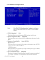
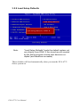
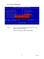
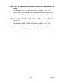
1
PCA-6775
ISA VIA Mark Half-sized SBC
with VGA/LCD/LVDS/10/100
Ethernet/USB and SSD
User Manual
Copyright
This document is copyrighted, © 2007. All rights are reserved. The original manufacturer reserves the right to make improvements to the products
described in this manual at any time without notice.
No part of this manual may be reproduced, copied, translated or transmitted in any form or by any means without the prior written permission of
the original manufacturer. Information provided in this manual is
intended to be accurate and reliable. However, the original manufacturer
assumes no responsibility for its use, nor for any infringements upon the
rights of third parties that may result from such use.
Acknowledgements
Award is a trademark of Award Software International, Inc.
VIA is a trademark of VIA Technologies, Inc.
IBM, PC/AT, PS/2 and VGA are trademarks of International Business
Machines Corporation.
Intel and Pentium are trademarks of Intel Corporation.
Microsoft Windows® is a registered trademark of Microsoft Corp.
RTL is a trademark of Realtek Semi-Conductor Co., Ltd.
ESS is a trademark of ESS Technology, Inc.
UMC is a trademark of United Microelectronics Corporation.
SMI is a trademark of Silicon Motion, Inc.
Creative is a trademark of Creative Technology LTD.
All other product names or trademarks are properties of their respective
owners.
For more information on this and other Advantech products, please visit
our websites at:
http://www.advantech.com
http://www.advantech.com/eplatform
For technical support and service, please visit our support website at:
http://www.advantech.com/support
This manual is for the PCA-6775.
Part No.200K677511
1st Edition
Oct. 2007
PCA-6775 User Manual
ii
Packing List
Before you begin installing your card, please make sure that the following
materials have been shipped:
• 1 PCA-6775 Series Half-sized single board computer
• 1 Startup manual
• 1 CD for utility, drivers, and manual (in PDF format)
• 1 Power cable
p/n:1700000265
• 1 Y cable for PS/2 Keyboard, PS/2 Mouse
p/n:1700060202
• 1 FDD cable (600 mm)
p/n:1701340603
• 1 Printer port cable
p/n:1700260250
• 1 ATX feature cable
p/n:1700001276
• 1 EIDE (HDD) cable
p/n:1701400452
• Mini Jumper
p/n:1653302122
If any of these items are missing or damaged, contact your distributor or
sales representative immediately.
Model No. List
PCA-6775F-L0ALE
Description
ISA VIA Mark 533 MHz Slot SBC
w/1LAN/128 MB on board Memory/LVDS/
CFC
PCA-6775F-Q0A1E
ISA VIA Mark 800 MHz Slot SBC
w/1LAN/LVDS/CFC
PCA-67753F-L0A1E
ISA VIA Mark 533 MHz Slot SBC
w/3LAN/LVDS/CFC
PCA-67753F-Q0A1E
ISA VIA Mark 800 MHz Slot SBC
w/3LAN/LVDS/CFC
iii
Additional Information and Assistance
Visit the Advantech website at www.advantech.com where you can find
the latest information about the product.
Step 1. Contact your distributor, sales representative, or Advantech's customer service center for technical support if you need additional
assistance. Please have the following information ready before
you call:
• Product name and serial number
• Description of your peripheral attachments
• Description of your software (operating system, version, application
software, etc.)
• A complete description of the problem
• The exact wording of any error messages
PCA-6775 User Manual
iv
FCC
This device complies with the requirements in
part 15 of the FCC rules: Operation is subject to
the following two conditions:
1.This device may not cause harmful interference, and
2. This device must accept any interference
received, including interference that may cause
undesired operation
This equipment has been tested and found to
comply with the limits for a Class A digital device,
pursuant to Part 15 of the FCC Rules. These limits are designed to provide reasonable protection
against harmful interference when the equipment
is operated in a commercial environment. This
equipment generates, uses, and can radiate
radio frequency energy and, if not installed and
used in accordance with the instruction manual,
may cause harmful interference to radio communications. Operation of this device in a residential
area is likely to cause harmful interference in
which case the user will be required to correct
the interference at his/her own expense. The
user is advised that any equipment changes or
modifications not expressly approved by the
party responsible for compliance would void the
compliance to FCC regulations and therefore,
the user's authority to operate the equipment.
Caution!
Achtung!
There is a danger of a new battery exploding if it
is incorrectly installed. Do not attempt to
recharge, force open, or heat the battery.
Replace the battery only with the same or equivalent type recommended by the manufacturer.
Discard used batteries according to the manufacturer’s instructions.
v
PCA-6775 User Manual
vi
Contents
Chapter
1 General Information ........................................2
1.3.1
1.3.2
1.3.3
1.3.4
1.3.5
Chapter
2 Installation ........................................................8
2.13.1
2.14.1
2.15.1
2.16.1
2.16.2
2.16.3
2.18.1
2.18.2
2.19.1
2.19.2
2.19.3
Chapter
Table 2.1:Jumpers........................................................... 8
Table 2.2:Connectors ...................................................... 9
CompactFlash (CN23) .................................................. 15
Connecting the floppy drive ......................................... 15
Connecting the hard drive............................................. 16
CRT display Connector (CN15) ................................... 17
LCD panel Connector (CN11,12,13)............................ 17
LCD Inverter Connector (CN8).................................... 17
LAN Connector (CN19) ............................................... 18
Network boot ................................................................ 18
Reset (Pin7&Pin8) ........................................................ 18
HDD LED (Pin1&Pin2,Pin3&Pin4,Pin5&Pin6) .......... 18
Power Button (Pin9&Pin10)......................................... 18
3 BIOS Operation..............................................22
3.2.1
3.2.2
3.2.3
3.2.4
3.2.5
3.2.6
3.2.7
3.2.8
3.2.9
3.2.10
3.2.11
3.2.12
Chapter
Standard SBC Functions................................................. 3
Display Interface............................................................. 3
Solid State disk ............................................................... 3
Ethernet interface............................................................ 3
Mechanical and Environmental ...................................... 4
Main Menu.................................................................... 23
Standard CMOS Features ............................................. 25
Advanced BIOS Features.............................................. 27
Advanced Chipset Features .......................................... 30
Integrated Peripherals ................................................... 34
Power Management Setup ............................................ 38
PnP/PCI Configurations................................................ 40
PC Health Status ........................................................... 41
Load Setup Defaults...................................................... 42
Set Password ................................................................. 43
Save & Exit Setup......................................................... 45
Quit Without Saving ..................................................... 46
4 Driver Installation..........................................48
4.2.1 Step 1- Install VIA INF Update Driver for Windows XP/
2000 ........................................................................... 48
4.2.2 Step 2- Install VIA Graphic Driver for Windows XP
/2000 .......................................................................... 49
4.2.3 Step 3- Install Realtek Ethernet Driver for Windows XP/
2000 ........................................................................... 49
vii
Appendix A Programming GPIO & Watchdog Timer ....52
A.1.1
A.1.2
Appendix B
GPIO Registers ............................................................. 52
GPIO Example program-1 ............................................ 53
Pin Assignments ............................................58
Table B.1:Connector and Jumper Table ....................... 58
Appendix C
System Assignments ......................................72
Table C.1:System I/O ports .......................................... 72
Table C.2:1st MB memory map ................................... 73
Table C.3:DMA channel assignments .......................... 74
Table C.4:Interrupt assignments ................................... 75
PCA-6775 User Manual
viii
CHAPTER
1
General Information
This chapter gives background
information on the PCA-6775.
Sections include:
•
•
•
•
Introduction
Features
Specifications
Board layout and dimensions
1
Chapter 1 General Information
Chapter 1 General Information
1.1 Introduction
The PCA-6775 series is a half-sized ISA bus CPU card designed with
powerful VIA Mark processor, with VIA Mark and 686B chipset, which
supports integrated graphic. For maximum performance, PCA-6775 also
supports one 144 Pin SODIMM socket and SDRAM memory up to 512
MB.
Other onboard features include 1 EIDE, 1 FDD, 1 LPT, 4 USB 1.1, 2
COM ports (1 x RS-232 and 1 x RS-232/422/485), PS/2 KeyBoard/
mouse, watchdog, and a DI/O interface. The SSD solution supports Type
I/II CompactFlash cards.
This product uses a VIA Mark that supports VGA/LVDS interface, 2
channel (36-bit) LVDS LCD panel. PCA-6775 supports AC97 audio with
the addition of the optional PCM-231A-00A1E audio module.
The Ethernet interface supports 10/100Base-T by Realtek 8100C. Its
dimension follows standard ISA slot PC, this makes it can match with all
half-sized chassis and can operate in high vibration environment.
1.2 Features
• VIA Mark 533/800 MHz processor
• Fanless operation at 0 ~ 60° C
• On-board VGA/LVDS display
• Supports 100Base-T Ethernet on board
• Supports 4 x USB 1.1 ports
• Supports 2 Channel 36-bit LVDS for LCD
• Supports 133 MHz Front Side Bus
• Accepts PC-100/133 SDRAM
PCA-6775 User Manual
2
1.3 Specifications
1.3.1 Standard SBC Functions
• CPU: VIA Mark 533/800 MHz processor
• System chipsets: VIA Mark + 686B
• BIOS: Award 4Mbit Flash BIOS
• System memory: 144 pin SODIMMx1, supports 128 MB to 512 MB,
accepts PC-100/133 SDRAM
• 2nd cache memory: 64 KB
• Enhanced IDE Interface: Supports two enhanced IDE channels. Primary channel supports ATA-100 mode; Secondary channel only
supports ATA-33 and PIO mode. CFC card occupies secondary IDE
master
• COM Ports: Two COM ports: COM1: RS-232; COM2: RS-232/422/
485
• Printer Ports: One printer port, support SPP/EPP/ECP
• Keyboard/Mouse Connector: Supports standard PC/AT Keyboard and
a PS/2 Mouse
• Power Management: Supports Power Saving Mode, including Normal/
Standard/Suspend modes. APM 1.2 compliant.
• FDD interface: Supports up to one FDD devices
• DI/O interface: 8-bit general purpose input/output
• Watchdog Timer: 0 ~ 255 Sec. System reset or IRQ11
• Expansion Interface: 16-bit ISA Slot
• Battery: Lithium 3V/196 mAH
• USB: 4 USB ports, USB 1.1 compliant
1.3.2 Display Interface
• Chipset: VIA Mark
• Memory size: Shared up to 32 MB
• LVDS Interface: Supports 2 channel (36-bit) LVDS LCD Panel
• Display modes:
CRT Modes: 1920 x 1440 @ 85 Hz;
LCD Modes: up to UXGA panel resolution with
frequency range from 25 MHz to 112 MHz
1.3.3 Solid State disk
• Supports CompactFlash Card Type I/II
1.3.4 Ethernet interface
• Chipset: Realtek 8100C 10/100Mbps Lan Chip
• Connection: on-board RJ-45 connector
• Interface: IEEE 802.3u (100Base-T) protocol compatible
3
Chapter 1 General Information
• Built-in Boot ROM: 8100C
• I/O address switchless setting
1.3.5 Mechanical and Environmental
• Dimensions (L x W): 185 x 122 mm (7.3” x 4.8”)
• Power Supply Voltage:+5 V ± 5%, +12 V ± 5%
• Power Consumption:
Max:
+5 V @ 2.20 A, +12 V @ 0.04 A
Typical:
+5 V @ 1.64 A, +12 V @ 0.01 A
(VIA Mark 533 MHz with 256 MB SDRAM)
• Operating temperature: 0 ~ 60° C (32 ~ 140° F) operation
• Operating humidity: 0% ~ 90% Relative Humidity, non-condensing
PCA-6775 User Manual
4
180.99
183.14
172.02
141.86
148.45
151.64
158.37
161.99
162.56
97.35
98.89
77.66
77.73
85.41
51.69
3.01
7.88
8.26
8.38
11.69
16.52
18.23
25.69
45.25
1.4 Board layout: dimensions
119.84
119.59
117.99
116.01
113.91
111.46
104.71
118.70
118.32
118.05
117.43
114.83
107.31
104.77
98.99
98.10
97.66
98.10
96.35
95.97
70.82
60.56
46.28
45.55
45.55
32.72
26.85
23.55
19.51
18.62
16.21
9.27
159.18
170.05
173.32
177.18
177.70
178.17
148.85
101.60
103.89
107.57
77.73
45.47
16.52
0.00
3.01
0.00
178.65
178.99
124.89
127.51
75.73
82.11
84.73
89.25
14.52
1.01
Figure 1.1: Board layout: dimensions (component side)
118.05
117.99
103.50
96.35
94.58
79.08
78.40
70.88
63.33
50.63
45.55
21.16
19.51
178.71
77.72
78.87
15.87
16.52
0.00
3.01
0.00
Figure 1.2: Board layout: dimensions (solder side)
5
Chapter 1 General Information
PCA-6775 User Manual
6
CHAPTER
2
Installation
This chapter explains the setup procedures
of PCA-6775 hardware, including instructions on setting jumpers and connecting
peripherals, switches and indicators. Be
sure to read all safety precautions before
you begin the installation procedure.
7
Chapter 2 Installation
Chapter 2 Installation
2.1 Jumpers
The PCA-6775 has a number of jumpers that allow you to configure your
system to suit your application. The table below lists the functions of the
various jumpers.
Table 2.1: Jumpers
Label
Function
J1
LVDS Panel Power Select
J2
COM2 function selection
J3
AT power selection
J4
Clear CMOS Jumper
PCA-6775 User Manual
8
2.2 Connectors
Onboard connectors link the PCA-6775 to external devices such as hard
disk drives, a keyboard, or floppy drives. The table below lists the function of each of the board’s connectors.
Table 2.2: Connectors
Label
Function
CN1
System FAN connector
CN2
ATX Power Connector
CN3
Printer port Connector
CN4
Floppy disk device Connector
CN5
Primary IDE Connector
CN6
Front panel Connector
CN7
Digital I/O Connector
CN8
LCD inverter board Connector
CN9
ATX Power Connector
CN10
Secondary IDE Connector
CN11
LVDS Connector
CN12
LCD (24~35-bit) Connector
CN13
LCD (0~23-bit) Connector
CN14
AC97 Connector
CN15
VGA Connector
CN16
Universal Series Bus Connector1/2
CN17
Universal Series Bus Connector3/4
CN18
Power input Connector
CN19
LAN * 3 Connector
CN21
COM1 Connector
CN22
COM2 Connector (share with RS422 , RS485)
CN23
Extend Keyboard and Mouse Connector
CN24
Keyboard and Mouse Connector
CN25
Compact Flash Card Connector
CN26
Memory Connector SODIMM
9
Chapter 2 Installation
2.3 Locating Connectors (component side)
Figure 2.1: Jumper & Connector Locations
2.4 Locating Connectors (solder side)
Figure 2.2: Connectors (component side)
PCA-6775 User Manual
10
2.5 Setting Jumpers
You may configure your card to match the needs of your application by
setting jumpers. A jumper is a metal bridge used to close an electric circuit. It consists of two metal pins and a small metal clip (often protected
by a plastic cover) that slides over the pins to connect them. To “close” a
jumper, you connect the pins with the clip. To “open” a jumper, you
remove the clip. Sometimes a jumper will have three pins, labeled 1, 2
and 3. In this case you would connect either pins 1 and 2, or 2 and 3.
open
closed
closed 2-3
The jumper settings are schematically depicted in this manual as follows:.
open
closed
closed 2-3
A pair of needle-nose pliers may be helpful when working with jumpers.
If you have any doubts about the best hardware configuration for your
application, contact your local distributor or sales representative before
you make any changes. Generally, you simply need a standard cable to
make most connections.
11
Chapter 2 Installation
2.6 Clear CMOS (J4)
Warning!
To avoid damaging the computer, always turn
off the power supply before setting “Clear
CMOS.” Before turning on the power supply,
set the jumper back to “3.0 V Battery On.”
This jumper is used to erase CMOS data and reset system BIOS information.
The procedure for clearing CMOS is:
1.
Turn off the system.
2.
Short pin 1 and pin 2.
3.
Turn on the system. The BIOS is now reset to its default setting
Table 2.3:
Clear CMOS (JP1)
Clear CMOS
PCA-6775 User Manual
12
2.7 COM2 RS-232/422/485 Select (J2)
Table 2.4: COM2 RS-232/422/485 Select
1-2 (default)
RS-232
3-4
RS-422
5-6
RS-485
2.8 AT Power select (J3)
1
2
3
1
2
3
Table 2.5: AT Power select
Pin
Function
1-2 (default)
AT power
2-3
No Active
2.9 LVDS Panel Power Select (J1)
1
2
3
1
2
3
Table 2.6: LVDS Panel Power Select
Pin
Function
1-2 (default)
+5 V
2-3
+3.3 V
13
Chapter 2 Installation
2.10 Installing SODIMMs
Notes
The modules can only fit into a socket one way.
The gold pins must point down into the
SODIMM socket.
The procedure for installing SODIMMs appears below. Please follow
these steps carefully.
1. Make sure that all power supplies to the system are switched off
2. Install the SODIMM card. Install the SODIMM so that its gold pins
point down into the SODIMM socket.
3. Slip the SODIMM into the socket at a 45 degree angle and carefully fit the bottom of the card against the connectors.
4. Gently push the SODIMM into a perpendicular position until the
clips on the ends of the SODIMM sockets snap into place.
5. Check to ensure that the SODIMM is correctly seated and all connector contacts touch. The SODIMM should not move around in its
socket.
2.11 ATX power control Connector (CN5)
The PCA-6775 supports ATX power. CN5 supplies main power (+5 V ,
+12 V , 5 VSB), and it is a 6 x 2 pins power connector, w/Fixed Lock
4200-WS-A1.
Important
Make sure that the ATX power supply can take
at least a 10 mA load on the 5 V standby lead
(5 VSB). If not, you may have difficulty powering on your system.
PCA-6775 User Manual
14
2.12 Printer port Connector (CN3)
Normally, the printer port is used to connect the card to a printer. The
PCA-6775 includes a multi-mode (SPP/EPP/ECP) printer port accessed
via CN3 and a 26-pin flat-cable connector. You will need an adapter cable
if you use a traditional DB-25 connector. The adapter cable has a 26-pin
connector on one end, and a DB-25 connector on the other.
The printer port is designated as LPT1, and can be disabled or changed to
LPT2 or LPT3 in the system BIOS setup.
The printer port interrupt channel is designated to be IRQ7.
You can select ECP/EPP DMA channel via BIOS setup.
2.13 CompactFlash Socket
The PCA-6775 provides a 50-pin socket for CompactFlash card type I/II.
2.13.1 CompactFlash (CN23)
The CompactFlash card occupies a secondary IDE channel which can be
enabled/disabled via the BIOS settings.
2.14 Floppy Connector (CN4)
You can attach up to two floppy drives to the PCA-6775’s on-board controller. You can use any combination of 5.25” (360 KB and 1.2 MB) and/
or 3.5” (720 KB, 1.44 MB, and 2.88 MB) drives.
A 34-pin daisy-chain drive connector cable is required for a dual-drive
system. On one end of the cable is a 34-pin flat-cable connector. On the
other end are two sets of floppy disk drive connectors. Each set consists
of a 34-pin flat-cable connector (usually used for 3.5” drives) and a
printed-circuit board connector (usually used for 5.25” drives).
2.14.1 Connecting the floppy drive
1.
Plug the 34-pin flat-cable connector into CN4. Make sure that the
red wire corresponds to pin one on the connector.
2.
Attach the appropriate connector on the other end of the cable to
the floppy drive(s). You can use only one connector in the set. The
set on the end (after the twist in the cable) connects to the A: drive.
The set in the middle connects to the B: drive.
15
Chapter 2 Installation
3.
If you are connecting a 5.25” floppy drive, line up the slot in the
printed circuit board with the blocked-off part of the cable connector.
If you are connecting a 3.5” floppy drive, you may have trouble determining which pin is number one. Look for a number printed on the circuit
board indicating pin number one. In addition, the connector on the floppy
drive may have a slot. When the slot is up, pin number one should be on
the right. Check the documentation that came with the drive for more
information.
If you desire, connect the B: drive to the connectors in the middle of the
cable as described above.
In case you need to make your own cable, you can find the pin assignments for the board’s connector in Appendix B.
2.15 IDE Connector (CN5,CN10)
The PCA-6775 provides two IDE channels to which you can attach up to
four Enhanced Integrated Device Electronics hard disk drives or
CDROM to the PCA-6775’s internal controller. The PCA-6775’s IDE
controller uses a PCI interface. This advanced IDE controller supports
faster data transfer, PIO Mode 3 or Mode 4, UDMA 33/66/100 mode.
2.15.1 Connecting the hard drive
Connecting drives is done in a daisy-chain fashion. It requires one of two
cables (not included in this package), depending on the drive size. 1.8"
and 2.5" drives need a 1 x 44-pin to 2 x 44-pin flat-cable connector. 3.5"
drives use a 1 x 44-pin to 2 x 40-pin connector.
Wire number 1 on the cable is red or blue, and the other wires are gray.
1.
Connect one end of the cable to CN5,CN10. Make sure that the red
(or blue) wire corresponds to pin 1 on the connector, which is
labeled on the board (on the right side).
2.
Plug the other end of the cable into the Enhanced IDE hard drive,
with pin 1 on the cable corresponding to pin 1 on the hard drive.
(See your hard drive’s documentation for the location of the connector.)
If desired, connect a second drive as described above.
Unlike floppy drives, IDE hard drives can connect to either end of the
cable. If you install two drives, you will need to set one as the master and
one as the slave by using jumpers on the drives. If you install only one
drive, set it as the master.
PCA-6775 User Manual
16
2.16 VGA/LVDS interface connections
The PCA-6775’s display interface can drive conventional CRT displays
and is capable of driving a wide range of LVDS flat panel displays as
well. The board has two display connectors: one for standard CRT VGA
monitors, and one for LVDS flat panel displays.
2.16.1 CRT display Connector (CN15)
CN10 is a standard 15-pin D-SUB connector used for conventional CRT
displays. Users can drive a standard progressive scan analog monitor with
pixel resolution up to 2048 x 1536 at 75 Hz. Pin assignments for CRT display connector CN10 are detailed in Appendix B.
2.16.2 LCD panel Connector (CN11,12,13)
PCA-6775 uses the VIA Mark to supports single or dual-channel LVDS
panels up to UXGA panel resolution with frequency range from 25MHz
to 112MHz.
The display mode can be 2 channels (2 x 18 bits) LVDS LCD panel displays Users can connect to either an 18, 24 or 36 bits LVDS LCD with
CN11 and connect to TTL LCD with CN12,13.
2.16.3 LCD Inverter Connector (CN8)
The LCD inverter is connected to CN8 via a 5-pin connector to provide
+5 V/+12 V power to the LCD display.
2.17 USB Connectors (CN16,CN17)
The PCA-6775 board provides up to four USB (Universal Serial Bus)
ports. This gives complete Plug and Play, and hot attach/detach for up to
127 external devices. The USB interfaces comply with USB specification
Rev. 2.0, and are fuse protected.
The USB interface is accessed through the 5 x 2-pin flat-cable connector,
CN16 (USB1, 2),CN17 (USB3, 4). You will need an adapter cable if you
use a standard USB connector. The adapter cable has a 5 x 2-pin connector on one end and a USB connector on the other.
The USB interfaces can be disabled in the system BIOS setup.
17
Chapter 2 Installation
2.18 Ethernet Configuration
The PCA-6775 is equipped with a high performance 32-bit PCI-bus
Ethernet interface which is fully compliant with IEEE 802.3u 10/
100Mbps CSMA/CD standards. It is supported by all major network
operating systems.
The PCA-6775 supports 10/100Base-T Ethernet connections with
onboard RJ-45 connectors (CN19).
2.18.1 LAN Connector (CN19)
10/100Base-T or 1000Base-T connects to the PCA-6775 via a cable to a
standard RJ-45 connector.
2.18.2 Network boot
The Network Boot feature can be utilized by incorporating the Boot
ROM image files for the appropriate network operating system. The Boot
ROM BIOS files are included in the system BIOS, which is on the utility
CD disc.
2.19 HDD LED/Reset/Power Button (CN6)
Next, you may want to install external switches to monitor and control the
PCA-6775. These features are optional: install them only if you need
them. CN6 is an 2 x 5 pin header, 180 degree, male. It provides connections for reset and power & hard disk indicator.
2.19.1 Reset (Pin7&Pin8)
If you install a reset switch, it should be an open single pole switch.
Momentarily pressing the switch will activate a reset. The switch should
be rated for 10 mA, 5 V.
2.19.2 HDD LED (Pin1&Pin2,Pin3&Pin4,Pin5&Pin6)
The HDD LED indicator for hard disk access is an active low signal (24
mA sink rate).
Pin3&Pin4
The HDD LED indicator would light when the power is on.
Pin5&Pin6
The HDD LED indicator would light when the computer is suspend.
2.19.3 Power Button (Pin9&Pin10)
PCA-6775 also supports power on/off button.
PCA-6775 User Manual
18
2.20 COM port Connector (CN21, CN22)
The PCA-6775 provides two COM ports (COM1: RS-232 and COM2:
RS-232/422/485). CN21 supports COM1, CN22 supports COM2. And J2
is for COM2 RS-232/422/485 selection. It provides connections for serial
devices (a mouse, etc.) or a communication network. You can find the pin
assignments for the COM port connector in Appendix B.
2.21 MINI Keyboard Connector (CN24)
The PCA-6775 board provides a keyboard connector that supports both a
keyboard and a PS/2 style mouse. In most cases, especially in embedded
applications, a keyboard is not used. If the keyboard is not present, the
standard PC/AT BIOS will report an error or fail during power-on selftest (POST) after a reset. The PCA-6775’s BIOS standard setup menu
allows you to select “All, But Keyboard” under the “Halt On” selection.
This allows no-keyboard operation in embedded system applications,
without the system halting under POST.
2.22 External Keyboard Connector (CN23)
In addition to the Mini keyboard connector on the PCA-6775’s rear plate,
there is an additional onboard external keyboard connector, allowing for
greater flexibility in system design.
2.23 Audio Interface Connector (CN14)
The Audio Interface link is a 10 pin connector, the PCA-6775 can support
Audio with the addition of optional PCM-231A-00A1. Detailed pin
assignment refer to Appendix B.
2.24 DI/O Connector (CN7)
The PCA-6775 supports DI/O interface by CN7, which is a 7 x 2 dual line
pin header, supply 8-bit general purpose input or output ports.
19
Chapter 2 Installation
PCA-6775 User Manual
20
CHAPTER
3
BIOS Operation
This chapter describes how to set BIOS
configuration data.
Chapter 3 BIOS Operation
3.1 BIOS Introduction
Advantech provide full-featured AwardBIOS 6.0 and delivers the superior performance, compatibility and functionality that manufactures of
Industry PC and Embedded boards, it’s many options and extensions let
you customize your products to a wide range of designs and target markets.
The modular, adaptable AwardBIOS 6.0 supports the broadest range of
third-party peripherals and all popular chipsets, plus Intel, AMD, nVidia,
VIA, and compatible CPUs from 386 through Pentium and AMD Geode,
K7 and K8 (including multiple processor platforms), and VIA Eden C3
and C7 CPU.
You can use Advantech’s utilities to select and install features to suit your
designs for customers need.
3.2 BIOS Setup
The PCA-6775 Series system has build-in AwardBIOS with a CMOS
SETUP utility which allows user to configure required settings or to activate certain system features.
The CMOS SETUP saves the configuration in the CMOS RAM of the
motherboard. When the power is turned off, the battery on the board supplies the necessary power to the CMOS RAM.
When the power is turned on, press the <Del> button during the BIOS
POST (Power-On Self Test) will take you to the CMOS SETUP screen.
CONTROL KEYS
< ↑ >< ↓ >
< ← >< → >
Move to select item
<Enter>
<Esc>
Select Item
Main Menu - Quit and not save changes into CMOS
Sub Menu - Exit current page and return to Main Menu
Increase the numeric value or make changes
Decrease the numeric value or make changes
General help, for Setup Sub Menu
Item Help
<Page Up/+>
<Page Down/->
<F1>
<F2>
PCA-6775 User Manual
22
<F5>
<F7>
<F10>
Load Previous Values
Load Optimized Default
Save all CMOS changes
3.2.1 Main Menu
Press <Del> to enter AwardBIOS CMOS Setup Utility, the Main Menu
will appear on the screen. Use arrow keys to select among the items and
press <Enter> to accept or enter the sub-menu.
• Standard CMOS Features
This setup page includes all the items in standard compatible BIOS.
• Advanced BIOS Features
This setup page includes all the items of Award BIOS enhanced features.
• Advanced Chipset Features
This setup page includes all the items of Chipset configuration features.
• Integrated Peripherals
This setup page includes all onboard peripheral devices.
• Power Management Setup
This setup page includes all the items of Power Management features.
23
Chapter 3
• PnP/PCI Configurations
This setup page includes PnP OS and PCI device configuration.
• PC Health Status
This setup page includes the system auto detect CPU and system temperature, voltage, fan speed.
• Load Setup Defaults
This setup page includes Load system optimized value, and the system
would be in best performance configuration.
• Set Password
Establish, change or disable password.
• Save & Exit Setup
Save CMOS value settings to CMOS and exit BIOS setup.
• Exit Without Saving
Abandon all CMOS value changes and exit BIOS setup.
PCA-6775 User Manual
24
3.2.2 Standard CMOS Features
• Date
The date format is <week>, <month>, <day>, <year>.
Week
From Sun to Sat, determined and display by BIOS only
Month From Jan to Dec.
Day
From 1 to 31
Year
From 1999 through 2098
• Time
The times format in <hour> <minute> <second>, base on the 24-hour
time
• IDE Primary Master
IDE HDD Auto-Detection Press “Enter” for automatic device detection.
• IDE Primary Slave
IDE HDD Auto-Detection Press “Enter” for automatic device detection.
• IDE Secondary Master
IDE HDD Auto-Detection Press “Enter” for automatic device detection.
• IDE Secondary Slave
IDE HDD Auto-Detection Press “Enter” for automatic device detection.
25
Chapter 3
• Drive A / Drive B
The Item identifies the types of floppy disk drive A or drive B
None
No floppy drive installed
360K, 5.25" 5.25 inch PC-type standard drive; 360K byte capacity
1.2M, 5.25" 5.25 inch AT-type high-density drive; 1.2M byte capacity
720K, 3.5"
3.5 inch double-sided drive; 720K byte capacity
1.44M, 3.5" 3.5 inch double-sided drive; 1.44M byte capacity
2.88M, 3.5" 3.5 inch double-sided drive; 2.88M byte capacity
• Video
The item determines that VGA display support type.
EGA/VGASupport VGA color mode.
CGA 40 Support VGA color mode.
CGA 80 Support VGA color mode.
MONO
Support VGA mono mode.
• Halt on
The item determines whether the computer will stop if an error is
detected during power up.
No Errors
The system boot will not stop for any error
All Errors
Whenever the BIOS detects a non-fatal error the
system will be stopped.
All, But Keyboard
The system boot will not stop for a keyboard
error; it will stop for all other errors. (Default
value)
All, But Diskette
The system boot will not stop for a disk error; it
will stop for all other errors.
All, But Disk/Key
The system boot will not stop for a keyboard or
disk error; it will stop for al other errors.
• Base Memory
The POST of the BIOS will determine the amount of base (or conventional) memory installed in the system.
• Extended Memory
The POST of the BIOS will determine the amount of extended memory
(above 1 MB in CPU’s memory address map) installed in the system.
PCA-6775 User Manual
26
• Total Memory
This item displays the total system memory size.
3.2.3 Advanced BIOS Features
• Virus Warning
[Disabled]
This item allows user to choose the VIRUS Warning feature for IDE
Hard Disk boot sector protection.
• CPU Internal Cache
[Enabled]
This item allows user to enable CPU internal cache.
• CPU L2 Cache ECC Checking
[Enabled]
This item allows user to enable CPU L2 cache and ECC checking
function.
• Quick Power On Self Test
[Enabled]
This field speeds up the Power-On Self Test (POST) routine by skipping retesting a second, third and forth time. Setup setting default is
“enabled”.
27
Chapter 3
• First / Second / Third / Other Boot Drive
Floppy
Select boot device priority by Floppy.
LS120
Select boot device priority by LS120.
Hard Disk
Select boot device priority by Hard Disk.
CDROM
Select boot device priority by CDROM.
ZIP
Select boot device priority by ZIP.
USB-FDD
Select boot device priority by USB-FDD.
USB-ZIP
Select boot device priority by USB-ZIP.
USB-CDROM
Select boot device priority by USB-CDROM.
USB-HDD
Select boot device priority by USB-HDD.
LAN
Select boot device priority by LAN.
Disabled
Disable this boot function.
• Swap Floppy Drive
[Disabled]
This item enables users to swap floppy “A” and “B” identified without
change hardware cable connection.
• Boot Up Floppy Seek
[Enabled]
When enabled, the BIOS will seek the floppy “A” drive one time
• Boot Up NumLock Status
[On]
This item enables users to activate the Number Lock function upon
system boot
• Typematic Rate Setting
[Disabled]
This item enables users to set the two typematic controls items.
This field controls the speed at
- Typematic Rate (Chars/Sec)
This item controls the speed at system registers repeated keystrokes.
Eight settings are 6, 8, 10, 12, 15, 20, 24 and 30.
- Typematic Delay (Msec)
This item sets the time interval for displaying the first and second
characters. Four delay rate options are 250, 500, 750 and 1000.
PCA-6775 User Manual
28
• Security Option[Setup]
System
System can not boot and can not access to Setup page if the
correct password is not entered at the prompt.
Setup
System will boot, but access to Setup if the correct password
is not entered at the prompt. (Default value)
• OS Select For DRAM > 64M
[Non-OS2]
Select OS2 only if system is running OS/2 operation system with
greater than 64 MB of RAM on the system.
• Video BIOS Shadow[Enabled]
Enabled copies Video BIOS to shadow RAM improves performance.
- C8000-CBFFF Shadow [Disabled]
It’s for shadow control of item.
- CC000-CFFFF Shadow [Disabled]
It’s for shadow control of item.
- D0000-D3FFF Shadow [Disabled]
It’s for shadow control of item.
- D4000-D7FFF Shadow [Disabled]
It’s for shadow control of item.
- D8000-DBFFF Shadow[ Disabled]
It’s for shadow control of item.
- DC000-DFFFF Shadow [Disabled]
• Small Logo (EPA) Show
[Enabled]
Show EPA logo during system post stage.
29
Chapter 3
3.2.4 Advanced Chipset Features
Note:
This “Advanced Chipset Features” option controls
the configuration of the board’s chipset, this page is
developed by Chipset independent, for control
chipset register setting and fine tune system performance. It is strongly recommended only technical
users make changes to the default settings.
• DRAM Timing By SPD
[Enabled]
This item is use DRAM of default setting or not. User can choose disabled to modify different of DRAM setting.
• DRAM Clock
[Host CLK]
This item is standard DRAM clock or not. User could use different setting to modify DRAM clock.
• SDRAM Cycle Length
[3]
This item is control DRAM clock cycle of length, User can use it to
changed different clock cycle length.
• Bank Interleave
[Disabled]
This item is support DRAM interleaving technology. Enabled bank
interleave can save time and improvement data transmission rate.
PCA-6775 User Manual
30
• Memory Hole [Disabled]
This item reserves 15 MB-16 MB memory address space to ISA
expansion cards that specifically require the setting. Memory from 15
MB-16 MB will be unavailable to the system because of the expansion
cards can only access memory at this area.
• P2C/C2P Concurrency [Enabled]
This item is enable PCI bus access speed, P2C/C2P menus that PCI to
CPU/CPU to PCI. BIOS default suggest to enabled.
• System BIOS Cacheable
[Enabled]
This item allows the system BIOS to be cached to allow faster execution and better performance.
• Video BIOS Cacheable
[Disabled]
This item allows the video BIOS to be cached to allow faster execution
and better performance.
• Frame Buffer Size
[16M]
This item enables users to set Video Memory size, system default is
setting to “32 MB” to reference value.
• AGP Aperture Size
[64M]
This item enables users to select size of system memory to support
AGP graphic usage, system default is setting to “64 MB” to reference
value.
• AGP-4X Mode
[Enabled]
This item is supports the AGP 4X transfer protocol, The AGP 4X protocol must be supported by both the motherboard and graphics card for
this feature to work.
• AGP Driving Control
[Enabled]
This item is supports the AGP Driving force, BIOS default setting is
enable to automatic pick one value for booting. If you have troubleshooting or overclocking purpose, You can chose option by Manual.
• AGP Driving Value
[DA]
This item could to adjust AGP Driving force for troubleshooting or overclocking purpose. User set value range from “00” to “FF”.
• Select Display Device
[Auto]
This item is provided output screen type selection. BIOS default value
suggest to “Auto”.
31
Chapter 3
• Panel Type
[TFT 800*600 18 bit]
This item is provided LCD panel resolution type selection. BIOS
default value suggest to “TFT 800*600 18 bit”.
• Onboard Lan1
[Enabled]
This item is controller to enabled or disabled motherboard of Lan1
device.
• Onboard Lan2
[Enabled]
This item is controller to enabled or disabled motherboard of Lan2
device.
• Onboard Lan3
[Enabled]
This item is controller to enabled or disabled motherboard of Lan3
device.
• OnChip USB
[Enabled]
This item is controller to enabled or disabled motherboard of USB controller.
• USBKeyboard Support
[Disabled]
This item is controller to enabled or disabled of USB keyboard under
DOS/Legacy environment.
• OnChip Sound
[Auto]
This item is controller to enabled or disabled motherboard of sound
device.
• OnChip Modem
[Auto]
This item is controller to enabled or disabled motherboard of modem
device.
• CPU to PCI Write Buffer
[Enabled]
This item is enabled or disabled PCI write buffer for CPU, If disable
buffer, It will directly write data from CPU to PCI, Although look like the
faster, But CPU bus is fast than the PCI bus, CPU bus must to waiting for
PCI bus ready for receive next data. So BIOS default value suggest to
“Enabled”.
• PCI Dynamic Bursting[Enabled]
This item is enabled or disabled PCI write buffer of bandwidth, If enabled
this item, PCI bus will used 32-bit data write access. For good efficiency,
BIOS default value suggest to “Enabled”.
PCA-6775 User Manual
32
• PCI Master 0 WS Write
[Enabled]
This item is enabled or disabled PCI master wait state, PCI bus will
write immediately when set to enable. For good efficiency, BIOS
default value suggest to “Enabled”.
• PCI Delay Transaction
[Disabled]
This item is enabled or disabled PCI Data Delay Transaction. The PCI
device must to meet the PCI 2.1 compliant of target latency rule. BIOS
default value suggest to “Disabled”.
• PCI#2 Access #1 Retry
[Enabled]
This item allows enabled or disabled that CPU to PCI write buffer. It
will reattempt to write to PCI bus until successful. BIOS default value
suggest to “Enabled”.
• AGP master 1 WS Write
[Enabled]
This item allows enabled or disabled that single delay write form AGP
bus. BIOS default value suggest to “Enabled”.
• AGP master 1 WS read
[Enabled]
This item allows enabled or disabled that single delay read form AGP
bus. BIOS default value suggest to “Enabled”.
33
Chapter 3
3.2.5 Integrated Peripherals
Note:
This “Integrated Peripherals” option controls the configuration of the board’s chipset, includes IDE, ATA,
SATA, USB, AC97, MC97 and Super IO and Sensor
devices, this page is developed by Chipset independent.
• OnChip IDE Channel0
This item enables chipset IDE device 0 of controller.
• OnChip IDE Channel1
This item enables chipset IDE device 1 of controller.
• IDE Prefetch Mode[Enabled]
This item allows enabled or disabled that IDE controller prefetch data
from the IDE driver. BIOS default value suggest to “Enabled”.
• Primary Master PIO[Auto]
This item allows user to adjust primary master IDE mode of type for
modification purpose. BIOS default value suggest to “Auto”.
• Primary Slave PIO[Auto]
This item allows user to adjust primary slave IDE mode of type for
modification purpose. BIOS default value suggest to “Auto”.
PCA-6775 User Manual
34
• Secondary Master PIO[Auto]
This item allows user to adjust secondary master IDE mode of type for
modification purpose. BIOS default value suggest to “Auto”.
• Secondary Slave PIO[Auto]
This item allows user to adjust secondary slave IDE mode of type for
modification purpose. BIOS default value suggest to “Auto”.
• Primary Master UDMA[Auto]
This item allows user to adjust primary master IDE mode of type for
modification purpose. BIOS default value suggest to “Auto”.
• Primary Slave UDMA[Auto]
This item allows user to adjust primary slave IDE mode of type for
modification purpose. BIOS default value suggest to “Auto”.
• Secondary Master UDMA[Auto]
This item allows user to adjust secondary master IDE mode of type for
modification purpose. BIOS default value suggest to “Auto”.
• Secondary Slave UDMA[Auto]
This item allows user to adjust secondary slave IDE mode of type for
modification purpose. BIOS default value suggest to “Auto”.
• Init Display First[PCI]
This item allows user to changed display card of adapter. BIOS default
value suggest to “PCI”.
• SATA Mode
[BASE(non-RAID)]
This item allows user to changed SATA mode. BIOS default value suggest to “BASE(non-RAID)”.
• IDE HDD Block Mode
[Enabled]
This item allows enabled or disabled that IDE block data transfer
mode. It will speed up HDD data transfer of efficiency. BIOS default
value suggest to “Enabled”.
• Onboard FDD Controller
[Enabled]
This item allows user to enabled or disabled chipset FDD controller.
BIOS default value suggest to “Enabled”.
• Onboard Serial Port 1
[3F8/IRQ4]
This item allows user to change com1 port of address. BIOS default
value suggest to “3F8/IRQ4”.
35
Chapter 3
• Onboard Serial Port 2
[2F8/IRQ3]
This item allows user to change COM2 port of address. BIOS default
value suggest to “2F8/IRQ3”.
• UART 2 Mode
[Standard]
This item allows user to change COM2 port of transmission protocol.
BIOS default value suggest to “Standard”.
• IR Function Duplex
[Half]
This item is default to show only. Except user to change item “UART 2
Mode” with another mode. BIOS default value suggest to “Half”.
• TX,RX Inverting Enable
[No, Yes]
This item is default to show only. Except user to change item “UART 2
Mode” with another mode. BIOS default value suggest to “No, Yes”.
• Onboard Parallel Port
[378/IRQ7]
This item allows user to change parallel port of address. BIOS default
value suggest to “378/IRQ7”.
• Onboard Parallel Mode
[Normal]
This item allows user to change parallel port of mode. User can choose
“EPP”, “ECP” and “ECP+EPP”. ECP(Extended Capabilities Port).
EPP(Enhanced Parallel Port). BIOS default value suggest to “Normal”.
• ECP Mode Use DMA
[3]
This item allows user to change DMA channel for parallel port. BIOS
default value suggest to “3”.
• Parallel Port EPP Type
[EPP1.9]
This item allows user to change EPP mode of version. BIOS default
value suggest to “EPP1.9”.
• Onboard Legacy Audio
[Enabled]
This item is enabled or disabled that onboard of audio controller. BIOS
default value suggest to “Enabled”.
• Sound Blaster
[Disable]
This item is enabled or disabled that onboard of sound blaster controller. BIOS default value suggest to”Disabled”.
• SB I/O Base Address
[220H]
This item allows user to change different address for sound blaster.
BIOS default value suggest to “220H”.
PCA-6775 User Manual
36
• SB IRQ Select
[IRQ 5]
This item allows user to change different IRQ for sound blaster. BIOS
default value suggest to “IRQ 5”.
• SB DMA Select
[DMA 1]
This item allows user to change different DMA for sound blaster.
BIOS default value suggest to “DMA 1”.
• MPU-401
[Disable]
This item allows user to control that compatible MIDI interface. BIOS
default value suggest to “Disabled”.
• MPU-401 I/O Address
[330-333H]
This item allows user to change that compatible MIDI interface
address. BIOS default value suggest to “330-333H”.
• Game Port (200-207H)
[Enabled]
This item allows user to enabled or disabled that decode game port
address. BIOS default value suggest to “Enabled”.
37
Chapter 3
3.2.6 Power Management Setup
Note:
This “Power management Setup” option configure
system to most effectively saving energy while operating in a manner consistent with your computer use
style.
• ACPI Function
[Enabled]
This item defines the ACPI (Advanced Configuration and Power Management) feature that makes hardware status information available to
the operating system, and communicate PC and system devices for
improving the power management.
• Power Management
[Press Enter[
This item allows user to select system power saving mode.
Power management
[User Define]
User Define Allows user to set each mode individually. Suspend
Mode= Disabled or 1 min ~ 1 hr.
Min Saving Minimum power management. Suspend Mode = 1 hr.
Max Saving Maximum power management. Suspend Mode = 1
min.
HDD Power Down
PCA-6775 User Manual
[Disable]
38
It could change HDD power down suspend range from 1 Min to 15
Min.
Doze Mode
[Disable]
It could change system Doze mode range from 1 Min to 1hour.
Suspend Mode
[Disable]
It could change system suspend mode range from 1 Min to 1hour.
• PM Control by APM
[YES]
This item allows user to determine power management control by
APM function or not.
• Video Off Option
[Suspend -> off]
This item allows user to turn off Video during system enter suspend
mode.
• Video Off Method
[DPMS]
This item allows user to determine the manner is which the monitor is
blanked.
V/H SYNC+Blank This option will cause system to turn off vertical
and horizontal synchronization ports and write
blanks to the video buffer.
Blank Screen
This option only writes blanks to the video buffer.
DPMS
Initial display power management signaling.
• Modem use IRQ
[3]
This item allows user to determine the IRQ which the MODEM can
use.
• Soft-Off by PWR-BTTN
[Enabled]
This item allows user to define function of power button.
Instant-Off
Press power button then Power off instantly.
Delay 4 Sec
Press power button 4 sec. to Power off.
• Wake-Up Events
[Press Enter]
This item is include wake up event by different device, Example:
VGA, LPT, COM, HDD, FDD, PCI Master, PowerOn by PCI Card,
Modem Ring Resume, RTC Alarm Resume, Primary INTR, IRQs
Activity Monitoring.
39
Chapter 3
3.2.7 PnP/PCI Configurations
Note:
This “PnP/PCI Configurations” option is setting up
the IRQ and DMA (both PnP and PCI bus assignments.
• PNP OS Installed
[No]
This item allows user to determine PNP function install or not.
• Reset Configuration Data
[Disabled]
This item allow user to clear any PnP configuration data stored in the
BIOS.
• Resources Controlled By
[Auto (ESCD)]
IRQ Resources
This item allows you respectively assign an interruptive type for IRQ3, 4, 5, 7, 9, 10, 11, 12, 14, and 15.
- DMA Resources
This item allows you respectively assign an interruptive type for DMA,
0, 1, 2, 3, 4, 5, 6, and 7.
• PCI VGA Palette Snoop
[Disabled]
The item is designed to solve problems caused by some non-standard
VGA cards. A built-in VGA system does not need this function.
PCA-6775 User Manual
40
• Assign IRQ For VGA
[Enabled]
This item allows user to determine whether assign VGA IRQ.
• Assign IRQ For USB
[Enabled]
This item allows user to determine whether assign USB IRQ.
3.2.8 PC Health Status
Note:
This “PC Health Status” option controls the Thermal,
FAN and Voltage status of the board. this page is
developed by Chipset independent.
• Current System Temp
[Show Only]
This item displays current system temperature.
• Current CPU Temp
[Show Only]
This item displays current CPU temperature.
• Current CPUFAN1 Speed
[Show Only]
This item displays current CPU/FAN1 Speed.
• 3.3V / 5V / 12V and VCore
[Show Only]
This item displays current CPU and system Voltage.
41
Chapter 3
3.2.9 Load Setup Defaults
Note:
“Load Setup Defaults” loads the default system values directly from ROM. If the stored record created
by the Setup program should ever become corrupted (and therefore unusable).
These defaults will load automatically when you turn the PCA-6775
Series system on.
PCA-6775 User Manual
42
3.2.10 Set Password
Note:
To enable this feature, you should first go to the
Advanced BIOS Features menu, choose the Security Option, and select either Setup or System,
depending on which aspect you want password protected. Setup requires a password only to enter
Setup. System requires the password either to enter
Setup or to boot the system. A password may be at
most 8 characters long.
43
Chapter 3
To Establish Password
1.
Choose the “Set Password” option from the CMOS Setup Utility
main menu and press <Enter>.
2.
When you see “Enter Password”, enter the desired password and
press <Enter>.
3.
At the “Confirm Password” prompt, retype the desired password,
then press <Enter>.
4.
Select Save to CMOS and EXIT, type <Y>, then <Enter>.
To Change Password
1.
Choose the “Set Password” option from the CMOS Setup Utility
main menu and press <Enter>.
2.
When you see “Enter Password”, enter the existing password and
press <Enter>.
3.
You will see “Confirm Password”. Type it again, and press
<Enter>.
4.
Select Set Password again, and at the “Enter Password” prompt,
enter the new password and press <Enter>.
5.
At the “Confirm Password” prompt, retype the new password, and
press <Enter>.
6.
Select Save to CMOS and EXIT, type <Y>, then <Enter>.
To Disable Password
1.
Choose the Set Password option from the CMOS Setup Utility
main menu and press <Enter>.
2.
When you see “Enter Password”±, enter the existing password and
press <Enter>.
3.
You will see “Confirm Password”. Type it again, and press
<Enter>.
4.
Select Set Password again, and at the “Enter Password” prompt,
please don’t enter anything; just press <Enter>.
5.
At the “Confirm Password” prompt, again, don’t type in anything;
just press <Enter>.
6.
Select Save to CMOS and EXIT, type <Y>, then <Enter>.
PCA-6775 User Manual
44
3.2.11 Save & Exit Setup
Note:
Type “Y” will quit the BIOS Setup Utility and save
user setup value to CMOS.
Type “N” will return to BIOS Setup Utility.
45
Chapter 3
3.2.12 Quit Without Saving
Note:
Type “Y” will quit the BIOS Setup Utility without saving to CMOS.
Type “N” will return to BIOS Setup Utility.
PCA-6775 User Manual
46
CHAPTER
4
Driver Installation
This chapter gives you the driver installation information on the PCA-6775
Half-size CPU card.
Sections include:
• Driver Infroduction
• Driver Installation
Chapter 4 Driver Installation
4.1 Driver Introduction
The CD shipped with PCA-6775 should contain below drivers, please follow below sequence to complete the driver installation.
Step1 Install VIA INF Update Driver for Windows XP/2000.
Step2 Install VIA Graphic Driver for Windows XP/2000.
Step3 Install Realtek Ethernet Driver for Windows XP/2000.
Note:
For Windows XP Embedded, Windows CE 5.0 and
Linux support, please contact sales representative
or technical person.
Note:
Downloading the update for Windows XP or Windows 2000 may be required for enabling USB 2.0
function. Details information please refers to below
web link.
http://www.microsoft.com/whdc/system/bus/USB/
USB2support.mspx
4.2 Driver Installation
Insert the PCA-6775 CD into the CD-ROM device, and follow below
installation process from Step 1 to Step 4
4.2.1 Step 1- Install VIA INF Update Driver for Windows
XP/2000
1.
Click on the “Chipset” folder and double click the “.exe” file.
2.
Follow the instructions that the driver installation wizard shows
3.
The system will help you to complete the driver installation.
PCA-6775 User Manual
48
4.2.2 Step 2- Install VIA Graphic Driver for Windows XP/
2000
1.
Click on the “VGA” folder and double click the “.exe” file.
2.
Follow the instructions that the driver installation wizard shows
3.
The system will help you to complete the driver installation.
4.2.3 Step 3- Install Realtek Ethernet Driver for Windows
XP/2000
1.
Click on the “LAN” folder and double click the “.exe” file.
2.
Follow the instructions that the driver installation wizard shows
3.
.
The system will help you to complete the driver installation.
49
Chapter 4
PCA-6775 User Manual
50
Appendix
A
Programming GPIO &
Watchdog Timer
The board is equipped with a watchdog
timer that resets the CPU or generates
an interrupt if processing comes to a
standstill for any reason. This feature
ensures system reliability in industrial
standalone or unmanned environments.
Appendix A Programming GPIO &
Watchdog Timer
A.1 Supported GPIO Register
Below are detailed description of the GPIO addresses and programming
sample.
A.1.1 GPIO Registers
CRF0 (GP10-GP17 I/O selection register. Default 0xFF)
When set to a '1', respective GPIO port is programmed as an input port.
When set to a '0', respective GPIO port is programmed as an output port.
CRF1 (GP10-GP17 data register. Default 0x00)
If a port is programmed to be an output port, then its respective bit can be
read/written.
If a port is programmed to be an input port, then its respective bit can
only be read.
CRF2 (GP10-GP17 inversion register. Default 0x00)
When set to a '1', the incoming/outgoing port value is inverted.
When set to a '0', the incoming/outgoing port value is the same as in data
register.
Extended Function Index Registers (EFIRs)
The EFIRs are write-only registers with port address 2Eh or 4Eh on PC/
AT systems.
Extended Function Data Registers (EFDRs)
the EFDRs are read/write registers with port address 2Fh or 4Fh on PC/
AT systems.
PCI-6881 User Manual
52
A.1.2 GPIO Example program-1
-----------------------------------------------Enter the extended function mode, interruptible double-write
-----------------------------------------------MOV DX,2EH
MOV AL,87H
OUT DX,AL
OUT DX,AL
--------------------------------------------------------------Configure logical device 7(GP10~GP17), configuration register
CRF0,CRF1,CRF2
--------------------------------------------------------------MOV DX,2EH
MOV AL,07H ; point to Logical Device Number Reg.
OUT DX,AL
MOV DX,2FH
MOV AL,07H ; select logical device 7
OUT DX,AL ;
MOV DX,2EH
MOV AL,F0
OUT DX,AL
MOV DX,2FH
MOV AL,00H ; 01:Input 00:output for GP10~GP17
OUT DX,AL
MOV DX,2EH
MOV AL,F2H ;
OUT DX,AL
MOV DX,2FH
MOV AL,00H
;Set GPIO is normal not inverter
OUT DX,AL;
MOV DX,2EH
MOV AL,F1H
53
Appendix A
OUT DX,AL
MOV DX,2FH
MOV AL,??H ; Put the output value into AL
OUT DX,AL
-----------------------------------------Exit extended function mode |
-----------------------------------------MOV DX,2EH
MOV AL,AAH
OUT DX,AL
A.2 Watchdog programming
Watchdog: (Index Port:300H , Data Port:301)
1, Enable Watchdog
Outportb (0x4e,0x77);
Outportb (0x4e,0x77); //Entry Configuration Mode
Outportb (0x4e,0x07); //Select Register Index 0x07
Outportb (0x4f,0x08); //Select LDN 8
Outportb (0x4e,0x30); //Select LDN 8 Register Index 0x30
Outportb (0x4f,0x01); //Enable Watchdog Timer Device
Outportb (0x4e,0xaa); //Exit Configuration Mode
2, Set Watchdog Timer to 20 Second Used Base Address 0x300~0x301
Outportb (0x300,0x03); Select Unit to One Second and clear Time out
Status
; If 0x03 Change to 0x00 that Unit is 10 mini Second
; Or if change to 0x05 that unit is one minute
Outportb(0x301,0x14);
Outportb(0x301,0x14); //Set Timer to 20 Second and Enable Timer
3, Disable Watchdog
PCI-6881 User Manual
54
Outportb (0x4e,0x77);
Outportb (0x4e,0x77); //Entry Configuration Mode
Outportb (0x4e,0x07); //Select Register Index 0x07
Outportb (0x4f,0x08); //Select LDN 8
Outportb (0x4e,0x30); //Select LDN 8 Register Index 0x30
Outportb (0x4f,0x00); //Disable Watchdog Timer Device
Outportb (0x4e,0xaa); //Exit Configuration Mode
55
Appendix A
PCI-6881 User Manual
56
Appendix
B
Pin Assignments
This appendix contains information of a
detailed or specialized nature. It includes:
•
•
•
•
•
•
•
•
•
•
•
•
•
•
•
•
•
•
•
•
•
Primary IDE Connector
Floppy Connector
Printer port Connector
Secondary IDE (Slave) Connector
ATX Power Connector
COM port 3,4
USB port 1, 2
USB port 3, 4
HDD LED/Reset/Power Button
D-SUB VGA Connector
LAN RJ45 Connector
COM port 1, 2
LVDS Connector
AC’97 Interface Connector
DI/O Connector
MINI Keyboard Connector
External Keyboard Connector
LCD Inverter Power Connector
CompactFlash Socket
ATX Feature Connector
-12V Power Connector
57
Appx. B
Appendix B Pin Assignments
Connector and Jumper Table
Table B.1: Connector and Jumper Table
Label
Function
CN1
System FAN connector
CN2
ATX Power Connector
CN3
Printer port Connector
CN4
Floppy disk device Connector
CN5
Primary IDE Connector
CN6
Front panel Connector
CN7
Digital I/O Connector
CN8
LCD inverter board Connector
CN9
ATX Power Connector
CN10
Secondary IDE Connector
CN11
LVDS Connector
CN12
LCD (24~35-bit) Connector
CN13
LCD (0~23-bit) Connector
CN14
AC97 Connector
CN15
VGA Connector
CN16
Universal Series Bus Connector1/2
CN17
Universal Series Bus Connector3/4
CN18
Power input Connector
CN19
LAN * 3 Connector
CN21
COM1 Connector
CN22
COM2 Connector (share with RS422 , RS485)
CN23
Extend Keyboard and Mouse Connector
CN24
Keyboard and Mouse Connector
CN25
Compact Flash Card Connector
CN26
Memory Connector SODIMM
PCA-6775 User Manual
58
Table B.1: Connector and Jumper Table
J1
LVDS Panel Power Select
J2
COM2 function selection
J3
AT power selectionl
J4
Clear CMOS Jumper
Connector and Jumper Pin Assignment
CN1
System FAN Connector
Pin
Pin name
1
GND
2
V+12 V
3
FANSPEED
CN2
ATX Power Connector
Pin
Pin name
1
VCC5SB
2
+5 V
3
PS_ON#
CN3
Printer Port Connector
Type: Box Header 26 Pin
Pin
Pin name
Pin
Pin name
1
STB_O
2
PRN_AFD#
3
LPD0_O
4
PRN_ERR#
5
LPD1_O
6
PRN_INIT#
7
LPD2_O
8
PRN_SLIN#
9
LPD3_O
10
GND
11
LPD4_O
12
GND
13
LPD5_O
14
GND
15
LPD6_O
16
GND
17
LPD7_O
18
GND
59
Type: Wafer 3 Pin
Type: Wafer Box 3 Pin
#: Low active
Appx. B
19
PRN_ACK#
20
GND
21
PRN_BUSY
22
GND
23
PRN_PE
24
GND
25
PRN_SLCT
26
GND
CN4
FDD Connector
Pin
Pin name
Pin
Pin name
1
GND
2
RWC#
3
GND
4
NC
5
GND
6
NC
7
GND
8
INDEX#
9
GND
10
MOA#
11
GND
12
DSB#
13
GND
14
DSA#
15
GND
16
MOB#
17
GND
18
DIR#
Type: Box Header 34 Pin
19
GND
20
STEP#
21
GND
22
WD#
23
GND
24
WE#
25
GND
26
TRACK0#
27
GND
28
WP#
29
GND
30
RDATA#
31
GND
32
NC
33
GND
34
DSKCHG#
PCA-6775 User Manual
60
#: Low active
CN5
Primary IDE Connector
Type: Box Header 2.54 40 Pin
Pin
Pin name
Pin
Pin name
1
PIDERST#
2
GND
3
PDD7
4
PDD8
5
PDD6
6
PDD9
7
PDD5
8
PDD10
9
PDD4
10
PDD11
11
PDD3
12
PDD12
13
PDD2
14
PDD13
15
PDD1
16
PDD14
17
PDD0
18
PDD15
19
GND
20
KEY
21
PDDREQX
22
GND
23
PDIOWX#
24
WE#
25
PDIORX#
26
GND
27
PDRDYX
28
GND
29
PDDACKX#
30
GND
31
IIRQ
32
NC
33
PDA1
34
IDE_CABLE
35
PDA0
36
PDA2
37
CS0P#
38
CS1P#
39
PIDEACT#
40
GND
CN6
Front Panel Connector
#: Low active
Type: Box Header 2.54 10 Pin
Pin
Pin name
Pin
Pin name
1
VCC
2
HDD_LED
3
VCC
4
GND
5
VCC_DUAL
6
SUS_LED
7
GND
8
SWIN_RST#
9
GND
10
PWRBTN#
61
Appx. B
CN7
DIO Connector
Type: PIN Header 10 Pin
Pin
Pin name
Pin
Pin name
1
DIO0
2
DIO4
3
DIO1
4
DIO5
5
DIO2
6
DIO6
7
DIO3
8
DIO7
9
VCC
10
GND
CN8
LCD inverter Connector
Pin
Pin name
1
V12_INVERTER
2
GND
3
ENABLE
4
VBR
5
VCC
CN9
ATX Power Connector
Pin
Pin name
1
PS_ON#
2
NC
3
VCC5SB
PCA-6775 User Manual
62
Type: Wafer Box 5 Pin
Type: Wafer 3 Pin
CN10
Pin
Secondary IDE Connector
Pin name
Pin
Type: Box Heade 44 Pin
Pin name
1
SIDERST#
2
GND
3
SDD7
4
SDD8
5
SDD6
6
SDD9
7
SDD5
8
SDD10
9
SDD4
10
SDD11
11
SDD3
12
SDD12
13
SDD2
14
SDD13
15
SDD1
16
SDD14
17
SDD0
18
SDD15
19
GND
20
NC
21
SDDREQX
22
GND
23
SDIOWX#
24
GND
25
SDIORX#
26
GND
27
SDRDYX
28
GND
29
SDDACKX#
30
GND
31
IIRQ15
32
NC
33
SDA1
34
INC
35
SDA0
36
SDA2
37
SDCS0#
38
SDCS1#
39
SDDACT#
40
GND
41
VCC
42
VCC
43
GND
44
NC
63
#: Low active
Appx. B
CN11
FPD (LVDS) Connector
Type: DF13-20 Pin
Pin
Pin name
Pin
Pin name
1
GND
2
GND
3
LVDS0_D0+
4
LVDS1_D0+
5
LVDS0_D0-
6
LVDS1_D0-
7
LVDS0_D1+
8
LVDS1_D1+
9
LVDS0_D1-
10
LVDS1_D1-
11
LVDS0_D2+
12
LVDS1_D2+
13
LVDS0_D2-
14
LVDS1_D2-
15
LVDS0_CLK+
16
LVDS1_CLK+
17
LVDS0_CLK-
18
LVDS1_CLK-
19
VCC_LVDS
20
VCC_LVDS
CN12
FPD (LCD) Connector
Pin
Pin name
Pin
Pin name
1
GND
2
GND
3
FP_z_D24
4
FP_z_D25
5
FP_z_D26
6
FP_z_D27
7
FP_z_D28
8
FP_z_D29
9
FP_z_D30
10
FP_z_D31
11
FP_z_D32
12
FP_z_D33
13
FP_z_D34
14
FP_z_D35
15
GND
16
GND
17
NC
18
NC
19
NC
20
NC
PCA-6775 User Manual
64
Type: DF13-20 Pin
CN13
FPD (LCD) Connector
Type: DF13-40 Pin
Pin
Pin name
Pin
Pin name
1
VCC_LCD
2
VCC_LCD
3
GND
4
GND
5
VCC3_LCD
6
VCC3_LCD
7
NC
8
GND
9
FP_z_D0
10
FP_z_D1
11
FP_z_D2
12
FP_z_D3
13
FP_z_D4
14
FP_z_D5
15
FP_z_D6
16
FP_z_D7
17
FP_z_D8
18
FP_z_D9
19
FP_z_D10
20
FP_z_D11
21
FP_z_D12
22
FP_z_D13
23
FP_z_D14
24
FP_z_D15
25
FP_z_D16
26
FP_z_D17
27
FP_z_D18
28
FP_z_D19
29
FP_z_D20
30
FP_z_D21
31
FP_z_D22
32
FP_z_D23
33
GND
34
GND
35
FP_z_CLK
36
FP_z_VS
37
FP_z_DE
38
FP_z_HS
39
NC
40
FP_ENVEE
CN14
AC97 Audio Connector
Pin
Pin name
Pin
Pin name
1
VCC
2
AC_CLKBIT
3
AC_SDATIN
4
GND
5
GND
6
AC_SYNC
7
AC_SDATOUT
8
AC_RST#
9
VCC
10
PCBEEP
65
Type: PIN Header 10 Pin
Appx. B
CN15
VGA Connector
Type: Box Header 16 Pin
Pin
Pin name
Pin
Pin name
1
VGA_z_R
2
VCC_VGA
3
VGA_z_G
4
GND
5
VGA_z_B
6
NC
7
NC
8
VGA_y_DDAT
9
GND
10
VGA_y_HS
11
GND
12
VGA_y_VS
13
GND
14
VGA_y_DCLK
15
GND
16
GND
CN16
USB Port 1/2 Connector
Type: Box Header 9 Pin
Pin
Pin name
Pin
Pin name
1
VCC_USB1
2
VCC_USB2
3
USB1N
4
USB2N
5
USB1P
6
USB2P
7
GND
8
GND
9
GND
10
CN17
USB Port 3/4 Connector
Type: Box Header 9 Pin
Pin
Pin name
Pin
Pin name
1
VCC_USB3
2
VCC_USB4
3
USB3N
4
USB4N
5
USB3P
6
USB4P
7
GND
8
GND
9
GND
10
PCA-6775 User Manual
66
CN18
Power Input Connector
Pin
Pin name
1
V+12V
2
GND
3
GND
4
VCCIN
CN19
LAN * 3 Connector
Type: Big4 4 Pin
Type: RJ45
Pin
Pin name
Pin
Pin name
A1
TXD0+
A2
TXD0-
A3
RXIN0+
A4
A0GND
A5
A0GND
A6
RXIN0-
A7
A0GND
A8
A0GND
A9
LAN0_2
A10
LAN0_LED0
A11
LAN0_1
A12
LAN0_LED1
B1
TXD1+
B2
TXD1-
B3
RXIN1+
B4
A1GND
B5
A1GND
B6
RXIN1-
B7
A10GND
B8
A1GND
B9
LAN1_2
B10
LAN1_LED0
B11
LAN1_1
B12
LAN1_LED1
C1
TXD2+
C2
TXD2-
C3
RXIN2+
C4
A2GND
C5
A2GND
C6
RXIN2-
C7
A2GND
C8
A2GND
C9
LAN2_2
C10
LAN2_LED0
C11
LAN2_1
C12
LAN2_LED1
67
Appx. B
CN21
COM1 Connector
Pin
Pin name
1
DCDA#
2
RXA
3
TXA
4
DTRA#
5
GND
6
DSRA#
7
RTSA#
8
CTSA#
9
RIA#
CN22
Type: DB9 9 Pin
COM2 Connector
Type: Box Header 14 Pin
Pin
Pin name
Pin
Pin name
1
DCDB#
2
DSRB#
3
RXB
4
RTSB#
5
TXB
6
CTSB#
7
DTRB#
8
RIB#
9
GND
10
GND
11
TXD485+
12
TXD485-
13
RXD485+
14
RXD485-
CN23
Ext KB/MS Connector
Pin
Pin name
1
KCK
2
KDT
3
MDT
4
GND
5
KBVCC
6
MCK
PCA-6775 User Manual
68
Type: Wafer BOX 6 Pin
CN24
PS2 KB/MS Connector
Pin
Pin name
1
KDT
2
MDT
3
GND
4
KBVCC
5
KCK
6
MCK
CN25
Compact Flash Connector
Type: PS2 6Pin
Type: Type I / II
Pin
Pin name
Pin
Pin name
1
GND
26
GND
2
SDD3
27
SDD11
3
SDD4
28
SDD12
4
SDD5
29
SDD13
5
SDD6
30
SDD14
6
SDD7
31
SDD15
7
SDCS1#
32
SDCS3#
8
GND
33
NC
9
GND
34
SDIOR#
10
GND
35
SDIOW#
11
GND
36
VCC
12
GND
37
IIRQ15
13
VCC
38
VCC
14
GND
39
GND
15
GND
40
NC
16
GND
41
SIDERST#
17
GND
42
SDRDY
18
SDA2
43
SDDREQ
19
SDA1
44
SDDACK#
20
SDA0
45
SDDACT#
69
#: Low active
Appx. B
21
SDD0
46
PDIAG#
22
SDD1
47
SDD8
23
SDD2
48
SDD9
24
NC
49
SDD10
25
GND
50
GND
Jumper Setting
J1
LVDS Power
Close Pins
Result
1-2
+5V
2-3
3.3V *
J2
COM2 function
Close Pins
Result
1-2
RS232 *
3-4
RS422
5-6
RS485
J3
AT PWR
Close Pins
Result
1-2
AT Power
2-3
No Active *
J4
Clear CMOS
* : Default value (1-2)
* : Default value (1-2)
* : Default value (1-2)
Close Pins
Result
1-2
NORMAL *
2-3
CLEAR CMOS
PCA-6775 User Manual
* : Default value (1-2)
70
Appendix
C
System Assignments
This appendix contains information of a
detailed nature. It includes:
•
•
•
•
System I/O ports
1st MB memory map
DMA channel assignments
Interrupt assignments
71
Appx. C
Appendix C System Assignments
C.1 System I/O Ports
Table C.1: System I/O ports
Addr. range (Hex)
Device
00-0F
Master DMA controller
20-21F
Master Interrupt controller
40-5F
Timer/Counter
60-6F
Keyboard controller
(60h)
KBC Data
(61h)
Misc Functions & Spkr Ctrl
(64h)
KBC Command/Status
70-77
RTC/COMS/NMI-Disable
78-7F
-available for system use-
80
-reserved-(debug port)
81-8F
DMA Page Registers
90-91
-available for system use-
92
System Control
93-9F
-available for system use-
A0-A1H
Slave Interrupt Controller
C0-DF
Slave DMA Controller
E0-FF
-available for system use-
100-CF7
-available for system use-
CF8-CFB
PCI Configuration Address
CFC-CFF
PCI Configuration Data
D00-FFFF
-available for system use-
200-20F
Game Port
2F8-2FF
COM2
378-37F
Printer Port (Standard & AFF)
3F0-3F1
Configuration Index/Data
3F0-3F7
Floppy Controller
3F8-3FF
COM1
PCI-6881 User Manual
72
Table C.1: System I/O ports
Addr. range (Hex)
Device
778-77A
Printer Port (ECP Extensions)(Port 378+400)
MPU-401 select from 300 ~ 330H (2 bytes)
C.2 1st MB memory map
Table C.2: 1st MB memory map
Addr. range (Hex)
Device
F0000h - FFFFFh
System ROM
*CC000h - EFFFFh
Unused (reserved for Ethernet ROM)
C0000h - CBFFFh
Expansion ROM (for VGA BIOS)
B8000h - BFFFFh
CGA/EGA/VGA text
B0000h - B7FFFh
Unused
A0000h - AFFFFh
EGA/VGA graphics
00000h - 9FFFFh
Base memory
* If Ethernet boot ROM is disabled (Ethernet ROM occupies about 16 KB)
* E0000 - EFFFF is reserved for BIOS POST
73
Appx. C
C.3 DMA channel assignments
Table C.3: DMA channel assignments
Channel
Function
0
Available
1
Available (audio)
2
Floppy disk (8-bit transfer)
3
Available (printer port)
4
Cascade for DMA controller 1
5
Available
6
Available
7
Available
* Audio DMA select 1, 3, or 5
** Printer port DMA select 1 (LPT2) or 3 (LPT1)
PCI-6881 User Manual
74
C.4 Interrupt assignments
Table C.4: Interrupt assignments
Interrupt#
Interrupt source
IRQ 0
Interval timer
IRQ 1
Keyboard
IRQ 2
Interrupt from controller 2 (cascade)
IRQ 3
COM2
IRQ 4
COM1
IRQ 5
Unused
IRQ 6
FDD
IRQ 7
LPT1
IRQ 8
RTC
IRQ 9
Reserved (audio)
IRQ 10
Unused
IRQ 11
Reserved for watchdog timer
IRQ 12
PS/2 mouse
IRQ 13
INT from co-processor
IRQ 14
Primary IDE
IRQ 15
Secondary IDE for CFC
* Ethernet interface IRQ select: 9, 11, 15
* PNP audio IRQ select: 9, 11, 15
* PNP USB IRQ select: 9, 11, 15
* PNP ACPI IRQ select: 9, 11, 15
75
Appx. C
PCI-6881 User Manual
76