1
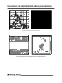
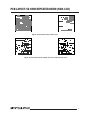
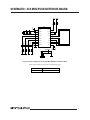
WIRELESS
DOCUMENTATION
IA ISM-UGRP
ISM Band Repeater Demo
User Guide
Version 2.0r - PRELIMINARY
IA ISM-UGRP Rev 2.0r 1205
© 2005, Integration Associates, Inc.
Integration Associates, Inc.
110 Pioneer Way, Unit L
Mountain View, California 94041
Tel: 650.969.4100
Fax: 650.969.4582
www.integration.com
[email protected]
[email protected]
ISM Band Repeater Demo
User Guide
Version 2.0r - Preliminary
Revision Date: December 15, 2005
The information is provided “as is” without any express or implied warranty of any kind,
including warranties of merchantability, non-infringement of intellectual property, or fitness
for any particular purpose. In no event shall Integration Associates, Inc., or its suppliers
be liable for any damages whatsoever arising out of the use of or an inability to use the
materials. Integration Associates, Inc., and its suppliers further do not warrant the accuracy
or completeness of the information, text, graphics, or other items contained within these
materials. Integration Associates, Inc., may make changes to these materials, or to the
products described within, at any time, without notice.
© 2005 Integration Associates, Inc. All rights reserved. Integration Associates is a trademark
of Integration Associates, Inc. All trademarks belong to their respective owners.
i
ABOUT THIS GUIDE
The ISM Band Repeater Demo is designed to show the use of Integration's IA4220/IA4221/IA4320/IA4420 chipsets in a
multi-transmitter/receiver environment.
For further information on the devices found in this user guide, please visit our Web site: http://www.integration.com
and download the following datasheets:
IA4220 Universal ISM Band Transmitter datasheet:
IA4220-DS
IA4221 Universal ISM Band Transmitter datasheet:
IA4221-DS
IA4320 Universal ISM Band Receiver datasheet:
IA4320-DS
IA4420 Universal ISM Band Transceiver datasheet:
IA4420-DS
ii
TABLE OF CONTENTS
Demo Kit Contents ................................................................................................................................................. 1
Overview ...................................................................................................................................................................2
Repeater Demo Description ...................................................................................................................................4
Demo Unit Table of Contents .................................................................................................................................. 5
Radio Hardware: IA4220/21 Transmitter Section ............................................................................................. 7
Schematic ..................................................................................................................................................... 8
434 MHz Layouts ......................................................................................................................................... 9
915 MHz Layouts ........................................................................................................................................ 10
Radio Hardware: IA4420 Transceiver Section ................................................................................................. 11
Schematic:
50 Ohm Repeater Demo (LCD Version) ................................................................................. 12
.
PCB Layout: 50 Ohm Repeater Demo (LCD Version) ............................................................................... 13
Schematic: 50 Ohm Repeater Demo (Non-LCD Version) ......................................................................... 14
PCB Layout: 50 Ohm Repeater Demo (Non-LCD Version) ....................................................................... 15
Radio Hardware: IA4320 Receiver Section ...................................................................................................... 17
434 MHz Receiver Schematic ................................................................................................................... 18
434 MHz Receiver Layouts ........................................................................................................................ 19
915 MHz Receiver Schematic ................................................................................................................... 20
915 MHz Receiver Layouts ........................................................................................................................ 21
iii
DEMO KIT CONTENTS
This document describes designs available on the development kit CDROM for the 434 and 915 MHz ISM Repeater Demo.
Also covered are the diagrams for both LCD and non-LCD variants. For further details, please refer to www.integration.com/
evaluation_kits.php or the IA ISM-DKxx CDROM.
IA ISM-UGRP contains the following items:
• Push Button Demo transmitter board
• Two Push Button Demo receiver boards
• Repeater Demo board
• User Guide
This document is designed to provide as the user guide to all variants of the Repeater Demo. Photographs may differ
depending on version. The photograph above is the 434 MHz LCD version.
1
OVERVIEW
The demo’s main objective is to show the IA4420’s capability to monitor multiple frequencies, receive data from an FSK
transmitter, and then re-transmit this data on an another arbitrary frequency to another receiver or transceiver. This
demonstration is designed to show the IA4420 acting as a repeater node.
The Repeater Demo has three main components: the IA4420, which is the system radio, a C8051F311 type 8051
microcontroller, which controls the application, and a 2 line 16 character LCD, which informs the user of the repeater status
(Note)
.
The current version of the Repeater Demo is equipped with a 50 Ohm SMA connector for the antenna.
Controller
IA4420
ISM Transceiver
FIFO
TX Latch
SPI Interface
SW Uart Interface
TX/ RX buffer
Packet
Receiver
Packet
Builder
Packet
Transmitter
Repeater function
LCD
IA4420 control
Software parts in C8051F311
Physical layer
Serial
SPI Interface
Scheduler
LCD Interface
Fig. 1 Repeater Block Diagram
Note: LCD only available on some models.
2
OVERVIEW
The demo uses the developer-friendly features of the IA4420 device. In receive mode the microcontroller reads the received
bytes from the IA4420’s FIFO, and transmits them through the TX latch. This approach dramatically reduces the load on the
micro, because the microcontroller doesn’t have to monitor every bit, only the bytes. This means the timing constraints in
an application can be reduced at least by a factor of eight for both the transmitting and the receiving sides. See the
PROCESSOR ACTIVITY lines on Figure 2, as demonstrated for both the ‘Traditional’ transceiver mode and the Integration
‘FIFO’ mode.
"Traditional"
mode
byte1
DATA CLK
PROCESSOR ACTIVITY
FIFO mode
RF PACKETS (8bit)
1
2
3
4
5
INTERRUPT REQs
PROCESSOR ACTIVITY
FIFO IT level
set to 8 bit
FIFO LEVEL STATUS
FIFO empty
Fig 2. Process Activity in FIFO Mode when Compared to a Traditional Mode of Operation
3
DESCRIPTION
The frequency configuration of this demo is as follows:
•
One of the Push Button Demo receivers is set to a different frequency than that of the Push Button transmitter.
The other receiver is paired with the frequency of the transmitter.
•
The Repeater demo receiving frequency is set to the frequency of the Push Button demo transmitter.
The Repeater demo transmitting frequency is set to the non-paired Push Button demo receiver’s frequency
.
LED4
IA4320
LED3
LED2
LED1
Push Button Demo receiver on F1
IA4420
uC
S3
LCD
S4
S1
S2
IA4220
LED4
IA4320
LED3
LED2
LED1
Push Button Demo transmitter on F1
Repeater Demo transmitter,
receives on F1, transmits on F2
Note: Diagram may differ depending on type.
Push Button Demo receiver on F2
Fig. 3 Repeater Demo Arrangement
After power on, the Repeater Demo continually looks for a valid packet on the receiving frequency. This happens when one
button has been pressed on the Push Button Demo transmitter. At this moment the LED will light up on the paired Push
Button receiver board. After the Repeater Demo (transceiver board) properly receives this packet, it will forward the packet
on its transmitting frequency. At that time, the LED will light up on the non-paired Push Button receiver board, if both of the
Push Button Transmitter and Push Button Receiver are in the range of the Repeater Demo. It should be noted that the
transceiver in this demo adds a small time delay between receiving and transmitting. This is done to prove the transmitter
is not talking directly to the receiver. Depending on the button pressed, a different time delay is implemented.
A packet is valid if it contains the preamble bytes (0xAA), the synchron pattern (0x2DD4), and the data, which corresponds
to the Push Button Demo data structure.
It can be shown that the paired Push Button demo is working alone, but if the Repeater demo is operating, then both the
Push Button Receivers will work, and the RF communication range is significantly bigger than without the Repeater Demo.
4
Demo Unit
TABLE OF CONTENTS
Radio Hardware
Stage 1 – IA4220 Transmitter
Stage 2 – IA4420 Transceiver
Stage 3 – IA4320 Receiver
5
This page is intentionally left blank
6
Radio Hardware
IA4220/21 TRANSMITTER SECTION
Contents
- Schematic
- 434 MHz Layouts
- 915 MHz Layouts
7
SCHEMATIC: PUSH BUTTON DEMO TX BOARD
3
WP\
SO
2
GND
10u
C1
VCC
8
B1
C3
GND
R5
3k3
R4
SO
470
R1
R3
VCC
GND
3k3
100p 100n
-
R2
10 k
C2
6k8
+
D1
HOLD\
SCK
SI
CS\
VCC
1
2
3
7
6
5
1
SCK
SI
CS
SW1
EEPROM
Array
4
VCC
IC2
IC1
1
2
3
4
5
6
7
SCK
VDD
SEL
IRQ
WS1
RFP
WS2
RFN
WS3
MOD
WS4
VSS
CLK/SDO
XTL
16
15
14
13
12
11
10
9
GND
1
2
FSK
3
4
SMDRET
S4
1
2
3
4
SMDRET
S3
1
2
3
4
SMDRET
S2
1
2
3
4
SMDRET
S1
8
SDI
XTL
10 MHz
LED
1
GND
Fig 4. IA4220 434 MHz Push Button Transmitter Schematic
Antenna configuration, along with the configuration/frequency setting commands denote operating frequency.
Examples of the physical board differences can be seen on the following pages. It can be noted from these layouts that
only the antenna is different.
8
PCB LAYOUT: 434 MHZ PUSH BUTTON TX BOARD
Fig 5. 434 MHz Push Button Transmitter Board PCB Layout
Fig 6. IA4220 434 MHz Push Button Transmitter Board PCB Assembly Layout
9
PCB LAYOUT: 915 MHZ PUSH BUTTON TX BOARD
Fig 7. 915 MHz Push Button Transmitter Board PCB Layout
Fig 8. IA4220 915 MHz Push Button Transmitter Board PCB Assembly Layout
10
Radio Hardware
IA4420 TRANSCEIVER SECTION
Contents
- 50 Ohm Transceiver LCD Board
- 50 Ohm Transceiver Non-LCD Board
11
1
2
3
POWER
SERIAL
GND
GND
2,2uF
C3
GND
3 TX
2 RX
1
FFS
FFIT
INT/VDI
ARSSI
SCK
MISO
MOSI
IRQ
R8
22
21
20
19
18
17
16
15
IC3
OUT 5
IA2112-3.3V
GND
VDD
/RST/C2CK
3 ON POK 4
2 GND
1 IN
P2.0
P2.1
P2.2
P2.3
P2.4
P2.5
P2.6
P2.7
P3.0/C2D
C8051F311
P1.0
P1.1
P1.2
P1.3
P1.4
P1.5
P1.6
P1.7
P0.0
P0.1
P0.2
P0.3
P0.4
P0.5
P0.6
P0.7
2,2uF
C4
3,3V
GND
3
4
5
6
14
13
12
11
10
9
8
7
GND
GND
2
C1
ON
DEBUG
3
2
1
GND
100nF
VCC
820
R5
SCL
SDA
GND
1k
R7
820
R6
D3
Yellow
1
2
3
4
5
6
VLCD
VSS
VDD
SDA
POR
SCL
LCD
BT21605
NRES
GND
It is not mounted.
820
R4
1
2
3
VCC
D2
Green
VCC
They are not mounted.
R2
R1
GND
BATTERY
TX
RX
100k
SW1
R9
2
1
28
27
26
25
24
23
VCC
3 2 1
4,7k
R10
SJ1
2
NRES 1
+
-
6
7
FFS
FFIT
8
5
SEL
IRQ
3
SCK
4
2
MOSI
MISO
1
XTL/REF
NRES
1uF
GND
10pF
C7
VCC
14
GND
4,7nF
C2
10
9
NRES
11
12
Q1
10MHz
GND
ARSSI
15
13
INT/VDI
16
GND
X1
GND
VCC
Fig 9 . IA4420 Transceiver Repeater Demo Schematic
C6
100pF
C5
Only rev. C or above!
IA4420
CLK
DCLK/CFIL/FFIT
VSS
RF2
RF1
VDD
ARSSI
NINT/VDI
FSK/DATA/NFFS
NIRQ
SDO
NSEL
SCK
SDI
IC2
VCC
SEL
3
1
6
5
4
4,7k
R11
GND
D1
Red
4,7k
L1
L3
C8
C9
IC1
R3
10k
SDA
SCL
SCHEMATIC: 50 OHM REPEATER DEMO
12
PCB LAYOUT: 50 OHM REPEATER DEMO (LCD VERSION)
Fig 10. 50 Ohm Repeater Demo PCB Layout
Fig 11. 50 Ohm Repeater Demo IA4420 Transceiver PCB Assembly Layout
13
VCC
R1
GND
R2
1
2
6V
BATTERY
J1
GND
GND
3 TX
2 RX
1
FFS
FFIT
INT/VDI
ARSSI
SCK
MISO
MOSI
IRQ
22
21
20
19
18
17
16
15
2,2uF
C3
TX
RX
P3.0/C2D
P1.0
P1.1
P1.2
P1.3
P1.4
P1.5
P1.6
P1.7
OUT 5
IA2112-3.3V
3 ON POK 4
2 GND
1 IN
IC3
C8051F311
GND
VDD
/RST/C2CK
P2.0
P2.1
P2.2
P2.3
P2.4
P2.5
P2.6
P2.7
GND
3
4
5
6
14
13
12
11
10
9
8
7
2,2uF
C4
3,3V
GND
1
4
3
6
DEBUG
3
2
1
GND
100nF
C1
VCC
D1
Red
1uF
C5
820
R5
820
R4
820
R3 GND
5
SW1
D2
Green
100pF
C6
1k
R7
820
R6
VCC
D3
Yellow
D4
Red
NRES
GND
10pF
C7
VCC
IC1
6
7
FFIT
SDI
Only rev. C or above!
IA4420
NRES
XTL/REF
DCLK/CFIL/FFIT
CLK
VSS
RF2
RF1
VDD
ARSSI
NINT/VDI
FSK/DATA/NFFS
NIRQ
SDO
NSEL
SCK
9
10
11
12
13
14
15
16
GND
4,7nF
C2
Q1
10MHz
GND
VCC
ARSSI
INT/VDI
GND
X1
GND
Fig 12. IA4420 Transceiver Repeater Demo Non-LCD Schematic
8
5
IRQ
FFS
4
3
SEL
MISO
1
2
MOSI
SCK
IC2
GND
SJ1
2
NRES 1
R8
P0.0
P0.1
P0.2
P0.3
P0.4
P0.5
P0.6
P0.7
100k
L1
L3
2
1
28
27
26
25
24
23
VCC
C8
C9
VCC
SEL
SCHEMATIC: 50 OHM REPEATER DEMO (NON-LCD)
14
PCB LAYOUT: 50 OHM REPEATER DEMO (NON-LCD)
Fig 13. 50 Ohm Repeater Demo PCB Layout
Fig 14 50 Ohm Repeater Demo IA4420 Transceiver PCB Assembly Layout
15
This page is intentionally left blank
16
Radio Hardware
IA4320 RECEIVER SECTION
Contents
- Schematic
- 434 MHz Layouts
- 915 MHz Layouts
17
SCHEMATIC: 434 MHZ PUSH BUTTON RX BOARD
0R
0R
R6
R5
GND GND
C3
C2
C1
2
10u
10n
10p
3
4
5
7
LED4
RED
LED3 RED
LED2 RED
LED1 RED
6
8
FCS0
FCS3
FBS0
FCS2
FBS1
VDD
OUT0
IN1
OUT1
IN2
OUT2
VSS
OUT3
FCS1
LPDM
XTL
VDD
VDD
13
12
11
10
-
GND
G1
SW1
1
2
3
GND GND GND GND
14
GND
B2430UNI
+
15
9
IA4320
470
470
R1
470
R2
470
R3
R4
GND
16
XTAL
1
10MHz
VDD
IC
GND
Fig 15. Example configuration for the 434 MHz IA4320 in Standalone Mode
Solder resistors R5, R6 according to the following table:
433.36 MHz
R5, R6 = 0 Ohm
434.32 MHz
R5, R6 not present
18
PCB LAYOUT: 434 MHZ PUSH BUTTON RX BOARD
Lit.3V
0x20,3
10,2x17,8
7,5x20,3
10,2x20,3
Fig 16. 434 MHz Push Button Receiver Board PCB Layout
Fig 17. IA4320 434 MHz Push Button Receiver Board PCB Assembly Layout
19
SCHEMATIC: 915 MHZ PUSH BUTTON RX BOARD
2
2
10uF 10n 10p
3
1
3
FCS0
4
GND
2
FCS1
1
FCS3
2
LPDM
3
1
LPDM
RED LED4
RED LED3
1
3
R4 470
2
FCS3
R3 470
1
FCS2
RED LED2
3
6
RED LED1
2
FCS2
R2 470
FCS1
R1 470
3
5
GND GND GND GND
7
LPDM
8
IC
FCS0
FBS0
FCS2
FBS1
VDD
OUT0
OUT1
OUT2
OUT3
LPDM
POWER
2
1
FCS3
IN1
IN2
VSS
FCS1
XTL
VDD
VDD=2.2V - 5.5V
GND
16
FCS3
15
FCS2
VDD
14
Antenna
C1
1
13
12
11
10
FCS1
9
10MHz
XTAL
FCS0
FCS0
IA4320
VDD
C3 C2
GND
GND
Fig 15. Example configuration for the 915 MHz IA4320 in Standalone Mode
908.64 MHz
LPDM=0, FCS0=0, FCS1=0, FCS2=NC, FCS3=0
916.32 MHz
LPDM=0, FCS0=0, FCS1=0, FCS2=0, FCS3=NC
20
PCB LAYOUT: 915 MHZ PUSH BUTTON RX BOARD
Fig 18. 915 MHz Push Button Receiver Board PCB Layout
Fig 19. 915 MHz Push Button Receiver Board PCB Assembly Layout
21
Integration Associates, Inc.
110 Pioneer Way, Unit L
Mountain View, California 94041
Tel: 650.969.4100
Fax: 650.969.4582
www.integration.com
[email protected]
[email protected]
P694
This document may contain preliminary information and is subject to change
by Integration Associates, Inc. without notice. Integration Associates
assumes no responsibility or liability for any use of the information
contained herein. Nothing in this document shall operate as an express or
implied license or indemnity under the intellectual property rights of
Integration Associates or third parties. The products described in this
document are not intended for use in implantation or other direct life
support applications where malfunction may result in the direct physical
harm or injury to persons. NO WARRANTIES OF ANY KIND, INCLUDING, BUT
NOT LIMITED TO, THE IMPLIED WARRANTIES OF MECHANTABILITY OR FITNESS
FOR A PARTICULAR PURPOSE, ARE OFFERED IN THIS DOCUMENT.
©2005, Integration Associates, Inc. All rights reserved. Integration Associates is a trademark of Integration
Associates, Inc. All other trademarks belong to their respective owners.
22