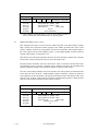
1
03)[[[$+
',6.'5,9(6
352'8&70$18$/
C141-E106-02EN
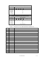
5(9,6,215(&25'
(GLWLRQ
'DWHSXEOLVKHG
)HE
-XQH
5HYLVHGFRQWHQWV
&RUUHFWLRQRIVSHFLILFDWLRQRQSRZHUGLVVLSDWLRQ7DEOH
6SHFLILFDWLRQ1R&((1
7KHFRQWHQWVRIWKLVPDQXDOLVVXEMHFWWRFKDQJH
ZLWKRXWSULRUQRWLFH
$OO5LJKWV5HVHUYHG
&RS\ULJKW¤)8-,768/,0,7('
&((1
L
7KLVSDJHLVLQWHQWLRQDOO\OHIWEODQN
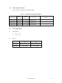
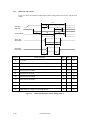
0$18$/25*$1,=$7,21
03)[[[$+
',6.'5,9(6
352'8&7
0$18$/
&(
7KLVPDQXDO!
03)[[[$+
',6.'5,9(6
0$,17(1$1&(
0$18$/
&)
'(9,&(29(59,(:
'(9,&(&21),*85$7,21
,167$//$7,21&21',7,216
7+(25<2)'(9,&(23(5$7,21
,17(5)$&(
23(5$7,216
0$,17(1$1&($1'',$*126,6
5(029$/$1'5(3/$&(0(17352&('85(
&((1
LLL
7KLVSDJHLVLQWHQWLRQDOO\OHIWEODQN
35()$&(
7KLVPDQXDOGHVFULEHVWKH03)[[[$+VHULHVDLQFKKDUGGLVNGULYHZLWKD%8,/7,1FRQWUROOHUWKDW
LVFRPSDWLEOHZLWKWKH$7$LQWHUIDFH
7KLVPDQXDOH[SODLQVLQGHWDLOKRZWRLQFRUSRUDWHWKHKDUGGLVNGULYHVLQWRXVHUV\VWHPV
7KLV PDQXDO DVVXPHV WKDW XVHUV KDYH D EDVLF NQRZOHGJH RI KDUG GLVN GULYHV DQG WKHLU DSSOLFDWLRQ LQ
FRPSXWHUV\VWHPV
7KLVPDQXDOFRQVLVWVRIWKHIROORZLQJVL[FKDSWHUV
&KDSWHU
'(9,&(29(59,(:
&KDSWHU
'(9,&(&21),*85$7,21
&KDSWHU
,167$//$7,21&21',7,216
&KDSWHU
7+(25<2)'(9,&(23(5$7,21
&KDSWHU
,17(5)$&(
&KDSWHU
23(5$7,216
,QWKLVPDQXDOGLVNGULYHVPD\EHUHIHUUHGWRDVGULYHVRUGHYLFHV
&((1
Y
&RQYHQWLRQVIRU$OHUW0HVVDJHV
7KLVPDQXDOXVHVWKHIROORZLQJFRQYHQWLRQVWRVKRZWKHDOHUWPHVVDJHV$QDOHUWPHVVDJHFRQVLVWVRIDQ
DOHUWVLJQDODQGDOHUWVWDWHPHQWV7KHDOHUWVLJQDOFRQVLVWVRIDQDOHUWV\PERODQGDVLJQDOZRUGRUMXVWD
VLJQDOZRUG
7KHIROORZLQJDUHWKHDOHUWVLJQDOVDQGWKHLUPHDQLQJV
7KLVLQGLFDWHVDKD]DUGRXVVLWXDWLRQOLNHO\WRUHVXOWLQVHULRXVSHUVRQDO
LQMXU\LIWKHXVHUGRHVQRWSHUIRUPWKHSURFHGXUHFRUUHFWO\
7KLVLQGLFDWHVDKD]DUGRXVVLWXDWLRQFRXOGUHVXOWLQSHUVRQDOLQMXU\LIWKH
XVHUGRHVQRWSHUIRUPWKHSURFHGXUHFRUUHFWO\
7KLVLQGLFDWHVDKD]DUGRXVVLWXDWLRQFRXOGUHVXOWLQPLQRURUPRGHUDWH
SHUVRQDOLQMXU\LIWKHXVHUGRHVQRWSHUIRUPWKHSURFHGXUHFRUUHFWO\7KLV
DOHUWVLJQDODOVRLQGLFDWHVWKDWGDPDJHVWRWKHSURGXFWRURWKHUSURSHUW\
PD\RFFXULIWKHXVHUGRHVQRWSHUIRUPWKHSURFHGXUHFRUUHFWO\
7KLVLQGLFDWHVLQIRUPDWLRQWKDWFRXOGKHOSWKHXVHUXVHWKHSURGXFWPRUH
HIILFLHQWO\
,Q WKH WH[W WKH DOHUW VLJQDO LV FHQWHUHG IROORZHG EHORZ E\ WKH LQGHQWHG PHVVDJH $ ZLGHU OLQH VSDFH
SUHFHGHVDQGIROORZVWKHDOHUWPHVVDJHWRVKRZZKHUHWKHDOHUWPHVVDJHEHJLQVDQGHQGV7KHIROORZLQJLV
DQH[DPSOH
([DPSOH
,03257$17
+$ KRVW DGDSWHU FRQVLVWV RI DGGUHVV GHFRGHU GULYHU DQG UHFHLYHU
$7$ LV DQ DEEUHYLDWLRQ RI $7 DWWDFKPHQW 7KH GLVN GULYH LV
FRQIRUPHGWRWKH$7$LQWHUIDFH
7KHPDLQDOHUWPHVVDJHVLQWKHWH[WDUHDOVROLVWHGLQWKH¦,PSRUWDQW$OHUW,WHPV§
YL
&((1
/,$%,/,7<(;&(37,21
'LVNGULYHGHIHFWVUHIHUVWRGHIHFWVWKDWLQYROYHDGMXVWPHQWUHSDLURUUHSODFHPHQW
)XMLWVX LV QRW OLDEOH IRU DQ\ RWKHU GLVN GULYH GHIHFWV VXFK DV WKRVH FDXVHG E\ XVHU PLVRSHUDWLRQ RU
PLVKDQGOLQJLQDSSURSULDWHRSHUDWLQJHQYLURQPHQWVGHIHFWVLQWKHSRZHUVXSSO\RUFDEOHSUREOHPVRIWKH
KRVWV\VWHPRURWKHUFDXVHVRXWVLGHWKHGLVNGULYH
&((1
YLL
7KLVSDJHLVLQWHQWLRQDOO\OHIWEODQN
&217(176
SDJH
&+$37(5
'(9,&(29(59,(: )HDWXUHV )XQFWLRQVDQGSHUIRUPDQFH $GDSWDELOLW\ ,QWHUIDFH 'HYLFH6SHFLILFDWLRQV 6SHFLILFDWLRQVVXPPDU\ 0RGHODQGSURGXFWQXPEHU 3RZHU5HTXLUHPHQWV (QYLURQPHQWDO6SHFLILFDWLRQV $FRXVWLF1RLVH 6KRFNDQG9LEUDWLRQ 5HOLDELOLW\ (UURU5DWH 0HGLD'HIHFWV &+$37(5
'(9,&(&21),*85$7,21 'HYLFH&RQILJXUDWLRQ 6\VWHP&RQILJXUDWLRQ $7$LQWHUIDFH GULYHFRQQHFWLRQ GULYHVFRQQHFWLRQ &+$37(5
,167$//$7,21&21',7,216 'LPHQVLRQV +DQGOLQJ&DXWLRQV *HQHUDOQRWHV ,QVWDOODWLRQ 5HFRPPHQGHGHTXLSPHQWV 0RXQWLQJ &DEOH&RQQHFWLRQV 'HYLFHFRQQHFWRU &((1
L[
&DEOHFRQQHFWRUVSHFLILFDWLRQV 'HYLFHFRQQHFWLRQ 3RZHUVXSSO\FRQQHFWRU&1 6\VWHPFRQILJXUDWLRQIRU8OWUD'0$ -XPSHU6HWWLQJV /RFDWLRQRIVHWWLQJMXPSHUV )DFWRU\GHIDXOWVHWWLQJ -XPSHUFRQILJXUDWLRQ &+$37(5
7+(25<2)'(9,&(23(5$7,21 2XWOLQH 6XEDVVHPEOLHV 'LVN +HDG 6SLQGOH $FWXDWRU $LUILOWHU &LUFXLW&RQILJXUDWLRQ 3RZHURQ6HTXHQFH 6HOIFDOLEUDWLRQ 6HOIFDOLEUDWLRQFRQWHQWV ([HFXWLRQWLPLQJRIVHOIFDOLEUDWLRQ &RPPDQGSURFHVVLQJGXULQJVHOIFDOLEUDWLRQ 5HDGZULWH&LUFXLW 5HDGZULWHSUHDPSOLILHU3UH$03 :ULWHFLUFXLW 5HDGFLUFXLW 6\QWKHVL]HUFLUFXLW 6HUYR&RQWURO 6HUYRFRQWUROFLUFXLW 'DWDVXUIDFHVHUYRIRUPDW 6HUYRIUDPHIRUPDW $FWXDWRUPRWRUFRQWURO 6SLQGOHPRWRUFRQWURO [
&((1
&+$37(5
,17(5)$&( 3K\VLFDO,QWHUIDFH ,QWHUIDFHVLJQDOV 6LJQDODVVLJQPHQWRQWKHFRQQHFWRU /RJLFDO,QWHUIDFH ,2UHJLVWHUV &RPPDQGEORFNUHJLVWHUV &RQWUROEORFNUHJLVWHUV +RVW&RPPDQGV &RPPDQGFRGHDQGSDUDPHWHUV &RPPDQGGHVFULSWLRQV (UURUSRVWLQJ &RPPDQG3URWRFRO 'DWDWUDQVIHUULQJFRPPDQGVIURPGHYLFHWRKRVW 'DWDWUDQVIHUULQJFRPPDQGVIURPKRVWWRGHYLFH &RPPDQGVZLWKRXWGDWDWUDQVIHU 2WKHUFRPPDQGV '0$GDWDWUDQVIHUFRPPDQGV 8OWUD'0$IHDWXUHVHW 2YHUYLHZ 3KDVHVRIRSHUDWLRQ 8OWUD'0$GDWDLQFRPPDQGV ,QLWLDWLQJDQ8OWUD'0$GDWDLQEXUVW 7KHGDWDLQWUDQVIHU 3DXVLQJDQ8OWUD'0$GDWDLQEXUVW 7HUPLQDWLQJDQ8OWUD'0$GDWDLQEXUVW 8OWUD'0$GDWDRXWFRPPDQGV ,QLWLDWLQJDQ8OWUD'0$GDWDRXWEXUVW 7KHGDWDRXWWUDQVIHU 3DXVLQJDQ8OWUD'0$GDWDRXWEXUVW 7HUPLQDWLQJDQ8OWUD'0$GDWDRXWEXUVW 8OWUD'0$&5&UXOHV 6HULHVWHUPLQDWLRQUHTXLUHGIRU8OWUD'0$ 7LPLQJ 3,2GDWDWUDQVIHU 0XOWLZRUGGDWDWUDQVIHU &((1
[L
8OWUD'0$GDWDWUDQVIHU ,QLWLDWLQJDQ8OWUD'0$GDWDLQEXUVW 8OWUD'0$GDWDEXUVWWLPLQJUHTXLUHPHQWV 6XVWDLQHG8OWUD'0$GDWDLQEXUVW +RVWSDXVLQJDQ8OWUD'0$GDWDLQEXUVW 'HYLFHWHUPLQDWLQJDQ8OWUD'0$GDWDLQEXUVW +RVWWHUPLQDWLQJDQ8OWUD'0$GDWDLQEXUVW ,QLWLDWLQJDQ8OWUD'0$GDWDRXWEXUVW 6XVWDLQHG8OWUD'0$GDWDRXWEXUVW 'HYLFHSDXVLQJDQ8OWUD'0$GDWDRXWEXUVW +RVWWHUPLQDWLQJDQ8OWUD'0$GDWDRXWEXUVW 'HYLFHWHUPLQDWLQJDQ8OWUD'0$GDWDLQEXUVW 3RZHURQDQGUHVHW &+$37(5
23(5$7,216 'HYLFH5HVSRQVHWRWKH5HVHW 5HVSRQVHWRSRZHURQ 5HVSRQVHWRKDUGZDUHUHVHW 5HVSRQVHWRVRIWZDUHUHVHW 5HVSRQVHWRGLDJQRVWLFFRPPDQG $GGUHVV7UDQVODWLRQ 'HIDXOWSDUDPHWHUV /RJLFDODGGUHVV 3RZHU6DYH 3RZHUVDYHPRGH 3RZHUFRPPDQGV 'HIHFW0DQDJHPHQW 6SDUHDUHD $OWHUQDWLQJGHIHFWLYHVHFWRUV 5HDG$KHDG&DFKH 'DWDEXIIHUFRQILJXUDWLRQ &DFKLQJRSHUDWLRQ 8VDJHRIUHDGVHJPHQW :ULWH&DFKH [LL
&((1
),*85(6
SDJH
&XUUHQWIOXFWXDWLRQ7\SZKHQSRZHULVWXUQHGRQ 'LVNGULYHRXWHUYLHZ GULYHV\VWHPFRQILJXUDWLRQ GULYHVFRQILJXUDWLRQ 'LPHQVLRQV +DQGOLQJFDXWLRQV 'LUHFWLRQ /LPLWDWLRQRIVLGHPRXQWLQJ 0RXQWLQJIUDPHVWUXFWXUH 6XUIDFHWHPSHUDWXUHPHDVXUHPHQWSRLQWV 6HUYLFHDUHD &RQQHFWRUORFDWLRQV &DEOHFRQQHFWLRQV 3RZHUVXSSO\FRQQHFWRUSLQV&1 &DEOHFRQILJXUDWLRQ &DEOHW\SHGHWHFWLRQXVLQJ&%/,'VLJQDO
+RVWVHQVLQJWKHFRQGLWLRQRIWKH&%/,'VLJQDO &DEOHW\SHGHWHFWLRQXVLQJ,'(17,)<'(9,&(GDWD
'HYLFHVHQVLQJWKHFRQGLWLRQRIWKH&%/,'VLJQDO -XPSHUORFDWLRQ )DFWRU\GHIDXOWVHWWLQJ -XPSHUVHWWLQJRIPDVWHURUVODYHGHYLFH -XPSHUVHWWLQJRI&DEOH6HOHFW ([DPSOHRI&DEOH6HOHFW ([DPSOHRI&DEOH6HOHFW +HDGVWUXFWXUH 03)[[[$+%ORFNGLDJUDP 3RZHURQRSHUDWLRQVHTXHQFH %ORFNGLDJUDPRIVHUYRFRQWUROFLUFXLW 3K\VLFDOVHFWRUVHUYRFRQILJXUDWLRQRQGLVNVXUIDFH VHUYRIUDPHVLQHDFKWUDFN ([HFXWLRQH[DPSOHRI5($'08/7,3/(FRPPDQG 5HDG6HFWRUVFRPPDQGSURWRFRO &((1
[LLL
3URWRFROIRUFRPPDQGDERUW :5,7(6(&7256FRPPDQGSURWRFRO 3URWRFROIRUWKHFRPPDQGH[HFXWLRQZLWKRXWGDWDWUDQVIHU 1RUPDO'0$GDWDWUDQVIHU 8OWUD'0$WHUPLQDWLRQZLWKSXOOXSRUSXOOGRZQ 3,2GDWDWUDQVIHUWLPLQJ 0XOWLZRUG'0$GDWDWUDQVIHUWLPLQJPRGH ,QLWLDWLQJDQ8OWUD'0$GDWDLQEXUVW 6XVWDLQHG8OWUD'0$GDWDLQEXUVW +RVWSDXVLQJDQ8OWUD'0$GDWDLQEXUVW 'HYLFHWHUPLQDWLQJDQ8OWUD'0$GDWDLQEXUVW +RVWWHUPLQDWLQJDQ8OWUD'0$GDWDLQEXUVW ,QLWLDWLQJDQ8OWUD'0$GDWDRXWEXUVW 6XVWDLQHG8OWUD'0$GDWDRXWEXUVW 'HYLFHSDXVLQJDQ8OWUD'0$GDWDRXWEXUVW +RVWWHUPLQDWLQJDQ8OWUD'0$GDWDRXWEXUVW 'HYLFHWHUPLQDWLQJDQ8OWUD'0$GDWDRXWEXUVW 3RZHURQ5HVHW7LPLQJ 5HVSRQVHWRSRZHURQ 5HVSRQVHWRKDUGZDUHUHVHW 5HVSRQVHWRVRIWZDUHUHVHW 5HVSRQVHWRGLDJQRVWLFFRPPDQG $GGUHVVWUDQVODWLRQH[DPSOHLQ&+6PRGH $GGUHVVWUDQVODWLRQH[DPSOHLQ/%$PRGH 6HFWRUVOLSSURFHVVLQJ $OWHUQDWHF\OLQGHUDVVLJQPHQW 'DWDEXIIHUFRQILJXUDWLRQ [LY
&((1
7$%/(6
SDJH
6SHFLILFDWLRQV 0RGHOQDPHVDQGSURGXFWQXPEHUV &XUUHQWDQGSRZHUGLVVLSDWLRQ (QYLURQPHQWDOVSHFLILFDWLRQV $FRXVWLFQRLVHVSHFLILFDWLRQ 6KRFNDQGYLEUDWLRQVSHFLILFDWLRQ 6XUIDFHWHPSHUDWXUHPHDVXUHPHQWSRLQWVDQGVWDQGDUGYDOXHV &DEOHFRQQHFWRUVSHFLILFDWLRQV 6HOIFDOLEUDWLRQH[HFXWLRQWLPHFKDUW 7UDQVIHUUDWHRIHDFK]RQH ,QWHUIDFHVLJQDOV 6LJQDODVVLJQPHQWRQWKHLQWHUIDFHFRQQHFWRU ,2UHJLVWHUV &RPPDQGFRGHDQGSDUDPHWHUV ,QIRUPDWLRQWREHUHDGE\,'(17,)<'(9,&(FRPPDQG )HDWXUHVUHJLVWHUYDOXHVDQGVHWWDEOHPRGHV 'LDJQRVWLFFRGH )HDWXUHV5HJLVWHUYDOXHVVXEFRPPDQGVDQGIXQFWLRQV )RUPDWRIGHYLFHDWWULEXWHYDOXHGDWD )RUPDWRILQVXUDQFHIDLOXUHWKUHVKROGYDOXHGDWD &RQWHQWVRIVHFXULW\SDVVZRUG &RQWHQWVRI6(&85,7<6(73$66:25'GDWD 5HODWLRQVKLSEHWZHHQFRPELQDWLRQRI,GHQWLILHUDQG6HFXULW\OHYHO
DQGRSHUDWLRQRIWKHORFNIXQFWLRQ &RPPDQGFRGHDQGSDUDPHWHUV 5HFRPPHQGHGVHULHVWHUPLQDWLRQIRU8OWUD'0$ 8OWUD'0$GDWDEXUVWWLPLQJUHTXLUHPHQWV 'HIDXOWSDUDPHWHUV &((1
[Y
7KLVSDJHLVLQWHQWLRQDOO\OHIWEODQN
&+$37(5
'(9,&(29(59,(:
)HDWXUHV
'HYLFH6SHFLILFDWLRQV
3RZHU5HTXLUHPHQWV
(QYLURQPHQWDO6SHFLILFDWLRQV
$FRXVWLF1RLVH
6KRFNDQG9LEUDWLRQ
5HOLDELOLW\
(UURU5DWH
0HGLD'HIHFWV
2YHUYLHZ DQG IHDWXUHV DUH GHVFULEHG LQ WKLV FKDSWHU DQG VSHFLILFDWLRQV DQG SRZHU UHTXLUHPHQW DUH
GHVFULEHG
7KH03)[[[$+ VHULHV DUH D LQFK KDUG GLVN GULYH ZLWK D EXLOWLQ $7$ FRQWUROOHU 7KH GLVN GULYH LV
FRPSDFWDQGUHOLDEOH
)HDWXUHV
)XQFWLRQVDQGSHUIRUPDQFH
&RPSDFW
7KHGLVNKDVRUGLVNVRIPPLQFKHVGLDPHWHUDQGLWVKHLJKWLVPPLQFK
/DUJHFDSDFLW\
7KH GLVN GULYH FDQ UHFRUG XS WR *% IRUPDWWHG RQ RQH GLVN XVLQJ WKH ((350/
UHFRUGLQJPHWKRGDQGUHFRUGLQJ]RQHWHFKQRORJ\7KH03)[[[$+VHULHVKDYHDIRUPDWWHG
FDSDFLW\RI*%WR*%UHVSHFWLYHO\
+LJKVSHHG7UDQVIHUUDWH
7KHGLVNGULYHKDVDQLQWHUQDOGDWDUDWHXSWR0%V7KHGLVNGULYHVXSSRUWVDQH[WHUQDOGDWD
UDWHXSWR0%VRU0%VXOWUD'0$PRGH
&((1
$YHUDJHSRVLWLRQLQJWLPH
8VH RI D URWDU\ YRLFH FRLO PRWRU LQ WKH KHDG SRVLWLRQLQJ PHFKDQLVP JUHDWO\ LQFUHDVHV WKH
SRVLWLRQLQJVSHHG7KHDYHUDJHSRVLWLRQLQJWLPHLVPVDWUHDG
$GDSWDELOLW\
3RZHUVDYHPRGH
7KHSRZHUVDYHPRGHIHDWXUHIRULGOHRSHUDWLRQVWDQGE\DQGVOHHSPRGHVPDNHVWKHGLVNGULYH
LGHDOIRUDSSOLFDWLRQVZKHUHSRZHUFRQVXPSWLRQLVDIDFWRU
:LGHWHPSHUDWXUHUDQJH
7KHGLVNGULYHFDQEHXVHGRYHUDZLGHWHPSHUDWXUHUDQJH&WR&
/RZQRLVHDQGYLEUDWLRQ
,Q5HDG\VWDWXVWKHQRLVHRIWKHGLVNGULYHLVRQO\DERXWEHOV03)$+7\SLFDO6RXQG
3RZHUSHU,62DQG,62
,QWHUIDFH
&RQQHFWLRQWRLQWHUIDFH
:LWKWKHEXLOWLQ$7$LQWHUIDFHFRQWUROOHUWKHGLVNGULYHFDQEHFRQQHFWHGWRDQ$7$LQWHUIDFHRI
DSHUVRQDOFRPSXWHU
0%GDWDEXIIHU
7KHGLVNGULYHXVHVD0%GDWDEXIIHUWRWUDQVIHUGDWDEHWZHHQWKHKRVWDQGWKHGLVNPHGLD
,Q FRPELQDWLRQ ZLWK WKH UHDGDKHDG FDFKH V\VWHP GHVFULEHG LQ LWHP DQG WKH ZULWH FDFKH
GHVFULEHGLQLWHPWKHEXIIHUFRQWULEXWHVWRHIILFLHQW,2SURFHVVLQJ
5HDGDKHDGFDFKHV\VWHP
$IWHU WKH H[HFXWLRQ RI D GLVN UHDG FRPPDQG WKH GLVN GULYH DXWRPDWLFDOO\ UHDGV WKH VXEVHTXHQW
GDWDEORFNDQGZULWHVLWWRWKHGDWDEXIIHUUHDGDKHDGRSHUDWLRQ7KLVFDFKHV\VWHPHQDEOHVIDVW
GDWDDFFHVV7KHQH[WGLVNUHDGFRPPDQGZRXOGQRUPDOO\FDXVHDQRWKHUGLVNDFFHVV%XWLIWKH
UHDG DKHDG GDWD FRUUHVSRQGV WR WKH GDWD UHTXHVWHG E\ WKH QH[W UHDG FRPPDQG WKH GDWD LQ WKH
EXIIHUFDQEHWUDQVIHUUHGLQVWHDG
0DVWHUVODYH
7KH GLVN GULYH FDQ EH FRQQHFWHG WR $7$ LQWHUIDFH DV GDLV\ FKDLQ FRQILJXUDWLRQ 'ULYH LV D
PDVWHUGHYLFHGULYHLVDVODYHGHYLFH
&((1
(UURUFRUUHFWLRQDQGUHWU\E\(&&
,IDUHFRYHUDEOHHUURURFFXUVWKHGLVNGULYHLWVHOIDWWHPSWVHUURUUHFRYHU\7KHE\WHV(&&KDV
LPSURYHGEXIIHUHUURUFRUUHFWLRQIRUFRUUHFWDEOHGDWDHUURUV
:ULWHFDFKH
:KHQWKHGLVNGULYHUHFHLYHVDZULWHFRPPDQGWKHGLVNGULYHSRVWVWKHFRPPDQGFRPSOHWLRQDW
FRPSOHWLRQRIWUDQVIHUULQJGDWDWRWKHGDWDEXIIHUFRPSOHWLRQRIZULWLQJWRWKHGLVNPHGLD7KLV
IHDWXUHUHGXFHVWKHDFFHVVWLPHDWZULWLQJ
&((1
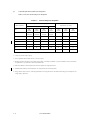
'HYLFH6SHFLILFDWLRQV
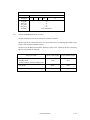
6SHFLILFDWLRQVVXPPDU\
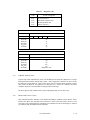
7DEOHVKRZVWKHVSHFLILFDWLRQVRIWKHGLVNGULYH
7DEOH
6SHFLILFDWLRQV
03)$+
03)$+
03)$+
*%
*%
*%
1XPEHURI'LVNV
1XPEHURI+HDGV
)RUPDWWHG&DSDFLW\
1XPEHURI&\OLQGHUV
8VHU$OWHUQDWH6$
%\WHVSHU6HFWRU
5HFRUGLQJ0HWKRG
((350/
7UDFN'HQVLW\
73,
%LW'HQVLW\
%3,
5RWDWLRQDO6SHHG
USP
$YHUDJH/DWHQF\
PV
3RVLWLRQLQJWLPH
0LQLPXP
$YHUDJH
0D[LPXP
PVW\SLFDO
5HDGPVW\SLFDO:ULWHPVW\SLFDO
5HDGPVW\SLFDO:ULWHPVW\SLFDO
6WDUW6WRSWLPH
6WDUWUSPWR'ULYH5HDG
6WRSDW3RZHU'RZQ
7\SLFDOVHF
7\SLFDOVHF
,QWHUIDFH
0D[LPXPVHF
0D[LPXPVHF
$7$¤
0D[LPXP&DEOHOHQJWKP
'DWD7UDQVIHU5DWH
7R)URP0HGLD
7R)URP+RVW
WR0%V
0%V0D[EXUVW3,2PRGHEXUVW'0$PRGH0%V0D[EXUVWXOWUD'0$PRGH
'DWDEXIIHU
0%
3K\VLFDO'LPHQVLRQV
+HLJKWu:LGWKu'HSWK
PPPD[ÕPPÕPP
§PD[Õ§Õ§
:HLJKW
J
&DSDFLW\XQGHUWKH/%$PRGH
8QGHUWKH&+6PRGHQRUPDO%,26VSHFLILFDWLRQIRUPDWWHGFDSDFLW\QXPEHURIF\OLQGHUVQXPEHURIKHDGVDQGQXPEHURI
VHFWRUVDUHDVIROORZV
0RGHO
)RUPDWWHG&DSDFLW\
1RRI&\OLQGHU
1RRI+HDGV
1RRI6HFWRUV
03)$+
0%
03)$+
0%
03)$+
0%
&((1
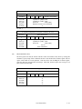
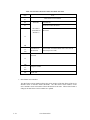
0RGHODQGSURGXFWQXPEHU
7DEOHOLVWVWKHPRGHOQDPHVDQGSURGXFWQXPEHUV
7DEOH
0RGHOQDPHVDQGSURGXFWQXPEHUV
0RGHO1DPH
&DSDFLW\
XVHUDUHD
0RXQWLQJ
6FUHZ
03)$+
*%
1R81&
&$%
¥
03)$+
*%
1R81&
&$%
¥
03)$+
*%
1R81&
&$%
¥
3RZHU5HTXLUHPHQWV
,QSXW9ROWDJH
x
x
2UGHU1R
5HPDUNV
9
9
5LSSOH
9
9
0D[LPXP
P9SHDNWRSHDN
P9SHDNWRSHDN
)UHTXHQF\
'&WR0+]
'&WR0+]
&((1
&XUUHQW5HTXLUHPHQWVDQG3RZHU'LVVLSDWLRQ
7DEOHOLVWVWKHFXUUHQWDQGSRZHUGLVVLSDWLRQ
7DEOH
&XUUHQWDQGSRZHUGLVVLSDWLRQ
7\SLFDO506FXUUHQW>P$@
0RGHRI2SHUDWLRQ
9
7\SLFDO3RZHU>ZDWWV@
9
0RGHO
03)
$+
03)
$+
03)
$+
$OO
0RGHOV
03)
$+
03)
$+
03)
$+
6SLQXS
WR
SHDN
WR
SHDN
WR
SHDN
WR
SHDN
,GOH5HDG\
5:2Q7UDFN
6HHN:5
6WDQGE\
6OHHS
$
%
%
(QHUJ\HIILFLHQF\UDQN>ZDWW*%@
&XUUHQWLVW\SLFDOUPVH[FHSWIRUVSLQXS
3RZHUUHTXLUHPHQWVUHIOHFWQRPLQDOYDOXHVIRU9DQG9SRZHU
,GOHPRGHLVLQHIIHFWZKHQWKHGULYHLVQRWUHDGLQJZULWLQJVHHNLQJRUH[HFXWLQJDQ\FRPPDQGV$SRUWLRQRIWKH5:FLUF XLWU\LVSRZHUHGGRZQ
WKHVSLQGOHPRWRULVXSWRVSHHGDQGWKH'ULYHUHDG\FRQGLWLRQH[LVWV
5:PRGHLVGHILQHGDVUHDGRSHUDWLRQVDQGZULWHRSHUDWLRQVRQDVLQJOHSK\VLFDOWUDFN
6HHN:5PRGHLVGHILQHGDVVHHNRSHUDWLRQVZULWHRSHUDWLRQVDQGUHDGRSHUDWLRQV
(QHUJ\HIILFLHQF\EDVHGRQWKH/DZFRQFHUQLQJWKH5DWLRQDO8VHRI(QHUJ\LQGLFDWHVWKHYDOXHREWDLQHGE\GLYLGLQJSRZHUFRQVXPSWLRQE\WKH
VWRUDJHFDSDFLW\-DSDQRQO\
&((1
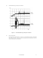
&XUUHQWIOXFWXDWLRQ7\SZKHQSRZHULVWXUQHGRQ
)LJXUH
&XUUHQWIOXFWXDWLRQ7\SZKHQSRZHULVWXUQHGRQ
3RZHURQRIIVHTXHQFH
7KHYROWDJHGHWHFWRUFLUFXLWPRQLWRUV9DQG97KHFLUFXLWGRHVQRWDOORZDZULWHVLJQDOLI
HLWKHUYROWDJHLVDEQRUPDO7KLVSUHYHQWVGDWDIURPEHLQJGHVWUR\HGDQGHOLPLQDWHVWKHQHHGWREH
FRQFHUQHGZLWKWKHSRZHURQRIIVHTXHQFH
&((1
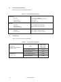
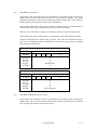
(QYLURQPHQWDO6SHFLILFDWLRQV
7DEOHOLVWVWKHHQYLURQPHQWDOVSHFLILFDWLRQV
7DEOH
7HPSHUDWXUH
2SHUDWLQJ
(QYLURQPHQWDOVSHFLILFDWLRQV
&WR&DPELHQW
&WR&GLVNHQFORVXUHVXUIDFH
¤&WR&
&KRXURUOHVV
1RQRSHUDWLQJ
7KHUPDO*UDGLHQW
+XPLGLW\
2SHUDWLQJ
1RQRSHUDWLQJ
0D[LPXP:HW%XOE
WR5+1RQFRQGHQVLQJ
WR5+1RQFRQGHQVLQJ
&
$OWLWXGHUHODWLYHWRVHDOHYHO
2SHUDWLQJ
1RQRSHUDWLQJ
¤WRP¤WRIW
¤WRP¤WRIW
$FRXVWLF1RLVH
7DEOHOLVWVWKHDFRXVWLFQRLVHVSHFLILFDWLRQ
7DEOH
6RXQG3RZHU
SHU,62DQG,62
7\SLFDODWP
6RXQG3UHVVXUH
7\SLFDODWP
$FRXVWLFQRLVHVSHFLILFDWLRQ
0RGHO
03)$+
03)$+
03)$+
,GOHPRGH'5,9(5($'<
EHOV
6HHNPRGH5DQGRP
EHOV
,GOHPRGH'5,9(5($'<
G%$
6HHNPRGH5DQGRP
G%$
&((1
6KRFNDQG9LEUDWLRQ
7DEOHOLVWVWKHVKRFNDQGYLEUDWLRQVSHFLILFDWLRQ
7DEOH
6KRFNDQGYLEUDWLRQVSHFLILFDWLRQ
9LEUDWLRQVZHSWVLQHRQHRFWDYHSHUPLQXWH
2SHUDWLQJ
1RQRSHUDWLQJ
WR+]*SHDN
ZLWKRXWQRQUHFRYHUHGHUURUV
WR+]*SHDNQRGDPDJH
6KRFNKDOIVLQHSXOVH2SHUDWLQJ
PVGXUDWLRQ
PVGXUDWLRQ
*ZLWKRXWQRQUHFRYHUHGHUURU
*ZLWKRXWQRQUHFRYHUHGHUURU
6KRFNKDOIVLQHSXOVH1RQRSHUDWLQJ
PVGXUDWLRQ
PVGXUDWLRQ
*7\SLFDOQRGDPDJH
*1RGDPDJH
5HOLDELOLW\
0HDQWLPHEHWZHHQIDLOXUHV07%)
7KHPHDQWLPHEHWZHHQIDLOXUHV07%)LV32+SRZHURQKRXUVRUPRUHRSHUDWLRQ
KRXUVGD\GD\VZHHN
7KLVGRHVQRWLQFOXGHIDLOXUHVRFFXUULQJGXULQJWKHILUVWWKUHHPRQWKVDIWHULQVWDOODWLRQ
07%)LVGHILQHGDVIROORZV
07%)
7RWDORSHUDWLRQWLPHLQDOOILHOGV
QXPEHURIGHYLFHIDLOXUHLQDOOILHOGV
+
'LVNGULYHGHIHFWVUHIHUVWRGHIHFWVWKDWLQYROYHUHSDLUUHDGMXVWPHQWRUUHSODFHPHQW'LVNGULYH
GHIHFWV GR QRW LQFOXGH IDLOXUHV FDXVHG E\ H[WHUQDO IDFWRUV VXFK DV GDPDJH FDXVHG E\ KDQGOLQJ
LQDSSURSULDWHRSHUDWLQJHQYLURQPHQWVGHIHFWVLQWKHSRZHUVXSSO\KRVWV\VWHPRULQWHUIDFHFDEOH
0HDQWLPHWRUHSDLU0775
7KH PHDQ WLPH WR UHSDLU 0775 LV PLQXWHV RU OHVV LI UHSDLUHG E\ D VSHFLDOLVW PDLQWHQDQFH
VWDIIPHPEHU
&66F\FOH
7KHQXPEHURI&66PXVWEHOHVVWKDQ
&((1
6HUYLFHOLIH
,QVLWXDWLRQVZKHUHPDQDJHPHQWDQGKDQGOLQJDUHFRUUHFWWKHGLVNGULYHUHTXLUHVQRRYHUKDXOIRU
ILYH\HDUVZKHQWKH'(VXUIDFHWHPSHUDWXUHLVOHVVWKDQ&:KHQWKH'(VXUIDFHWHPSHUDWXUH
H[FHHGV & WKH GLVN GULYHV UHTXLUHV QR RYHUKDXO IRU ILYH \HDUV RU KRXUV RI RSHUDWLRQ
ZKLFKHYHURFFXUVILUVW5HIHUWRLWHPLQ6XEVHFWLRQIRUWKHPHDVXUHPHQWSRLQWRIWKH'(
VXUIDFHWHPSHUDWXUH
'DWDDVVXUDQFHLQWKHHYHQWRISRZHUIDLOXUH
([FHSWIRUWKHGDWDEORFNEHLQJZULWWHQWRWKHGDWDRQWKHGLVNPHGLDLVDVVXUHGLQWKHHYHQWRIDQ\
SRZHUVXSSO\DEQRUPDOLWLHV7KLVGRHVQRWLQFOXGHSRZHUVXSSO\DEQRUPDOLWLHVGXULQJGLVNPHGLD
LQLWLDOL]DWLRQIRUPDWWLQJRUSURFHVVLQJRIGHIHFWVDOWHUQDWLYHEORFNDVVLJQPHQW
(UURU5DWH
.QRZQ GHIHFWV IRU ZKLFK DOWHUQDWLYH EORFNV FDQ EH DVVLJQHG DUH QRW LQFOXGHG LQ WKH HUURU UDWH
FRXQWEHORZ,WLVDVVXPHGWKDWWKHGDWDEORFNVWREHDFFHVVHGDUHHYHQO\GLVWULEXWHGRQWKHGLVN
PHGLD
8QUHFRYHUDEOHUHDGHUURU
5HDGHUURUVWKDWFDQQRWEHUHFRYHUHGE\UHDGUHWULHVZLWKRXWXVHU
VUHWU\DQG(&&FRUUHFWLRQVVKDOO
RFFXUQRPRUHWKDQWLPHVZKHQUHDGLQJGDWDRIELWV5HDGUHWULHVDUHH[HFXWHGDFFRUGLQJWR
WKH GLVN GULYH
V HUURU UHFRYHU\ SURFHGXUH DQG LQFOXGH UHDG UHWULHV DFFRPSDQ\LQJ KHDG RIIVHW
RSHUDWLRQV
3RVLWLRQLQJHUURU
3RVLWLRQLQJVHHNHUURUVWKDWFDQEHUHFRYHUHGE\RQHUHWU\VKDOORFFXUQRPRUHWKDQWLPHVLQ
VHHNRSHUDWLRQV
0HGLD'HIHFWV
'HIHFWLYHVHFWRUVDUHUHSODFHGZLWKDOWHUQDWHVZKHQWKHGLVNLVIRUPDWWHGSULRUWRVKLSPHQWIURP
WKHIDFWRU\ORZOHYHOIRUPDW7KXVWKHKRVWVHHVDGHIHFWIUHHGHYLFH
$OWHUQDWHVHFWRUVDUHDXWRPDWLFDOO\DFFHVVHGE\WKHGLVNGULYH7KHXVHUQHHGQRWEH FRQFHUQHG
ZLWKDFFHVVWRDOWHUQDWHVHFWRUV
&KDSWHUGHVFULEHVWKHORZOHYHOIRUPDWDWVKLSSLQJ
&((1
CHAPTER 2
2.1
DEVICE CONFIGURATION
2.1
Device Configuration
2.2
System Configuration
Device Configuration
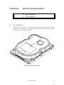
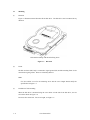
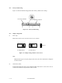
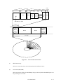
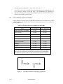
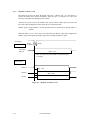
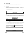
Figure 2.1 shows the disk drive. The disk drive consists of a disk enclosure (DE), read/write
preamplifier, and controller PCA. The disk enclosure contains the disk media, heads, spindle
motors actuators, and a circulating air filter.
Figure 2.1
Disk drive outerview
C141-E106-01EN
2-1
(1)
Disk
The outer diameter of the disk is 95 mm. The inner diameter is 25 mm. The number of disks
used varies with the model, as described below. The disks are rated at over 40,000 start/stop
operations.
MPF3102AH: 1 disks
MPF3153AH: 2 disks
MPF3204AH: 2 disks
(2)
Head
The heads are of the contact start/stop (CSS) type. The head touches the disk surface while the
disk is not rotating and automatically lifts when the disk starts.
(3)
Spindle motor
The disks are rotated by a direct drive Hall-less DC motor.
(4)
Actuator
The actuator uses a revolving voice coil motor (VCM) structure which consumes low power and
generates very little heat. The head assembly at the tip of the actuator arm is controlled and
positioned by feedback of the servo information read by the read/write head. If the power is not
on or if the spindle motor is stopped, the head assembly stays in the specific CSS zone on the
disk and is fixed by a mechanical lock.
(5)
Air circulation system
The disk enclosure (DE) is sealed to prevent dust and dirt from entering. The disk enclosure
features a closed loop air circulation system that relies on the blower effect of the rotating disk.
This system continuously circulates the air through the recirculation filter to maintain the
cleanliness of the air in the disk enclosure.
(6)
Read/write circuit
The read/write circuit uses a LSI chip for the read/write preamplifier. It improves data reliability
by preventing errors caused by external noise.
(7)
Controller circuit
The controller circuit consists of an LSI chip to improve reliability.
microprocessor unit (MPU) achieves a high-performance AT controller.
2-2
C141-E106-01EN
The high-speed
2.2
System Configuration
2.2.1
ATA interface
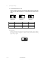
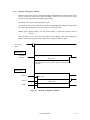
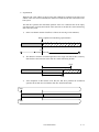
Figures 2.2 and 2.3 show the ATA interface system configuration. The drive has a 40-pin PC
AT interface connector and supports the PIO transfer till 16.7 MB/s (PIO mode 4), the DMA
transfer till 16.7 MB/s (Multiword DMA mode 2), and the ultra DMA transfer till 66.6 MB/s
(Ultra DMA mode 4).
2.2.2
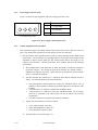
1 drive connection
HA
(Host adaptor)
Host
ATA interface
AT bus
(Host interface)
Figure 2.2
2.2.3
Disk drive
1 drive system configuration
2 drives connection
HA
(Host adaptor)
Host
Disk drive #0
AT bus
(Host interface)
Disk drive #1
ATA interface
Note:
When the drive that is not conformed to ATA is connected to the disk drive is above
configuration, the operation is not guaranteed.
Figure 2.3
2 drives configuration
C141-E106-01EN
2-3
,03257$17
+$ KRVW DGDSWHU FRQVLVWV RI DGGUHVV GHFRGHU GULYHU DQG UHFHLYHU
$7$ LV DQ DEEUHYLDWLRQ RI $7 DWWDFKPHQW 7KH GLVN GULYH LV
FRQIRUPHGWRWKH$7$LQWHUIDFH
$W KLJK VSHHG GDWD WUDQVIHU 3,2 PRGH PRGH '0$ PRGH RU
XOWUD '0$ PRGH RFFXUUHQFH RI ULQJLQJ RU FURVVWDON RI WKH VLJQDO
OLQHV$7EXVEHWZHHQWKH+$DQGWKHGLVNGULYHPD\EHDJUHDWFDXVH
RI WKH REVWUXFWLRQ RI V\VWHP UHOLDELOLW\ 7KXV LW LV QHFHVVDU\ WKDW WKH
FDSDFLWDQFH RI WKH VLJQDO OLQHV LQFOXGLQJ WKH +$ DQG FDEOH GRHV QRW
H[FHHG WKH $7$ $7$ DQG $7$ VWDQGDUG DQG WKH FDEOH OHQJWK
EHWZHHQWKH+$DQGWKHGLVNGULYHVKRXOGEHDVVKRUWDVSRVVLEOH
&((1
CHAPTER 3
3.1
INSTALLATION CONDITIONS
3.1
Dimensions
3.2
Handling Cautions
3.3
Mounting
3.4
Cable Connections
3.5
Jumper Settings
Dimensions
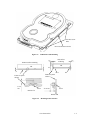
Figure 3.1 illustrates the dimensions of the disk drive and positions of the mounting screw holes.
All dimensions are in mm.
C141-E106-01EN
3-1
Figure 3.1
3-2
Dimensions
C141-E106-01EN
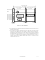
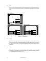
+DQGOLQJ&DXWLRQV
3OHDVHNHHSWKHIROORZLQJFDXWLRQVDQGKDQGOHWKH+''XQGHUWKHVDIHW\HQYLURQPHQW
*HQHUDOQRWHV
(6'PDW
:ULVWVWUDS
6KRFNDEVRUELQJPDW
8VHWKH:ULVWVWUDS
3ODFHWKHVKRFNDEVRUELQJPDWRQWKH
RSHUDWLRQWDEOHDQGSODFH(6'PDWRQLW
'RQRWKLW+''HDFKRWKHU
'RQRWVWDFNZKHQFDUU\LQJ
'RQRWSODFH+''YHUWLFDOO\
WRDYRLGIDOOLQJGRZQ
)LJXUH
'RQRWGURS
+DQGOLQJFDXWLRQV
,QVWDOODWLRQ
3OHDVHXVHWKHGULYHURIDORZLPSDFWZKHQ\RXXVHDQHOHFWULFGULYHU
+''LVRFFDVLRQDOO\GDPDJHGE\WKHLPSDFWRIWKHGULYHU
3OHDVHREVHUYHWKHWLJKWHQLQJWRUTXHRIWKHVFUHZVWULFWO\
81&±±±±±±±0D[1±P.J±FP
5HFRPPHQGHGHTXLSPHQWV
(6'
6KRFN
&RQWHQWV
:ULVWVWUDS
(6'PDW
/RZVKRFNGULYHU
0RGHO
-;
'(6$6.
66
&((1
0DNHU
680,72020
&20.</(
+,26
3.3
Mounting
(1)
Direction
Figure 3.3 illustrates normal direction for the disk drive. The disk drives can be mounted in any
direction.
Horizontal mounting with the PCB facing down
Figure 3.3
(2)
Direction
Frame
The disk enclosure (DE) body is connected to signal ground (SG) and the mounting frame is also
connected to signal ground. These are electrically shorted.
Note:
Use No.6-32UNC screw for the mounting screw and the screw length should satisfy the
specification in Figure 3.5.
(3)
Limitation of side-mounting
When the disk drive is mounted using the screw holes on both side of the disk drive, use two
screw holes shown in Figure 3.4.
Do not use the center hole. For screw length, see Figure 3.5.
3-4
C141-E106-01EN
Use these screw
holes
Do not use this screw holes
Figure 3.4
Limitation of side-mounting
Side surface
mounting
2.5
Bottom surface mounting
2.5
DE
DE
2.5
2
PCA
A
Frame of system
cabinet
B
Frame of system
cabinet
4.5 or
less
Screw
Screw
5.0 or less
Details of A
Details of B
Figure 3.5
Mounting frame structure
C141-E106-01EN
3-5
(4)
Ambient temperature
The temperature conditions for a disk drive mounted in a cabinet refer to the ambient
temperature at a point 3 cm from the disk drive. Pay attention to the air flow to prevent the DE
surface temperature from exceeding 60°C.
Provide air circulation in the cabinet such that the PCA side, in particular, receives sufficient
cooling. To check the cooling efficiency, measure the surface temperatures of the DE.
Regardless of the ambient temperature, this surface temperature must meet the standards listed in
Table 3.1. Figure 3.6 shows the temperature measurement point.
1
Figure 3.6
Table 3.1
Surface temperature measurement points and standard values
No.
1
3-6
Surface temperature measurement points
Measurement point
DE cover
Temperature
60°C max
C141-E106-01EN
(5)
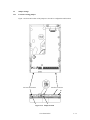
Service area
Figure 3.7 shows how the drive must be accessed (service areas) during and after installation.
- Mounting screw hole
[Q side]
- Mounting screw hole
[P side]
- Cable connection
- Mode setting switches
[R side]
- Mounting screw hole
Figure 3.7
(6)
Service area
External magnetic fields
Avoid mounting the disk drive near strong magnetic sources such as loud speakers. Ensure that
the disk drive is not affected by external magnetic fields.
C141-E106-01EN
3-7
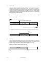
&DEOH&RQQHFWLRQV
'HYLFHFRQQHFWRU
7KH GLVN GULYH KDV WKH FRQQHFWRUV DQG WHUPLQDOV OLVWHG EHORZ IRU FRQQHFWLQJ H[WHUQDO GHYLFHV
)LJXUHVKRZVWKHORFDWLRQVRIWKHVHFRQQHFWRUVDQGWHUPLQDOV
x
x
3RZHUVXSSO\FRQQHFWRU&1
$7$LQWHUIDFHFRQQHFWRU&1
3RZHUVXSSO\
FRQQHFWRU&1
0RGH
6HWWLQJ
3LQV
$7$
LQWHUIDFH
FRQQHFWRU
)LJXUH
&RQQHFWRUORFDWLRQV
&((1
&DEOHFRQQHFWRUVSHFLILFDWLRQV
7DEOHOLVWVWKHUHFRPPHQGHGVSHFLILFDWLRQVIRUWKHFDEOHFRQQHFWRUVIRU+RVWV\VWHPWKDWGR
QRWVXSSRUW8OWUD'0$PRGHVJUHDWHUWKDQPRGH
)RU+RVWV\VWHPWKDWVXSSRUW8OWUD'0$PRGHVJUHDWHUWKDQPRGHLWLVUHFRPPHQGHGWRXVHWKH
FRQGXFWRUFDEOHDVVHPEO\7KHFRQGXFWRUFDEOHDVVHPEO\LVPDQXIDFWXUHGE\$03RU0
7DEOH
&DEOHFRQQHFWRUVSHFLILFDWLRQV
1DPH
$7$LQWHUIDFHFDEOH
SLQ&1
3RZHUVXSSO\FDEOH
&1
0RGHO
0DQXIDFWXUHU
&DEOHVRFNHW
FORVHGHQGW\SH
)&1%$8%
)XMLWVX
&DEOHVRFNHW
WKURXJKHQGW\SH
)&1%$82
)XMLWVX
&DEOHVRFNHWKRXVLQJ
$03
&RQWDFW
$03
1RWH
7KHFDEOHRIWZLVWHGSDLUVDQGQHLJKERULQJOLQHVHSDUDWHGLQGLYLGXDOO\LVQRWDOORZHGWRXVHIRU
WKH KRVW LQWHUIDFH FDEOH ,W LV EHFDXVH WKDW WKH ORFDWLRQ RI VLJQDO OLQHV LQ WKHVH FDEOHV LV QRW
IL[HGDQGVRWKHSUREOHPRQWKHFURVVWDONDPRQJVLJQDOOLQHVPD\RFFXU
,WLVUHFRPPHQGHGWRXVHWKHULEERQFDEOHIRU$7$LQWHUIDFHWKDWFDEOHOHQJWKLVOHVVWKDQ
FPLQFKDQGFDEOHFDSDFLWDQFHLVOHVVWKDQSLFRIDUDG$OVRLWLVUHFRPPHQGHGWRXVH
$:*SRZHUVXSSO\FDEOH
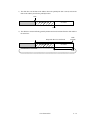
'HYLFHFRQQHFWLRQ
)LJXUHVKRZVKRZWRFRQQHFWWKHGHYLFHV
$7$LQWHUIDFHFDEOH
3RZHUVXSSO\FDEOH
'LVN'ULYH
+RVWV\VWHP
'&
SRZHUVXSSO\
'LVN'ULYH
)LJXUH
&DEOHFRQQHFWLRQV
&((1
3.4.4
Power supply connector (CN1)
Figure 3.10 shows the pin assignment of the power supply connector (CN1).
1
2
3
4
1
+12VDC
2
+12V RETURN
3
+5V RETURN
4
+5VDC
(Viewed from cable side)
Figure 3.10 Power supply connector pins (CN1)
3.4.5
System configuration for Ultra DMA
Host system that support Ultra DMA transfer modes greater than mode 2 shall not share I/O
ports. They shall provide separate drivers and separate receivers for each cable.
a) The 80-conductor cable assemblies shall be used for systems operating at Ultra DMA modes
greater than 2. The 80-coductor cable assemblies may be used in place of 40-conductor cable
assemblies to improve signal quality for data transfer modes that do not require an 80conductor cable assembly. And the 80-conductor cable assembly shall meet the following
specifications.
1)
The assembly utilizes a fine pitch cable to double the number of conductors available to
the 40-pin connector. The grounds assigned by the interface are common with the
additional 40 conductors to provide a ground between each signal line and provide the
effect of a common ground plane.
2)
The cable assembly may contain up to 3 connectors which shall be uniquely colored as
follows. All connectors shall have position 20 blocked.
•
•
•
•
3)
Typical cable characteristics are shown as follows.
•
•
•
4)
3 - 10
The System Board Connector shall have a Blue base and Black retainer. Pin 34
(PDIAG-: CBLID-) shall be connected to ground and shall not be wired to the cable
assembly.
Connector Device “0” shall have a Black base and Black retainer.
Connector Device “1” shall have a Gray base and Black retainer. Pin 28 (CSEL)
shall not be connected to the cable (contact 28 may be removed to meet this
requirement).
The cable assembly may be printed with connector identifiers.
Cable: AWG 30 (pitch: 0.635 mm)
Single Ended impedance: typical 80 Ω.
Cable capacitance: typical 57 pF/m
The dimensions are shown in Figure 3.11.
C141-E106-01EN
254.0 to 457.2 mm
(10 to 18 inch)
127.0 to 304.8 mm
101.6 to 152.4 mm
(5 to 12 inch)
(4 to 6 inch)
Pin 40 (Ground)
open
Pin 34
Pin 34 contact
(PDIAG-:CBLID- signal)
Pin 30 (Ground)
Pin 26 (Ground)
Pin 24 (Ground)
Pin 22 (Ground)
Pin 19 (Ground)
Symbolizes Pin 34
Conductor being cut
Position 1
Pin 2 (Ground)
System Board
Connector
Connector 1
Connector 2
Figure 3.11 Cable configuration
b) Host system that do not support Ultra DMA modes greater than mode 2 shall not connect to
the PDIAG-:CBLID- signal.
c) Host system that do support Ultra DMA modes greater than mode 2 shall either connect
directly to the device without using a cable assembly, or determine the cable assembly type.
Determining the cable assembly type may be done either by the host sensing the condition of
the PDIAG-:CBLID- signal (see Figure 3.12), or by relying on information from the device
(see Figure 3.13). Hosts that rely on information from the device shall have a 0.047 µF
capacitor connected from the PDIAG-:CBLID- signal to ground. The tolerance on this
capacitor shall be 20% or less.
C141-E106-01EN
3 - 11
Host detected CBLID- below VIL
Host detected CBLID- above VIH
open
PDIAG-: CBLID- conductor
Host
Device 1
Device 0
PDIAG-: CBLID- conductor
Host
with 40-conductor cable
Device 1
Device 0
with 80-conductor cable
Figure 3.12 Cable type detection using CBLID- signal
(Host sensing the condition of the CBLID- signal)
IDENTIFY DEVICE information
word 93 bit13:1
Device detected CBLID- above VIH
open PDIAG-:CBLID- conductor
IDENTIFY DEVICE information
word 93 bit13:0
Device detected CBLID- below VIL
PDIAG-:CBLID- conductor
0.047 µF
±10% or
±20%
Host
0.047 µF
±10% or
±20%
Device 1
Device 0
Host
with 40-conductor cable
Device 1
with 80-conductor cable
Figure 3.13 Cable type detection using IDENTIFY DEVICE data
(Device sensing the condition of the CBLID- signal)
3 - 12
C141-E106-01EN
Device 0
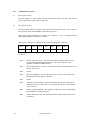
-XPSHU6HWWLQJV
/RFDWLRQRIVHWWLQJMXPSHUV
)LJXUHVKRZVWKHORFDWLRQRIWKHMXPSHUVWRVHOHFWGULYHFRQILJXUDWLRQDQGIXQFWLRQV
'&3RZHU&RQQHFWRU
,QWHUIDFH&RQQHFWRU
)LJXUH -XPSHUORFDWLRQ
&((1
3.5.2
Factory default setting
Figure 3.15 shows the default setting position at the factory. (Master device setting)
DC Power Connector
Interface Connector
Figure 3.15 Factory default setting
3.5.3
Jumper configuration
(1)
Device type
Master device (device #0) or slave device (device #1) is selected.
2
4 6 8
2
4 6 8
= shorted
1
3 5 7 9
(a) Master device
1
3 5 7 9
(b) Slave device
Figure 3.16 Jumper setting of master or slave device
Note:
When the device type is set by the jumper on the device, the device should not be configured
for cable selection.
(2)
Cable Select (CSEL)
In Cable Select mode, the device can be configured either master device or slave device. For use
of Cable Select function, Unique interface cable is needed.
3 - 14
C141-E106-01EN
2
4 6 8
1
3 5 7 9
CSEL connected to the interface cable selection
can be done by the special interface cable.
Figure 3.17 Jumper setting of Cable Select
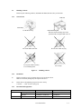
Figures 3.18 and 3.19 show examples of cable selection using unique interface cables.
By connecting the CSEL of the master device to the CSEL Line (conductor) of the cable and
connecting it to ground further, the CSEL is set to low level. The device is identified as a master
device. At this time, the CSEL of the slave device does not have a conductor. Thus, since the
slave device is not connected to the CSEL conductor, the CSEL is set to high level. The device is
identified as a slave device.
CSEL conductor
Open
GND
Host system
Master device
Slave device
Figure 3.18 Example (1) of Cable Select
CSEL conductor
GND
Host system
Open
Slave device
Master device
Figure 3.19 Example (2) of Cable Select
C141-E106-01EN
3 - 15
(3)
Special jumper settings
(a) 2.1 GB clip (Limit capacity to 2.1 GB)
If the drive cannot be recognized by system with legacy BIOS’s which do not allow single
volume sizes greater than approximately 2.1 GB, the following jumper settings should be
applied.
2
4 6 8
2
4 6 8
2
4 6 8
1
3 5 7 9
1
3 5 7 9
1
3 5 7 9
Master Device
Model
Slave Device
Cable Select
No. of cylinders
No. of heads
No. of sectors
MPF3102AH
4,092
16
63
MPF3153AH
4,092
16
63
MPF3204AH
4,092
16
63
(b) Slave present
If the slave device does not use the Device Active/Slave Present (DASP–) signal to indicate
its presence, the device is configured as a Master with slave present when the following
jumper settings is applied.
2
4 6 8
1
3 5 7 9
Slave present
3 - 16
C141-E106-01EN
CHAPTER 4
THEORY OF DEVICE OPERATION
4.1
Outline
4.2
Subassemblies
4.3
Circuit Configuration
4.4
Power-on sequence
4.5
Self-calibration
4.6
Read/write Circuit
4.7
Servo Control
This chapter explains basic design concepts of the disk drive. Also, this chapter explains subassemblies of
the disk drive, each sequence, servo control, and electrical circuit blocks.
4.1
Outline
This chapter consists of two parts. First part (Section 4.2) explains mechanical assemblies of the
disk drive. Second part (Sections 4.3 through 4.7) explains a servo information recorded in the
disk drive and drive control method.
4.2
Subassemblies
The disk drive consists of a disk enclosure (DE) and printed circuit assembly (PCA).
The DE contains all movable parts in the disk drive, including the disk, spindle, actuator,
read/write head, and air filter. For details, see Subsections 4.2.1 to 4.2.5.
The PCA contains the control circuits for the disk drive. The disk drive has one PCA. For
details, see Sections 4.3.
4.2.1
Disk
The DE contains the disks with an outer diameter of 95 mm. The MPF3102AH has 1 disk, and
MPF3153AH and MPF3204AH have 2 disk.
The head contacts the disk each time the disk rotation stops; the life of the disk is 40,000 contacts
or more.
Servo data is recorded on each cylinder (total 72). Servo data written at factory is read out by the
read/write head. For servo data, see Section 4.7.
C141-E106-01EN
4-1
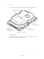
+HDG
)LJXUHVKRZVWKHUHDGZULWHKHDGVWUXFWXUHV7KH1XPHUDOVWRLQGLFDWHUHDGZULWHKHDGV
7KHVH KHDGV DUH UDLVHG IURP WKH GLVN VXUIDFH DV WKH VSLQGOH PRWRU DSSURDFKHV WKH UDWHG URWDWLRQ
VSHHG
03)$70RGHO
$FWXDWRU
6SLQGOH
03)$70RGHO
03)$70RGHO
$FWXDWRU
6SLQGOH
$FWXDWRU
6SLQGOH
)LJXUH
+HDGVWUXFWXUH
6SLQGOH
7KH VSLQGOH FRQVLVWV RI D GLVN VWDFN DVVHPEO\ DQG VSLQGOH PRWRU 7KH GLVN VWDFN DVVHPEO\ LV
DFWLYDWHGE\WKHGLUHFWGULYHVHQVRUOHVV'&VSLQGOHPRWRUZKLFKKDVDVSHHGRIUSP7KH
VSLQGOHLVFRQWUROOHGZLWKGHWHFWLQJD3+$6(VLJQDOJHQHUDWHGE\FRXQWHUHOHFWURPRWLYHYROWDJHRI
WKH VSLQGOH PRWRU DW VWDUWLQJ $IWHU WKDW WKH URWDWLRQDO VSHHG LV NHSW ZLWK GHWHFWLQJ D VHUYR
LQIRUPDWLRQ
$FWXDWRU
7KH DFWXDWRU FRQVLVWV RI D YRLFH FRLO PRWRU 9&0 DQG D KHDG FDUULDJH 7KH 9&0 PRYHV WKH
KHDGFDUULDJHDORQJWKHLQQHURURXWHUHGJHRIWKHGLVN7KHKHDGFDUULDJHSRVLWLRQLVFRQWUROOHG
E\ IHHGLQJ EDFN WKH GLIIHUHQFH RI WKH WDUJHW SRVLWLRQ WKDW LV GHWHFWHG DQG UHSURGXFHG IURP WKH
VHUYRLQIRUPDWLRQUHDGE\WKHUHDGZULWHKHDG
&((1
4.2.5
Air filter
There are two types of air filters: a breather filter and a circulation filter.
The breather filter makes an air in and out of the DE to prevent unnecessary pressure around the
spindle when the disk starts or stops rotating. When disk drives are transported under conditions
where the air pressure changes a lot, filtered air is circulated in the DE.
The circulation filter cleans out dust and dirt from inside the DE. The disk drive cycles air
continuously through the circulation filter through an enclosed loop air cycle system operated by
a blower on the rotating disk.
C141-E106-01EN
4-3
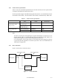
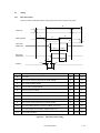
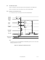
&LUFXLW&RQILJXUDWLRQ
)LJXUHVKRZVWKHGLVNGULYHFLUFXLWFRQILJXUDWLRQ
5HDGZULWHFLUFXLW
7KHUHDGZULWH FLUFXLW FRQVLVWV RI WZR /6,V UHDGZULWH SUHDPSOLILHU 3UH$03 DQG UHDG FKDQQHO
5'&
7KH3UH$03FRQVLVWVRIWKHZULWHFXUUHQWVZLWFKFLUFXLWWKDWIORZVWKHZULWHFXUUHQWWRWKHKHDG
FRLODQGWKHYROWDJHDPSOLILHUFLUFXLWWKDWDPSOLWXGHVWKHUHDGRXWSXWIURPWKHKHDG
7KH5'&LVWKHUHDGGHPRGXODWLRQFLUFXLWXVLQJWKH([WHQGHG3DUWLDO5HVSRQVH&ODVV(35
DQGFRQWDLQVWKH9LWHUELGHWHFWRUSURJUDPPDEOHORZSDVVILOWHUWDSDGDSWLYHGLJLWDO),5ILOWHU
V\QWKHVL]HUDQGGDWDVHSDUDWRUFLUFXLWV7KH5'&DOVRFRQWDLQVWKHJURXSFRGHGUHFRUGLQJ
*&5HQFRGHUDQGGHFRGHUDQGVHUYRGHPRGXODWLRQFLUFXLW
6HUYRFLUFXLW
7KH SRVLWLRQ DQG VSHHG RI WKH YRLFH FRLO PRWRU DUH FRQWUROOHG E\ FORVHGORRS VHUYR XVLQJ WKH
VHUYR LQIRUPDWLRQ UHFRUGHG RQ WKH GDWD VXUIDFH 7KH VHUYR LQIRUPDWLRQ LV DQ DQDORJ VLJQDO
FRQYHUWHGWRGLJLWDOIRUSURFHVVLQJE\D038DQGWKHQUHFRQYHUWHGWRDQDQDORJVLJQDOIRUFRQWURO
RIWKHYRLFHFRLOPRWRU
6SLQGOHPRWRUGULYHUFLUFXLW
7KHFLUFXLWPHDVXUHVWKHLQWHUYDORID3+$6(VLJQDOJHQHUDWHGE\FRXQWHUHOHFWURPRWLYHYROWDJH
RIDPRWRURUVHUYRPDUNDWWKH038DQGFRQWUROVWKHPRWRUVSHHGFRPSDULQJWDUJHWVSHHG
&RQWUROOHUFLUFXLW
0DMRUIXQFWLRQVDUHOLVWHGEHORZ
x
x
x
x
x
x
'DWDEXIIHUPDQDJHPHQW
$7$LQWHUIDFHFRQWURODQGGDWDWUDQVIHUFRQWURO
6HFWRUIRUPDWFRQWURO
'HIHFWPDQDJHPHQW
(&&FRQWURO
(UURUUHFRYHU\DQGVHOIGLDJQRVLV
&((1
$7$
,QWHUIDFH
3ULQWHG&LUFXLW%RDUG$VVHPEO\
'DWD%XIIHU
'5$0
+'&
+DUG
'LVN
&RQWUROOHU
)ODVK520
)520
0%%!
+'&038
0&8
0LFUR
&RQWUROOHU8QLW
5HVRQDWRU
0+]
5HDG&KDQQHO
5'&
6HUYR
9&063,1'/(
&RQWUROOHU
&,55866+
69&
+$)+
',6.
9&0
9RLFH&RLO0RWRU
7HPS
6HQVRU
+($'
5HDG:ULWH
+HDG$VVHPEO\
630
6SLQGOH0RWRU
USP
5HDG:ULWH
3UHDPSOLILHU
65
)3&
'LVN(QFORVXUH
)LJXUH
03)[[[$+%ORFNGLDJUDP
&((1
4.4
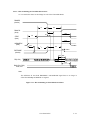
Power-on Sequence
Figure 4.3 describes the operation sequence of the disk drive at power-on.
described below.
The outline is
a) After the power is turned on, the disk drive executes the MPU bus test, internal register
read/write test, and work RAM read/write test. When the self-diagnosis terminates
successfully, the disk drive starts the spindle motor.
b) The disk drive executes self-diagnosis (data buffer read/write test) after enabling response to
the ATA bus.
c) After confirming that the spindle motor has reached rated speed, the disk drive releases the
heads from the actuator magnet lock mechanism by applying current to the VCM. This
unlocks the heads which are parked at the inner circumference of the disks.
d) The disk drive positions the heads onto the SA area and reads out the system information.
e) The disk drive executes self-seek-calibration. This collects data for VCM torque and
mechanical external forces applied to the actuator, and updates the calibrating value.
f) The drive becomes ready. The host can issue commands.
4-6
C141-E106-01EN
Power on
a)
Start
Self-diagnosis 1
• MPU bus test
• Inner register
write/read test
• Work RAM write/read
test
The spindle motor starts.
b)
Self-diagnosis 2
• Data buffer write/read
test
c)
Confirming spindle motor
speed
Release heads from
actuator lock
d)
Initial on-track and read
out of system information
e)
Execute self-calibration
f)
Drive ready state
(command waiting state)
End
Figure 4.3
Power-on operation sequence
C141-E106-01EN
4-7
4.5
Self-calibration
The disk drive occasionally performs self-calibration in order to sense and calibrate mechanical
external forces on the actuator, and VCM torque. This enables precise seek and read/write
operations.
4.5.1
Self-calibration contents
(1)
Sensing and compensating for external forces
The actuator suffers from torque due to the FPC forces and winds accompanying disk revolution.
The torque vary with the disk drive and the cylinder where the head is positioned. To execute
stable fast seek operations, external forces are occasionally sensed.
The firmware of the drive measures and stores the force (value of the actuator motor drive
current) that balances the torque for stopping head stably. This includes the current offset in the
power amplifier circuit and DAC system.
The forces are compensated by adding the measured value to the specified current value to the
power amplifier. This makes the stable servo control.
To compensate torque varying by the cylinder, the disk is divided into 14 areas from the
innermost to the outermost circumference and the compensating value is measured at the
measuring cylinder on each area at factory calibration. The measured values are stored in the SA
cylinder. In the self-calibration, the compensating value is updated using the value in the SA
cylinder.
(2)
Compensating open loop gain
Torque constant value of the VCM has a dispersion for each drive, and varies depending on the
cylinder that the head is positioned. To realize the high speed seek operation, the value that
compensates torque constant value change and loop gain change of the whole servo system due to
temperature change is measured and stored.
For sensing, the firmware mixes the disturbance signal to the position signal at the state that the
head is positioned to any cylinder. The firmware calculates the loop gain from the position
signal and stores the compensation value against to the target gain as ratio.
For compensating, the direction current value to the power amplifier is multiplied by the
compensation value. By this compensation, loop gain becomes constant value and the stable
servo control is realized.
To compensate torque constant value change depending on cylinder, whole cylinders from most
inner to most outer cylinder are divided into 14 partitions at calibration in the factory, and the
compensation data is measured for representative cylinder of each partition. This measured value
is stored in the SA area. The compensation value at self-calibration is calculated using the value
in the SA area.
4-8
C141-E106-01EN
4.5.2
Execution timing of self-calibration
Self-calibration is executed when:
•
•
The power is turned on.
The self-calibration execution timechart of the disk drive specifies self-calibration.
The disk drive performs self-calibration according to the timechart based on the time elapsed
from power-on. The timechart is shown in Table 4.1. After power-on, self-calibration is
performed about every 30 minutes.
Table 4.1
Self-calibration execution timechart
Time elapsed
4.5.3
Time elapsed (accumulated)
1
At power-on
Initial calibration
2
About 30 minutes
About 30 minutes
3
About 30 minutes
About 60 minutes
4
About 30 minutes
About 90 minutes
5
About 30 minutes
About 120 minutes
6
About 30 minutes
About 150 minutes
7
.
.
.
9
Every about 30 minutes
Command processing during self-calibration
If the disk drive receives a command execution request from the host while executing selfcalibration according to the timechart, the disk drive terminates self-calibration and starts
executing the command precedingly. In other words, if a disk read or write service is necessary,
the disk drive positions the head to the track requested by the host, reads or writes data, and
restarts calibration.
This enables the host to execute the command without waiting for a long time, even when the
disk drive is performing self-calibration. The command execution wait time is about maximum
100 ms.
C141-E106-01EN
4-9
5HDGZULWH&LUFXLW
7KHUHDGZULWHFLUFXLWFRQVLVWVRIWKHUHDGZULWHSUHDPSOLILHU3UH$03WKHZULWHFLUFXLWWKHUHDG
FLUFXLWDQGWKHV\QWKHVL]HULQWKHUHDGFKDQQHO5'&
5HDGZULWHSUHDPSOLILHU3UH$03
2QH 3UH$03 LV PRXQWHG RQ WKH )3& 7KH 3UH$03 FRQVLVWV RI DQ FKDQQHO UHDG SUHDPSOLILHU
DQGDZULWHFXUUHQWVZLWFKDQGVHQVHVDZULWHHUURU(DFKFKDQQHOLVFRQQHFWHGWRHDFKGDWDKHDG
7KHKHDG,&VZLWFKHVWKHKHDGVE\WKHVHULDOSRUW6'(16&/.6'$7$7KH,&JHQHUDWHVD
ZULWH HUURU VHQVH VLJQDO :86 ZKHQ D ZULWH HUURU RFFXUV GXH WR KHDG VKRUW WR *1' KHDG
GLVFRQQHFWLRQ
:ULWHFLUFXLW
7KHZULWHGDWDLVRXWSXWIURPWKHKDUGGLVNFRQWUROOHU+'&ZLWKWKH15=GDWDIRUPDWDQGVHQW
WRWKHHQFRGHUFLUFXLWLQWKH5'&ZLWKV\QFKURQL]LQJZLWKWKHZULWHFORFN7KH15=ZULWHGDWDLV
FRQYHUWHGIURPELWVGDWDWRELWVGDWDE\WKHHQFRGHUFLUFXLWWKHQVHQWWRWKH3UH$03DQG
WKHGDWDLVZULWWHQRQWRWKHPHGLD
*&5
7KHGLVNGULYHFRQYHUWVGDWDXVLQJWKHJURXSFRGHGUHFRUGLQJ*&5DOJRULWKP
:ULWHSUHFRPSHQVDWLRQ
:ULWHSUHFRPSHQVDWLRQFRPSHQVDWHVGXULQJDZULWHSURFHVVIRUZULWHQRQOLQHDULW\JHQHUDWHGDW
UHDGLQJ
&((1
5HDGFLUFXLW
7KHKHDGUHDGVLJQDOIURPWKH3UH$03LVUHJXODWHGE\WKHYDULDEOHJDLQDPSOLILHU9*$FLUFXLW
7KHQWKHRXWSXWLVFRQYHUWHGLQWRWKHVDPSOHGUHDGGDWDSXOVHE\WKHSURJUDPPDEOHILOWHUFLUFXLW
DQGWKHDGDSWLYHHTXDOL]HUFLUFXLW7KLVFORFNVLJQDOLVFRQYHUWHGLQWRWKH15=GDWDE\WKH
*&5GHFRGHUFLUFXLWEDVHGRQWKHUHDGGDWDPD[LPXPOLNHOLKRRGGHWHFWHGE\WKH9LWHUELGHWHFWLRQ
FLUFXLWWKHQLVVHQWWRWKH+'&
9*$FLUFXLW
7KH9*$FLUFXLWDXWRPDWLFDOO\UHJXODWHVWKHRXWSXWDPSOLWXGHWRDFRQVWDQWYDOXHHYHQZKHQWKH
LQSXWDPSOLWXGHOHYHOIOXFWXDWHV7KH9*$RXWSXWLVPDLQWDLQHGDWDFRQVWDQWOHYHOHYHQZKHQWKH
KHDGRXWSXWIOXFWXDWHVGXHWRWKHKHDGFKDUDFWHULVWLFVRURXWHULQQHUKHDGSRVLWLRQV
3URJUDPPDEOHILOWHU
7KH SURJUDPPDEOH ILOWHU FLUFXLW KDV D ORZSDVV ILOWHU IXQFWLRQ WKDW HOLPLQDWHV XQQHFHVVDU\ KLJK
IUHTXHQF\QRLVHFRPSRQHQWDQGDKLJKIUHTXHQF\ERRVWXSIXQFWLRQWKDWHTXDOL]HVWKHZDYHIRUP
RIWKHUHDGVLJQDO
&XWRIIIUHTXHQF\RIWKHORZSDVVILOWHUDQGERRVWXSJDLQDUHFRQWUROOHGIURPHDFK'$&FLUFXLWLQ
UHDGFKDQQHOE\DQLQVWUXFWLRQRIWKHSDUDOOHOGDWDVLJQDOIURP03807KH038RSWLPL]HV
WKHFXWRIIIUHTXHQF\DQGERRVWXSJDLQDFFRUGLQJWRWKHWUDQVIHUIUHTXHQF\RIHDFK]RQH
$GDSWLYHHTXDOL]HUFLUFXLW
7KLVFLUFXLWLVWDSDGDSWLYHGLJLWDO),5ILOWHUFLUFXLWWKDWFRVLQHHTXDOL]HVWKHKHDGUHDGVLJQDOWR
WKH([WHQGHG3DUWLDO5HVSRQVH&ODVV(35ZDYHIRUP
9LWHUELGHWHFWLRQFLUFXLW
7KHGLJLWDOGDWDRXWSXWIURPWKHDGDSWLYHHTXDOL]HUFLUFXLWLVVHQWWRWKH9LWHUELGHWHFWLRQFLUFXLW
7KH9LWHUELGHWHFWLRQFLUFXLWGHPRGXODWHVGDWDDFFRUGLQJWRWKHVXUYLYRUSDWKVHTXHQFH
'DWDVHSDUDWRUFLUFXLW
7KH GDWD VHSDUDWRU FLUFXLW JHQHUDWHV FORFNV LQ V\QFKURQL]DWLRQ ZLWK WKH RXWSXW RI WKH DGDSWLYH
HTXDOL]HU FLUFXLW 7R ZULWH GDWD WKH 9)2 FLUFXLW JHQHUDWHV FORFNV LQ V\QFKURQL]DWLRQ ZLWK WKH
FORFNVLJQDOVIURPDV\QWKHVL]HU
*&5GHFRGHU
7KLVFLUFXLWFRQYHUWVWKHELWVUHDGGDWDLQWRWKHELWV15=GDWD
&((1
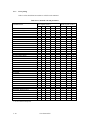
6\QWKHVL]HUFLUFXLW
7KH GULYH XVHV FRQVWDQW GHQVLW\ UHFRUGLQJ WR LQFUHDVH WRWDO FDSDFLW\ 7KLV LV GLIIHUHQW IURP WKH
FRQYHQWLRQDO PHWKRG RI UHFRUGLQJ GDWD ZLWK D IL[HG GDWD WUDQVIHU UDWH DW DOO GDWD DUHD ,Q WKH
FRQVWDQWGHQVLW\UHFRUGLQJPHWKRGGDWDDUHDLVGLYLGHGLQWR]RQHVE\UDGLXVDQGWKHGDWDWUDQVIHU
UDWHLVVHWVRWKDWWKHUHFRUGLQJGHQVLW\RIWKHLQQHUF\OLQGHURIHDFK]RQHLVQHDUO\FRQVWDQW7KH
GULYH GLYLGHV GDWD DUHD LQWR ]RQHV WR VHW WKH GDWD WUDQVIHU UDWH 7DEOH GHVFULEHV WKH GDWD
WUDQVIHUUDWHDQGUHFRUGLQJGHQVLW\%3,RIHDFK]RQH
7DEOH
=RQH
&\OLQGHU
7UDQVIHUUDWH
>0%V@
=RQH
&\OLQGHU
7UDQVIHUUDWH
>0%V@
7UDQVIHUUDWHRIHDFK]RQH
WR
WR
WR
WR
WR
WR
WR
WR
WR
WR
WR
WR
WR
WR
WR
7KH038WUDQVIHUVWKHGDWDWUDQVIHUUDWHVHWXSGDWDWRWKH5'&WKDWLQFOXGHVV\QWKHVL]HUFLUFXLWWR
FKDQJHWKHGDWDWUDQVIHUUDWH
6HUYR&RQWURO
7KHDFWXDWRUPRWRUDQGWKHVSLQGOHPRWRUDUHVXEPLWWHGWRVHUYRFRQWURO7KHDFWXDWRUPRWRULV
FRQWUROOHGIRUPRYLQJDQGSRVLWLRQLQJWKHKHDGWRWKHWUDFNFRQWDLQLQJWKHGHVLUHGGDWD7RWXUQ
WKHGLVNDWDFRQVWDQWYHORFLW\WKHDFWXDWRUPRWRULVFRQWUROOHGDFFRUGLQJWRWKHVHUYRGDWDWKDWLV
ZULWWHQRQWKHGDWDVLGHEHIRUHKDQG
&((1
4.7.1
Servo control circuit
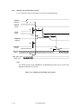
Figure 4.4 is the block diagram of the servo control circuit.
functions of the blocks:
The following describes the
(1)
MPU
Head
(2)
Servo
burst
capture
(3)
(4)
DSP
unit
ADC
SVC
(5)
DAC
VCM current
P.
Amp.
CSR
Position Sense
VCM
(6)
Spindle
motor
control
CSR: Current Sense Resistor
VCM: Voice Coil Motor
Figure 4.4
(1)
(7)
Driver
Spindle
motor
Block diagram of servo control circuit
Microprocessor unit (MPU)
The MPU includes DSP unit, etc., and the MPU starts the spindle motor, moves the heads to the
reference cylinders, seeks the specified cylinder, and executes calibration according to the
internal operations of the MPU.
The major internal operations are listed below.
a. Spindle motor start
Starts the spindle motor and accelerates it to normal speed when power is applied.
b. Move head to reference cylinder
Drives the VCM to position the head at the any cylinder in the data area. The logical initial
cylinder is at the outermost circumference (cylinder 0).
C141-E106-01EN
4 - 13
c. Seek to specified cylinder
Drives the VCM to position the head to the specified cylinder.
d. Calibration
Senses and stores the thermal offset between heads and the mechanical forces on the actuator,
and stores the calibration value.
Servo frame
(72 servo frames per revolution)
Figure 4.5
4 - 14
Physical sector servo configuration on disk surface
C141-E106-01EN
(2)
Servo burst capture circuit
The four servo signals can be synchronously detected by the DEMOD signal (internal), full-wave
rectified integrated.
(3)
A/D converter (ADC)
The A/D converter (ADC) receives the servo signals are integrated, converts them to digital, and
transfers the digital signal to the DSP unit.
(4)
D/A converter (DAC)
The D/A converter (DAC) converts the VCM drive current value (digital value) calculated by the
DSP unit into analog values and transfers them to the power amplifier.
(5)
Power amplifier
The power amplifier feeds currents, corresponding to the DAC output signal voltage to the VCM.
(6)
Spindle motor control circuit
The spindle motor control circuit controls the sensor-less spindle motor. This circuit detects
number of revolution of the motor by the interrupt generated periodically, compares with the
target revolution speed, then flows the current into the motor coil according to the differentiation
(aberration).
(7)
Driver circuit
The driver circuit is a power amplitude circuit that receives signals from the spindle motor
control circuit and feeds currents to the spindle motor.
(8)
VCM current sense resistor (CSR)
This resistor controls current at the power amplifier by converting the VCM current into voltage
and feeding back.
C141-E106-01EN
4 - 15
4.7.2
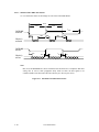
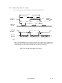
Data-surface servo format
Figure 4.5 describes the physical layout of the servo frame. The three areas indicated by (1) to
(3) in Figure 4.6 are described below.
(1)
Inner guard band
The head is in contact with the disk in this space when the spindle starts turning or stops, and the
rotational speed of the spindle can be controlled on this cylinder area for head moving.
(2)
Data area
This area is used as the user data area and SA area.
(3)
Outer guard band
This area is located at outer position of the user data area, and the rotational speed of the spindle
can be controlled on this cylinder area for head moving.
4.7.3
Servo frame format
As the servo information, the drive uses the two-phase servo generated from the gray code and
Pos A to D. This servo information is used for positioning operation of radius direction and
position detection of circumstance direction.
The servo frame consists of 5 blocks; write/read recovery, servo mark, gray code, Pos A to D and
PAD. Figure 4.6 shows the servo frame format.
4 - 16
C141-E106-01EN
PV
PV
PV
PV
PV
PV
PV
PV
PV PV
PV PV
PV PV
PV PV
PV PV
PV
PV
6&'
3$
$60
326
$
326
%
326
&
326
'
3$'
660
:55HFRYHU\)LHOG
PV
PV
6HUYR
)UDPH
'$7$
'$7$
6HUYR
)UDPH
PV
)LJXUH
VHUYRIUDPHVLQHDFKWUDFN
:ULWHUHDGUHFRYHU\
7KLVDUHDLVXVHGWRDEVRUEWKHZULWHUHDGWUDQVLHQWDQGWRVWDELOL]HWKH$*&
6HUYRPDUN$60660
7KLVDUHDJHQHUDWHVDWLPLQJIRUGHPRGXODWLQJWKHJUD\FRGHDQGSRVLWLRQGHPRGXODWLQJ3RV$WR
'E\GHWHFWLQJWKHVHUYRPDUN
&((1
(3)
Preamble
This area is used to synchronize with the PLL, which is used to search the SSM by detecting the
ASM.
(4)
Gray code (including index bit)
This area is used as cylinder address. The data in this area is converted into the binary data by
the gray code demodulation circuit.
(5)
Pos A, Pos B, Pos C, Pos D
This area is used as position signals between tracks, and the device control at on-track so that Pos
A level equals to Pos B level.
(6)
PAD
This area is used as a gap between servo and data.
4.7.4
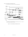
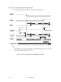
Actuator motor control
The voice coil motor (VCM) is controlled by feeding back the servo data recorded on the data
surface. The MPU fetches the position sense data on the servo frame at a constant interval of
sampling time, executes calculation, and updates the VCM drive current.
The servo control of the actuator includes the operation to move the head to the reference
cylinder, the seek operation to move the head to the target cylinder to read or write data, and the
track-following operation to position the head onto the target track.
(1)
Operation to move the head to the reference cylinder
The MPU moves the head to the reference cylinder when the power is turned. The reference
cylinder is in the data area.
When power is applied the heads are moved from the inner circumference shunt zone to the
normal servo data zone in the following sequence:
a) Micro current is fed to the VCM to press the head against the inner circumference.
b) A current is fed to the VCM to move the head toward the outer circumference.
c) When the servo mark is detected the head is moved slowly toward the outer circumference at
a constant speed.
d) If the head is stopped at the reference cylinder from there. Track following control starts.
4 - 18
C141-E106-01EN
(2)
Seek operation
Upon a data read/write request from the host, the MPU confirms the necessity of access to the
disk. If a read or instruction is issued, the MPU seeks the desired track.
The MPU feeds the VCM current via the D/A converter and power amplifier to move the head.
The MPU calculates the difference (speed error) between the specified target position and the
current position for each sampling timing during head moving. The MPU then feeds the VCM
drive current by setting the calculated result into the D/A converter. The calculation is digitally
executed by the firmware. When the head arrives at the target cylinder, the track is followed.
(3)
Track following operation
Except during head movement to the reference cylinder and seek operation under the spindle
rotates in steady speed, the MPU does track following control. To position the head at the center
of a track, the DSP drives the VCM by feeding micro current. For each sampling time, the VCM
drive current is determined by filtering the position difference between the target position and the
position clarified by the detected position sense data. The filtering includes servo compensation.
These are digitally controlled by the firmware.
4.7.5
Spindle motor control
Hall-less three-phase eight-pole motor is used for the spindle motor, and the 3-phase full/halfwave analog current control circuit is used as the spindle motor driver (called SVC hereafter).
The firmware operates on the MPU manufactured by Fujitsu. The spindle motor is controlled by
sending several signals from the MPU to the SVC. There are three modes for the spindle control;
start mode, acceleration mode, and stable rotation mode.
(1)
Start mode
When power is supplied, the spindle motor is started in the following sequence:
a) After the power is turned on, the MPU sends a signal to the SVC to charge the change pump
capacitor of the SVC. The charged amount defines the current that flows in the spindle
motor.
b) When the charge pump capacitor is charged enough, the MPU sets the SVC to the motor start
mode. Then, a starting current flows into the spindle motor.
c) The SVC generates a phase switching signal by itself, and changes the phase of the current
flowed in the motor in the order of (V-phase to U-phase), (W-phase to U-phase), (W-phase to
V-phase), (U-phase to V-phase), (U-phase to W-phase), and (V-phase to W-phase) (after that,
repeating this order).
d) During phase switching, the spindle motor starts rotating in low speed, and generates a
counter electromotive force. The SVC detects this counter electromotive force and reports to
the MPU using a PHASE signal for speed detection.
e) The MPU is waiting for a PHASE signal. When no phase signal is sent for a specific period,
the MPU resets the SVC and starts from the beginning. When a PHASE signal is sent, the
SVC enters the acceleration mode.
C141-E106-01EN
4 - 19
(2)
Acceleration mode
In this mode, the MPU stops to send the phase switching signal to the SVC. The SVC starts a
phase switching by itself based on the counter electromotive force. Then, rotation of the spindle
motor accelerates. The MPU calculates a rotational speed of the spindle motor based on the
PHASE signal from the SVC, and accelerates till the rotational speed reaches 7,200 rpm. When
the rotational speed reaches 7,200 rpm, the SVC enters the stable rotation mode.
(3)
Stable rotation mode
The MPU calculates a time for one revolution of the spindle motor based on the PHASE signal
from the SVC. The MPU takes a difference between the current time and a time for one
revolution at 7,200 rpm that the MPU already recognized. Then, the MPU keeps the rotational
speed to 7,200 rpm by charging or discharging the charge pump for the different time. For
example, when the actual rotational speed is 7,400 rpm, the time for one revolution is 8.108 ms.
And, the time for one revolution at 7,200 rpm is 8.333 ms. Therefore, the MPU discharges the
charge pump for 0.225 ms × k (k: constant value). This makes the flowed current into the motor
lower and the rotational speed down. When the actual rotational speed is later than 7,200 rpm,
the MPU charges the pump the other way. This control (charging/discharging) is performed
every 1/6 revolution.
4 - 20
C141-E106-01EN
&+$37(5
,17(5)$&(
3K\VLFDO,QWHUIDFH
/RJLFDO,QWHUIDFH
+RVW&RPPDQGV
&RPPDQG3URWRFRO
8OWUD'0$IHDWXUHVHW
7LPLQJ
&((1
5.1
Physical Interface
5.1.1
Interface signals
Table 5.1 shows the interface signals.
Table 5.1
Interface signals
Description
Host
Cable select
Dir
Dev
see note
Chip select 0
Chip select 1
→
CS0–
→
CS1–
Data bus bit 0
↔
DD0
Data bus bit 1
↔
DD1
Data bus bit 2
↔
DD2
Data bus bit 3
↔
DD3
Data bus bit 4
↔
DD4
Data bus bit 5
↔
DD5
Data bus bit 6
↔
DD6
Data bus bit 7
↔
DD7
Data bus bit 8
↔
DD8
Data bus bit 9
↔
DD9
Data bus bit 10
↔
DD10
Data bus bit 11
↔
DD11
Data bus bit 12
↔
DD12
Data bus bit 13
↔
DD13
Data bus bit 14
↔
DD14
Data bus bit 15
↔
DD15
Device active or slave present
see note
DASP–
Device address bit 0
→
DA0
Device address bit 1
→
DA1
Device address bit 2
→
DA2
DMA acknowledge
→
DMA request
←
Interrupt request
←
DMACK–
DMARQ
INTRQ
I/O read
→
DIOR–
DMA ready during Ultra DMA data in bursts
→
HDMARDY–
→
Data strobe during Ultra DMA data out bursts
HSTROBE
I/O ready
←
IORDY
DMA ready during Ultra DMA data out bursts
←
DDMARDY–
Data strobe during Ultra DMA data in bursts
←
DSTROBE
I/O write
→
DIOW–
Stop during Ultra DMA data bursts
→
STOP
Passed diagnostics
see note
PDIAG–
Cable type detection
CBLID–
→
Reset
Note: See signal descriptions
5-2
Acrorym
CSEL
C141-E106-01EN
RESET–
5.1.2
Signal assignment on the connector
Table 5.2 shows the signal assignment on the interface connector.
Table 5.2
Signal assignment on the interface connector
Pin No.
Signal
Pin No.
1
3
5
7
9
11
13
15
17
19
21
23
25
27
29
31
33
35
37
39
RESET–
DATA7
DATA6
DATA5
DATA4
DATA3
DATA2
DATA1
DATA0
GND
DMARQ
DIOW–, STOP
DIOR–, HDMARDY–, HSTROBE
IORDY, DDMARDY–, DSTROBE
DMACK–
INTRQ
DA1
DA0
CS0–
DASP–
2
4
6
8
10
12
14
16
18
20
22
24
26
28
30
32
34
36
38
40
[signal]
RESET–
DATA 0-15
DIOW–, STOP
Signal
GND
DATA8
DATA9
DATA10
DATA11
DATA12
DATA13
DATA14
DATA15
(KEY)
GND
GND
GND
CSEL
GND
reserved
PDIAG–, CBLID–
DA2
CS1–
GND
[I/O]
[Description]
I
Reset signal from the host. This signal is low active and is asserted
for a minimum of 25 µs during power on. The device has a 10 kΩ
pull-up resistor on this signal.
I/O
Sixteen-bit bi-directional data bus between the host and the device.
These signals are used for data transfer
I
DIOW– is the strobe signal asserted by the host to write device
registers or the data port.
DIOW– shall be negated by the host prior to initiation of an Ultra
DMA burst. STOP shall be negated by the host before data is
transferred in an Ultra DMA burst. Assertion of STOP by the host
during an Ultra DMA burst signals the termination of the Ultra
DMA burst.
C141-E106-01EN
5-3
[signal]
5-4
[I/O]
[Description]
DIOR–
I
DIOR– is the strobe signal asserted by the host to read device
registers or the data port.
HDMARDY–
I
HDMARDY– is a flow control signal for Ultra DMA data in bursts.
This signal is asserted by the host to indicate to the device that the
host is ready to receive Ultra DMA data in bursts.
The host may negate HDMARDY- to pause an Ultra DMA data in
burst.
HSTROBE
I
HSTROBE is the data out strobe signal from the host for an Ultra
DMA data out burst. Both the rising and falling edge of HSTROBE
latch the data from DATA 0-15 into the device. The host may stop
generating HSTROBE edges to pause an Ultra DMA data out burst.
INTRQ
O
Interrupt signal to the host.
This signal is negated in the following cases:
– assertion of RESET– signal
– Reset by SRST of the Device Control register
– Write to the command register by the host
– Read of the status register by the host
– Completion of sector data transfer
(without reading the Status register)
When the device is not selected or interrupt is disabled, the INTRQ
Signal shall be in a high impedance state.
CS0–
I
Chip select signal decoded from the host address bus. This signal is
used by the host to select the command block registers.
CS1–
I
Chip select signal decoded from the host address bus. This signal is
used by the host to select the control block registers.
DA 0-2
I
Binary decoded address signals asserted by the host to access task
file registers.
KEY
–
Key pin for prevention of erroneous connector insertion
PIDAG–
I/O
This signal is an input mode for the master device and an output
mode for the slave device in a daisy chain configuration. This signal
indicates that the slave device has been completed self diagnostics.
This signal is pulled up to +5 V through 10 kΩ resistor at each device.
CBLID–
I/O
This signal is used to detect the cable type (80 or 40-conductor
cable) installed in the system. This signal is pulled up to +5 V
through 10 kΩ resistor at each device.
DASP–
I/O
This is a time-multiplexed signal that indicates that the device is
active and a slave device is present.
This signal is pulled up to +5 V through 10 kΩ resistor at each device.
C141-E106-01EN
[signal]
[I/O]
[Description]
IORDY
O
This signal is negated to extend the host transfer cycle of any host
register access (Read or Write) when the device is not ready to respond
to a data transfer request.
DDMARDY–
O
DDMARDY– is a flow control signal for Ultra DMA data out bursts.
This signal is asserted by the device to indicate to the host that the
device is ready to receive Ultra DMA data out bursts. The device may
negate DDMARDY– to pause an Ultra DMA data out burst.
DSTROBE
O
DSTROBE is the data in strobe signal from the device for an Ultra
DMA data in burst. Both the rising and falling edge of DSTROBE
latch the data from DATA 0-15 into the host. The device may stop
generating DSTROBE edges to pause an Ultra DMA data in burst.
CSEL
I
This signal to configure the device as a master or a slave device.
When CSEL signal is grounded, the IDD is a master device.
When CSEL signal is open, the IDD is a slave device.
This signal is pulled up with 10 kΩ resistor.
DMACK–
I
The host system asserts this signal as a response that the host
system receive data or to indicate that data is valid.
DMARQ
O
This signal is used for DMA transfer between the host system and
the device. The device asserts this signal when the device completes
the preparation of DMA data transfer to the host system (at reading)
or from the host system (at writing).
The direction of data transfer is controlled by the IOR- and IOWsignals. In other word, the device negates the DMARQ signal after
the host system asserts the DMACK– signal. When there is another
data to be transferred, the device asserts the DMARQ signal again.
When the DMA data transfer is performed, IOCW16–, CS0– and
CS1- signals are not asserted. The DMA data transfer is a 16-bit
data transfer. The device has a 10 kΩ pull-down resistor on this
signal.
GND
–
Grounded
Note:
"I" indicates input signal from the host to the device.
"O" indicates output signal from the device to the host.
"I/O" indicates common output or bi-directional signal between the host and the device.
C141-E106-01EN
5-5
5.2
Logical Interface
The device can operate for command execution in either address-specified mode; cylinder-headsector (CHS) or Logical block address (LBA) mode. The IDENTIFY DEVICE information
indicates whether the device supports the LBA mode. When the host system specifies the LBA
mode by setting bit 6 in the Device/Head register to 1, HS3 to HS0 bits of the Device/Head
register indicates the head No. under the LBA mode, and all bits of the Cylinder High, Cylinder
Low, and Sector Number registers are LBA bits.
The sector No. under the LBA mode proceeds in the ascending order with the start point of
LBA0 (defined as follows).
LBA0 = [Cylinder 0, Head 0, Sector 1]
Even if the host system changes the assignment of the CHS mode by the INITIALIZE DEVICE
PARAMETER command, the sector LBA address is not changed.
LBA = [((Cylinder No.) × (Number of head) + (Head No.)) × (Number of sector/track)]
+ (Sector No.) – 1
5.2.1
I/O registers
Communication between the host system and the device is done through input-output (I/O)
registers of the device.
These I/O registers can be selected by the coded signals, CS0–, CS1–, and DA0 to DA2 from the
host system. Table 5.3 shows the coding address and the function of I/O registers.
5-6
C141-E106-01EN
Table 5.3
I/O registers
I/O registers
CS0–
CS1–
DA2
DA1
DA0
Read operation
Write operation
Host I/O
address
Command block registers
1
0
0
0
0
Data
Data
X'1F0'
1
0
0
0
1
Error Register
Features
X'1F1'
1
0
0
1
0
Sector Count
Sector Count
X'1F2'
1
0
0
1
1
Sector Number
Sector Number
X'1F3'
1
0
1
0
0
Cylinder Low
Cylinder Low
X'1F4'
1
0
1
0
1
Cylinder High
Cylinder High
X'1F5'
1
0
1
1
0
Device/Head
Device/Head
X'1F6'
1
0
1
1
1
Status
Command
X'1F7'
1
1
X
X
X
(Invalid)
(Invalid)
—
Control block registers
0
1
1
1
0
Alternate Status
Device Control
X'3F6'
0
1
1
1
1
—
—
X'3F7'
Notes:
1.
The Data register for read or write operation can be accessed by 16 bit data bus (DATA0
to DATA15).
2.
The registers for read or write operation other than the Data registers can be accessed by
8 bit data bus (DATA0 to DATA7).
3.
When reading the Drive Address register, bit 7 is high-impedance state.
4.
The LBA mode is specified, the Device/Head, Cylinder High, Cylinder Low, and Sector
Number registers indicate LBA bits 27 to 24, 23 to 16, 15 to 8, and 7 to 0.
C141-E106-01EN
5-7
5.2.2
Command block registers
(1)
Data register (X'1F0')
The Data register is a 16-bit register for data block transfer between the device and the host
system. Data transfer mode is PIO or LBA mode.
(2)
Error register (X'1F1')
The Error register indicates the status of the command executed by the device. The contents of
this register are valid when the ERR bit of the Status register is 1.
This register contains a diagnostic code after power is turned on, a reset , or the EXECUTIVE
DEVICE DIAGNOSTIC command is executed.
[Status at the completion of command execution other than diagnostic command]
Bit 7
Bit 6
Bit 5
Bit 4
Bit 3
Bit 2
Bit 1
Bit 0
ICRC
UNC
X
IDNF
X
ABRT
TK0NF
AMNF
X: Unused
5-8
- Bit 7:
Interface CRC error (ICRC). This bit indicates that an interface CRC error has
occurred during an Ultra DMA data transfer. The content of this bit is not
applicable for Multiword DMA transfers.
- Bit 6:
Uncorrectable Data Error (UNC). This bit indicates that an uncorrectable data error
has been encountered.
- Bit 5:
Unused
- Bit 4:
ID Not Found (IDNF). This bit indicates an error except for, uncorrectable error
and SB not found, and Aborted Command.
- Bit 3:
Unused
- Bit 2:
Aborted Command (ABRT). This bit indicates that the requested command was
aborted due to a device status error (e.g. Not Ready, Write Fault) or the command
code was invalid.
- Bit 1:
Track 0 Not Found (TK0NF). This bit indicates that track 0 was not found during
RECALIBRATE command execution.
- Bit 0:
Address Mark Not Found. This bit indicates that an SB not found error has been
encountered.
C141-E106-01EN
[Diagnostic code]
(3)
X'01':
No Error Detected.
X'02':
HDC Register Compare Error
X'03':
Data Buffer Compare Error.
X'05':
ROM Sum Check Error.
X'80':
Device 1 (slave device) Failed.
Error register of the master device is valid under two devices (master and slave)
configuration. If the slave device fails, the master device posts X’80’ OR (the
diagnostic code) with its own status (X'01' to X'05').
However, when the host system selects the slave device, the diagnostic code of the slave
device is posted.
Features register (X'1F1')
The Features register provides specific feature to a command. For instance, it is used with SET
FEATURES command to enable or disable caching.
(4)
Sector Count register (X'1F2')
The Sector Count register indicates the number of sectors of data to be transferred in a read or
write operation between the host system and the device. When the value in this register is X'00',
the sector count is 256.
When this register indicates X'00' at the completion of the command execution, this indicates
that the command is completed successfully. If the command is not completed successfully, this
register indicates the number of sectors to be transferred to complete the request from the host
system. That is, this register indicates the number of remaining sectors that the data has not been
transferred due to the error.
The contents of this register has other definition for the following commands; INITIALIZE
DEVICE PARAMETERS, FORMAT TRACK, SET FEATURES, IDLE, STANDBY and SET
MULTIPLE MODE.
(5)
Sector Number register (X'1F3')
The contents of this register indicates the starting sector number for the subsequent command.
The sector number should be between X'01' and [the number of sectors per track defined by
INITIALIZE DEVICE PARAMETERS command.
Under the LBA mode, this register indicates LBA bits 7 to 0.
C141-E106-01EN
5-9
(6)
Cylinder Low register (X'1F4')
The contents of this register indicates low-order 8 bits of the starting cylinder address for any
disk-access.
At the end of a command, the contents of this register are updated to the current cylinder
number.
Under the LBA mode, this register indicates LBA bits 15 to 8.
(7)
Cylinder High register (X'1F5')
The contents of this register indicates high-order 8 bits of the disk-access start cylinder address.
At the end of a command, the contents of this register are updated to the current cylinder
number. The high-order 8 bits of the cylinder address are set to the Cylinder High register.
Under the LBA mode, this register indicates LBA bits 23 to 16.
(8)
Device/Head register (X'1F6')
The contents of this register indicate the device and the head number.
When executing INITIALIZE DEVICE PARAMETERS command, the contents of this register
defines "the number of heads minus 1".
5 - 10
Bit 7
Bit 6
Bit 5
Bit 4
Bit 3
Bit 2
Bit 1
Bit 0
X
L
X
DEV
HS3
HS2
HS1
HS0
- Bit 7:
Unused
- Bit 6:
L. 0 for CHS mode and 1 for LBA mode.
- Bit 5:
Unused
- Bit 4:
DEV bit. 0 for the master device and 1 for the slave device.
- Bit 3:
HS3 CHS mode head address 3 (23). LBA bit 27.
- Bit 2:
HS2 CHS mode head address 3 (22). LBA bit 26.
- Bit 1:
HS1 CHS mode head address 3 (21). LBA bit 25.
- Bit 0:
HS0 CHS mode head address 3 (20). LBA bit 24.
C141-E106-01EN
(9)
Status register (X'1F7')
The contents of this register indicate the status of the device. The contents of this register are
updated at the completion of each command. When the BSY bit is cleared, other bits in this
register should be validated within 400 ns. When the BSY bit is 1, other bits of this register are
invalid. When the host system reads this register while an interrupt is pending, it is considered to
be the Interrupt Acknowledge (the host system acknowledges the interrupt). Any pending
interrupt is cleared (negating INTRQ signal) whenever this register is read.
Bit 7
Bit 6
Bit 5
Bit 4
Bit 3
Bit 2
Bit 1
Bit 0
BSY
DRDY
DF
DSC
DRQ
0
0
ERR
- Bit 7:
Busy (BSY) bit. This bit is set whenever the Command register is accessed. Then
this bit is cleared when the command is completed. However, even if a command is
being executed, this bit is 0 while data transfer is being requested (DRQ bit =
1).When BSY bit is 1, the host system should not write the command block
registers. If the host system reads any command block register when BSY bit is 1,
the contents of the Status register are posted. This bit is set by the device under
following conditions:
(a)
Within 400 ns after RESET- is negated or SRST is set in the Device Control
register, the BSY bit is set. The BSY bit is cleared, when the reset process is
completed.
The BSY bit is set for no longer than 15 seconds after the IDD accepts reset.
(b)
Within 400 ns from the host system starts writing to the Command register.
(c)
Within 5 µs following transfer of 512 bytes data during execution of the
READ SECTOR(S), WRITE SECTOR(S), FORMAT TRACK, or WRITE
BUFFER command.
Within 5 µs following transfer of 512 bytes of data and the appropriate
number of ECC bytes during execution of READ LONG or WRITE LONG
command.
- Bit 6:
Device Ready (DRDY) bit. This bit indicates that the device is capable to respond
to a command.
The IDD checks its status when it receives a command. If an error is detected (not
ready state), the IDD clears this bit to 0. This is cleared to 0 at power-on and it is
cleared until the rotational speed of the spindle motor reaches the steady speed.
- Bit 5:
The Device Write Fault (DF) bit. This bit indicates that a device fault (write fault)
condition has been detected.
If a write fault is detected during command execution, this bit is latched and
retained until the device accepts the next command or reset.
- Bit 4:
Device Seek Complete (DSC) bit. This bit indicates that the device heads are
positioned over a track.
In the IDD, this bit is always set to 1 after the spin-up control is completed.
C141-E106-01EN
5 - 11
(10)
- Bit 3:
Data Request (DRQ) bit. This bit indicates that the device is ready to transfer data
of word unit or byte unit between the host system and the device.
- Bit 2:
Always 0.
- Bit 1:
Always 0.
- Bit 0:
Error (ERR) bit. This bit indicates that an error was detected while the previous
command was being executed. The Error register indicates the additional
information of the cause for the error.
Command register (X'1F7')
The Command register contains a command code being sent to the device. After this register is
written, the command execution starts immediately.
Table 5.3 lists the executable commands and their command codes. This table also lists the
necessary parameters for each command which are written to certain registers before the
Command register is written.
5 - 12
C141-E106-01EN
5.2.3
Control block registers
(1)
Alternate Status register (X'3F6')
The Alternate Status register contains the same information as the Status register of the
command block register.
The only difference from the Status register is that a read of this register does not imply Interrupt
Acknowledge and INTRQ signal is not reset.
(2)
Bit 7
Bit 6
Bit 5
Bit 4
Bit 3
Bit 2
Bit 1
Bit 0
BSY
DRDY
DF
DSC
DRQ
0
0
ERR
Device Control register (X'3F6')
The Device Control register contains device interrupt and software reset.
Bit 7
Bit 6
Bit 5
Bit 4
Bit 3
Bit 2
Bit 1
Bit 0
X
X
X
X
X
SRST
nIEN
0
- Bit 2:
SRST is the host software reset bit. When this bit is set, the device is held reset
state. When two device are daisy chained on the interface, setting this bit resets
both device simultaneously.
The slave device is not required to execute the DASP- handshake.
- Bit 1:
5.3
nIEN bit enables an interrupt (INTRQ signal) from the device to the host. When
this bit is 0 and the device is selected, an interruption (INTRQ signal) can be
enabled through a tri-state buffer. When this bit is 1 or the device is not selected,
the INTRQ signal is in the high-impedance state.
Host Commands
The host system issues a command to the device by writing necessary parameters in related
registers in the command block and writing a command code in the Command register.
The device can accept the command when the BSY bit is 0 (the device is not in the busy status).
The host system can halt the uncompleted command execution only at execution of hardware or
software reset.
When the BSY bit is 1 or the DRQ bit is 1 (the device is requesting the data transfer) and the
host system writes to the command register, the correct device operation is not guaranteed.
C141-E106-01EN
5 - 13
5.3.1
Command code and parameters
Table 5.4 lists the supported commands, command code and the registers that needed parameters
are written.
Table 5.4
Command code and parameters (1 of 2)
Command code (Bit)
Parameters used
Command name
7
6
5
4
3
2
1
0
FR SC SN CY DH
READ SECTOR(S)
0
0
1
0
0
0
0
R
N
Y
Y
Y
Y
READ MULTIPLE
1
1
0
0
0
1
0
0
N
Y
Y
Y
Y
READ DMA
1
1
0
0
1
0
0
R
N
Y
Y
Y
Y
READ VERIFY SECTOR(S)
0
1
0
0
0
0
0
R
N
Y
Y
Y
Y
WRITE MULTIPLE
1
1
0
0
0
1
0
1
N
Y
Y
Y
Y
WRITE DMA
1
1
0
0
1
0
1
R
N
Y
Y
Y
Y
WRITE VERIFY
0
0
1
1
1
1
0
0
N
Y
Y
Y
Y
WRITE SECTOR(S)
0
0
1
1
0
0
0
R
N
Y
Y
Y
Y
RECALIBRATE
0
0
0
1
X
X
X
X
N
N
N
N
D
SEEK
0
1
1
1
X
X
X
X
N
N
Y
Y
Y
INITIALIZE DEVICE DIAGNOSTIC
1
0
0
1
0
0
0
1
N
Y
N
N
Y
IDENTIFY DEVICE
1
1
1
0
1
1
0
0
N
N
N
N
D
IDENTIFY DEVICE DMA
1
1
1
0
1
1
1
0
N
N
N
N
D
SET FEATURES
1
1
1
0
1
1
1
1
Y
N* N
N
D
SET MULTIPLE MODE
1
1
0
0
0
1
1
0
N
Y
N
N
D
EXECUTE DEVICE DIAGNOSTIC
1
0
0
1
0
0
0
0
N
N
N
N
D*
FORMAT TRACK
0
1
0
1
0
0
0
0
N
N
Y*
Y
Y
READ LONG
0
0
1
0
0
0
1
R
N
Y
Y
Y
Y
WRITE LONG
0
0
1
1
0
0
1
R
N
Y
Y
Y
Y
READ BUFFER
1
1
1
0
0
1
0
0
N
N
N
N
D
WRITE BUFFER
1
1
1
0
1
0
0
0
N
N
N
N
D
IDLE
1
1
0
1
0
1
1
0
0
0
1
0
1
1
1
1
N
Y
N
N
D
IDLE IMMEDIATE
1
1
0
1
0
1
1
0
0
0
1
0
0
0
1
1
N
N
N
N
D
STANDBY
1
1
0
1
0
1
1
0
0
0
1
0
1
1
0
0
N
Y
N
N
D
5 - 14
C141-E106-01EN
Table 5.4
Command code and parameters (2 of 2)
Command code (Bit)
Parameters used
Command name
7
6
5
4
3
2
1
0
FR SC SN CY DH
STANDBY IMMEDIATE
1
1
0
1
0
1
1
0
0
0
1
0
0
0
0
0
N
N
N
N
D
SLEEP
1
1
0
1
0
1
1
0
1
0
0
1
0
1
1
0
N
N
N
N
D
CHECK POWER MODE
1
1
0
1
0
1
1
0
1
0
0
1
0
0
0
1
N
N
N
N
D
SMART
1
0
1
1
0
0
0
0
Y
Y
Y
Y
D
FLUSH CACHE
1
1
1
0
0
1
1
1
N
N
N
N
D
SECURITY DISABLE PASSWORD
1
1
1
1
0
1
1
0
N
N
N
N
D
SECURITY ERASE PREPARE
1
1
1
1
0
0
1
1
N
N
N
N
D
SECURITY ERASE UNIT
1
1
1
1
0
1
0
0
N
N
N
N
D
SECURITY FREEZE LOCK
1
1
1
1
0
1
0
1
N
N
N
N
D
SECURITY SET PASSWORD
1
1
1
1
0
0
0
1
N
N
N
N
D
SECURITY UNLOCK
1
1
1
1
0
0
1
0
N
N
N
N
D
SET MAX ADDRESS
1
1
1
1
1
0
0
1
N
Y
Y
Y
Y
READ NATIVE MAX ADDRESS
1
1
1
1
1
0
0
0
N
N
N
N
D
Notes:
FR : Features Register
SC : Sector Count Register
SN : Sector Number Register
CY: Cylinder Registers
DH : Drive/Head Register
R: R = 0 or 1
Y: Necessary to set parameters
Y*: Necessary to set parameters under the LBA mode.
N: Necessary to set parameters (The parameter is ignored if it is set.)
N*: May set parameters
D: The device parameter is valid, and the head parameter is ignored.
D*: The command is addressed to the master device, but both the master device and the slave
device execute it.
X: Do not care
C141-E106-01EN
5 - 15
5.3.2
Command descriptions
The contents of the I/O registers to be necessary for issuing a command and the example
indication of the I/O registers at command completion are shown as following in this subsection.
Example: READ SECTOR(S)
At command issuance (I/O registers setting contents)
Bit
7
6
5
4
3
2
1
0
1F7H(CM)
0
0
1
0
0
0
0
0
1F6H(DH)
×
L
×
DV
Head No. / LBA [MSB]
1F5H(CH)
Start cylinder address [MSB] / LBA
1F4H(CL)
Start cylinder address [LSB] / LBA
1F3H(SN)
Start sector No.
/ LBA [LSB]
1F2H(SC)
Transfer sector count
1F1H(FR)
xx
At command completion (I/O registers contents to be read)
Bit
7
6
5
1F7H(ST)
1F6H(DH)
3
2
1
0
Error information
×
L
×
DV
End Head No. / LBA [MSB]
1F5H(CH)
End cylinder address [MSB] / LBA
1F4H(CL)
End cylinder address [LSB] / LBA
1F3H(SN)
End sector No.
/ LBA [LSB]
1F2H(SC)
X‘00’
1F1H(ER)
Error information
CM: Command register
DH: Device/Head register
CH: Cylinder High register
CL: Cylinder Low register
SN: Sector Number register
SC: Sector Count register
5 - 16
4
FR: Features register
ST: Status register
ER: Error register
L: LBA (logical block address) setting bit
DV: Device address. bit
x, xx: Do not care (no necessary to set)
C141-E106-01EN
Note:
(1)
1.
When the L bit is specified to 1, the lower 4 bits of the DH register and all bits of the
CH, CL and SN registers indicate the LBA bits (bits of the DH register are the MSB
(most significant bit) and bits of the SN register are the LSB (least significant bit).
2.
At error occurrence, the SC register indicates the remaining sector count of data transfer.
3.
In the table indicating I/O registers contents in this subsection, bit indication is omitted.
READ SECTOR(S) (X'20' or X'21')
This command reads data of sectors specified in the Sector Count register from the address specified in
the Device/Head, Cylinder High, Cylinder Low and Sector Number registers. Number of sectors can be
specified to 256 sectors in maximum. To specify 256 sectors reading, '00' is specified. For the DRQ,
INTRQ, and BSY protocols related to data transfer, see Subsection 5.4.1.
If the head is not on the track specified by the host, the device performs an implied seek. After the
head reaches to the specified track, the device reads the target sector.
The DRQ bit of the Status register is always set prior to the data transfer regardless of an error
condition.
Upon the completion of the command execution, command block registers contain the cylinder,
head, and sector addresses (in the CHS mode) or logical block address (in the LBA mode) of the
last sector read.
If an error occurs in a sector, the read operation is terminated at the sector where the error occurred.
Command block registers contain the cylinder, the head, and the sector addresses of the sector (in
the CHS mode) or the logical block address (in the LBA mode) where the error occurred, and
remaining number of sectors of which data was not transferred.
At command issuance (I/O registers setting contents)
1F7H(CM)
0
0
1
0
1F6H(DH)
×
L
×
DV
1F5H(CH)
1F4H(CL)
1F3H(SN)
1F2H(SC)
1F1H(FR)
0
0
0
R
Start head No. /LBA [MSB]
Start cylinder No. [MSB] / LBA
Start cylinder No. [LSB] / LBA
Start sector No.
/ LBA [LSB]
Transfer sector count
xx
R = 0 or 1
C141-E106-01EN
5 - 17
At command completion (I/O registers contents to be read)
1F7H(ST)
1F6H(DH)
Status information
×
1F5H(CH)
1F4H(CL)
1F3H(SN)
1F2H(SC)
1F1H(ER)
L
×
DV
End head No. /LBA [MSB]
End cylinder No. [MSB] / LBA
End cylinder No. [LSB] / LBA
End sector No.
/ LBA [LSB]
00 (*1)
Error information
*1 If the command is terminated due to an error, the remaining number of
sectors of which data was not transferred is set in this register.
(2)
READ MULTIPLE (X'C4')
This command operates similarly to the READ SECTOR(S) command. The device does not
generate an interrupt (assertion of the INTRQ signal) on each every sector. An interrupt is
generated after the transfer of a block of sectors for which the number is specified by the SET
MULTIPLE MODE command.
The implementation of the READ MULTIPLE command is identical to that of the READ
SECTOR(S) command except that the number of sectors is specified by the SET MULTIPLE
MODE command are transferred without intervening interrupts. In the READ MULTIPLE
command operation, the DRQ bit of the Status register is set only at the start of the data block,
and is not set on each sector.
The number of sectors (block count) to be transferred without interruption is specified by the SET
MULTIPLE MODE command. The SET MULTIPLE MODE command should be executed
prior to the READ MULTIPLE command.
When the READ MULTIPLE command is issued, the Sector Count register contains the number of
sectors requested (not a number of the block count or a number of sectors in a block).
Upon receipt of this command, the device executes this command even if the value of the Sector Count
register is less than the defined block count (the value of the Sector Count should not be 0).
If the number of requested sectors is not divided evenly (having the same number of sectors
[block count]), as many full blocks as possible are transferred, then a final partial block is
transferred. The number of sectors in the partial block to be transferred is n where n = remainder
of ("number of sectors"/"block count").
If the READ MULTIPLE command is issued before the SET MULTIPLE MODE command is
executed or when the READ MULTIPLE command is disabled, the device rejects the READ
MULTIPLE command with an ABORTED COMMAND error.
If an error occurs, reading sector is stopped at the sector where the error occurred. Command
block registers contain the cylinder, the head, the sector addresses (in the CHS mode) or the
logical block address (in the LBA mode) of the sector where the error occurred, and remaining
number of sectors that had not transferred after the sector where the error occurred.
An interrupt is generated when the DRQ bit is set at the beginning of each block or a partial block.
5 - 18
C141-E106-01EN
Figure 5.1 shows an example of the execution of the READ MULTIPLE command.
•
•
Block count specified by SET MULTIPLE MODE command = 4 (number of sectors in a
block)
READ MULTIPLE command specifies;
Number of requested sectors = 9 (Sector Count register = 9)
↓
Number of sectors in incomplete block = remainder of 9/4 =1
Command Issue
Parameter
Write
Status read
~
BSY
Status read
Status read
DRDY
INTRQ
DRQ
1
Sector
transferred
2
3
5
4
Block
Figure 5.1
6
7
8
9
Partial
block
Block
Execution example of READ MULTIPLE command
At command issuance (I/O registers setting contents)
1F7H(CM)
1
1
0
0
1F6H(DH)
×
L
×
DV
1F5H(CH)
1F4H(CL)
1F3H(SN)
1F2H(SC)
1F1H(FR)
0
1
0
0
Start head No. /LBA [MSB]
Start cylinder No. [MSB] / LBA
Start cylinder No. [LSB] / LBA
Start sector No.
/ LBA [LSB]
Transfer sector count
xx
At command completion (I/O registers contents to be read)
1F7H(ST)
1F6H(DH)
1F5H(CH)
1F4H(CL)
1F3H(SN)
1F2H(SC)
1F1H(ER)
Status information
×
L
×
DV
End head No. /LBA [MSB]
End cylinder No. [MSB] / LBA
End cylinder No. [LSB] / LBA
End sector No.
/ LBA [LSB]
00H (*1)
Error information
*1 If the command is terminated due to an error, the remaining number of sectors for which data
was not transferred is set in this register.
C141-E106-01EN
5 - 19
(3)
READ DMA (X'C8' or X'C9')
This command operates similarly to the READ SECTOR(S) command except for following
events.
•
The data transfer starts at the timing of DMARQ signal assertion.
•
The device controls the assertion or negation timing of the DMARQ signal.
•
The device posts a status as the result of command execution only once at completion of the
data transfer.
When an error, such as an unrecoverable medium error, that the command execution cannot be
continued is detected, the data transfer is stopped without transferring data of sectors after the erred
sector. The device generates an interrupt using the INTRQ signal and posts a status to the host system.
The format of the error information is the same as the READ SECTOR(S) command.
In LBA mode
The logical block address is specified using the start head No., start cylinder No., and first sector
No. fields. At command completion, the logical block address of the last sector and remaining
number of sectors of which data was not transferred, like in the CHS mode, are set.
The host system can select the DMA transfer mode by using the SET FEATURES command.
1) Multiword DMA transfer mode 2:
Sets the FR register = X'03' and SC register = X'22' by the SET FEATURES command
2) Ultra DMA transfer mode 2:
Sets the FR register = X'03' and SC register = X'42' by the SET FEATURES command
At command issuance (I/O registers setting contents)
1F7H(CM)
1
1
0
0
1F6H(DH)
×
L
×
DV
1F5H(CH)
1F4H(CL)
1F3H(SN)
1F2H(SC)
1F1H(FR)
1
0
R
Start head No. /LBA [MSB]
Start cylinder No. [MSB] / LBA
Start cylinder No. [LSB] / LBA
Start sector No.
/ LBA [LSB]
Transfer sector count
xx
R = 0 or 1
5 - 20
0
C141-E106-01EN
At command completion (I/O registers contents to be read)
1F7H(ST)
1F6H(DH)
Status information
×
1F5H(CH)
1F4H(CL)
1F3H(SN)
1F2H(SC)
1F1H(ER)
L
×
DV
End head No. /LBA [MSB]
End cylinder No. [MSB] / LBA
End cylinder No. [LSB] / LBA
End sector No.
/ LBA [LSB]
00 (*1)
Error information
*1 If the command is terminated due to an error, the remaining number of
sectors of which data was not transferred is set in this register.
(4)
READ VERIFY SECTOR(S) (X'40' or X'41')
This command operates similarly to the READ SECTOR(S) command except that the data is not
transferred to the host system.
After all requested sectors are verified, the device clears the BSY bit of the Status register and
generates an interrupt. Upon the completion of the command execution, the command block
registers contain the cylinder, head, and sector number of the last sector verified.
If an error occurs, the verify operation is terminated at the sector where the error occurred. The
command block registers contain the cylinder, the head, and the sector addresses (in the CHS
mode) or the logical block address (in the LBA mode) of the sector where the error occurred. The
Sector Count register indicates the number of sectors that have not been verified.
At command issuance (I/O registers setting contents)
1F7H(CM)
0
1
0
0
1F6H(DH)
×
L
×
DV
1F5H(CH)
1F4H(CL)
1F3H(SN)
1F2H(SC)
1F1H(FR)
0
0
0
R
Start head No. /LBA [MSB]
Start cylinder No. [MSB] / LBA
Start cylinder No. [LSB] / LBA
Start sector No.
/ LBA [LSB]
Transfer sector count
xx
R = 0 or 1
C141-E106-01EN
5 - 21
At command completion (I/O registers contents to be read)
1F7H(ST)
1F6H(DH)
Status information
×
1F5H(CH)
1F4H(CL)
1F3H(SN)
1F2H(SC)
1F1H(ER)
L
×
DV
End head No. /LBA [MSB]
End cylinder No. [MSB] / LBA
End cylinder No. [LSB] / LBA
End sector No.
/ LBA [LSB]
00 (*1)
Error information
*1 If the command is terminated due to an error, the remaining number of
sectors of which data was not transferred is set in this register.
(5)
WRITE SECTOR(S) (X'30' or X'31')
This command writes data of sectors from the address specified in the Device/Head, Cylinder
High, Cylinder Low, and Sector Number registers to the address specified in the Sector Count
register. Number of sectors can be specified to 256 sectors in maximum. Data transfer begins at
the sector specified in the Sector Number register. For the DRQ, INTRQ, and BSY protocols
related to data transfer, see Subsection 5.4.2.
If the head is not on the track specified by the host, the device performs a implied seek. After the
head reaches to the specified track, the device writes the target sector.
The data stored in the buffer, and CRC code and ECC bytes are written to the data field of the
corresponding sector(s). Upon the completion of the command execution, the command block
registers contain the cylinder, head, and sector addresses of the last sector written.
If an error occurs during multiple sector write operation, the write operation is terminated at the
sector where the error occurred. Command block registers contain the cylinder, the head, the
sector addresses (in the CHS mode) or the logical block address (in the LBA mode) of the sector
where the error occurred. Then the host can read the command block registers to determine what
error has occurred and on which sector the error has occurred.
At command issuance (I/O registers setting contents)
1F7H(CM)
0
0
1
1
1F6H(DH)
×
L
×
DV
1F5H(CH)
1F4H(CL)
1F3H(SN)
1F2H(SC)
1F1H(FR)
0
0
R
Start head No. /LBA [MSB]
Start cylinder No. [MSB] / LBA
Start cylinder No. [LSB] / LBA
Start sector No.
/ LBA [LSB]
Transfer sector count
xx
R = 0 or 1
5 - 22
0
C141-E106-01EN
At command completion (I/O registers contents to be read)
1F7H(ST)
1F6H(DH)
1F5H(CH)
1F4H(CL)
1F3H(SN)
1F2H(SC)
1F1H(ER)
Status information
×
L
×
DV
End head No. /LBA [MSB]
End cylinder No. [MSB] / LBA
End cylinder No. [LSB] / LBA
End sector No.
/ LBA [LSB]
00 (*1)
Error information
*1 If the command is terminated due to an error, the remaining number of
sectors of which data was not transferred is set in this register.
(6)
WRITE MULTIPLE (X'C5')
This command is similar to the WRITE SECTOR(S) command. The device does not generate
interrupts (assertion of the INTRQ signal) on each sector but on the transfer of a block which
contains the number of sectors for which the number is defined by the SET MULTIPLE MODE
command.
The implementation of the WRITE MULTIPLE command is identical to that of the WRITE
SECTOR(S) command except that the number of sectors is specified by the SET MULTIPLE
MODE command are transferred without intervening interrupts. In the WRITE MULTIPLE
command operation, the DRQ bit of the Status register is required to set only at the start of the
data block, not on each sector.
The number of sectors (block count) to be transferred without interruption is specified by the SET
MULTIPLE MODE command. The SET MULTIPLE MODE command should be executed
prior to the WRITE MULTIPLE command.
When the WRITE MULTIPLE command is issued, the Sector Count register contains the number of
sectors requested (not a number of the block count or a number of sectors in a block).
Upon receipt of this command, the device executes this command even if the value of the Sector Count
register is less than the defined block count the value of the Sector Count should not be 0).
If the number of requested sectors is not divided evenly (having the same number of sectors
[block count]), as many full blocks as possible are transferred, then a final partial block is
transferred. The number of sectors in the partial block to be transferred is n where n = remainder
of ("number of sectors"/"block count").
If the WRITE MULTIPLE command is issued before the SET MULTIPLE MODE command is
executed or when WRITE MULTIPLE command is disabled, the device rejects the WRITE
MULTIPLE command with an ABORTED COMMAND error.
Disk errors encountered during execution of the WRITE MULTIPLE command are posted after
attempting to write the block or the partial block that was transferred. Write operation ends at the
sector where the error was encountered even if the sector is in the middle of a block. If an error occurs,
the subsequent block shall not be transferred. Interrupts are generated when the DRQ bit of the Status
register is set at the beginning of each block or partial block.
C141-E106-01EN
5 - 23
The contents of the command block registers related to addresses after the transfer of a data block
containing an erred sector are undefined. To obtain a valid error information, the host should
retry data transfer as an individual requests.
At command issuance (I/O registers setting contents)
1F7H(CM)
1
1
0
0
1F6H(DH)
×
L
×
DV
1F5H(CH)
1F4H(CL)
1F3H(SN)
1F2H(SC)
1F1H(FR)
0
1
0
1
Start head No. /LBA [MSB]
Start cylinder No. [MSB] / LBA
Start cylinder No. [LSB] / LBA
Start sector No.
/ LBA [LSB]
Transfer sector count
xx
At command completion (I/O registers contents to be read)
1F7H(ST)
1F6H(DH)
1F5H(CH)
1F4H(CL)
1F3H(SN)
1F2H(SC)
1F1H(ER)
Status information
×
L
×
DV
End head No. /LBA [MSB]
End cylinder No. [MSB] / LBA
End cylinder No. [LSB] / LBA
End sector No.
/ LBA [LSB]
00H
Error information
Note:
When the command terminates due to error, only the DV bit and the error information field
are valid.
(7)
WRITE DMA (X'CA' or X'CB')
This command operates similarly to the WRITE SECTOR(S) command except for following
events.
•
The data transfer starts at the timing of DMARQ signal assertion.
•
The device controls the assertion or negation timing of the DMARQ signal.
•
The device posts a status as the result of command execution only once at completion of the
data transfer.
When an error, such as an unrecoverable medium error, that the command execution cannot be
continued is detected, the data transfer is stopped without transferring data of sectors after the
erred sector. The device generates an interrupt using the INTRQ signal and posts a status to the
host system. The format of the error information is the same as the WRITE SECTOR(S)
command.
A host system can be select the following transfer mode using the SET FEATURES command.
5 - 24
C141-E106-01EN
1) Multiword DMA transfer mode 2:
Sets the FR register = X'03' and SC register = X'22' by the SET FEATURES command
2) Ultra DMA transfer mode 2:
Sets the FR register = X'03' and SC register = X'42' by the SET FEATURES command
At command issuance (I/O registers setting contents)
1F7H(CM)
1
1
0
0
1F6H(DH)
×
L
×
DV
1F5H(CH)
1F4H(CL)
1F3H(SN)
1F2H(SC)
1F1H(FR)
1
0
1
R
Start head No. /LBA [MSB]
Start cylinder No. [MSB] / LBA
Start cylinder No. [LSB] / LBA
Start sector No.
/ LBA [LSB]
Transfer sector count
xx
R = 0 or 1
At command completion (I/O registers contents to be read)
1F7H(ST)
1F6H(DH)
Status information
×
1F5H(CH)
1F4H(CL)
1F3H(SN)
1F2H(SC)
1F1H(ER)
L
×
DV
End head No. /LBA [MSB]
End cylinder No. [MSB] / LBA
End cylinder No. [LSB] / LBA
End sector No.
/ LBA [LSB]
00 (*1)
Error information
*1 If the command is terminated due to an error, the remaining number of
sectors of which data was not transferred is set in this register.
(8)
WRITE VERIFY (X'3C')
This command operates similarly to the WRITE SECTOR(S) command except that the device verifies
each sector immediately after being written. The verify operation is a read and check for data errors
without data transfer. Any error that is detected during the verify operation is posted.
At command issuance (I/O registers setting contents)
1F7H(CM)
0
0
1
1
1F6H(DH)
×
L
×
DV
1F5H(CH)
1F4H(CL)
1F3H(SN)
1F2H(SC)
1F1H(FR)
1
1
0
0
Start head No. /LBA [MSB]
Start cylinder No. [MSB] / LBA
Start cylinder No. [LSB] / LBA
Start sector No.
/ LBA [LSB]
Transfer sector count
xx
C141-E106-01EN
5 - 25
At command completion (I/O registers contents to be read)
1F7H(ST)
1F6H(DH)
Status information
×
1F5H(CH)
1F4H(CL)
1F3H(SN)
1F2H(SC)
1F1H(ER)
L
×
DV
End head No. /LBA [MSB]
End cylinder No. [MSB] / LBA
End cylinder No. [LSB] / LBA
End sector No.
/ LBA [LSB]
00 (*1)
Error information
*1 If the command is terminated due to an error, the remaining number of
sectors of which data was not transferred is set in this register.
(9)
RECALIBRATE (X'1x', x: X'0' to X'F')
This command performs the calibration. Upon receipt of this command, the device sets BSY bit
of the Status register and performs a calibration. When the device completes the calibration, the
device updates the Status register, clears the BSY bit, and generates an interrupt.
This command can be issued in the LBA mode.
At command issuance (I/O registers setting contents)
1F7H(CM)
0
0
0
1
1F6H(DH)
×
×
×
DV
1F5H(CH)
1F4H(CL)
1F3H(SN)
1F2H(SC)
1F1H(FR)
x
x
x
xx
xx
xx
xx
xx
xx
At command completion (I/O registers contents to be read)
1F7H(ST)
1F6H(DH)
1F5H(CH)
1F4H(CL)
1F3H(SN)
1F2H(SC)
1F1H(ER)
5 - 26
Status information
×
×
×
DV
xx
xx
xx
xx
Error information
C141-E106-01EN
xx
x
(10)
SEEK (X'7x', x : X'0' to X'F')
This command performs a seek operation to the track and selects the head specified in the
command block registers. After completing the seek operation, the device clears the BSY bit in
the Status register and generates an interrupt.
The IDD always sets the DSC bit (Drive Seek Complete status) of the Status register to 1.
In the LBA mode, this command performs the seek operation to the cylinder and head position in
which the sector is specified with the logical block address.
At command issuance (I/O registers setting contents)
1F7H(CM)
0
1
1
1
1F6H(DH)
×
L
×
DV
1F5H(CH)
1F4H(CL)
1F3H(SN)
1F2H(SC)
1F1H(FR)
x
x
x
x
Head No. /LBA [MSB]
Cylinder No. [MSB] / LBA
Cylinder No. [LSB] / LBA
Sector No.
/ LBA [LSB]
xx
xx
At command completion (I/O registers contents to be read)
1F7H(ST)
1F6H(DH)
1F5H(CH)
1F4H(CL)
1F3H(SN)
1F2H(SC)
1F1H(ER)
Status information
×
L
×
DV
Head No. /LBA [MSB]
Cylinder No. [MSB] / LBA
Cylinder No. [LSB] / LBA
Sector No.
/ LBA [LSB]
xx
Error information
C141-E106-01EN
5 - 27
(11)
INITIALIZE DEVICE PARAMETERS (X'91')
The host system can set the number of sectors per track and the maximum head number
(maximum head number is "number of heads minus 1") per cylinder with this command. Upon
receipt of this command, the device sets the BSY bit of Status register and saves the parameters.
Then the device clears the BSY bit and generates an interrupt.
When the SC register is specified to X'00', an ABORTED COMMAND error is posted. Other
than X'00' is specified, this command terminates normally.
The parameters set by this command are retained even after reset or power save operation
regardless of the setting of disabling the reverting to default setting.
In LBA mode
The device ignores the L bit specification and operates with the CHS mode specification. An accessible
area of this command within head moving in the LBA mode is always within a default area. It is
recommended that the host system refers the addressable user sectors (total number of sectors) in word
60 to 61 of the parameter information by the IDENTIFY DEVICE command.
At command issuance (I/O registers setting contents)
1F7H(CM)
1
0
0
1
1F6H(DH)
×
×
×
DV
1F5H(CH)
1F4H(CL)
1F3H(SN)
1F2H(SC)
1F1H(FR)
0
0
0
1
Max. head No.
xx
xx
xx
Number of sectors/track
xx
At command completion (I/O registers contents to be read)
1F7H(ST)
1F6H(DH)
Status information
×
×
1F5H(CH)
1F4H(CL)
1F3H(SN)
1F2H(SC)
1F1H(ER)
(12)
×
DV
Max. head No.
xx
xx
xx
xx
Error Information
IDENTIFY DEVICE (X'EC')
The host system issues the IDENTIFY DEVICE command to read parameter information (512
bytes) from the device. Upon receipt of this command, the drive sets the BSY bit of Status
register and sets required parameter information in the sector buffer. The device then sets the
DRQ bit of the Status register, and generates an interrupt. After that, the host system reads the
information out of the sector buffer. Table 5.5 shows the arrangements and values of the
parameter words and the meaning in the buffer.
5 - 28
C141-E106-01EN
$WFRPPDQGLVVXDQFH,2UHJLVWHUVVHWWLQJFRQWHQWV
)+&0
)+'+
u
u
u
'9
)+&+
)+&/
)+61
)+6&
)+)5
[[
[[
[[
[[
[[
[[
$WFRPPDQGFRPSOHWLRQ,2UHJLVWHUVFRQWHQWVWREHUHDG
)+67
)+'+
6WDWXVLQIRUPDWLRQ
u
u
)+&+
)+&/
)+61
)+6&
)+(5
7DEOH
'9
u
[[
[[
[[
[[
[[
(UURULQIRUPDWLRQ
,QIRUPDWLRQWREHUHDGE\,'(17,)<'(9,&(FRPPDQGRI
:RUG
9DOXH
'HVFULSWLRQ
;¨$©
;¨©
;¨©
5HWLUHG
;¨©
5HWLUHG
;¨)©
1XPEHURIVHFWRUVSHUWUDFN
;¨©
*HQHUDO&RQILJXUDWLRQ
1XPEHURIF\OLQGHUV
5HVHUYHG
1XPEHURI+HDGV
5HWLUHG
¤
;¨©
5HWLUHG
6HULDOQXPEHU$6&,,FRGH
;¨©
%XIIHUVL]HLQE\WHLQFUHPHQWV
;¨©
1XPEHURI(&&E\WHVWUDQVIHUUHGDW5($'/21*RU:5,7(/21*FRPPDQG
¤
)LUPZDUHUHYLVLRQ$6&,,FRGH
¤
0RGHOQXPEHU$6&,,FRGH
;¨©
0D[LPXPQXPEHURIVHFWRUVSHULQWHUUXSWRQ5($':5,7(08/7,3/(FRPPDQG
;¨©
5HVHUYHG
;¨%©
&DSDELOLWLHV
;¨©
5HVHUYHG
;¨©
3,2GDWDWUDQVIHUPRGH
;¨©
5HWLUHG
;¨©
(QDEOHGLVDEOHVHWWLQJRIZRUGVDQG
&((1
7DEOH
:RUG
,QIRUPDWLRQWREHUHDGE\,'(17,)<'(9,&(FRPPDQGRI
9DOXH
'HVFULSWLRQ
9DULDEOH
1XPEHURIFXUUHQW&\OLQGHUV
9DULDEOH
1XPEHURIFXUUHQW+HDG
9DULDEOH
1XPEHURIFXUUHQWVHFWRUVSHUWUDFN
9DULDEOH
7RWDOQXPEHURIFXUUHQWVHFWRUV
7UDQVIHUVHFWRUFRXQWFXUUHQWO\VHWE\5($':5,7(08/7,3/(FRPPDQG
7RWDOQXPEHURIXVHUDGGUHVVDEOHVHFWRUV/%$PRGHRQO\
;¨©
5HWLUHG
;¨[[©
0XOWLZRUG'0$WUDQVIHUPRGH
;¨©
$GYDQFH3,2WUDQVIHUPRGHVXSSRUWVWDWXV
;¨©
0LQLPXPPXOWLZRUG'0$WUDQVIHUF\FOHWLPHSHUZRUG>QV@
;¨©
0DQXIDFWXUHU
VUHFRPPHQGHG'0$WUDQVIHUF\FOHWLPH>QV@
;¨©
0LQLPXP3,2WUDQVIHUF\FOHWLPHZLWKRXWIORZFRQWURO>QV@
;¨©
;¨©
0LQLPXP3,2WUDQVIHUF\FOHWLPHZLWK,25'<IORZFRQWURO>QV@
;¨(©
0DMRUYHUVLRQQXPEHU
;¨©
0LQRUYHUVLRQQXPEHUQRWUHSRUWHG
;¨%©
6XSSRUWRIFRPPDQGVHWV
;¨©
6XSSRUWRIFRPPDQGVHWV
;¨©
6XSSRUWRIFRPPDQGVHWIHDWXUHH[WHQVLRQIL[HG
;¨[[[[©
(QDEOHGLVDEOH&RPPDQGVHWIHDWXUHHQDEOHG
;¨[©
(QDEOHGLVDEOH&RPPDQGVHWIHDWXUHHQDEOHG
;¨©
'HIDXOWRIFRPPDQGVHWIHDWXUHIL[HG
;¨[[)©
8OWUD'0$PRGHV
;¨[[©
7LPHUHTXLUHGIRUVHFXULW\HUDVHXQLWFRPSOHWLRQ
;¨©
7LPHUHTXLUHGIRU(QKDQFHGVHFXULW\HUDVHFRPSOHWLRQ
;¨[[©
&XUUHQWDGYDQFHGSRZHUPDQDJHPHQWYDOXH
;¨©
5HVHUYHG
;¨[©
&%/,'GHWHFWLRQUHVXOWV
5HVHUYHG
;¨[[©
;¨©
5HVHUYHG
;¨[[©
6HFXULW\6WDWXV
;¨©
5HVHUYHG
$XWRPDWLF$FRXVWLF0DQDJHPHQW6ORZ6HHNPRGH
&((1
7DEOH
,QIRUPDWLRQWREHUHDGE\,'(17,)<'(9,&(FRPPDQGRI
:RUG*HQHUDOFRQILJXUDWLRQ
%LW $7$GHYLFH
%LW9HQGRUVSHFLILF
%LW 5HPRYDEOHPHGLDGHYLFH
%LW QRWUHPRYDEOHFRQWUROOHUDQGRUGHYLFH
%LW9HQGRUVSHFLILF
%LW5HVHUYHG
1XPEHURI&\OLQGHUV1XPEHURI+HDGV
7RWDOQXPEHURIXVHUDGGUHVVDEOHVHFWRUV/%$PRGHRQO\
03)$+
03)$+
;¨)))©
;¨©
&'&
&$$
03)$+
'%
:RUG6HULDOQXPEHU$6&,,FRGHFKDUDFWHUVULJKWMXVWLILHG
:RUG)LUPZDUHUHYLVLRQ$6&,,FRGHFKDUDFWHUV/HIWMXVWLILHG
:RUG0RGHOQXPEHU
$6&,,FRGHFKDUDFWHUV/HIWMXVWLILHGUHPDLQGHUILOOHGZLWKEODQNFRGH;
2QHRIWKHIROORZLQJPRGHOQXPEHUV
03)$+03)$+03)$+
:RUG&DSDELOLWLHV
%LW5HVHUYHG
%LW6WDQGE\WLPHUYDOXH 6WDQGE\WLPHUYDOXHVVKDOOEHPDQDJHGE\WKHGHYLFH
%LW5HVHUYHG
%LW,25'<VXSSRUW 6XSSRUWHG
%LW,25'<LQKLELWLRQ 'LVDEOHLQKLELWLRQ
%LW/%$VXSSRUW 6XSSRUWHG
%LW'0$VXSSRUW 6XSSRUWHG
%LW9HQGRUVSHFLILF
:RUG3,2GDWDWUDQVIHUPRGH
%LW3,2GDWDWUDQVIHUPRGH;
3,2PRGH
%LW9HQGRUVSHFLILF
:RUG(QDEOHGLVDEOHVHWWLQJRIZRUGDQG
%LW5HVHUYHG
%LW(QDEOHGLVDEOHVHWWLQJRIZRUG (QDEOH
%LW(QDEOHGLVDEOHVHWWLQJRIZRUG (QDEOH
%LW(QDEOHGLVDEOHVHWWLQJRIZRUG (QDEOH
:RUG7UDQVIHUVHFWRUFRXQWFXUUHQWO\VHWE\5($':5,7(08/7,3/(FRPPDQG
%LW5HVHUYHG
%LW0XOWLSOHVHFWRUWUDQVIHU (QDEOH
%LW 7UDQVIHUVHFWRUFRXQWFXUUHQWO\VHWE\5($':5,7(08/7,3/(ZLWKRXWLQWHUUXSWVXSSRUWV
DQGVHFWRUV
&((1
7DEOH
,QIRUPDWLRQWREHUHDGE\,'(17,)<'(9,&(FRPPDQGRI
:RUG0XOWLZRUG'0$WUDQVIHUPRGH
%LW&XUUHQWO\XVHGPXOWLZRUG'0$WUDQVIHUPRGH
%LW6XSSRUWDEOHPXOWLZRUG'0$WUDQVIHUPRGH
%LW 0RGH
%LW 0RGH
%LW 0RGH
:RUG$GYDQFH3,2WUDQVIHUPRGHVXSSRUWVWDWXV
%LW5HVHUYHG
%LW$GYDQFH3,2WUDQVIHUPRGH
%LW 0RGH
%LW 0RGH
:RUG0DMRUYHUVLRQQXPEHU
%LW5HVHUYHG
%LW$7$6XSSRUWHG %LW$7$6XSSRUWHG %LW$7$6XSSRUWHG %LW$7$6XSSRUWHG %LW$7$6XSSRUWHG %LW8QGHILQHG
:RUG6XSSRUWRIFRPPDQGVHWV
%LW5HVHUYHG
%LW123FRPPDQGVXSSRUWHG %LW5HDG%XIIHUFRPPDQGVXSSRUWHG %LW:ULWH%XIIHUFRPPDQGVXSSRUWHG %LW:ULWH9HULI\FRPPDQGVXSSRUWHG2OG6SHF %LW+RVW3URWHFWHG$UHDIHDWXUHFRPPDQGVXSSRUWHG %LW'HYLFH5HVHWFRPPDQGVXSSRUWHG %LW6(59,&(,QWHUUXSWVXSSRUWHG %LW5HOHDVH,QWHUUXSWVXSSRUWHG %LW/RFN$KHDGVXSSRUWHG %LW:ULWHFDFKHVXSSRUWHG %LW3DFNHWFRPPDQGIHDWXUHVHWVXSSRUWHG %LW3RZHU0DQDJHPHQWIHDWXUHVHWVXSSRUWHG %LW5HPRYDEOHIHDWXUHVHWVXSSRUWHG %LW6HFXULW\IHDWXUHVHWVXSSRUWHG %LW60$57IHDWXUHVHWVXSSRUWHG :RUG6XSSRUWRIFRPPDQGVHWV
%LW
%LW
%LW5HVHUYHG
%LW5HPRYDEOH0HGLD6WDWXV1RWLILFDWLRQIHDWXUHVHWVXSSRUWHG %LW$GYDQFHG3RZHU0DQDJHPHQWIHDWXUHVHWVXSSRUWHG %LW&)$IHDWXUHVHWVXSSRUWHG %LW5($':5,7('0$48(8('VXSSRUWHG %LW'2:1/2$'0,&52&2'(FRPPDQGVXSSRUWHG &((1
7DEOH
,QIRUPDWLRQWREHUHDGE\,'(17,)<'(9,&(FRPPDQGRI
:RUG(QDEOHGLVDEOH&RPPDQGVHWIHDWXUHHQDEOHG
%LW5HVHUYHG
%LW123FRPPDQGHQDEOHG %LW5($'%8))(5FRPPDQGHQDEOHG
%LW:5,7(%8))(5FRPPDQGHQDEOHG
%LW5HVHUYHG
%LW+RVW3URWHFWHG$UHDIHDWXUHVHWHQDEOHG
%LW'(9,&(5(6(7FRPPDQGHQDEOHG %LW6(59,&(LQWHUUXSWHQDEOHG %LW5HOHDVHLQWHUUXSWHQDEOHG %LW/RRNDKHDGHQDEOHG
%LW:ULWHFDFKHHQDEOHG
%LW3$&.(7&RPPDQGIHDWXUHVHWHQDEOHG %LW3RZHU0DQDJHPHQWIHDWXUHVHWHQDEOHG
%LW5HPRYDEOH0HGLDIHDWXUHVHWHQDEOHG %LW6HFXULW\0RGHIHDWXUHVHWHQDEOHG
%LW60$57IHDWXUHVHWHQDEOHG
:RUG(QDEOHGLVDEOH&RPPDQGVHWIHDWXUHHQDEOHG
%LW5HVHUYHG
%LW$XWRPDWLF$FRXVWLF0DQDJHPHQW6ORZ6HHNPRGHVXSSRUWHG
%LW5HVHUYHG
%LW5HPRYDEOH0HGLD6WDWXV1RWLILFDWLRQIHDWXUHVHWHQDEOHG %LW$GYDQFHG3RZHU0DQDJHPHQWIHDWXUHVHWHQDEOHG %LW&)$IHDWXUHVHWVXSSRUWHG %LW5($':5,7('0$48(8('FRPPDQGVXSSRUWHG %LW'2:1/2$'0,&52&2'(FRPPDQGVXSSRUWHG :RUG8OWUD'0$PRGHV
%LW5HVHUYHG
%LW&XUUHQWO\XVHG8OWUD'0$WUDQVIHUPRGHV
%LW5HVHUYHG
%LW6XSSRUWDEOH8OWUD'0$WUDQVIHUPRGH
%LW 0RGH
%LW 0RGH
%LW 0RGH
%LW 0RGH
%LW 0RGH
:RUG7LPHUHTXLUHGIRU6(&85,7<(5$6(81,7FRPPDQGWRFRPSOHWH
03)$+ +PLQXWHV
03)$+ +PLQXWHV
03)$+ +PLQXWHV
:RUG&%/,'¤GHWHFWLRQUHVXOWV
%LW
5HVHUYHG %LW
5HVHUYHG %LW
'HYLFHGHWHFWHG&%/,'¤DERYH9,+FRQGXFWRUFDEOH 'HYLFHGHWHFWHG&%/,'¤EHORZ9,/FRQGXFWRUFDEOH %LW
5HVHUYHG
:RUG$XWRPDWLF$FRXVWLF0DQDJHPHQW6ORZ6HHNPRGH
%LW
5HVHUYHG
%LW
8QGHILQHG
%LW
KWR)K 6ORZ6HHNPRGH
KWR(K 1RUPDO6HHNPRGH
&((1
(13)
IDENTIFY DEVICE DMA (X'EE')
When this command is not used to transfer data to the host in DMA mode, this command
functions in the same way as the Identify Device command.
At command issuance (I/O registers setting contents)
1F7H(CM)
1
1
1
0
1F6H(DH)
×
×
×
DV
1F5H(CH)
1F4H(CL)
1F3H(SN)
1F2H(SC)
1F1H(FR)
1
1
1
0
xx
xx
xx
xx
xx
xx
At command completion (I/O registers contents to be read)
1F7H(ST)
1F6H(DH)
Status information
×
1F5H(CH)
1F4H(CL)
1F3H(SN)
1F2H(SC)
1F1H(ER)
(14)
×
×
DV
xx
xx
xx
xx
xx
Error information
SET FEATURES (X'EF')
The host system issues the SET FEATURES command to set parameters in the Features register
for the purpose of changing the device features to be executed. For the transfer mode (Feature
register = 03), detail setting can be done using the Sector Count register.
Upon receipt of this command, the device sets the BSY bit of the Status register and saves the
parameters in the Features register. Then, the device clears the BSY bit, and generates an
interrupt.
If the value in the Features register is not supported or it is invalid, the device posts an
ABORTED COMMAND error.
Table 5.6 lists the available values and operational modes that may be set in the Features register.
5 - 34
C141-E106-01EN
7DEOH
)HDWXUHV5HJLVWHU
)HDWXUHVUHJLVWHUYDOXHVDQGVHWWDEOHPRGHV
'ULYHRSHUDWLRQPRGH
;¨©
(QDEOHVWKHZULWHFDFKHIXQFWLRQ
;¨©
6SHFLILHVWKHWUDQVIHUPRGH6XSSRUWV3,2PRGHVLQJOHZRUG'0$PRGH
DQGPXOWLZRUG'0$PRGHUHJDUGOHVVRI6HFWRU&RXQWUHJLVWHUFRQWHQWV
;¨©
1RRSHUDWLRQ
;¨©
(QDEOHWKHDGYDQFHGSRZHUPDQDJHPHQWIXQFWLRQ
;¨©
1RRSHUDWLRQ
;¨©
1RRSHUDWLRQ
;¨©
'LVDEOHVWKHUHDGFDFKHIXQFWLRQ
;¨©
'LVDEOHVWKHUHYHUWLQJWRSRZHURQGHIDXOWVHWWLQJVDIWHUVRIWZDUHUHVHW
;¨©
1RRSHUDWLRQ
;¨©
1RRSHUDWLRQ
;¨©
'LVDEOHVWKHZULWHFDFKHIXQFWLRQ
;¨©
1RRSHUDWLRQ
;¨©
'LVDEOHWKHDGYDQFHGSRZHUPDQDJHPHQWIXQFWLRQ
;¨©
1RRSHUDWLRQ
;¨©
1RRSHUDWLRQ
;¨$$©
(QDEOHVWKHUHDGFDFKHIXQFWLRQ
;¨$%©
1RRSHUDWLRQ
;¨%%©
6SHFLILHVWKHWUDQVIHURIE\WH(&&IRU5($'/21*DQG:5,7(/21*
FRPPDQGV
;¨&&©
(QDEOHVWKHUHYHUWLQJWRSRZHURQGHIDXOWVHWWLQJVDIWHUVRIWZDUHUHVHW
$W SRZHURQ RU DIWHU KDUGZDUH UHVHW WKH GHIDXOW PRGH LV WKH VDPH DV WKDW LV VHW ZLWK D YDOXH
JUHDWHU WKDQ ;¨$$© H[FHSW IRU ZULWH FDFKH ,I ;¨© LV VSHFLILHG LW DOORZV WKH VHWWLQJ YDOXH
JUHDWHUWKDQ;¨$$©ZKLFKPD\KDYHEHHQPRGLILHGWRDQHZYDOXHVLQFHSRZHURQWRUHPDLQWKH
VDPHHYHQDIWHUVRIWZDUHUHVHW
&((1
At command issuance (I/O registers setting contents)
1F7H(CM)
1
1
1
0
1F6H(DH)
×
×
×
DV
1F5H(CH)
1F4H(CL)
1F3H(SN)
1F2H(SC)
1F1H(FR)
1
1
1
1
xx
xx
xx
xx
xx or transfer mode
[See Table 5.6]
At command completion (I/O registers contents to be read)
1F7H(ST)
1F6H(DH)
Status information
×
×
1F5H(CH)
1F4H(CL)
1F3H(SN)
1F2H(SC)
1F1H(ER)
×
DV
xx
xx
xx
xx
xx
Error information
The host sets X'03' to the Features register. By issuing this command with setting a value to the
Sector Count register, the transfer mode can be selected. Upper 5 bits of the Sector Count
register defines the transfer type and lower 3 bits specifies the binary mode value.
However, the IDD can operate with the PIO transfer mode 4 and multiword DMA transfer mode
2 regardless of reception of the SET FEATURES command for transfer mode setting.
The IDD supports following values in the Sector Count register value. If other value than below
is specified, an ABORTED COMMAND error is posted.
5 - 36
PIO default transfer mode
00000 000 (X‘00’)
PIO flow control transfer mode X
00001
00001
00001
00001
00001
Multiword DMA transfer mode X
00100 000 (X‘20’: Mode 0)
00100 001 (X‘21’: Mode 1)
00100 010 (X‘22’: Mode 2)
Ultra DMA transfer mode X
01000
01000
01000
01000
01000
000 (X‘08’: Mode 0)
001 (X‘09’: Mode 1)
010 (X‘0A’: Mode 2)
011 (X‘0B’: Mode 3)
100 (X‘0C’: Mode 4)
000 (X‘40’:
001 (X‘41’:
010 (X‘42’:
011 (X‘43’:
100 (X‘44’:
C141-E106-01EN
Mode 0)
Mode 1)
Mode 2)
Mode 3)
Mode 4)
(15)
SET MULTIPLE MODE (X'C6')
This command enables the device to perform the READ MULTIPLE and WRITE MULTIPLE
commands. The block count (number of sectors in a block) for these commands are also
specified by the SET MULTIPLE MODE command.
The number of sectors per block is written into the Sector Count register. The IDD supports 2, 4,
8 and 16 (sectors) as the block counts.
Upon receipt of this command, the device sets the BSY bit of the Status register and checks the
contents of the Sector Count register. If the contents of the Sector Count register is valid and is a
supported block count, the value is stored for all subsequent READ MULTIPLE and WRITE
MULTIPLE commands. Execution of these commands is then enabled. If the value of the Sector
Count register is not a supported block count, an ABORTED COMMAND error is posted and the
READ MULTIPLE and WRITE MULTIPLE commands are disabled.
If the contents of the Sector Count register is 0 when the SET MULTIPLE MODE command is
issued, the READ MULTIPLE and WRITE MULTIPLE commands are disabled.
When the SET MULTIPLE MODE command operation is completed, the device clears the BSY
bit and generates an interrupt.
At command issuance (I/O registers setting contents)
1F7H(CM)
1
1
0
0
1F6H(DH)
×
×
×
DV
1F5H(CH)
1F4H(CL)
1F3H(SN)
1F2H(SC)
1F1H(FR)
0
1
1
0
xx
xx
xx
xx
Sector count/block
xx
At command completion (I/O registers contents to be read)
1F7H(ST)
1F6H(DH)
1F5H(CH)
1F4H(CL)
1F3H(SN)
1F2H(SC)
1F1H(ER)
Status information
×
×
×
DV
xx
xx
xx
xx
Sector count/block
Error information
After power-on or after hardware reset, the READ MULTIPLE and WRITE MULTIPLE
command operation are disabled as the default mode.
C141-E106-01EN
5 - 37
Regarding software reset, the mode set prior to software reset is retained after software reset.
The parameters for the multiple commands which are posted to the host system when the
IDENTIFY DEVICE command is issued are listed below. See Subsection 5.3.2 for the
IDENTIFY DEVICE command.
Word 47 = 8010:
Maximum number of sectors that can be transferred per interrupt by the
READ MULTIPLE and WRITE MULTIPLE commands are 16 (fixed).
Word 59 = 0000:
The READ MULTIPLE and WRITE MULTIPLE commands are disabled.
= 01xx:
(16)
The READ MULTIPLE and WRITE MULTIPLE commands are enabled.
"xx" indicates the current setting for number of sectors that can be
transferred per interrupt by the READ MULTIPLE and WRITE
MULTIPLE commands.
e.g. 0110 = Block count of 16 has been set by the SET MULTIPLE MODE
command.
EXECUTE DEVICE DIAGNOSTIC (X'90')
This command performs an internal diagnostic test (self-diagnosis) of the device. This command
usually sets the DRV bit of the Drive/Head register is to 0 (however, the DV bit is not checked).
If two devices are present, both devices execute self-diagnosis.
If device 1 is present:
•
•
•
•
•
Both devices shall execute self-diagnosis.
The device 0 waits for up to 5 seconds until device 1 asserts the PDIAG- signal.
If the device 1 does not assert the PDIAG- signal but indicates an error, the device 0 shall
append X‘80’ to its own diagnostic status.
The device 0 clears the BSY bit of the Status register and generates an interrupt. (The
device 1 does not generate an interrupt.)
A diagnostic status of the device 0 is read by the host system. When a diagnostic failure of
the device 1 is detected, the host system can read a status of the device 1 by setting the DV
bit (selecting the device 1).
When device 1 is not present:
•
•
The device 0 posts only the results of its own self-diagnosis.
The device 0 clears the BSY bit of the Status register, and generates an interrupt.
Table 5.7 lists the diagnostic code written in the Error register which is 8-bit code.
If the device 1 fails the self-diagnosis, the device 0 "ORs" X‘80’ with its own status and sets that
code to the Error register.
5 - 38
C141-E106-01EN
Table 5.7
Code
Diagnostic code
Result of diagnostic
X‘01’
X‘03’
X‘05’
X‘8x’
No error detected.
Data buffer compare error
ROM sum check error
Failure of device 1
At command issuance (I/O registers setting contents)
1F7H(CM)
1
0
0
1
1F6H(DH)
×
×
×
DV
1F5H(CH)
1F4H(CL)
1F3H(SN)
1F2H(SC)
1F1H(FR)
0
0
0
0
xx
xx
xx
xx
xx
xx
At command completion (I/O registers contents to be read)
(17)
1F7H(ST)
Status information
1F6H(DH)
00
1F5H(CH)
1F4H(CL)
1F3H(SN)
1F2H(SC)
1F1H(ER)
00
00
01H
01H
Diagnostic code
FORMAT TRACK (X'50')
Upon receipt of this command, the device sets the DRQ bit and waits the completion of 512-byte
format parameter transfer from the host system. After completion of transfer, the device clears
the DRQ bits, sets the BSY bit. However the device does not perform format operation, but the
drive clears the BYS bit and generates an interrupt soon. When the command execution
completes, the device clears the BSY bit and generates an interrupt.
The drive supports this command for keep the compatibility with previous drive only.
(18)
READ LONG (X'22' or X'23')
This command operates similarly to the READ SECTOR(S) command except that the device
transfers the data in the requested sector and the ECC bytes to the host system. The ECC error
correction is not performed for this command. This command is used for checking ECC function
by combining with the WRITE LONG command.
C141-E106-01EN
5 - 39
The READ LONG command supports only single sector operation.
At command issuance (I/O registers setting contents)
1F7H(CM)
0
0
1
0
1F6H(DH)
×
L
×
DV
1F5H(CH)
1F4H(CL)
1F3H(SN)
1F2H(SC)
1F1H(FR)
0
0
1
R
Head No. /LBA [MSB]
Cylinder No. [MSB] / LBA
Cylinder No. [LSB] / LBA
Sector No.
/ LBA [LSB]
Number of sectors to be transferred
xx
R = 0 or 1
At command completion (I/O registers contents to be read)
1F7H(ST)
1F6H(DH)
1F5H(CH)
1F4H(CL)
1F3H(SN)
1F2H(SC)
1F1H(ER)
Status information
×
×
L
DV
Head No. /LBA [MSB]
Cylinder No. [MSB] / LBA
Cylinder No. [LSB] / LBA
Sector No.
/ LBA [LSB]
00 (*1)
Error information
*1 If the command is terminated due to an error, this register indicates 01.
(19)
WRITE LONG (X'32' or X'33')
This command operates similarly to the READ SECTOR(S) command except that the device
writes the data and the ECC bytes transferred from the host system to the disk medium. The
device does not generate ECC bytes by itself. The WRITE LONG command supports only single
sector operation.
This command is operated under the following conditions:
•
The command is issued in a sequence of the READ LONG or WRITE LONG (to the same
address) command issuance. (WRITE LONG command can be continuously issued after the
READ LONG command.)
If above condition is not satisfied, the command operation is not guaranteed.
5 - 40
C141-E106-01EN
At command issuance (I/O registers setting contents)
1F7H(CM)
0
0
1
1
1F6H(DH)
×
L
×
DV
1F5H(CH)
1F4H(CL)
1F3H(SN)
1F2H(SC)
1F1H(FR)
0
0
1
R
Head No. /LBA [MSB]
Cylinder No. [MSB] / LBA
Cylinder No. [LSB] / LBA
Sector No.
/ LBA [LSB]
Number of sectors to be transferred
xx
R = 0 or 1
At command completion (I/O registers contents to be read)
1F7H(ST)
1F6H(DH)
Status information
×
L
1F5H(CH)
1F4H(CL)
1F3H(SN)
1F2H(SC)
1F1H(ER)
×
DV
Head No. /LBA [MSB]
Cylinder No. [MSB] / LBA
Cylinder No. [LSB] / LBA
Sector No.
/ LBA [LSB]
00 (*1)
Error information
*1 If the command is terminated due to an error, this register indicates 01.
(20)
READ BUFFER (X'E4')
The host system can read the current contents of the sector buffer of the device by issuing this
command. Upon receipt of this command, the device sets the BSY bit of Status register and sets
up the sector buffer for a read operation. Then the device sets the DRQ bit of Status register,
clears the BSY bit, and generates an interrupt. After that, the host system can read up to 512
bytes of data from the buffer.
At command issuance (I/O registers setting contents)
1F7H(CM)
1
1
1
0
1F6H(DH)
×
×
×
DV
1F5H(CH)
1F4H(CL)
1F3H(SN)
1F2H(SC)
1F1H(FR)
0
1
0
0
xx
xx
xx
xx
xx
xx
C141-E106-01EN
5 - 41
At command completion (I/O registers contents to be read)
1F7H(ST)
1F6H(DH)
Status information
×
×
×
1F5H(CH)
1F4H(CL)
1F3H(SN)
1F2H(SC)
1F1H(ER)
(21)
DV
xx
xx
xx
xx
xx
Error information
WRITE BUFFER (X'E8')
The host system can overwrite the contents of the sector buffer of the device with a desired data
pattern by issuing this command. Upon receipt of this command, the device sets the BSY bit of
the Status register. Then the device sets the DRQ bit of Status register and clears the BSY bit
when the device is ready to receive the data. After that, 512 bytes of data is transferred from the
host and the device writes the data to the sector buffer, then generates an interrupt.
At command issuance (I/O registers setting contents)
1F7H(CM)
1
1
1
0
1F6H(DH)
×
×
×
DV
1F5H(CH)
1F4H(CL)
1F3H(SN)
1F2H(SC)
1F1H(FR)
1
0
0
xx
xx
xx
xx
xx
xx
At command completion (I/O registers contents to be read)
1F7H(ST)
1F6H(DH)
1F5H(CH)
1F4H(CL)
1F3H(SN)
1F2H(SC)
1F1H(ER)
5 - 42
Status information
×
×
×
DV
xx
xx
xx
xx
Error information
C141-E106-01EN
xx
0
(22)
IDLE (X'97' or X'E3')
Upon receipt of this command, the device sets the BSY bit of the Status register, and enters the
idle mode. Then, the device clears the BSY bit, and generates an interrupt. The device generates
an interrupt even if the device has not fully entered the idle mode. If the spindle of the device is
already rotating, the spin-up sequence shall not be implemented.
If the contents of the Sector Count register is other than 0, the automatic power-down function is
enabled and the timer starts countdown immediately. When the timer reaches the specified time,
the device enters the standby mode.
If the contents of the Sector Count register is 0, the automatic power-down function is disabled.
Enabling the automatic power-down function means that the device automatically enters the
standby mode after a certain period of time. When the device enters the idle mode, the timer
starts countdown. If any command is not issued while the timer is counting down, the device
automatically enters the standby mode. If any command is issued while the timer is counting
down, the timer is initialized and the command is executed. The timer restarts countdown after
completion of the command execution.
The period of timer count is set depending on the value of the Sector Count register as shown
below.
Sector Count register value
Point of timer
0
[X'00']
Disable of timer
1 to 240
[X'01' to X'F0']
(Value ×5) seconds
241 to 251 [X'F1' to X'FB']
(Value – 240) ×30 minutes
252
[X'FC']
21 minutes
253
[X'FD']
8 hours
254 to 255 [X'FE' to X'FF']
21 minutes 15 seconds
At command issuance (I/O registers setting contents)
1F7H(CM)
1F6H(DH)
1F5H(CH)
1F4H(CL)
1F3H(SN)
1F2H(SC)
1F1H(FR)
X'97' or X'E3'
×
×
×
DV
xx
xx
xx
xx
Period of timer
xx
C141-E106-01EN
5 - 43
At command completion (I/O registers contents to be read)
1F7H(ST)
1F6H(DH)
Status information
×
×
×
1F5H(CH)
1F4H(CL)
1F3H(SN)
1F2H(SC)
1F1H(ER)
(23)
DV
xx
xx
xx
xx
xx
Error information
IDLE IMMEDIATE (X'95' or X'E1')
Upon receipt of this command, the device sets the BSY bit of the Status register, and enters the
idle mode. Then, the device clears the BSY bit, and generates an interrupt. This command does
not support the automatic power-down function.
At command issuance (I/O registers setting contents)
1F7H(CM)
1F6H(DH)
X'95' or X'E1'
×
×
×
DV
1F5H(CH)
1F4H(CL)
1F3H(SN)
1F2H(SC)
1F1H(FR)
xx
xx
xx
xx
xx
xx
At command completion (I/O registers contents to be read)
1F7H(ST)
1F6H(DH)
1F5H(CH)
1F4H(CL)
1F3H(SN)
1F2H(SC)
1F1H(ER)
5 - 44
Status information
×
×
×
DV
xx
xx
xx
xx
Error information
C141-E106-01EN
xx
(24)
STANDBY (X'96' or X'E2')
Upon receipt of this command, the device sets the BSY bit of the Status register and enters the
standby mode. The device then clears the BSY bit and generates an interrupt. The device
generates an interrupt even if the device has not fully entered the standby mode. If the device has
already spun down, the spin-down sequence is not implemented.
If the contents of the Sector Count register is other than 0, the automatic power-down function is
enabled and the timer starts countdown when the device returns to idle mode.
When the timer value reaches 0 (passed a specified time), the device enters the standby mode.
If the contents of the Sector Count register is 0, the automatic power-down function is disabled.
Under the standby mode, the spindle motor is stopped. Thus, when the command involving a
seek such as the READ SECTOR(s) command is received, the device processes the command
after driving the spindle motor.
At command issuance (I/O registers setting contents)
1F7H(CM)
1F6H(DH)
X'96' or X'E2'
×
×
×
1F5H(CH)
1F4H(CL)
1F3H(SN)
1F2H(SC)
1F1H(FR)
DV
xx
xx
xx
xx
Period of timer
xx
At command completion (I/O registers contents to be read)
1F7H(ST)
1F6H(DH)
1F5H(CH)
1F4H(CL)
1F3H(SN)
1F2H(SC)
1F1H(ER)
(25)
Status information
×
×
×
DV
xx
xx
xx
xx
xx
Error information
STANDBY IMMEDIATE (X'94' or X'E0')
Upon receipt of this command, the device sets the BSY bit of the Status register and enters the
standby mode. The device then clears the BSY bit and generates an interrupt. This command
does not support the automatic power-down sequence.
C141-E106-01EN
5 - 45
At command issuance (I/O registers setting contents)
1F7H(CM)
1F6H(DH)
X'94' or X'E0'
×
×
×
DV
1F5H(CH)
1F4H(CL)
1F3H(SN)
1F2H(SC)
1F1H(FR)
xx
xx
xx
xx
xx
xx
At command completion (I/O registers contents to be read)
1F7H(ST)
1F6H(DH)
Status information
×
×
×
1F5H(CH)
1F4H(CL)
1F3H(SN)
1F2H(SC)
1F1H(ER)
(26)
DV
xx
xx
xx
xx
xx
Error information
SLEEP (X'99' or X'E6')
This command is the only way to make the device enter the sleep mode.
Upon receipt of this command, the device sets the BSY bit of the Status register and enters the
sleep mode. The device then clears the BSY bit and generates an interrupt. The device generates
an interrupt even if the device has not fully entered the sleep mode.
In the sleep mode, the spindle motor is stopped and the ATA interface section is inactive. All
I/O register outputs are in high-impedance state.
The only way to release the device from sleep mode is to execute a software or hardware reset.
At command issuance (I/O registers setting contents)
1F7H(CM)
1F6H(DH)
1F5H(CH)
1F4H(CL)
1F3H(SN)
1F2H(SC)
1F1H(FR)
5 - 46
X'99' or X'E6'
×
×
×
DV
xx
xx
xx
xx
xx
xx
C141-E106-01EN
At command completion (I/O registers contents to be read)
1F7H(ST)
1F6H(DH)
Status information
×
×
1F5H(CH)
1F4H(CL)
1F3H(SN)
1F2H(SC)
1F1H(ER)
(27)
×
DV
xx
xx
xx
xx
xx
Error information
CHECK POWER MODE (X'98' or X'E5')
The host checks the power mode of the device with this command.
The host system can confirm the power save mode of the device by analyzing the contents of the
Sector Count and Sector Number registers.
The device sets the BSY bit and sets the following register value. After that, the device clears the
BSY bit and generates an interrupt.
Power save mode
Sector Count register
Sector Number register
• During moving to standby mode
• Standby mode
• During returning from the standby mode
X'00'
N/A
• Idle mode
X'FF'
X'00'
• Active mode
X'FF'
X'FF'
C141-E106-01EN
5 - 47
At command issuance (I/O registers setting contents)
1F7H(CM)
1F6H(DH)
X'98' or X'E5'
×
×
×
DV
1F5H(CH)
1F4H(CL)
1F3H(SN)
1F2H(SC)
1F1H(FR)
xx
xx
xx
xx
xx
xx
At command completion (I/O registers contents to be read)
1F7H(ST)
1F6H(DH)
1F5H(CH)
1F4H(CL)
1F3H(SN)
1F2H(SC)
1F1H(ER)
(28)
Status information
×
×
×
DV
xx
xx
xx
xx
X'00' or X'FF'
Error information
SMART (X'B0)
This command performs operations for device failure predictions according to a subcommand
specified in the FR register. If the value specified in the FR register is supported, the Aborted
Command error is posted.
It is necessary for the host to set the keys (CL = 4Fh and CH = C2h) in the CL and CH registers
prior to issuing this command. If the keys are set incorrectly, the Aborted Command error is
posted.
When the failure prediction feature is disabled, the Aborted Command error is posted in response
to subcommands other than SMART Enable Operations (FR register = D8h).
When the failure prediction feature is enabled, the device collects or updates several items to
forecast failures. In the following sections, note that the values of items collected or updated by
the device to forecast failures are referred to as attribute values.
5 - 48
C141-E106-01EN
7DEOH)HDWXUHV5HJLVWHUYDOXHVVXEFRPPDQGVDQGIXQFWLRQV
)HDWXUHV5HVLVWHU
)XQFWLRQ
;©'©
60$575HDG$WWULEXWH9DOXHV
$GHYLFHWKDWUHFHLYHGWKLVVXEFRPPDQGDVVHUWVWKH%6<ELWDQGVDYHVDOOWKH
XSGDWHGDWWULEXWHYDOXHV7KHGHYLFHWKHQFOHDUVWKH%6<ELWDQGWUDQVIHUVE\WH
DWWULEXWHYDOXHLQIRUPDWLRQWRWKHKRVW
)RULQIRUPDWLRQDERXWWKHIRUPDWRIWKHDWWULEXWHYDOXHLQIRUPDWLRQVHH7DEOH
60$575HDG$WWULEXWH7KUHVKROGV
7KLVVXEFRPPDQGLVXVHGWRWUDQVIHUE\WHLQVXUDQFHIDLOXUHWKUHVKROGYDOXHGDWD
WRWKHKRVW
)RULQIRUPDWLRQDERXWWKHIRUPDWRIWKHLQVXUDQFHIDLOXUHWKUHVKROGYDOXHGDWDVHH
7DEOH
60$57(QDEOH'LVDEOH$WWULEXWH$XWR6DYH
7KLVVXEFRPPDQGLVXVHGWRHQDEOH6&UHJLVWHUzKRUGLVDEOH6&UHJLVWHU
KWKHVHWWLQJRIWKHDXWRPDWLFVDYLQJIHDWXUHIRUWKHGHYLFHDWWULEXWHGDWD7KH
VHWWLQJLVPDLQWDLQHGHYHU\WLPHWKHGHYLFHLVWXUQHGRIIDQGWKHQRQ:KHQWKH
DXWRPDWLFVDYLQJIHDWXUHLVHQDEOHGWKHDWWULEXWHYDOXHVDUHVDYHGDIWHUPLQXWHV
SDVVHGVLQFHWKHSUHYLRXVVDYLQJRIWKHDWWULEXWHYDOXHV+RZHYHULIWKHIDLOXUH
SUHGLFWLRQIHDWXUHLVGLVDEOHGWKHDWWULEXWHYDOXHVDUHQRWDXWRPDWLFDOO\VDYHG
:KHQWKHGHYLFHUHFHLYHVWKLVVXEFRPPDQGLWDVVHUWVWKH%6<ELWHQDEOHVRU
GLVDEOHVWKHDXWRPDWLFVDYLQJIHDWXUHWKHQFOHDUVWKH%6<ELW
60$576DYH$WWULEXWH9DOXHV
:KHQWKHGHYLFHUHFHLYHVWKLVVXEFRPPDQGLWDVVHUWVWKH%6<ELWVDYHVGHYLFH
DWWULEXWHYDOXHGDWDWKHQFOHDUVWKH%6<ELW
60$57(QDEOH2SHUDWLRQV
7KLVVXEFRPPDQGHQDEOHVWKHIDLOXUHSUHGLFWLRQIHDWXUH7KHVHWWLQJLVPDLQWDLQHG
HYHQZKHQWKHGHYLFHLVWXUQHGRIIDQGWKHQRQ
:KHQWKHGHYLFHUHFHLYHVWKLVVXEFRPPDQGLWDVVHUWVWKH%6<ELWHQDEOHVWKH
IDLOXUHSUHGLFWLRQIHDWXUHWKHQFOHDUVWKH%6<ELW
60$57'LVDEOH2SHUDWLRQV
7KLVVXEFRPPDQGGLVDEOHVWKHIDLOXUHSUHGLFWLRQIHDWXUH7KHVHWWLQJLVPDLQWDLQHG
HYHQZKHQWKHGHYLFHLVWXUQHGRIIDQGWKHQRQ
:KHQWKHGHYLFHUHFHLYHVWKLVVXEFRPPDQGLWDVVHUWVWKH%6<ELWGLVDEOHVWKH
IDLOXUHSUHGLFWLRQIHDWXUHWKHQFOHDUVWKH%6<ELW
60$575HWXUQ6WDWXV
:KHQWKHGHYLFHUHFHLYHVWKLVVXEFRPPDQGLWDVVHUWVWKH%6<ELWDQGVDYHVWKH
FXUUHQWGHYLFHDWWULEXWHYDOXHV7KHQWKHGHYLFHFRPSDUHVWKHGHYLFHDWWULEXWHYDOXHV
ZLWKLQVXUDQFHIDLOXUHWKUHVKROGYDOXHV,IWKHUHLVDQDWWULEXWHYDOXHH[FHHGLQJWKH
WKUHVKROG)KDQG&KDUHORDGHGLQWRWKH&/DQG&+UHJLVWHUV,IWKHUHDUHQR
DWWULEXWHYDOXHVH[FHHGLQJWKHWKUHVKROGV)KDQG&KDUHORDGHGLQWRWKH&/DQG
&+UHJLVWHUV$IWHUWKHVHWWLQJVIRUWKH&/DQG&+UHJLVWHUVKDYHEHHQGHWHUPLQHG
WKHGHYLFHFOHDUVWKH%6<ELW
;©'©
;©'©
;©'©
;©'©
;©'©
;©'$©
7KH KRVW PXVW UHJXODUO\ LVVXH WKH 60$57 5HDG $WWULEXWH 9DOXHV VXEFRPPDQG )5 UHJLVWHU
'K 60$57 6DYH $WWULEXWH 9DOXHV VXEFRPPDQG )5 UHJLVWHU 'K RU 60$57 5HWXUQ
6WDWXVVXEFRPPDQG)5UHJLVWHU '$KWRVDYHWKHGHYLFHDWWULEXWHYDOXHGDWDRQDPHGLXP
$OWHUQDWLYHWKHGHYLFHPXVWLVVXHWKH60$57(QDEOH'LVDEOH$WWULEXWH$XWR6DYHVXEFRPPDQG
)5 UHJLVWHU 'K WR XVH D IHDWXUH ZKLFK UHJXODUO\ VDYH WKH GHYLFH DWWULEXWH YDOXH GDWD WR D
PHGLXP
&((1
The host can predict failures in the device by periodically issuing the SMART Return Status
subcommand (FR register = DAh) to reference the CL and CH registers.
If an attribute value is below the insurance failure threshold value, the device is about to fail or
the device is nearing the end of it life . In this case, the host recommends that the user quickly
backs up the data.
At command issuance (I-O registers setting contents)
1F7H(CM)
1
0
1
1
1F6H(DH)
×
×
×
DV
1F5H(CH)
1F4H(CL)
1F3H(SN)
1F2H(SC)
1F1H(FR)
0
0
0
xx
Key (C2h)
Key (4Fh)
xx
xx
Subcommand
At command completion (I-O registers setting contents)
1F7H(ST)
1F6H(DH)
1F5H(CH)
1F4H(CL)
1F3H(SN)
1F2H(SC)
1F1H(ER)
5 - 50
Status information
×
×
×
DV
xx
Key-failure prediction status (C2h-2Ch)
Key-failure prediction status (4Fh-F4h)
xx
xx
Error information
C141-E106-01EN
0
The attribute value information is 512-byte data; the format of this data is shown below. The
host can access this data using the SMART Read Attribute Values subcommand (FR register =
D0h). The insurance failure threshold value data is 512-byte data; the format of this data is
shown below. The host can access this data using the SMART Read Attribute Thresholds
subcommand (FR register = D1h).
Table 5.9 Format of device attribute value data
Byte
Item
00
01
Data format version number
02
Attribute 1
Attribute ID
03
04
Status flag
05
Current attribute value
06
Attribute value for worst case so far
07
to
0C
Raw attribute value
0D
Reserved
0E
to
169
16A
to
16F
170
171
172
to
181
182
to
1FE
1FF
Attribute 2 to
attribute 30
(The format of each attribute value is the same as
that of bytes 02 to 0D.)
Reserved
Failure prediction capability flag
Reserved
Vendor specific
Check sum
C141-E106-01EN
5 - 51
Table 5.10 Format of insurance failure threshold value data
Byte
Item
00
01
Data format version number
02
Attribute 1
Attribute ID
03
04
Insurance failure threshold
Threshold 1
(Threshold of
attribute 1)
Reserved
to
0D
0E
to
169
16A
Threshold 2 to
threshold 30
(The format of each threshold value is the same as
that of bytes 02 to 0D.)
Reserved
to
•
17B
17C
to
1FE
Unique to vendor
1FF
Check sum
Data format version number
The data format version number indicates the version number of the data format of the device
attribute values or insurance failure thresholds. The data format version numbers of the
device attribute values and insurance failure thresholds are the same. When a data format is
changed, the data format version numbers are updated.
5 - 52
C141-E106-01EN
•
Attribute ID
The attribute ID is defined as follows:
Attribute ID
0
(Indicates unused attribute data.)
1
Read error rate
2
Throughput performance
3
Spin up time
4
Number of times the spindle motor is activated
5
Number of alternative sectors
7
Seek error rate
8
Seek time performance
9
Power-on time
10
Number of retries made to activate the spindle motor
12
Number of power-on-power-off times
13 to 198
(Reserved)
199
Ultra ATA CRC Error Rate
200
Write error rate
201 to 255
•
Attribute name
(Unique to vendor)
Status flag
Bit 0: If this bit is 1, the attribute is within the insurance range of the device when the
attribute exceeds the threshold.
If this bit is 0, the attribute is outside the insurance range of the device when the attribute
exceeds the threshold.
Bits 1 to 15: Reserved bits
•
Current attribute value
The current attribute value is the normalized raw attribute data. The value varies between
01h and 64h. The closer the value gets to 01h, the higher the possibility of a failure. The
device compares the attribute values with thresholds. When the attribute values are larger
than the thresholds, the device is operating normally.
•
Attribute value for the worst case so far
This is the worst attribute value among the attribute values collected to date. This value
indicates the state nearest to a failure so far.
C141-E106-01EN
5 - 53
•
Raw attribute value
Raw attributes data is retained.
•
Failure prediction capability flag
Bit 0: The attribute value data is saved to a medium before the device enters power saving
mode.
Bit 1: The device automatically saves the attribute value data to a medium after the previously set
operation.
Bits 2 to 15: Reserved bits
•
Check sum
Two's complement of the lower byte, obtained by adding 511-byte data one byte at a time
from the beginning.
•
Insurance failure threshold
The limit of a varying attribute value. The host compares the attribute values with the
thresholds to identify a failure.
5 - 54
C141-E106-01EN
)/86+&$&+(;¨(©
7KLVFRPPDQGLVXVHE\WKHKRVWWRUHTXHVWWKHGHYLFHWRIOXVKWKHZULWHFDFKH,IWKHZULWHFDFKH
LVWREHIOXVKHGDOOGDWDFDFKHGVKDOOEHZULWWHQWRWKHPHGLD7KH%6<ELWVKDOOUHPDLQVHWWRRQH
XQWLO DOO GDWD KDV EHHQ VXFFHVVIXOO\ ZULWWHQ RU DQ HUURU RFFXUV 7KH GHYLFH VKRXOG XVH DOO HUURU
UHFRYHU\PHWKRGVDYDLODEOHWRHQVXUHWKHGDWDLVZULWWHQVXFFHVVIXOO\7KHIOXVKLQJRIZULWHFDFKH
PD\WDNHVHYHUDOVHFRQGVWRFRPSOHWHGHSHQGLQJXSRQWKHDPRXQWRIGDWDWREHIOXVKHGDQGWKH
VXFFHVVRIWKHRSHUDWLRQ
127(7KLVFRPPDQGPD\WDNHORQJHUWKDQVWRFRPSOHWH
,I WKH FRPPDQG LV QRW VXSSRUWHG WKH GHYLFH VKDOO VHW WKH $%57 ELW WR RQH $Q XQUHFRYHUDEOH
HUURUHQFRXQWHUHGGXULQJH[HFXWLRQRIZULWLQJGDWDUHVXOWVLQWKHWHUPLQDWLRQRIWKHFRPPDQGDQG
WKH &RPPDQG %ORFN UHJLVWHUV FRQWDLQ WKH VHFWRU DGGUHVV RI WKH VHFWRU ZKHUH WKH ILUVW
XQUHFRYHUDEOH HUURU RFFXUUHG 7KH VHFWRU LV UHPRYHG IURP WKH FDFKH 6XEVHTXHQW )/86+
&$&+(FRPPDQGVFRQWLQXHWKHSURFHVVRIIOXVKLQJWKHFDFKH
$WFRPPDQGLVVXDQFH,2UHJLVWHUVVHWWLQJFRQWHQWV
)+&0
)+'+
;
(
u
u
u
'9
)+&+
)+&/
)+61
)+6&
)+)5
[[
[[
[[
[[
[[
[[
$WFRPPDQGFRPSOHWLRQ,2UHJLVWHUVFRQWHQWVWREHUHDG
)+67
)+'+
)+&+
)+&/
)+61
)+6&
)+(5
6WDWXVLQIRUPDWLRQ
u
u
u
'9
[[
[[
[[
[[
[[
(UURULQIRUPDWLRQ
&((1
(30)
SECURITY DISABLE PASSWORD (F6h)
This command invalidates the user password already set and releases the lock function.
The host transfers the 512-byte data shown in Table 1.1 to the device. The device compares the
user password or master password in the transferred data with the user password or master
password already set, and releases the lock function if the passwords are the same.
Although this command invalidates the user password, the master password is retained. To
recover the master password, issue the SECURITY SET PASSWORD command and reset the
user password.
If the user password or master password transferred from the host does not match, the Aborted
Command error is returned.
Issuing this command while in LOCKED MODE or FROZEN MODE returns the Aborted
Command error.
(The section about the SECURITY FREEZE LOCK command describes LOCKED MODE and
FROZEN MODE.)
Table 5.11 Contents of security password
Word
0
Contents
Control word
Bit 0: Identifier
0 = Compares the user passwords.
1 = Compares the master passwords.
Bits 1 to 15: Reserved
1 to 16
17 to 255
5 - 56
Password (32 bytes)
Reserved
C141-E106-01EN
At command issuance (I-O registers setting contents)
1F7H(CM)
1
1
1
1
1F6H(DH)
×
×
×
DV
1F5H(CH)
1F4H(CL)
1F3H(SN)
1F2H(SC)
1F1H(FR)
0
1
1
0
xx
xx
xx
xx
xx
xx
At command completion (I-O registers setting contents)
1F7H(ST)
1F6H(DH)
1F5H(CH)
1F4H(CL)
1F3H(SN)
1F2H(SC)
1F1H(ER)
(31)
Status information
×
×
×
DV
xx
xx
xx
xx
xx
Error information
SECURITY ERASE PREPARE (F3h)
The SECURITY ERASE UNIT command feature is enabled by issuing the SECURITY ERASE
PREPARE command and then the SECURITY ERASE UNIT command. The SECURITY
ERASE PREPARE command prevents data from being erased unnecessarily by the SECURITY
ERASE UNIT command.
Issuing this command during FROZEN MODE returns the Aborted Command error.
C141-E106-01EN
5 - 57
At command issuance (I-O registers setting contents)
1F7H(CM)
1
1
1
1
1F6H(DH)
×
×
×
DV
1F5H(CH)
1F4H(CL)
1F3H(SN)
1F2H(SC)
1F1H(FR)
0
0
1
1
xx
xx
xx
xx
xx
xx
At command completion (I-O registers setting contents)
1F7H(ST)
1F6H(DH)
Status information
×
×
1F5H(CH)
1F4H(CL)
1F3H(SN)
1F2H(SC)
1F1H(ER)
(32)
×
DV
xx
xx
xx
xx
xx
Error information
SECURITY ERASE UNIT (F4h)
This command erases all user data. This command also invalidates the user password and
releases the lock function.
The host transfers the 512-byte data shown in Table 1.1 to the device. The device compares the
user password or master password in the transferred data with the user password or master
password already set. The device erases user data, invalidates the user password, and releases the
lock function if the passwords are the same.
Although this command invalidates the user password, the master password is retained. To
recover the master password, issue the SECURITY SET PASSWORD command and reset the
user password.
If the SECURITY ERASE PREPARE command is not issued immediately before this command
is issued, the Aborted Command error is returned.
Issuing this command while in FROZEN MODE returns the Aborted Command error.
5 - 58
C141-E106-01EN
$WFRPPDQGLVVXDQFH,2UHJLVWHUVVHWWLQJFRQWHQWV
)+&0
)+'+
u
u
u
'9
)+&+
)+&/
)+61
)+6&
)+)5
[[
[[
[[
[[
[[
[[
$WFRPPDQGFRPSOHWLRQ,2UHJLVWHUVVHWWLQJFRQWHQWV
)+67
)+'+
6WDWXVLQIRUPDWLRQ
u
u
u
)+&+
)+&/
)+61
)+6&
)+(5
'9
[[
[[
[[
[[
[[
(UURULQIRUPDWLRQ
6(&85,7<)5((=(/2&.)K
7KLVFRPPDQGSXWVWKHGHYLFHLQWR)52=(102'(7KHIROORZLQJFRPPDQGVXVHGWRFKDQJH
WKHORFNIXQFWLRQUHWXUQWKH$ERUWHG&RPPDQGHUURULIWKHGHYLFHLVLQ)52=(102'(
x
6(&85,7<6(73$66:25'
x
6(&85,7<81/2&.
x
6(&85,7<',6$%/(3$66:25'
x
6(&85,7<(5$6(35(3$5(
x
6(&85,7<(5$6(81,7
)52=(1 02'( LV FDQFHOHG ZKHQ WKH SRZHU LV WXUQHG RII ,I WKLV FRPPDQG LV UHLVVXHG LQ
)52=(102'(WKHFRPPDQGLVFRPSOHWHGDQG)52=(102'(UHPDLQVXQFKDQJHG
,VVXLQJWKLVFRPPDQGGXULQJ/2&.('02'(UHWXUQVWKH$ERUWHG&RPPDQGHUURU
7KHIROORZLQJPHGLXPDFFHVVFRPPDQGVUHWXUQWKH$ERUWHG&RPPDQGHUURUZKHQWKHGHYLFHLV
LQ/2&.('02'(
&((1
x 5($''0$
x :5,7(/21*
x 6(&85,7<',6$%/(3$66:25'
x 5($'/21*
x :5,7(08/7,3/(
x 6(&85,7<)5((=(/2&.
x 5($'08/7,3/(
x :5,7(6(&7256
x 6(&85,7<6(73$66:25'
x 5($'6(&7256
x :5,7(9(5,)<
x )250$775$&.
x 5($'9(5,)<
x 6(70$;$''5(66
x )/$6+&$&+(
x :5,7('0$
$WFRPPDQGLVVXDQFH,2UHJLVWHUVVHWWLQJFRQWHQWV
)+&0
)+'+
u
u
u
'9
)+&+
)+&/
)+61
)+6&
)+)5
[[
[[
[[
[[
[[
[[
$WFRPPDQGFRPSOHWLRQ,2UHJLVWHUVVHWWLQJFRQWHQWV
)+67
)+'+
6WDWXVLQIRUPDWLRQ
u
u
u
)+&+
)+&/
)+61
)+6&
)+(5
'9
[[
[[
[[
[[
[[
(UURULQIRUPDWLRQ
6(&85,7<6(73$66:25')K
7KLVFRPPDQGHQDEOHVDXVHUSDVVZRUGRUPDVWHUSDVVZRUGWREHVHW
7KHKRVWWUDQVIHUVWKHE\WHGDWDVKRZQLQ7DEOHWRWKHGHYLFH7KHGHYLFHGHWHUPLQHVWKH
RSHUDWLRQ RI WKH ORFN IXQFWLRQ DFFRUGLQJ WR WKH VSHFLILFDWLRQV RI WKH ,GHQWLILHU ELW DQG 6HFXULW\
OHYHOELWLQWKHWUDQVIHUUHGGDWD7DEOH
,VVXLQJ WKLV FRPPDQG LQ /2&.(' 02'( RU )52=(1 02'( UHWXUQV WKH $ERUWHG &RPPDQG
HUURU
&((1
Table 5.12 Contents of SECURITY SET PASSWORD data
Word
0
Contents
Control word
Bit 0 Identifier
0 = Sets a user password.
1 = Sets a master password.
Bits 1 to 7 Reserved
Bit 8 Security level
0 = High
1 = Maximum
Bits 9 to 15 Reserved
1 to 16
17 to 255
Table 5.13
Indentifier
Password (32 bytes)
Reserved
Relationship between combination of Identifier and Security level, and
operation of the lock function
Level
Description
User
High
The specified password is saved as a new user password. The lock
function is enabled after the device is turned off and then on.
LOCKED MODE can be canceled using the user password or the
master password already set.
Master
High
The specified password is saved as a new master password. The
lock function is not enabled.
User
Maximum
The specified password is saved as a new user password. The lock
function is enabled after the device is turned off and then on.
LOCKED MODE can be canceled using the user password only.
The master password already set cannot cancel LOCKED MODE.
Master
Maximum
The specified password is saved as a new master password. The
lock function is not enabled.
C141-E106-01EN
5 - 61
At command issuance (I-O registers setting contents)
1F7H(CM)
1
1
1
1
1F6H(DH)
×
×
×
DV
1F5H(CH)
1F4H(CL)
1F3H(SN)
1F2H(SC)
1F1H(FR)
0
0
0
1
xx
xx
xx
xx
xx
xx
At command completion (I-O registers setting contents)
1F7H(ST)
1F6H(DH)
Status information
×
×
1F5H(CH)
1F4H(CL)
1F3H(SN)
1F2H(SC)
1F1H(ER)
(35)
×
DV
xx
xx
xx
xx
xx
Error information
SECURITY UNLOCK (F2h)
This command cancels LOCKED MODE.
The host transfers the 512-byte data shown in Table 1.1 to the device. Operation of the device
varies as follows depending on whether the host specifies the master password or user password.
•
When the master password is selected
When the security level in LOCKED MODE is high, the password is compared with the
master password already set. If the passwords are the same, LOCKED MODE is canceled.
Otherwise, the Aborted Command error is returned. If the security level in LOCKED MODE
is set to the highest level, the Aborted Command error is always returned.
•
When the user password is selected
The password is compared with the user password already set. If the passwords are the same,
LOCKED MODE is canceled. Otherwise, the Aborted Command error is returned.
If the password comparison fails, the device decrements the UNLOCK counter. The UNLOCK
counter initially has a value of five. When the value of the UNLOCK counter reaches zero, this
command or the SECURITY ERASE UNIT command causes the Aborted Command error until
the device is turned off and then on, or until a hardware reset is executed. Issuing this command
with LOCKED MODE canceled (in UNLOCK MODE) has no affect on the UNLOCK counter.
Issuing this command in FROZEN MODE returns the Aborted Command error.
5 - 62
C141-E106-01EN
At command issuance (I-O registers setting contents)
1F7H(CM)
1
1
1
1
1F6H(DH)
×
×
×
DV
1F5H(CH)
1F4H(CL)
1F3H(SN)
1F2H(SC)
1F1H(FR)
0
0
1
0
xx
xx
xx
xx
xx
xx
At command completion (I-O registers setting contents)
1F7H(ST)
1F6H(DH)
Status information
×
1F5H(CH)
1F4H(CL)
1F3H(SN)
1F2H(SC)
1F1H(ER)
(36)
×
×
DV
xx
xx
xx
xx
xx
Error information
SET MAX ADDRESS (F9)
This command allows the maximum address accessible by the user to be set in LBA or CHS
mode. Upon receipt of the command, the device sets the BSY bit and saves the maximum address
specified in the DH, CH, CL and SN registers. Then, it clears BSY and generates an interrupt.
The new address information set by this command is reflected in Words 1, 54, 57, 58, 60 and 61
of IDENTIFY DEVICE information. If an attempt is made to perform a read or write operation
for an address beyond the new address space, an ID Not Found error will result.
When SC register bit 0, VV (Value Volatile), is 1, the value set by this command is held even
after power on and the occurrence of a hard reset. When the VV bit is 0, the value set by this
command becomes invalid when the power is turned on or a hard reset occurs, and the maximum
address returns to the value (default value if not set) most lately set when VV bit = 1.
After power on and the occurrence of a hard reset, the host can issue this command only once
when VV bit = 1. If this command with VV bit = 1 is issued twice or more, any command
following the first time will result in an Aborted Command error.
C141-E106-01EN
5 - 63
At command issuance (I/O registers setting contents)
1F7H(CM)
1
1
1
1
1F6H(DH)
×
L
×
DV
1
0
0
1
Max head/LBA [MSB]
Max. cylinder [MSB]/Max. LBA
Max. cylinder [LSB]/Max. LBA
Max. sector/Max. LBA [LSB]
1F5H(CH)
1F4H(CL)
1F3H(SN)
1F2H(SC)
xx
1F1H(FR)
VV
xx
At command completion (I/O registers contents to be read)
1F7H(ST)
1F6H(DH)
(37)
Status information
×
×
×
DV
Max head/LBA [MSB]
1F5H(CH)
1F4H(CL)
1F3H(SN)
Max. cylinder [MSB]/Max. LBA
Max. cylinder [LSB]/Max. LBA
Max. sector/Max. LBA [LSB]
1F2H(SC)
xx
1F1H(ER)
Error information
READ NATIVE MAX ADDRESS (F8)
This command posts the maximum address intrinsic to the device, which can be set by the SET
MAX ADDRESS command. Upon receipt of this command, the device sets the BSY bit and
indicates the maximum address in the DH, CH, CL and SN registers. Then, it clears BSY and
generates an interrupt.
At command issuance (I/O registers setting contents)
1F7H(CM)
1
1
1
1
1F6H(DH)
×
L
×
DV
1F5H(CH)
1F4H(CL)
1F3H(SN)
1F2H(SC)
1F1H(FR)
5 - 64
1
0
0
xx
xx
xx
xx
xx
xx
C141-E106-01EN
0
At command completion (I/O registers contents to be read)
1F7H(ST)
1F6H(DH)
1F5H(CH)
1F4H(CL)
1F3H(SN)
1F2H(SC)
1F1H(ER)
Status information
×
×
×
DV
Max head/LBA [MSB]
Max. cylinder [MSB]/Max. LBA
Max. cylinder [LSB]/Max. LBA
Max. sector/Max. LBA [LSB]
xx
Error information
C141-E106-01EN
5 - 65
5.3.3
Error posting
Table 5.14 lists the defined errors that are valid for each command.
Table 5.14 Command code and parameters
Command name
Error register (X'1F1')
ICRC
READ SECTOR(S)
WRITE SECTOR(S)
READ MULTIPLE
WRITE MULTIPLE
READ DMA
WRITE DMA
WRITE VERIFY
READ VERIFY SECTOR(S)
RECALIBRATE
SEEK
INITIALIZE DEVICE PARAMETERS
IDENTIFY DEVICE
IDENTIFY DEVICE DMA
SET FEATURES
SET MULTIPLE MODE
EXECUTE DEVICE DIAGNOSTIC
FORMAT TRACK
READ LONG
WRITE LONG
READ BUFFER
WRITE BUFFER
IDLE
IDLE IMMEDIATE
STANDBY
STANDBY IMMEDIATE
SLEEP
CHECK POWER MODE
SMART
FLUSH CACHE
SECURITY DISABLE PASSWORD
SECURITY ERASE PREPARE
SECURITY ERASE UNIT
SECURITY FREEZE LOCK
SECURITY SET PASSWORD
SECURITY UNLOCK
SET MAX ADDRESS
READ NATIVE MAX ADDRESS
Invalid command
V: Valid on this command
*: See the command descriptions.
5 - 66
UNC
INDF
ABRT
V
V
V
V
V
V
V
V
V
V
V
V
V
V
V
V
V
V
V
V
V
V
V
V
*
V
V
V
V
V
V
V
V
V
V
V
V
V
V
V
V
V
V
V
V
V
V
V
V
V
V
V
V
V
*
Status register (X'1F7')
*
*
V
V
V
V
V
V
C141-E106-01EN
TR0NF
V
DRDY
DWF
ERR
V
V
V
V
V
V
V
V
V
V
V
V
V
V
V
V
V
V
V
V
V
V
V
V
V
V
V
V
V
V
V
V
V
V
V
V
V
V
V
V
V
V
V
V
V
V
V
V
V
V
V
V
V
V
V
V
V
V
V
V
V
V
V
V
V
V
V
V
V
V
V
V
V
V
V
V
V
V
V
V
V
V
V
V
V
V
V
V
V
V
V
V
V
V
V
V
V
V
V
V
V
V
V
V
V
V
V
V
V
V
V
V
*
5.4
Command Protocol
The host should confirm that the BSY bit of the Status register of the device is 0 prior to issue a
command. If BSY bit is 1, the host should wait for issuing a command until BSY bit is cleared to
0.
Commands can be executed only when the DRDY bit of the Status register is 1. However, the
following commands can be executed even if DRDY bit is 0.
•
•
5.4.1
EXECUTE DEVICE DIAGNOSTIC
INITIALIZE DEVICE PARAMETERS
Data transferring commands from device to host
The execution of the following commands involves data transfer from the device to the host.
•
•
•
•
•
•
IDENTIFY DEVICE
IDENTIFY DEVICE DMA
READ SECTOR(S)
READ LONG
READ BUFFER
SMART: SMART Read Attribute Values, SMART Read Attribute Thresholds
The execution of these commands includes the transfer one or more sectors of data from the
device to the host. In the READ LONG command, 516 bytes are transferred. Following shows
the protocol outline.
a) The host writes any required parameters to the Features, Sector Count, Sector Number,
Cylinder, and Device/Head registers.
b) The host writes a command code to the Command register.
c) The device sets the BSY bit of the Status register and prepares for data transfer.
d) When one sector (or block) of data is available for transfer to the host, the device sets DRQ
bit and clears BSY bit. The drive then asserts INTRQ signal.
e) After detecting the INTRQ signal assertion, the host reads the Status register. The host reads
one sector of data via the Data register. In response to the Status register being read, the
device negates the INTRQ signal.
f) The drive clears DRQ bit to 0. If transfer of another sector is requested, the device sets the
BSY bit and steps d) and after are repeated.
Even if an error is encountered, the device prepares for data transfer by setting the DRQ bit.
Whether or not to transfer the data is determined for each host. In other words, the host should
receive the relevant sector of data (512 bytes of uninsured dummy data) or release the DRQ status
by resetting.
Figure 5.2 shows an example of READ SECTOR(S) command protocol, and Figure 5.3 shows
an example protocol for command abort.
C141-E106-01EN
5 - 67
Command
Parameter write
~
Status read
a
BSY
Status read
b c
••••
e
d
DRDY
f
e
d
••••
DRQ
INTRQ
Data transfer
Expanded
Command
Min. 30 µs (*1)
•••
DRQ
INTRQ
Data Reg.
Selection
Data
••••
••••
IOR-
••••
Word
0
1
2
255
IOCS16*1 When the IDD receives a command that hits the cache data during read-ahead, and
transfers data from the buffer without reading from the disk medium.
Figure 5.2
Read Sector(s) command protocol
Even if the error status exists, the drive makes a preparation (setting the DRQ bit) of data
transfer. It is up to the host whether data is transferred. In other words, the host should receive
the data of the sector (512 bytes of uninsured dummy data) or release the DRQ by resetting.
5 - 68
C141-E106-01EN
Note:
For transfer of a sector of data, the host needs to read Status register (X'1F7') in order to clear
INTRQ (interrupt) signal. The Status register should be read within a period from the DRQ
setting by the device to 5 µs after the completion of the sector data transfer. Note that the
host does not need to read the Status register for the reading of a single sector or the last
sector in multiple-sector reading. If the timing to read the Status register does not meet
above condition, normal data transfer operation is not guaranteed.
When the host new command even if the device requests the data transfer (setting in DRQ
bit), the correct device operation is not guaranteed.
Command
Status read
Parameter write
~
BSY
DRDY
DRQ
INTRQ
Data transfer
* Transfers dummy data
* The host should receive 512-byte dummy data or release the DRQ set state by resetting.
Figure 5.3
5.4.2
Protocol for command abort
Data transferring commands from host to device
The execution of the following commands involves Data transfer from the host to the drive.
•
•
•
•
•
•
•
•
•
FORMAT TRACK
WRITE SECTOR(S)
WRITE LONG
WRITE BUFFER
WRITE VERIFY
SECURITY DISABLE PASSWORD
SECURITY ERASE UNIT
SECURITY SET PASSWORD
SECURITY UNLOCK
The execution of these commands includes the transfer one or more sectors of data from the host
to the device. In the WRITE LONG command, 516 bytes are transferred. Following shows the
protocol outline.
C141-E106-01EN
5 - 69
D 7KH KRVW ZULWHV DQ\ UHTXLUHG SDUDPHWHUV WR WKH )HDWXUHV 6HFWRU &RXQW 6HFWRU 1XPEHU
&\OLQGHUDQG'HYLFH+HDGUHJLVWHUV
E 7KHKRVWZULWHVDFRPPDQGFRGHLQWKH&RPPDQGUHJLVWHU7KHGULYHVHWVWKH%6<ELWRIWKH
6WDWXVUHJLVWHU
F :KHQWKHGHYLFHLVUHDG\WRUHFHLYHWKHGDWDRIWKHILUVWVHFWRUWKHGHYLFHVHWV'54ELWDQG
FOHDUV%6<ELW
G 7KHKRVWZULWHVRQHVHFWRURIGDWDWKURXJKWKH'DWDUHJLVWHU
H 7KHGHYLFHFOHDUVWKH'54ELWDQGVHWVWKH%6<ELW
I :KHQ WKH GULYH FRPSOHWHV WUDQVIHUULQJ WKH GDWD RI WKH VHFWRU WKH GHYLFH FOHDUV %6< ELW DQG
DVVHUWV,1754VLJQDO,IWUDQVIHURIDQRWKHUVHFWRULVUHTXHVWHGWKHGULYHVHWVWKH'54ELW
J $IWHUGHWHFWLQJWKH,1754VLJQDODVVHUWLRQWKHKRVWUHDGVWKH6WDWXVUHJLVWHU
K 7KHGHYLFHUHVHWV,1754WKHLQWHUUXSWVLJQDO
L ,IWUDQVIHURIDQRWKHUVHFWRULVUHTXHVWHGVWHSVGDQGDIWHUDUHUHSHDWHG
)LJXUHVKRZVDQH[DPSOHRI:5,7(6(&7256FRPPDQGSURWRFRODQG)LJXUHVKRZV
DQH[DPSOHSURWRFROIRUFRPPDQGDERUW
3DUDPHWHUZULWH
a
%6<
&RPPDQG
6WDWXVUHDG
6WDWXVUHDG
E
D
I
'5'<
F
J
H
'54
K
,1754
'DWDWUDQVIHU
G
G
([SDQGHG
&RPPDQG
'54
0D[PV
'DWD5HJ6HOHFWLRQ
'DWD
,25
,2&6
:RUG
)LJXUH
:5,7(6(&7256FRPPDQGSURWRFRO
&((1
J
Note:
For transfer of a sector of data, the host needs to read Status register (X'1F7') in order to clear
INTRQ (interrupt) signal. The Status register should be read within a period from the DRQ
setting by the device to 5 µs after the completion of the sector data transfer. Note that the
host does not need to read the Status register for the first and the last sector to be transferred.
If the timing to read the Status register does not meet above condition, normal data transfer
operation is not assured guaranteed.
When the host issues the command even if the drive requests the data transfer (DRQ bit is
set), or when the host executes resetting, the device correct operation is not guaranteed.
5.4.3
Commands without data transfer
Execution of the following commands does not involve data transfer between the host and the
device.
•
•
•
•
•
•
•
•
•
•
•
•
•
•
•
•
•
•
RECALIBRATE
SEEK
READY VERIFY SECTOR(S)
EXECUTE DEVICE DIAGNOSTIC
INITIALIZE DEVICE PARAMETERS
SET FEATURES
SET MULTIPLE MODE
IDLE
IDLE IMMEDIATE
STANDBY
STANDBY IMMEDIATE
CHECK POWER MODE
FLUSH CACHE
SECURITY ERASE PREPARE
SECURITY FREEZE LOCK
SMART: except for SMART Read Attribute values and SMART Read Attribute Thresholds
SET MAX ADDRESS
READ NATIVE MAX ADDRESS
Figure 5.5 shows the protocol for the command execution without data transfer.
Command
Parameter write
~
Status read
BSY
DRDY
INTRQ
Figure 5.5
Protocol for the command execution without data transfer
C141-E106-01EN
5 - 71
5.4.4
Other commands
•
•
•
READ MULTIPLE
SLEEP
WRITE MULTIPLE
See the description of each command.
5.4.5
DMA data transfer commands
•
•
READ DMA
WRITE DMA
Starting the DMA transfer command is the same as the READ SECTOR(S) or WRITE
SECTOR(S) command except the point that the host initializes the DMA channel preceding the
command issuance.
The interrupt processing for the DMA transfer differs the following point.
•
5 - 72
The interrupt processing for the DMA transfer differs the following point.
a)
The host writes any parameters to the Features, Sector Count, Sector Number, Cylinder,
and Device/Head register.
b)
The host initializes the DMA channel
c)
The host writes a command code in the Command register.
d)
The device sets the BSY bit of the Status register.
e)
The device asserts the DMARQ signal after completing the preparation of data transfer.
The device asserts either the BSY bit during DMA data transfer.
f)
When the command execution is completed, the device clears both BSY and DRQ bits
and asserts the INTRQ signal.
g)
The host reads the Status register.
h)
The host resets the DMA channel.
C141-E106-01EN
Parameter write
~
BSY
Status read
Command
c, d
a
••
DRDY
f
g
INTRQ
••
e
DRQ
••
Data transfer
Expanded
[Multiword DMA transfer]
••••
DRQ
••••
DMARQ
DMACK-
••••
••••
IOR- or
IOWWord
0
Figure 5.6
1
n-1
n
Normal DMA data transfer
C141-E106-01EN
5 - 73
5.5
Ultra DMA feature set
5.5.1
Overview
Ultra DMA is a data transfer protocol used with the READ DMA and WRITE DMA commands.
When this protocol is enabled it shall be used instead of the Multiword DMA protocol when these
commands are issued by the host. This protocol applies to the Ultra DMA data burst only. When
this protocol is used there are no changes to other elements of the ATA protocol (e.g.: Command
Block Register access).
Several signal lines are redefined to provide new functions during an Ultra DMA burst. These
lines assume these definitions when 1) an Ultra DMA Mode is selected, and 2) a host issues a
READ DMA or a WRITE DMA, command requiring data transfer, and 3) the host asserts
DMACK-. These signal lines revert back to the definitions used for non-Ultra DMA transfers
upon the negation of DMACK- by the host at the termination of an Ultra DMA burst. All of the
control signals are unidirectional. DMARQ and DMACK- retain their standard definitions.
With the Ultra DMA protocol, the control signal (STROBE) that latches data from DD (15:0) is
generated by the same agent (either host or device) that drives the data onto the bus. Ownership
of DD (15:0) and this data strobe signal are given either to the device during an Ultra DMA data
in burst or to the host for an Ultra DMA data out burst.
During an Ultra DMA burst a sender shall always drive data onto the bus, and after a sufficient
time to allow for propagation delay, cable settling, and setup time, the sender shall generate a
STROBE edge to latch the data. Both edges of STROBE are used for data transfers so that the
frequency of STROBE is limited to the same frequency as the data. The highest fundamental
frequency on the cable shall be 16.67 million transitions per second or 8.33 MHz (the same as the
maximum frequency for PIO Mode 4 and DMA Mode 2).
Words in the IDENTIFY DEVICE data indicate support of the Ultra DMA feature and the Ultra
DMA Modes the device is capable of supporting. The Set transfer mode subcommand in the SET
FEATURES command shall be used by a host to select the Ultra DMA Mode at which the system
operates. The Ultra DMA Mode selected by a host shall be less than or equal to the fastest mode
of which the device is capable. Only the Ultra DMA Mode shall be selected at any given time.
All timing requirements for a selected Ultra DMA Mode shall be satisfied. Devices supporting
Ultra DMA Mode 2 shall also support Ultra DMA Modes 0 and 1. Devices supporting Ultra
DMA Mode 1 shall also support Ultra DMA Mode 0.
An Ultra DMA capable device shall retain its previously selected Ultra DMA Mode after
executing a Software reset sequence. An Ultra DMA capable device shall clear any previously
selected Ultra DMA Mode and revert to its default non-Ultra DMA Modes after executing a
Power on or hardware reset.
Both the host and device perform a CRC function during an Ultra DMA burst. At the end of an
Ultra DMA burst the host sends the its CRC data to the device. The device compares its CRC
data to the data sent from the host. If the two values do not match the device reports an error in
the error register at the end of the command. If an error occurs during one or more Ultra DMA
bursts for any one command, at the end of the command, the device shall report the first error
that occurred.
5 - 74
C141-E106-01EN
5.5.2
Phases of operation
An Ultra DMA data transfer is accomplished through a series of Ultra DMA data in or data out
bursts. Each Ultra DMA burst has three mandatory phases of operation: the initiation phase, the
data transfer phase, and the Ultra DMA burst termination phase. In addition, an Ultra DMA
burst may be paused during the data transfer phase (see 5.5.3 and 5.5.4 for the detailed protocol
descriptions for each of these phases, 5.6 defines the specific timing requirements). In the
following rules DMARDY- is used in cases that could apply to either DDMARDY- or
HDMARDY-, and STROBE is used in cases that could apply to either DSTROBE or HSTROBE.
The following are general Ultra DMA rules.
a) An Ultra DMA burst is defined as the period from an assertion of DMACK- by the host to the
subsequent negation of DMACK-.
b) A recipient shall be prepared to receive at least two data words whenever it enters or resumes
an Ultra DMA burst.
5.5.3
Ultra DMA data in commands
5.5.3.1 Initiating an Ultra DMA data in burst
The following steps shall occur in the order they are listed unless otherwise specifically allowed
(see 5.6.3.1 and 5.6.3.2 for specific timing requirements):
1) The host shall keep DMACK- in the negated state before an Ultra DMA burst is initiated.
2) The device shall assert DMARQ to initiate an Ultra DMA burst. After assertion of DMARQ
the device shall not negate DMARQ until after the first negation of DSTROBE.
3) Steps (3), (4) and (5) may occur in any order or at the same time. The host shall assert
STOP.
4) The host shall negate HDMARDY-.
5) The host shall negate CS0-, CS1-, DA2, DA1, and DA0. The host shall keep CS0-, CS1-,
DA2, DA1, and DA0 negated until after negating DMACK- at the end of the burst.
6) Steps (3), (4) and (5) shall have occurred at least tACK before the host asserts DMACK-. The
host shall keep DMACK- asserted until the end of an Ultra DMA burst.
7) The host shall release DD (15:0) within tAZ after asserting DMACK-.
8) The device may assert DSTROBE tZIORDY after the host has asserted DMACK-. Once the
device has driven DSTROBE the device shall not release DSTROBE until after the host has
negated DMACK- at the end of an Ultra DMA burst.
9) The host shall negate STOP and assert HDMARDY- within tENV after asserting DMACK-.
After negating STOP and asserting HDMARDY-, the host shall not change the state of either
signal until after receiving the first transition of DSTROBE from the device (i.e., after the
first data word has been received).
10) The device shall drive DD (15:0) no sooner than tZAD after the host has asserted DMACK-,
negated STOP, and asserted HDMARDY-.
C141-E106-01EN
5 - 75
11) The device shall drive the first word of the data transfer onto DD (15:0). This step may occur
when the device first drives DD (15:0) in step (10).
12) To transfer the first word of data the device shall negate DSTROBE within tFS after the host
has negated STOP and asserted HDMARDY-. The device shall negate DSTROBE no sooner
than tDVS after driving the first word of data onto DD (15:0).
5.5.3.2 The data in transfer
The following steps shall occur in the order they are listed unless otherwise specifically allowed
(see 5.6.3.3 and 5.6.3.2 for specific timing requirements):
1) The device shall drive a data word onto DD (15:0).
2) The device shall generate a DSTROBE edge to latch the new word no sooner than tDVS after
changing the state of DD (15:0). The device shall generate a DSTROBE edge no more
frequently than tCYC for the selected Ultra DMA Mode. The device shall not generate two
rising or two falling DSTROBE edges more frequently than 2tCYC for the selected Ultra DMA
mode.
3) The device shall not change the state of DD (15:0) until at least tDVH after generating a
DSTROBE edge to latch the data.
4) The device shall repeat steps (1), (2) and (3) until the data transfer is complete or an Ultra
DMA burst is paused, whichever occurs first.
5.5.3.3 Pausing an Ultra DMA data in burst
The following steps shall occur in the order they are listed unless otherwise specifically allowed
(see 5.6.3.4 and 5.6.3.2 for specific timing requirements).
a) Device pausing an Ultra DMA data in burst
1)
The device shall not pause an Ultra DMA burst until at least one data word of an Ultra
DMA burst has been transferred.
2)
The device shall pause an Ultra DMA burst by not generating DSTROBE edges.
NOTE - The host shall not immediately assert STOP to initiate Ultra DMA burst
termination when the device stops generating STROBE edges. If the device does not
negate DMARQ, in order to initiate ULTRA DMA burst termination, the host shall
negate HDMARDY- and wait tRP before asserting STOP.
3)
The device shall resume an Ultra DMA burst by generating a DSTROBE edge.
b) Host pausing an Ultra DMA data in burst
5 - 76
1)
The host shall not pause an Ultra DMA burst until at least one data word of an Ultra
DMA burst has been transferred.
2)
The host shall pause an Ultra DMA burst by negating HDMARDY-.
C141-E106-01EN
3)
The device shall stop generating DSTROBE edges within tRFS of the host negating
HDMARDY-.
4)
If the host negates HDMARDY- within tSR after the device has generated a DSTROBE
edge, then the host shall be prepared to receive zero or one additional data words. If the
host negates HDMARDY- greater than tSR after the device has generated a DSTROBE
edge, then the host shall be prepared to receive zero, one or two additional data words.
The additional data words are a result of cable round trip delay and tRFS timing for the
device.
5)
The host shall resume an Ultra DMA burst by asserting HDMARDY-.
5.5.3.4 Terminating an Ultra DMA data in burst
a) Device terminating an Ultra DMA data in burst
The following steps shall occur in the order they are listed unless otherwise specifically
allowed (see 5.6.3.5 and 5.6.3.2 for specific timing requirements):
1)
The device shall initiate termination of an Ultra DMA burst by not generating
DSTROBE edges.
2)
The device shall negate DMARQ no sooner than tSS after generating the last DSTROBE
edge. The device shall not assert DMARQ again until after the Ultra DMA burst is
terminated.
3)
The device shall release DD (15:0) no later than tAZ after negating DMARQ.
4)
The host shall assert STOP within tLI after the device has negated DMARQ. The host
shall not negate STOP again until after the Ultra DMA burst is terminated.
5)
The host shall negate HDMARDY- within tLI after the device has negated DMARQ.
The host shall continue to negate HDMARDY- until the Ultra DMA burst is terminated.
Steps (4) and (5) may occur at the same time.
6)
The host shall drive DD (15:0) no sooner than tZAH after the device has negated
DMARQ. For this step, the host may first drive DD (15:0) with the result of its CRC
calculation (see 5.5.5):
7)
If DSTROBE is negated, the device shall assert DSTROBE within tLI after the host has
asserted STOP. No data shall be transferred during this assertion. The host shall ignore
this transition on DSTROBE. DSTROBE shall remain asserted until the Ultra DMA
burst is terminated.
8)
If the host has not placed the result of its CRC calculation on DD (15:0) since first
driving DD (15:0) during (6), the host shall place the result of its CRC calculation on
DD (15:0) (see 5.5.5).
9)
The host shall negate DMACK- no sooner than tMLI after the device has asserted
DSTROBE and negated DMARQ and the host has asserted STOP and negated
HDMARDY-, and no sooner than tDVS after the host places the result of its CRC
calculation on DD (15:0).
C141-E106-01EN
5 - 77
10) The device shall latch the host's CRC data from DD (15:0) on the negating edge of
DMACK-.
11) The device shall compare the CRC data received from the host with the results of its own
CRC calculation. If a miscompare error occurs during one or more Ultra DMA bursts
for any one command, at the end of the command the device shall report the first error
that occurred (see 5.5.5).
12) The device shall release DSTROBE within tIORDYZ after the host negates DMACK-.
13) The host shall not negate STOP no assert HDMARDY- until at least tACK after negating
DMACK-.
14) The host shall not assert DIOR-, CS0-, CS1-, DA2, DA1, or DA0 until at least tACK after
negating DMACK.
b) Host terminating an Ultra DMA data in burst
The following steps shall occur in the order they are listed unless otherwise specifically
allowed (see 5.6.3.6 and 5.6.3.2 for specific timing requirements):
5 - 78
1)
The host shall not initiate Ultra DMA burst termination until at least one data word of
an Ultra DMA burst has been transferred.
2)
The host shall initiate Ultra DMA burst termination by negating HDMARDY-. The
host shall continue to negate HDMARDY- until the Ultra DMA burst is terminated.
3)
The device shall stop generating DSTROBE edges within tRFS of the host negating
HDMARDY-.
4)
If the host negates HDMARDY- within tSR after the device has generated a DSTROBE
edge, then the host shall be prepared to receive zero or one additional data words. If the
host negates HDMARDY- greater than tSR after the device has generated a DSTROBE
edge, then the host shall be prepared to receive zero, one or two additional data words.
The additional data words are a result of cable round trip delay and tRFS timing for the
device.
5)
The host shall assert STOP no sooner than tRP after negating HDMARDY-. The host
shall not negate STOP again until after the Ultra DMA burst is terminated.
6)
The device shall negate DMARQ within tLI after the host has asserted STOP. The
device shall not assert DMARQ again until after the Ultra DMA burst is terminated.
7)
If DSTROBE is negated, the device shall assert DSTROBE within tLI after the host has
asserted STOP. No data shall be transferred during this assertion. The host shall ignore
this transition on DSTROBE. DSTROBE shall remain asserted until the Ultra DMA
burst is terminated.
8)
The device shall release DD (15:0) no later than tAZ after negating DMARQ.
9)
The host shall drive DD (15:0) no sooner than tZAH after the device has negated
DMARQ. For this step, the host may first drive DD (15:0) with the result of its CRC
calculation (see 5.5.5).
C141-E106-01EN
10) If the host has not placed the result of its CRC calculation on DD (15:0) since first
driving DD (15:0) during (9), the host shall place the result of its CRC calculation on
DD (15:0) (see 5.5.5).
11) The host shall negate DMACK- no sooner than tMLI after the device has asserted
DSTROBE and negated DMARQ and the host has asserted STOP and negated
HDMARDY-, and no sooner than tDVS after the host places the result of its CRC
calculation on DD (15:0).
12) The device shall latch the host's CRC data from DD (15:0) on the negating edge of
DMACK-.
13) The device shall compare the CRC data received from the host with the results of its
own CRC calculation. If a miscompare error occurs during one or more Ultra DMA
burst for any one command, at the end of the command, the device shall report the first
error that occurred (see 5.5.5).
14) The device shall release DSTROBE within tIORDYZ after the host negates DMACK-.
15) The host shall neither negate STOP nor assert HDMARDY- until at least tACK after the
host has negated DMACK-.
16) The host shall not assert DIOR-, CS0-, CS1-, DA2, DA1, or DA0 until at least tACK after
negating DMACK.
5.5.4
Ultra DMA data out commands
5.5.4.1 Initiating an Ultra DMA data out burst
The following steps shall occur in the order they are listed unless otherwise specifically allowed
(see 5.6.3.7 and 5.6.3.2 for specific timing requirements):
1) The host shall keep DMACK- in the negated state before an Ultra DMA burst is initiated.
2) The device shall assert DMARQ to initiate an Ultra DMA burst.
3) Steps (3), (4), and (5) may occur in any order or at the same time. The host shall assert
STOP.
4) The host shall assert HSTROBE.
5) The host shall negate CS0-, CS1-, DA2, DA1, and DA0. The host shall keep CS0-, CS1-,
DA2, DA1, and DA0 negated until after negating DMACK- at the end of the burst.
6) Steps (3), (4), and (5) shall have occurred at least tACK before the host asserts DMACK-. The
host shall keep DMACK- asserted until the end of an Ultra DMA burst.
7) The device may negate DDMARDY- tZIORDY after the host has asserted DMACK-. Once the
device has negated DDMARDY-, the device shall not release DDMARDY- until after the
host has negated DMACK- at the end of an Ultra DMA burst.
8) The host shall negate STOP within tENV after asserting DMACK-. The host shall not assert
STOP until after the first negation of HSTROBE.
C141-E106-01EN
5 - 79
9) The device shall assert DDMARDY- within tLI after the host has negated STOP. After
asserting DMARQ and DDMARDY- the device shall not negate either signal until after the
first negation of HSTROBE by the host.
10) The host shall drive the first word of the data transfer onto DD (15:0). This step may occur
any time during Ultra DMA burst initiation.
11) To transfer the first word of data: the host shall negate HSTROBE no sooner than tLI after
the device has asserted DDMARDY-. The host shall negate HSTROBE no sooner than tDVS
after the driving the first word of data onto DD (15:0).
5.5.4.2 The data out transfer
The following steps shall occur in the order they are listed unless otherwise specifically allowed
(see 5.6.3.8 and 5.6.3.2 for specific timing requirements):
1) The host shall drive a data word onto DD (15:0).
2) The host shall generate an HSTROBE edge to latch the new word no sooner than tDVS after
changing the state of DD (15:0). The host shall generate an HSTROBE edge no more
frequently than tCYC for the selected Ultra DMA Mode. The host shall not generate two
rising or falling HSTROBE edges more frequently than 2 tCYC for the selected Ultra DMA
mode.
3) The host shall not change the state of DD (15:0) until at least tDVH after generating an
HSTROBE edge to latch the data.
4) The host shall repeat steps (1), (2) and (3) until the data transfer is complete or an Ultra
DMA burst is paused, whichever occurs first.
5.5.4.3 Pausing an Ultra DMA data out burst
The following steps shall occur in the order they are listed unless otherwise specifically allowed
(see 5.6.3.9 and 5.6.3.2 for specific timing requirements).
a) Host pausing an Ultra DMA data out burst
1)
The host shall not pause an Ultra DMA burst until at least one data word of an Ultra
DMA burst has been transferred.
2)
The host shall pause an Ultra DMA burst by not generating an HSTROBE edge.
Note: The device shall not immediately negate DMARQ to initiate Ultra DMA burst
termination when the host stops generating HSTROBE edges. If the host does not assert
STOP, in order to initiate Ultra DMA burst termination, the device shall negate
DDMARDY- and wait tRP before negating DMARQ.
3)
5 - 80
The host shall resume an Ultra DMA burst by generating an HSTROBE edge.
C141-E106-01EN
b) Device pausing an Ultra DMA data out burst
1)
The device shall not pause an Ultra DMA burst until at least one data word of an Ultra
DMA burst has been transferred.
2)
The device shall pause an Ultra DMA burst by negating DDMARDY-.
3)
The host shall stop generating HSTROBE edges within tRFS of the device negating
DDMARDY-.
4)
If the device negates DDMARDY- within tSR after the host has generated an HSTROBE
edge, then the device shall be prepared to receive zero or one additional data words. If
the device negates DDMARDY- greater than tSR after the host has generated an
HSTROBE edge, then the device shall be prepared to receive zero, one or two additional
data words. The additional data words are a result of cable round trip delay and tRFS
timing for the host.
5)
The device shall resume an Ultra DMA burst by asserting DDMARDY-.
5.5.4.4 Terminating an Ultra DMA data out burst
a) Host terminating an Ultra DMA data out burst
The following stops shall occur in the order they are listed unless otherwise specifically
allowed (see 5.6.3.10 and 5.6.3.2 for specific timing requirements):
1)
The host shall initiate termination of an Ultra DMA burst by not generating HSTROBE
edges.
2)
The host shall assert STOP no sooner than tSS after it last generated an HSTROBE edge.
The host shall not negate STOP again until after the Ultra DMA burst is terminated.
3)
The device shall negate DMARQ within tLI after the host asserts STOP. The device
shall not assert DMARQ again until after the Ultra DMA burst is terminated.
4)
The device shall negate DDMARDY- with tLI after the host has negated STOP. The
device shall not assert DDMARDY- again until after the Ultra DMA burst termination
is complete.
5)
If HSTROBE is negated, the host shall assert HSTROBE with tLI after the device has
negated DMARQ. No data shall be transferred during this assertion. The device shall
ignore this transition on HSTROBE. HSTROBE shall remain asserted until the Ultra
DMA burst is terminated.
6)
The host shall place the result of its CRC calculation on DD (15:0) (see 5.5.5)
7)
The host shall negate DMACK- no sooner than tMLI after the host has asserted
HSTROBE and STOP and the device has negated DMARQ and DDMARDY-, and no
sooner than tDVS after placing the result of its CRC calculation on DD (15:0).
8)
The device shall latch the host's CRC data from DD (15:0) on the negating edge of
DMACK-.
C141-E106-01EN
5 - 81
9)
The device shall compare the CRC data received from the host with the results of its
own CRC calculation. If a miscompare error occurs during one or more Ultra DMA
bursts for any one command, at the end of the command, the device shall report the first
error that occurred (see 5.5.5).
10) The device shall release DDMARDY- within tIORDYZ after the host has negated
DMACK-.
11) The host shall neither negate STOP nor negate HSTROBE until at least tACK after
negating DMACK-.
12) The host shall not assert DIOW-, CS0-, CS1-, DA2, DA1, or DA0 until at least tACK
after negating DMACK.
b) Device terminating an Ultra DMA data out burst
The following steps shall occur in the order they are listed unless otherwise specifically
allowed (see 5.6.3.11 and 5.6.3.2 for specific timing requirements):
1)
The device shall not initiate Ultra DMA burst termination until at least one data word of
an Ultra DMA burst has been transferred.
2)
The device shall initiate Ultra DMA burst termination by negating DDMARDY-.
3)
The host shall stop generating an HSTROBE edges within tRFS of the device negating
DDMARDY-.
4)
If the device negates DDMARDY- within tSR after the host has generated an HSTROBE
edge, then the device shall be prepared to receive zero or one additional data words. If
the device negates DDMARDY- greater than tSR after the host has generated an
HSTROBE edge, then the device shall be prepared to receive zero, one or two additional
data words. The additional data words are a result of cable round trip delay and tRFS
timing for the host.
5)
The device shall negate DMARQ no sooner than tRP after negating DDMARDY-. The
device shall not assert DMARQ again until after the Ultra DMA burst is terminated.
6)
The host shall assert STOP with tLI after the device has negated DMARQ. The host
shall not negate STOP again until after the Ultra DMA burst is terminated.
7)
If HSTROBE is negated, the host shall assert HSTROBE with tLI after the device has
negated DMARQ. No data shall be transferred during this assertion. The device shall
ignore this transition of HSTROBE. HSTROBE shall remain asserted until the Ultra
DMA burst is terminated.
8)
The host shall place the result of its CRC calculation on DD (15:0) (see 5.5.5).
9)
The host shall negate DMACK- no sooner than tMLI after the host has asserted
HSTROBE and STOP and the device has negated DMARQ and DDMARDY-, and no
sooner than tDVS after placing the result of its CRC calculation on DD (15:0).
10) The device shall latch the host's CRC data from DD (15:0) on the negating edge of
DMACK-.
5 - 82
C141-E106-01EN
11) The device shall compare the CRC data received from the host with the results of its
own CRC calculation. If a miscompare error occurs during one or more Ultra DMA
bursts for any one command, at the end of the command, the device shall report the first
error that occurred (see 5.5.5).
12) The device shall release DDMARDY- within tIORDYZ after the host has negated DMACK-.
13) The host shall neither negate STOP nor HSTROBE until at least tACK after negating
DMACK-.
14) The host shall not assert DIOW-, CS0-, CS1-, DA2, DA1, or DA0 until at least tACK
after negating DMACK.
5.5.5
Ultra DMA CRC rules
The following is a list of rules for calculating CRC, determining if a CRC error has occurred
during an Ultra DMA burst, and reporting any error that occurs at the end of a command.
a) Both the host and the device shall have a 16-bit CRC calculation function.
b) Both the host and the device shall calculate a CRC value for each Ultra DMA burst.
c) The CRC function in the host and the device shall be initialized with a seed of 4ABAh at the
beginning of an Ultra DMA burst before any data is transferred.
d) For each STROBE transition used for data transfer, both the host and the device shall
calculate a new CRC value by applying the CRC polynomial to the current value of their
individual CRC functions and the word being transferred. CRC is not calculated for the
return of STROBE to the asserted state after the Ultra DMA burst termination request has
been acknowledged.
e) At the end of any Ultra DMA burst the host shall send the results of its CRC calculation
function to the device on DD (15:0) with the negation of DMACK-.
f) The device shall then compare the CRC data from the host with the calculated value in its
own CRC calculation function. If the two values do not match, the device shall save the error
and report it at the end of the command. A subsequent Ultra DMA burst for the same
command that does not have a CRC error shall not clear an error saved from a previous Ultra
DMa burst in the same command. If a miscompare error occurs during one or more Ultra
DMA bursts for any one command, at the end of the command, the device shall report the
first error that occurred.
g) For READ DMA or WRITE DMA commands: When a CRC error is detected, it shall be
reported by setting both ICRC and ABRT (bit 7 and bit 2 in the Error register) to one. ICRC
is defined as the "Interface CRC Error" bit. The host shall respond to this error by re-issuing
the command.
h) A host may send extra data words on the last Ultra DMA burst of a data out command. If a
device determines that all data has been transferred for a command, the device shall
terminate the burst. A device may have already received more data words than were required
for the command. These extra words are used by both the host and the device to calculate the
CRC, but, on an Ultra DMA data out burst, the extra words shall be discarded by the device.
C141-E106-01EN
5 - 83
L 7KH&5&JHQHUDWRUSRO\QRPLDOLV*; ;;;
1RWH6LQFHQRELWFORFNLVDYDLODEOHWKHUHFRPPHQGHGDSSURDFKIRUFDOFXODWLQJ&5&LVWR
XVH D ZRUG FORFN GHULYHG IURP WKH EXV VWUREH 7KH FRPELQDWLRQDO ORJLF VKDOO WKHQ EH
HTXLYDOHQW WR VKLIWLQJ VL[WHHQ ELWV VHULDOO\ WKURXJK WKH JHQHUDWRU SRO\QRPLDO ZKHUH '' LV
VKLIWHGLQILUVWDQG''LVVKLIWHGLQODVW
6HULHVWHUPLQDWLRQUHTXLUHGIRU8OWUD'0$
6HULHVWHUPLQDWLRQUHVLVWRUVDUHUHTXLUHGDWERWKWKHKRVWDQGWKHGHYLFHIRURSHUDWLRQLQDQ\RIWKH
8OWUD'0$0RGHV7KHIROORZLQJWDEOHGHVFULEHVUHFRPPHQGHGYDOXHVIRUVHULHVWHUPLQDWLRQDW
WKHKRVWDQGWKHGHYLFH
7DEOH 5HFRPPHQGHGVHULHVWHUPLQDWLRQIRU8OWUD'0$
6LJQDO
+RVW7HUPLQDWLRQ
'HYLFH7HUPLQDWLRQ
',25+'0$5'<+6752%(
RKP
RKP
',2:6723
RKP
RKP
&6&6
RKP
RKP
'$'$'$
RKP
RKP
'0$&.
RKP
RKP
''WKURXJK''
RKP
RKP
'0$54
RKP
RKP
,1754
RKP
RKP
,25'<''0$5'<'6752%(
RKP
RKP
1RWH2QO\WKRVHVLJQDOVUHTXLULQJWHUPLQDWLRQDUHOLVWHGLQWKLVWDEOH,IDVLJQDOLV
QRWOLVWHGVHULHVWHUPLQDWLRQLVQRWUHTXLUHGIRURSHUDWLRQLQDQ8OWUD'0$0RGH
)RUVLJQDOVDOVRUHTXLULQJDSXOOXSRUSXOOGRZQUHVLVWRUDWWKHKRVWVHH)LJXUH
9FF
)LJXUH
8OWUD'0$WHUPLQDWLRQZLWKSXOOXSRUSXOOGRZQ
&((1
5.6
Timing
5.6.1
PIO data transfer
Figure 5.8 shows of the data transfer timing between the device and the host system.
t0
Addresses
t1
t9
t2
DIOR-/DIOW-
t2i
Write data
DD0-DD15
t3
t4
Read data
DD0-DD15
t5
t6
t10
IORDY
t11
t12
Symbol
Timing parameter
Min.
Max.
Unit
120
—
ns
t0
Cycle time
t1
Data register selection setup time for DIOR-/DIOW-
25
—
ns
t2
Pulse width of DIOR-/DIOW-
70
—
ns
t2i
Recovery time of DIOR-/DIOW-
25
—
ns
t3
Data setup time for DIOW-
20
—
ns
t4
Data hold time for DIOW-
10
—
ns
t5
Time from DIOR- assertion to read data available
—
50
ns
t6
Data hold time for DIOR-
5
—
ns
t9
Data register selection hold time for DIOR-/DIOW-
10
—
ns
t10
Time from DIOR-/DIOW- assertion to IORDY "low" level
—
35
ns
t11
Time from validity of read data to IORDY "high" level
0
—
ns
t12
Pulse width of IORDY
1,250
ns
Figure 5.8
—
PIO data transfer timing
C141-E106-01EN
5 - 85
5.6.2
Multiword data transfer
Figure 5.9 shows the multiword DMA data transfer timing between the device and the host
system.
t0
DMARQ
DMACK-
tJ
tC
tI
tK
tD
DIOR-/DIOW-
Write data
DD0-DD15
tG
tH
Read data
DD0-DD15
tE
Symbol
Timing parameter
tF
Min.
Max.
Unit
t0
Cycle time
120
—
ns
tC
Delay time from DMACK assertion to DMARQ negation
—
35
ns
tD
Pulse width of DIOR-/DIOW-
70
—
ns
tE
Data setup time for DIOR-
—
30
ns
tF
Data hold time for DIOR-
5
—
ns
tG
Data setup time for DIOW-
20
—
ns
tH
Data hold time for DIOW-
10
—
ns
tI
DMACK setup time for DIOR-/DIOW-
0
—
ns
tJ
DMACK hold time for DIOR-/DIOW-
5
—
ns
tK
Continuous time of high level for DIOR-/DIOW-
25
—
ns
Figure 5.9
5 - 86
Multiword DMA data transfer timing (mode 2)
C141-E106-01EN
8OWUD'0$GDWDWUDQVIHU
)LJXUHVWKURXJKGHILQHWKHWLPLQJVDVVRFLDWHGZLWKDOOSKDVHVRI8OWUD'0$EXUVWV
7DEOHFRQWDLQVWKHYDOXHVIRUWKHWLPLQJVIRUHDFKRIWKH8OWUD'0$0RGHV
,QLWLDWLQJDQ8OWUD'0$GDWDLQEXUVW
FRQWDLQVWKHYDOXHVIRUWKHWLPLQJVIRUHDFKRIWKH8OWUD'0$0RGHV
'0$54
GHYLFH
W8,
'0$&.
KRVW
W$&.
W)6
W(19
W=$'
6723
KRVW
W$&.
W(19
+'0$5'<
KRVW
W)6
W=$'
W=,25'<
'6752%(
GHYLFH
W$=
W9'6
''
W'9+
W$&.
'$'$'$
&6&6
1RWH
7KHGHILQLWLRQVIRUWKH6723+'0$5'<DQG'6752%(VLJQDOOLQHVDUHQRWLQHIIHFWXQWLO
'0$54DQG'0$&.DUHDVVHUWHG
)LJXUH ,QLWLDWLQJDQ8OWUD'0$GDWDLQEXUVW
&((1
5.6.3.2 Ultra DMA data burst timing requirements
Table 5.16 Ultra DMA data burst timing requirements (1 of 2)
NAME
MODE 0
(in ns)
MIN
MAX
MODE 1
(in ns)
MIN
MAX
MODE 2
(in ns)
MIN
MAX
MODE 3
(in ns)
MIN
MAX
MODE 4
(in ns)
MIN
COMMENT
MAX (see Notes 1 and 2)
t2CYCTYP
240
160
120
90
60
Typical sustained average two cycle
time
tCYC
112
73
54
39
25
Cycle time allowing for asymmetry
and clock variations (from STROBE
edge to STROBE edge)
t2CYC
230
154
115
86
57
Two cycle time allowing for clock
variations (from rising edge to next
rising edge or from falling edge to
next falling edge of STROBE)
tDS
15
10
7
7
5
Data setup time (at recipient)
(see Note 4)
tDH
5
5
5
5
5
Data hold time (at recipient)
(see Note 4)
tDVS
70
48
30
20
6
Data valid setup time at sender (from
data valid until STROBE edge)
(see Note 5)
tDVH
6
6
6
6
6
Data valid hold time at sender (from
STROBE edge until data may
become invalid) (see Note 5)
tFS
0
230
tLI
0
150
tMLI
20
20
20
20
20
Interlock time with minimum
(see Note 3)
tUI
0
0
0
0
0
Unlimited interlock time (see Note 3)
tAZ
0
200
0
150
10
0
170
0
150
10
0
130
0
100
10
0
120
0
100
10
10
First STROBE time (for device to
first negate DSTROBE from STOP
during a data in burst)
Limited interlock time (see Note 3)
Maximum time allowed for output
drivers to release (from asserted or
negated)
tZAH
20
20
20
20
20
Minimum delay time required for
output
tZAD
0
0
0
0
0
Drivers to assert or negate (from
released)
tENV
20
70
20
70
20
70
20
55
20
55
Envelope time (from DMACK- to
STOP and HDMARDY- during data
in burst initiation and from DMACK
to STOP during data out burst
initiation)
tSR
50
30
20
NA
NA
STROBE-to-DMARDY-time (if
DMARDY- is negated before this long
after STROBE edge, the recipient shall
receive no more than one additional data
word)
tRFS
75
70
60
60
60
Ready-to-final-STROBE time (no
STROBE edges shall be sent this
long after negation of DMARDY-)
tRP
tIORDYZ
5 - 88
160
125
20
100
20
100
20
100
20
C141-E106-01EN
Ready-to-pause time (that recipient
shall wait to pause after negating
DMARDY-)
20
Maximum time before releasing
IORDY
Table 5.16 Ultra DMA data burst timing requirements (2 of 2)
NAME
MODE 0
(in ns)
MIN
MAX
MODE 1
(in ns)
MIN
MAX
MODE 2
(in ns)
MIN
MAX
MODE 3
(in ns)
MIN
MAX
MODE 4
(in ns)
MIN
MAX
COMMENT
(see Notes 1 and 2)
tZIORDY
0
0
0
0
0
Minimum time before driving
IORDY
tACK
20
20
20
20
20
Setup and hold times for DMACK(before assertion or negation)
tSS
50
50
50
50
50
Time from STROBE edge to negation
of DMARQ or assertion of STOP
(when sender terminates a burst)
Notes:
1) Unless otherwise specified, timing parameters shall be measured at the connector of the sender or receiver to which the parameter applies
(see Note 5 for exceptions). For example, the sender shall stop generating STROBE edges tRFS after the negation of DMARDY-. Both
STROBE and DMARDY- timing measurements are taken at the connector of the sender.
2) All timing measurement switching points (low to high and high to low) shall be taken at 1.5 V.
3) tUI, tMLI and tLI indicate sender-to-recipient or recipient-to-sender interlocks, i.e., one agent (either sender or recipient) is waiting for the
other agent to respond with a signal before proceeding. tUI is an unlimited interlock that has no maximum time value. tMLI is a limited
time-out that has a defined minimum. tLI is a limited time-out that has a defined maximum.
4) Special cabling shall be required in order to meet data setup (tDS) and data hold (tDH) times in modes 3 and 4.
5) Timing for tDVS and tDVH shall be met for all capacitive loads from 15 to 40 pf where all signals have the same capacitive load value.
C141-E106-01EN
5 - 89
6XVWDLQHG8OWUD'0$GDWDLQEXUVW
FRQWDLQVWKHYDOXHVIRUWKHWLPLQJVIRUHDFKRIWKH8OWUD'0$0RGHV
W&<&
W&<&
W&<&
W&<&
'6752%(
DWGHYLFH
W'9+
W'96
W'9+
W'96
W'9+
''
DWGHYLFH
'6752%(
DWKRVW
W'+
''
DWKRVW
W'6
W'+
W'6
W'+
1RWH
''DQG'6752%(DUHVKRZQDWERWKWKHKRVWDQGWKHGHYLFHWRHPSKDVL]HWKDWFDEOH
VHWWLQJ WLPH DV ZHOO DV FDEOH SURSDJDWLRQ GHOD\ VKDOO QRW DOORZ WKH GDWD VLJQDOV WR EH
FRQVLGHUHGVWDEOHDWWKHKRVWXQWLOVRPHWLPHDIWHUWKH\DUHGULYHQE\WKHGHYLFH
)LJXUH 6XVWDLQHG8OWUD'0$GDWDLQEXUVW
&((1
+RVWSDXVLQJDQ8OWUD'0$GDWDLQEXUVW
FRQWDLQVWKHYDOXHVIRUWKHWLPLQJVIRUHDFKRIWKH8OWUD'0$0RGHV
'0$54
GHYLFH
'0$&.
KRVW
W53
6723
KRVW
W65
+'0$5'<
KRVW
W5)6
'6752%(
GHYLFH
''
GHYLFH
1RWHV
7KHKRVWPD\DVVHUW6723WRUHTXHVWWHUPLQDWLRQRIWKH8OWUD'0$EXUVWQRVRRQHUWKDQ
W53DIWHU+'0$5'<LVQHJDWHG
,IWKHW65WLPLQJLVQRWVDWLVILHGWKHKRVWPD\UHFHLYH]HURRQHRUWZRPRUHGDWDZRUGV
IURPWKHGHYLFH
)LJXUH +RVWSDXVLQJDQ8OWUD'0$GDWDLQEXUVW
&((1
'HYLFHWHUPLQDWLQJDQ8OWUD'0$GDWDLQEXUVW
FRQWDLQVWKHYDOXHVIRUWKHWLPLQJVIRUHDFKRIWKH8OWUD'0$0RGHV
'0$54
GHYLFH
W0/,
'0$&.
KRVW
6723
KRVW
W$&.
W/,
W/,
W$&.
W/,
+'0$5'<
KRVW
W66
'6752%(
GHYLFH
W,25'<=
W=$+
W$=
W'96
''
W'9+
&5&
W$&.
'$'$'$
&6&6
1RWH
7KH GHILQLWLRQV IRU WKH 6723 +'0$5'< DQG '6752%( VLJQDO OLQHV DUH QR ORQJHU LQ
HIIHFWDIWHU'0$54DQG'0$&.DUHQHJDWHG
)LJXUH 'HYLFHWHUPLQDWLQJDQ8OWUD'0$GDWDLQEXUVW
&((1
+RVWWHUPLQDWLQJDQ8OWUD'0$GDWDLQEXUVW
FRQWDLQVWKHYDOXHVIRUWKHWLPLQJVIRUHDFKRIWKH8OWUD'0$0RGHV
'0$54
GHYLFH
W/,
W0/,
'0$&.
KRVW
W$=
W53
6723
KRVW
W=$+
W$&.
W$&.
+'0$5'<
KRVW
W5)6
W/,
W0/,
W,25'<=
'6752%(
GHYLFH
W'96 W'9+
''
&5&
W$&.
'$'$'$
&6&6
1RWH
7KH GHILQLWLRQV IRU WKH 6723 +'0$5'< DQG '6752%( VLJQDO OLQHV DUH QR ORQJHU LQ
HIIHFWDIWHU'0$54DQG'0$&.DUHQHJDWHG
)LJXUH +RVWWHUPLQDWLQJDQ8OWUD'0$GDWDLQEXUVW
&((1
,QLWLDWLQJDQ8OWUD'0$GDWDRXWEXUVW
FRQWDLQVWKHYDOXHVIRUWKHWLPLQJVIRUHDFKRIWKH8OWUD'0$0RGHV
'0$54
GHYLFH
W8,
'0$&.
KRVW
W$&.
W(19
6723
KRVW
W/,
W=,25'<
W8,
''0$5'<
GHYLFH
W$&.
+6752%(
KRVW
''
KRVW
W'96
W'9+
W$&.
'$'$'$
&6&6
1RWH
7KHGHILQLWLRQVIRUWKH6723''0$5'<DQG+6752%(VLJQDOOLQHVDUHQRWLQHIIHFWXQWLO
'0$54DQG'0$&.DUHDVVHUWHG
)LJXUH ,QLWLDWLQJDQ8OWUD'0$GDWDRXWEXUVW
&((1
6XVWDLQHG8OWUD'0$GDWDRXWEXUVW
FRQWDLQVWKHYDOXHVIRUWKHWLPLQJVIRUHDFKRIWKH8OWUD'0$0RGHV
W&<&
W&<&
W&<&
W&<&
+6752%(
DWKRVW
W'9+
W'96
W'+
W'6
W'9+
W'96
W'9+
''
DWKRVW
+6752%(
DWGHYLFH
W'+
W'6
W'+
''
DWGHYLFH
1RWH
''DQG+6752%(VLJQDOVDUHVKRZQDWERWKWKHGHYLFHDQGWKHKRVWWRHPSKDVL]HWKDW
FDEOH VHWWLQJ WLPH DV ZHOO DV FDEOH SURSDJDWLRQ GHOD\ VKDOO QRW DOORZ WKH GDWD VLJQDOV WR EH
FRQVLGHUHGVWDEOHDWWKHGHYLFHXQWLOVRPHWLPHDIWHUWKH\DUHGULYHQE\WKHKRVW
)LJXUH 6XVWDLQHG8OWUD'0$GDWDRXWEXUVW
&((1
'HYLFHSDXVLQJDQ8OWUD'0$GDWDRXWEXUVW
FRQWDLQVWKHYDOXHVIRUWKHWLPLQJVIRUHDFKRIWKH8OWUD'0$0RGHV
W53
'0$54
GHYLFH
'0$&.
KRVW
6723
KRVW
W65
''0$5'<
GHYLFH
W5)6
+6752%(
KRVW
''
KRVW
1RWHV
7KH GHYLFH PD\ QHJDWH '0$54 WR UHTXHVW WHUPLQDWLRQ RI WKH 8OWUD '0$ EXUVW QR
VRRQHUWKDQW53DIWHU''0$5'<LVQHJDWHG
,IWKHW65WLPLQJLVQRWVDWLVILHGWKHGHYLFHPD\UHFHLYH]HURRQHRUWZRPRUHGDWDZRUGV
IURPWKHKRVW
)LJXUH 'HYLFHSDXVLQJDQ8OWUD'0$GDWDRXWEXUVW
&((1
+RVWWHUPLQDWLQJDQ8OWUD'0$GDWDRXWEXUVW
FRQWDLQVWKHYDOXHVIRUWKHWLPLQJVIRUHDFKRIWKH8OWUD'0$0RGHV
W/,
'0$54
GHYLFH
W0/,
'0$&.
KRVW
W/,
W$&.
W66
6723
KRVW
W/,
W,25'<=
''0$5'<
GHYLFH
W$&.
+6752%(
KRVW
W'96
''
KRVW
W'9+
&5&
W$&.
'$'$'$
&6&6
1RWH
7KH GHILQLWLRQV IRU WKH 6723 ''0$5'< DQG +6752%( VLJQDO OLQHV DUH QR ORQJHU LQ
HIIHFWDIWHU'0$54DQG'0$&.DUHQHJDWHG
)LJXUH +RVWWHUPLQDWLQJDQ8OWUD'0$GDWDRXWEXUVW
&((1
'HYLFHWHUPLQDWLQJDQ8OWUD'0$GDWDLQEXUVW
FRQWDLQVWKHYDOXHVIRUWKHWLPLQJVIRUHDFKRIWKH8OWUD'0$0RGHV
'0$54
GHYLFH
'0$&.
KRVW
W/,
W$&.
W0/,
6723
KRVW
W53
''0$5'<
GHYLFH
W5)6
W,25'<=
W/,
+6752%(
KRVW
W$&.
W0/,
W'96
''
KRVW
W'96
&5&
W$&.
'$'$'$
&6&6
1RWH
7KH GHILQLWLRQV IRU WKH 6723 ''0$5'< DQG +6752%( VLJQDO OLQHV DUH QR ORQJHU LQ
HIIHFWDIWHU'0$54DQG'0$&.DUHQHJDWHG
)LJXUH 'HYLFHWHUPLQDWLQJDQ8OWUD'0$GDWDRXWEXUVW
&((1
5.6.4
Power-on and reset
Figure 5.20 shows power-on and reset (hardware and software reset) timing.
(1)
Only master device is present
Clear Reset *1
Power-on
RESETSoftware reset
tM
tN
BSY
DASPtP
*1: Reset means including Power-on-Reset, Hardware Reset (RESET-), and Software Reset.
(2)
Master and slave devices are present (2-drives configuration)
Clear Reset
[Master device]
tN
BSY
DASP[Slave device]
BSY
tQ
tP
PDIAG-
tS
DASPtR
Symbol
Timing parameter
Min.
Max.
Unit
tM
Pulse width of RESET-
25
—
µs
tN
Time from RESET- negation to BSY set
—
400
ns
tP
Time from RESET- negation to DASP- or DIAG- negation
—
1
ms
tQ
Self-diagnostics execution time
—
30
s
tR
Time from RESET- negation to DASP- assertion (slave device)
—
400
ms
tS
Duration of DASP- assertion
—
31
s
Figure 5.20 Power-on Reset Timing
C141-E106-01EN
5 - 99
This page is intentionally left blank.
CHAPTER 6
6.1
OPERATIONS
6.1
Device Response to the Reset
6.2
Address Translation
6.3
Power Save
6.4
Defect Management
6.5
Read-Ahead Cache
6.6
Write Cache
Device Response to the Reset
This section describes how the PDIAG- and DASP- signals responds when the power of the IDD
is turned on or the IDD receives a reset or diagnostic command.
C141-E106-01EN
6-1
6.1.1
Response to power-on
After the master device (device 0) releases its own power-on reset state, the master device shall
check a DASP- signal for up to 450 ms to confirm presence of a slave device (device 1). The
master device recognizes presence of the slave device when it confirms assertion of the DASPsignal. Then, the master device checks a PDIAG- signal to see if the slave device has successfully
completed the power-on diagnostics.
If the master device cannot confirm assertion of the DASP- signal within 450 ms, the master
device recognizes that no slave device is connected.
After the slave device (device 1) releases its own power-on reset state, the slave device shall
report its presence and the result of power-on diagnostics to the master device as described below:
DASP- signal:
Asserted within 400 ms, and negated after the first command is received from
the host or within 31 seconds or after executing software reset, which ever
comes first.
PDIAG- signal: Negated within 1 ms and asserted within 30 seconds, then negated within 31
seconds.
Power on
Master device
Power On ResetStatus Reg.
BSY bit
Max. 31 sec.
Checks DASP- for up to
450 ms.
If presence of a slave device is
confirmed, PDIAG- is checked for
up to 31 seconds.
Slave device
Power On ResetBSY bit
Max. 1 ms.
PDIAG-
Max. 30 sec.
DASPMax. 400 ms.
Max. 31 sec.
Figure 6.1
6-2
Response to power-on
C141-E106-01EN
6.1.2
Response to hardware reset
Response to RESET- (hardware reset through the interface) is similar to the power-on reset.
Upon receipt of hardware reset, the master device checks a DASP- signal for up to 450 ms to
confirm presence of a slave device. The master device recognizes the presence of the slave device
when it confirms assertion of the DASP- signal. Then the master device checks a PDIAG- signal
to see if the slave device has successfully completed the self-diagnostics.
If the master device cannot confirm assertion of the DASP- signal within 450 ms, the master
device recognizes that no slave device is connected.
After the slave device receives the hardware reset, the slave device shall report its presence and
the result of the self-diagnostics to the master device as described below:
DASP- signal:
Asserted within 400 ms, and negated after the first command is received from
the host or within 31 seconds or after executing software reset, which ever
comes first.
PDIAG- signal: Negated within 1 ms and asserted within 30 seconds, then negated within 31
seconds
ResetMaster device
Status Reg.
BSY bit
Max. 31 sec.
If presence of a slave device is
confirmed, PDIAG- is checked for
up to 31 seconds.
Checks DASP- for up to
450 ms.
Slave device
BSY bit
Max. 1 ms.
PDIAG-
Max. 30 sec.
DASPMax. 400 ms.
Max. 31 sec.
Figure 6.2
Response to hardware reset
C141-E106-01EN
6-3
6.1.3
Response to software reset
The master device does not check the DASP- signal for a software reset. If a slave device is
present, the master device checks the PDIAG- signal for up to 31 seconds to see if the slave
device has completed the self-diagnosis successfully.
After the slave device receives the software reset, the slave device shall report its presence and
the result of the self-diagnostics to the master device as described below:
PDIAG- signal: negated within 1 ms and asserted within 30 seconds then negated within 31
seconds.
When the IDD is set to a slave device, the IDD asserts the DASP- signal when negating the
PDIAG- signal, and negates the DASP- signal when asserting the PDIAG- signal.
X'3F6' Reg.
Master device
X"0C"
or X"04"
X"00"
Status Reg.
BSY bit
Max. 31 sec.
If the slave device is preset, DASP- is checked for up to
31 seconds.
Slave device
BSY bit
Max. 1 ms.
PDIAG-
Max. 30 sec.
DASP-
Figure 6.3
6-4
Response to software reset
C141-E106-01EN
6.1.4
Response to diagnostic command
When the master device receives an EXECUTE DEVICE DIAGNOSTIC command and the slave
device is present, the master device checks the PDIAG- signal for up to 6 seconds to see if the
slave device has completed the self-diagnosis successfully.
The master device does not check the DASP- signal.
After the slave device receives the EXECUTE DEVICE DIAGNOSTIC command, it shall report
the result of the self-diagnostics to the master device as described below:
PDIAG- signal: negated within 1 ms and asserted within 5 seconds then negated within 6
seconds.
When the IDD is set to a slave device, the IDD asserts the DASP- signal when negating the
PDIAG- signal, and negates the DASP- signal when asserting the PDIAG- signal.
X'1F7' Reg.
Write
Master device
Status Reg.
BSY bit
Max. 6 sec.
If the slave device is preset, DASP- signal is checked for up to
6 seconds.
Slave device
BSY bit
Max. 1 ms.
PDIAG-
Max. 5 sec.
DASP-
Figure 6.4
Response to diagnostic command
C141-E106-01EN
6-5
6.2
Address Translation
When the IDD receives any command which involves access to the disk medium, the IDD always
implements the address translation from the logical address (a host-specified address) to the
physical address (logical to physical address translation).
Following subsections explains the CHS translation mode.
6.2.1
Default parameters
In the logical to physical address translation, the logical cylinder, head, and sector addresses are
translated to the physical cylinder, head, and sector addresses based on the number of heads and
the number of sectors per track which are specified with an INITIALIZE DEVICE
PARAMETERS command. This is called as the current translation mode.
If the number of heads and the number of sectors are not specified with an INITIALIZE DEVICE
PARAMETERS command, the default values listed in Table 6.1 are used. This is called as the
default translation mode. The parameters in Table 6.1 are called BIOS specification.
Table 6.1
Default parameters
MPF3102AH
Number of cylinders
Parameters
(logical)
MPF3153AH
16,383
Number of head
16
Number of sectors/track
63
Formatted capacity (GB)
MPF3204AH
10.24
15.37
20.49
As long as the formatted capacity of the IDD does not exceed the value shown on Table 6.1, the
host can freely specify the number of cylinders, heads, and sectors per track.
Generally, the device recognizes the number of heads and sectors per track with the INITIALIZE
DEVICE PARAMETER command. However, it cannot recognizes the number of cylinders. In
other words, there is no way for the device to recognize a host access area on logical cylinders.
Thus the host should manage cylinder access to the device.
The host can specify a logical address freely within an area where an address can be specified
(within the specified number of cylinders, heads, and sectors per track) in the current translation
mode.
The host can read an addressable parameter information from the device by the IDENTIFY
DEVICE command (Words 54 to 56).
6-6
C141-E106-01EN
/RJLFDODGGUHVV
&+6PRGH
/RJLFDO DGGUHVV DVVLJQPHQW VWDUWV IURP SK\VLFDO F\OLQGHU 3& SK\VLFDO KHDG 3+ DQG
SK\VLFDO VHFWRU 36 DQG LV DVVLJQHG E\ FDOFXODWLQJ WKH QXPEHU RI VHFWRUV SHU WUDFN ZKLFK LV
VSHFLILHGE\WKH,1,7,$/,=('(9,&(3$5$0(7(56FRPPDQG7KHKHDGDGGUHVVLVDGYDQFHG
DW WKH VXEVHTXHQW VHFWRU IURP WKH ODVW VHFWRU RI WKH FXUUHQW SK\VLFDO KHDG DGGUHVV 7KH ILUVW
SK\VLFDO VHFWRU RI WKH VXEVHTXHQW SK\VLFDO VHFWRU LV WKH FRQVHFXWLYH ORJLFDO VHFWRU IURP WKH ODVW
VHFWRURIWKHFXUUHQWSK\VLFDOVHFWRU
)LJXUHVKRZVDQH[DPSOHDVVXPLQJWKHUHLVQRWUDFNVNHZ
3K\VLFDOVHFWRU
3K\VLFDOF\OLQGHU
3K\VLFDOKHDG
/6 /6
/6 /6
/+
/6 /6
/+
3K\VLFDOVHFWRU
3K\VLFDOF\OLQGHU /6
/6 /6
3K\VLFDOKHDG
/+
/6 /6
/6 /6
/+
/6 /6
/6 63 63
/+
/+
63 63
/+
H[=RQH
3K\VLFDOSDUDPHWHU
3K\VLFDOVHFWRUWR)RUWKHUHVWVSDUHVHFWRUV
6SHFLILFDWLRQRI,1,7,$/,=('(9,&(3$5$0(7(56FRPPDQG
/RJLFDOKHDG/+ WR
/RJLFDOVHFWRU/6 WR
)LJXUH
$GGUHVVWUDQVODWLRQH[DPSOHLQ&+6PRGH
&((1
/%$PRGH
/RJLFDODGGUHVVDVVLJQPHQWLQWKH/%$PRGHVWDUWVIURPSK\VLFDOF\OLQGHUSK\VLFDOKHDGDQG
SK\VLFDOVHFWRU7KHORJLFDODGGUHVVLVDGYDQFHGDWWKHVXEVHTXHQWVHFWRUIURPWKHODVWVHFWRURI
WKH FXUUHQW WUDFN 7KH ILUVW SK\VLFDO VHFWRU RI WKH VXEVHTXHQW SK\VLFDO WUDFN LV WKH FRQVHFXWLYH
ORJLFDOVHFWRUIURPWKHODVWVHFWRURIWKHFXUUHQWSK\VLFDOWUDFN
)LJXUHVKRZVDQH[DPSOHRIDVVXPLQJWKHUHLVQRWUDFNVNHZ
3K\VLFDOVHFWRU
3K\VLFDOF\OLQGHU
3K\VLFDOKHDG
3K\VLFDOKHDG
/%$ /%$ /%$
3K\VLFDOF\OLQGHU
/%$ /%$ /%$
/%$ /%$ 63
63
/%$ /%$ 63
63
H[=RQH
3K\VLFDOSDUDPHWHU
3K\VLFDOVHFWRUWR)RUWKHUHVWVSDUHVHFWRUV
)LJXUH
$GGUHVVWUDQVODWLRQH[DPSOHLQ/%$PRGH
3RZHU6DYH
7KHKRVWFDQFKDQJHWKHSRZHUFRQVXPSWLRQVWDWHRIWKHGHYLFHE\LVVXLQJDSRZHUFRPPDQGWR
WKHGHYLFH
3RZHUVDYHPRGH
7KHUH DUH IRXU W\SHV RI SRZHU FRQVXPSWLRQ VWDWH RI WKH GHYLFH LQFOXGLQJ DFWLYH PRGH ZKHUH DOO
FLUFXLWVDUHDFWLYH
,QWKHSRZHUVDYHPRGHSRZHUVXSSO\LQJWRWKHSDUWRIWKHFLUFXLWLVWXUQHGRII7KHUHDUHWKUHH
W\SHVRISRZHUVDYHPRGHV
x
x
x
,GOHPRGH
6WDQGE\PRGH
6OHHSPRGH
&((1
$FWLYHPRGH
,QWKLVPRGHDOOWKHHOHFWULFFLUFXLWLQWKHGHYLFHDUHDFWLYHRU WKH GHYLFH LV XQGHU VHHN UHDG RU
ZULWHRSHUDWLRQ
$GHYLFHHQWHUVWKHDFWLYHPRGHXQGHUWKHIROORZLQJFRQGLWLRQV
x
$FRPPDQGZLWK6HHNRU:ULWHRU5HDGLVLVVXHG
,GOHPRGH
,QWKLVPRGHFLUFXLWVRQWKHGHYLFHLVVHWWRSRZHUVDYHPRGH
7KHGHYLFHHQWHUVWKH,GOHPRGHXQGHUWKHIROORZLQJFRQGLWLRQV
x
$,'/(RU,'/(,00(',$7(FRPPDQGLVLVVXHGLQWKHDFWLYHRUVWDQGE\PRGH
x
:KHQRQHRIWKH IROORZLQJ FRPPDQG LV LVVXHG WKH FRPPDQG LV H[HFXWHG QRUPDOO\ DQG WKH
GHYLFHLVVWLOOVWD\HGLQWKHLGOHPRGH
5HVHWKDUGZDUHRUVRIWZDUH
,'/(FRPPDQG
,'/(,00(',$7(FRPPDQG
$FRPPDQGZLWKRXW6HHNRU:ULWHRU5HDGLVLVVXHG
6WDQGE\PRGH
,QWKLVPRGHWKH9&0FLUFXLWLVWXUQHGRIIDQGWKHVSLQGOHPRWRULVVWRSSHG
7KHGHYLFHFDQUHFHLYHFRPPDQGVWKURXJKWKHLQWHUIDFH+RZHYHULIDFRPPDQGZLWKGLVNDFFHVV
LVLVVXHGUHVSRQVHWLPHWRWKHFRPPDQGXQGHUWKHVWDQGE\PRGHWDNHVORQJHUWKDQWKHDFWLYHRU
,GOHPRGHEHFDXVHWKHDFFHVVWRWKHGLVNPHGLXPFDQQRWEHPDGHLPPHGLDWHO\
7KHGULYHHQWHUVWKHVWDQGE\PRGHXQGHUWKHIROORZLQJFRQGLWLRQV
x
$67$1'%<RU67$1'%<,00(',$7(FRPPDQGLVLVVXHGLQWKHDFWLYHRULGOHPRGH
x
:KHQDXWRPDWLFSRZHUGRZQVHTXHQFHLVHQDEOHGWKHWLPHUKDVHODSVHG
x
$UHVHWLVLVVXHGLQWKHVOHHSPRGH
:KHQRQHRIIROORZLQJFRPPDQGVLVLVVXHGWKHFRPPDQGLVH[HFXWHGQRUPDOO\DQGWKHGHYLFHLV
VWLOOVWD\HGLQWKHVWDQGE\PRGH
x
5HVHWKDUGZDUHRUVRIWZDUH
x
67$1'%<FRPPDQG
x
67$1'%<,00(',$7(FRPPDQG
x
,1,7,$/,=('(9,&(3$5$0(7(56FRPPDQG
&((1
•
(4)
CHECK POWER MODE command
Sleep mode
The power consumption of the drive is minimal in this mode. The drive enters only the standby
mode from the sleep mode. The only method to return from the standby mode is to execute a
software or hardware reset.
The drive enters the sleep mode under the following condition:
•
A SLEEP command is issued.
Issued commands are invalid (ignored) in this mode.
6.3.2
Power commands
The following commands are available as power commands.
6.4
•
IDLE
•
IDLE IMMEDIATE
•
STANDBY
•
STANDBY IMMEDIATE
•
SLEEP
•
CHECK POWER MODE
Defect Management
Defective sectors of which the medium defect location is registered in the system space are
replaced with spare sectors in the formatting at the factory shipment.
All the user space area are formatted at shipment from the factory based on the default
parameters listed in Table 6.1.
6 - 10
C141-E106-01EN
6SDUHDUHD
)ROORZLQJWZRW\SHVRIVSDUHDUHDDUHSURYLGHGLQWKHXVHUVSDFH
6SDUHVHFWRUIRUVHFWRUVOLS
XVHG IRU DOWHUQDWLQJ GHIHFWLYH VHFWRUV DW IRUPDWWLQJ LQ VKLSPHQW LQ FDVH WKDW D SK\VLFDO WUDFN
FRQWDLQVRQHRUWZRGHIHFWLYHVHFWRUVVHFWRUVWUDFN
6SDUHF\OLQGHUIRUDOWHUQDWLYHDVVLJQPHQW
XVHG IRU DOWHUQDWLYH DVVLJQPHQW IRU WKH WKLUG DQG VXEVHTXHQW GHIHFWLYH VHFWRUV LQ FDVH WKDW D
SK\VLFDOWUDFNFRQWDLQVWKUHHRUPRUHGHIHFWLYHVHFWRUVDQGDOVRXVHGE\DXWRPDWLFDOWHUQDWLYH
DVVLJQPHQWF\OLQGHUVGULYH
$OWHUQDWLQJGHIHFWLYHVHFWRUV
7KHWZRDOWHUQDWLQJPHWKRGVGHVFULEHGEHORZDUHDYDLODEOH
6HFWRUVOLSSURFHVVLQJ
$ GHIHFWLYH VHFWRU LV QRW XVHG DQG LV VNLSSHG DQG D ORJLFDO VHFWRU DGGUHVV LV DVVLJQHG WR WKH
VXEVHTXHQWQRUPDOVHFWRUSK\VLFDOO\DGMDFHQWVHFWRUWRWKHGHIHFWLYHVHFWRU
:KHQGHIHFWLYHVHFWRULVSUHVHQWWKHVHFWRUVOLSSURFHVVLQJLVSHUIRUPHGLQWKHIRUPDWWLQJ
)LJXUHVKRZVDQH[DPSOHZKHUHSK\VLFDOVHFWRULVGHIHFWLYHRQKHDGLQF\OLQGHU
,QGH[
&\OLQGHU
6HFWRUSK\VLFDO
'HIHFWLYH
VHFWRU
+HDG
6HFWRUORJLFDO
63
XQXVHG
,IDQDFFHVVUHTXHVWWRVHFWRULVVSHFLILHGWKHGHYLFHDFFHVVHVSK\VLFDOVHFWRULQVWHDGRIVHFWRU
)LJXUH
6HFWRUVOLSSURFHVVLQJ
&((1
$OWHUQDWHF\OLQGHUDVVLJQPHQW
$GHIHFWLYHVHFWRULVDVVLJQHGWRWKHVSDUHVHFWRULQWKHDOWHUQDWHF\OLQGHU
7KLVSURFHVVLQJLVSHUIRUPHGZKHQDSK\VLFDOWUDFNFRQWDLQVWKUHHRUPRUHGHIHFWLYHVHFWRUVDQG
ZKHQWKHDXWRPDWLFDOWHUQDWHSURFHVVLQJLVSHUIRUPHG
)LJXUHVKRZVDQH[DPSOHZKHUHSK\VLFDOVHFWRULVGHWHFWLYHRQKHDGLQF\OLQGHU
,QGH[
&\OLQGHU
6HFWRUSK\VLFDO
XQXVHG 'HIHFWLYH
VHFWRU
+HDG
6HFWRUORJLFDO
$OWHUQDWH
F\OLQGHU
+HDG
$OUHDG\
DVVLJQHG
'HIHFWLYHVHFWRULVDVVLJQHGWRXQDVVLJQHGVHFWRU
DOWHUQDWHF\OLQGHUVDUHSURYLGHGIRUHDFKKHDGLQ]RQHLQQHUVLGH
DOWHUQDWHF\OLQGHULVSURYLGHGLQRXWHUVLGH
:KHQDQDFFHVVUHTXHVWWRVHFWRULVVSHFLILHGWKHGHYLFHDFFHVVHVWKHDOWHUQDWHGVHFWRULQWKH
DOWHUQDWHF\OLQGHULQVWHDGRIVHFWRU:KHQDQDFFHVVUHTXHVWWRVHFWRUVQH[WWRVHFWRULV
VSHFLILHGWKHGHYLFHVHHNVWRF\OLQGHUKHDGDQGFRQWLQXHVWKHSURFHVVLQJ
)LJXUH
$OWHUQDWHF\OLQGHUDVVLJQPHQW
$XWRPDWLFDOWHUQDWHDVVLJQPHQW
7KHGHYLFHSHUIRUPVWKHDXWRPDWLFDVVLJQPHQWDWIROORZLQJFDVH
:KHQ (&& FRUUHFWLRQ SHUIRUPDQFH LV LQFUHDVHG GXULQJ UHDG HUURU UHWU\ D UHDG HUURU LV
UHFRYHUHG
%HIRUHDXWRPDWLFDOWHUQDWHDVVLJQPHQWWKHGHYLFHSHUIRUPVUHZULWLQJWKHFRUUHFWHGGDWDWRWKH
HUUHGVHFWRUDQGUHUHDGLQJ,IQRHUURURFFXUVDWUHUHDGLQJWKHDXWRPDWLFDOWHUQDWHDVVLJQPHQW
LVQRWSHUIRUPHG
:KHQDZULWHHUURURFFXUVDQGWKHHUURUGRHVQRWUHFRYHUHG
&((1
5HDG$KHDG&DFKH
$IWHUDUHDGFRPPDQGZKLFKUHDGVWKHGDWDIURPWKHGLVNPHGLXPLVFRPSOHWHGWKHUHDGDKHDG
FDFKH IXQFWLRQ UHDGV WKH VXEVHTXHQW GDWD EORFNV DXWRPDWLFDOO\ DQG VWRUHV WKH GDWD LQ WKH GDWD
EXIIHU
:KHQWKHQH[WFRPPDQGUHTXHVWVWRUHDGWKHUHDGDKHDGGDWDWKHGDWDFDQEHWUDQVIHUUHGIURPWKH
GDWDEXIIHUZLWKRXWDFFHVVLQJWKHGLVNPHGLXP7KHKRVWFDQDFFHVVWKHGDWDDWKLJKHUVSHHG
'DWDEXIIHUFRQILJXUDWLRQ
7KHGHYLFHKDVD0%GDWDEXIIHU7KHEXIIHULVXVHGE\GLYLGHGLQWRWZRDQGRWKHUFRPPDQGV
SDUWVIRU038ZRUNIRUUHDGFDFKHRIUHDGFRPPDQGVDQGRWKHUFRPPDQGVVHH)LJXUH
0%E\WHV
IRU038ZRUN
IRU5($'FRPPDQG
IRU:5,7(FRPPDQG
.%
E\WHV
.%
E\WHV
.%
E\WHV
)LJXUH
'DWDEXIIHUFRQILJXUDWLRQ
7KH UHDGDKHDG RSHUDWLRQ LV SHUIRUPHG DW H[HFXWLRQ RI WKH 5($' 6(&7256 5($'
08/7,3/( RU 5($' '0$ FRPPDQG DQG UHDGDKHDG GDWD DUH VWRUHG LQ WKH EXIIHU IRU UHDG
FDFKH
&((1
6.5.2
Caching operation
The caching operation is performed only at receipt of the following commands. The device transfers
data from the data buffer to the host system if the following data exist in the data buffer.
•
•
All sector data to be processed by the command
A part of data including the starting sector to be processed by the command
When a part of data to be processed exist in the data buffer, the remaining data are read from the
disk medium and are transferred to the host system.
(1)
Commands that are object of caching operation
The following commands are object of caching operation.
•
•
•
READ SECTOR (S)
READ MULTIPLE
READ DMA
When the caching operation is disabled by the SET FEATURES command, no caching operation
is performed.
(2)
Data that are object of caching operation
The following data are object of caching operation.
1) Read-ahead data read from the disk medium in the data buffer after completion of the
command that are object of caching operation.
2) Data transferred to the host system once by requesting with the command that are object of
caching operation. When the sector data requested by the host does not finish storing in the
buffer for read cache, it is not object of caching operation. And also, when the sequential hit
occurs continuously, the caching data required by the host becomes invalid.
(3)
Invalidating caching data
Caching data in the data buffer is invalidated in the following case.
1) Commands other than the following commands are issued (all caching data are invalidated)
•
•
•
WRITE SECTOR(S)
WRITE DMA
WRITE MULTIPLE
2) Caching operation is disabled by the SET FEATURES command.
3) Command issued by the host is terminated with an error.
4) Soft reset or hard reset is executed, or power is turned off.
6 - 14
C141-E106-01EN
6.5.3
Usage of read segment
This subsection explains the usage of the read segment buffer at following cases.
(1)
Miss-hit (no hit)
A lead block of the read-requested data is not stored in the data buffer. The requested data is
read from the disk media.
1) Sets the host address pointer (HAP) and the disk address pointer (DAP) to the sequential
address to the last read segment.
HAP
Segment only for read
DAP
2) Transfers the requested data that already read to the host system with reading the requested
data from the disk media.
Stores the read-requested
data upto this point
HAP
Empty area
Read-requested data
DAP
3) After reading the requested data and transferring the requested data to the host system had
been completed, the disk drive continues to read till a certain amount of data is stored.
HAP
(stopped)
Read Ahead Data
Read-requested data
(stopped)
DAP
4) Following shows the cache enabled data for next read command.
Cache enabled data
Start LBA
Last LBA
C141-E106-01EN
6 - 15
(3)
Sequential read
When the disk drive receives the read command that targets the sequential address to the
previous read command, the disk drive tries to fill the buffer space with the read ahead data.
a. Sequential command just after non-sequential command
1)
At receiving the sequential read command, the disk drive sets the DAP and HAP to the
sequential address of the last read command and reads the requested data.
HAP
Mis-hit data
Empty data
DAP
2)
The disk drive transfers the requested data that is already read to the host system with
reading the requested data.
HAP
Mis-hit data
Requested data
Empty data
DAP
3)
After completion of the reading and transferring the requested data to the host system,
the disk drive performs the read-ahead operation continuously till a certain amount of
data is stored.
HAP
Mis-hit data
Requested data
Readahead
data
Empty
data
DAP
6 - 16
C141-E106-01EN
b. Sequential hit
When the last sector address of the previous read command is sequential to the lead sector
address of the received read command, the disk drive transfers the hit data in the buffer to the
host system.
The disk drive performs the read-ahead operation of the new continuous data to the empty
area that becomes vacant by data transfer at the same time as the disk drive starts transferring
data to the host system.
1)
In the case that the contents of buffer is as follows at receiving a read command;
HAP (Completion of transferring requested data)
Read-ahead data
Hit data
DAP
Last LBA Start LBA
2)
The disk drive starts the read-ahead operation to the empty area that becomes vacant by
data transfer at the same time as the disk drive starts transferring hit data.
HAP
Read-ahead data
New read-ahead data
Hit data
DAP
3)
After completion of data transfer of hit data, the disk drive performs the read-ahead
operation for the data area of which the disk drive transferred hit data.
HAP
Read-ahead data
DAP
C141-E106-01EN
6 - 17
(3)
Full hit (hit all)
All requested data are stored in the data buffer. The disk drive starts transferring the requested
data from the address of which the requested data is stored. After completion of command, a
previously existed cache data before the full hit reading are still kept in the buffer, and the disk
drive does not perform the read-ahead operation. If the disk drive receives a full hit command
while performing the read-ahead operation, the disk drive starts transferring the requested data
without stopping the read-ahead operation.
1) In the case that the contents of the data buffer is as follows for example and the previous
command is a sequential read command, the disk drive sets the HAP to the address of which
the hit data is stored.
Last position at previous read command
HAP (set to hit position for data transfer)
HAP
Cache data
Full hit data
Cache data
DAP
Last position at previous read command
2) The disk drive transfers the requested data but does not perform the read-ahead operation.
HAP
(stopped)
Cache data
(4)
Full hit data
Cache data
Partially hit
A part of requested data including a lead sector are stored in the data buffer. The disk drive
starts the data transfer from the address of the hit data corresponding to the lead sector of the
requested data, and reads remaining requested data from the disk media directly.
Following is an example of partially hit to the cache data.
Cache data
Last LBA
Start LBA
6 - 18
C141-E106-01EN
1) The disk drive sets the HAP to the address where the partially hit data is stored, and sets the
DAP to the address just after the partially hit data.
HAP
Partially hit data
Lack data
DAP
2) The disk drive starts transferring partially hit data and reads lack data from the disk media at
the same time.
Requested data to be transferred
Partially hit data
HAP
(stopped)
Lack data
DAP
C141-E106-01EN
6 - 19
6.6
Write Cache
The write cache function of the drive makes a high speed processing in the case that data to be
written by a write command is logically sequent the data of previous command and random write
operation is performed.
When the drive receives a write command, the drive starts transferring data of sectors requested
by the host system and writing on the disk medium. After transferring data of sectors requested
by the host system, the drive generates the interrupt of command complete. Also, the drive sets
the normal end status in the Status register. The drive continues writing data on the disk
medium. When all data requested by the host are written on the disk medium, actual write
operation is completed.
The drive receives the next command continuously. If the received command is a "sequential
write" (data to be written by a command is logically sequent to data of previous command), the
drive starts data transfer and receives data of sectors requested by the host system. At this time,
if the write operation of the previous command is still been executed, the drive continuously
executes the write operation of the next command from the sector next to the last sector of the
previous write operation. Thus, the latency time for detecting a target sector of the next
command is eliminated. This shortens the access time. The drive generates an interrupt of
command complete after completion of data transfer requested by the host system as same as at
previous command. When the write operation of the previous command had been completed, the
latency time occurs to search the target sector.
If the received command is not a "sequential write", the drive receives data of sectors requested
by the host system as same as "sequential write". The drive generates the interrupt of command
complete after completion of data transfer requested by the host system. Received data is
processed after completion of the write operation to the disk medium of the previous command.
Even if a hard reset or soft reset is received or the write cache function is disabled by the SET
FEATURES command during unwritten data is kept, the instruction is not executed until
remaining unwritten data is written onto the disk medium.
The drive uses a write data as a read cache data. When a read command is issued to the same
address after the write command, the read operation to the disk medium is not performed.
When an error occurs during the write operation, the drive makes retry as much as possible. If
the error cannot be recovered by retry, the drive stops the write operation to the erred sector, and
continues the write operation from the next sector if the write data is remained. (If the drive
stacks a write command, for that the drive posts the command completion, next to the command
that write operation is stopped by error occurrence.) After an error occurs at above write
operation, the drive posts the error status to the host system at next command. (The drive does
not execute this command, sets the error status that occurred at the write operation, and generates
the interrupt for abnormal end. However, when the drive receives a write command after the
completion of error processing, the drive posts the error after writing the write data of the write
command.)
6 - 20
C141-E106-01EN
At the time that the drive has stopped the command execution after the error recovery has failed,
the write cache function is disabled automatically. The releasing the disable state can be done by
the SET FEATURES command. When the power of the drive is turned on after the power is
turned off once, the status of the write cache function returns to the default state. The default
state is “write cache enable”, and can be disable by the SET FEATURES command.
The write cache function is operated with the following command.
•
•
•
WRITE SECTOR(S)
WRITE MULTIPLE
WRITE DMA
IMPORTANT
When the write cache function is enabled, the transferred data from
the host by the WRITE SECTOR(S) is not completely written on the
disk medium at the time that the interrupt of command complete is
generated. When the unrecoverable error occurs during the write
operation, the command execution is stopped. Then, when the drive
receives the next command, it generates an interrupt of abnormal end.
However an interrupt of abnormal end is not generated when a write
automatic assignment succeeds. However, since the host may issue
several write commands before the drive generates an interrupt of
abnormal end, the host cannot recognize that the occurred error is for
which command generally. Therefore, it is very hard to retry the
unrecoverable write error for the host in the write cache operation
generally. So, take care to use the write cache function.
C141-E106-01EN
6 - 21
&RPPHQWVFRQFHUQLQJWKLVPDQXDOFDQEHGLUHFWHGWRRQHRIWKHIROORZLQJDGGUHVVHV
)8-,768/,0,7('
%XVLQHVV3ODQQLQJ
6ROLG6TXDUH(DVW7RZHU
+RULNDZDFKR6DLZDLNX.DZDVDNL
-DSDQ
7(/
)$;
)8-,768&20387(5352'8&762)$0(5,&$,1&
2UFKDUG3DUNZD\6DQ-RVH
&DOLIRUQLD86$
7(/
)$;
)8-,768&$1$'$,1&
0DWKHVRQ%OYG(DVW0LVVLVVDXJD7RURQWR
2QWDULR/:;&$1$'$
7(/
)$;
)8-,768(8523(/,0,7('
/RQJZDON5RDG6WRFNOH\3DUN8[EULGJH
0LGGOHVH[8%$%(1*/$1'
7(/
)$;
)8-,768'(876&+/$1'*PE+
)UDQNIXUWHU5LQJ0QFKHQ*(50$1<
7(/
)$;
)8-,768125',&$%
.XQJ+DQV9lJ66ROOHQWXUD6:('(1
7(/
)$;
)8-,768,7$/,$6S$
9LD1D]DULR6DXUR6HVWR6*LRYDQQL0,,7$/<
7(/
)$;
)8-,768)5$1&(6$
,3ODFHGHV(WDV8QLV6,/,&
5XQJLV&HGH[)5$1&(
7(/
)$;
)8-,768,&/(63$f$6$
$OPDJUR0DGULG63$,1
7(/
)$;
)8-,768$8675$/,$/,0,7('
-XOLXV$YHQXH&QU'HOKL5RDG1RUWK5\GH16:
$8675$/,$
7(/
)$;
)8-,768+21*.21*/7'
)/LQFROQ+RXVH.LQJ¶V5RDG7DLNRR3ODFH,VODQG(DVW
+21*.21*
7(/
)$;
)8-,768.25($/7'
&RU\R)LQDQFH&HQWHU%OGJ<RXO'R'RQJ
<RXQJ'XQJ3R*X6HRXO5HSXEOLFRI.25($
7(/
)$;
)8-,768&20387(566,1*$325(37(/7'
6FLHQFH3DUN5RDG
7(/(7(&+3$5.6,1*$325(6&,(1&(3$5.,,
6LQJDSRUH
7(/
)$;
)8-,7687$,:$1/7'
)+XQ7DL&HQWHU7XQ+ZD1RUWK5RDG
VW6HF7DLSHL7$,:$1
7(/
)$;
)8-,7686<67(06%86,1(660$/$<6,$6'1%+'
)XMLWVX3OD]D$-DODQ7DQGDQJ32%R[3HMDEDW3RV
-DODQ6XOWDQ
3HWDOLQJ-D\D6HODQJRU'DUXO(KVDQ0DOD\VLD
7(/
)$;
)8-,7686<67(06%86,1(667+$,/$1'/7'
WK)2O\PSLD7KDL7RZHU5DFKDGDSLVHN5RDG
6DPVHQQRN+XD\.ZDQJ%DQJNRN7KDLODQG
7(/
)$;
)8-,768 /,0,7('
5HDGHU &RPPHQW )RUP
:H ZRXOG DSSUHFLDWH \RXU FRPPHQWV DQG VXJJHVWLRQV IRU LPSURYLQJ WKLV SXEOLFDWLRQ
3XEOLFDWLRQ 1R
5HY /HWWHU
7LWOH
+RZ GLG \RX XVH WKLV SXEOLFDWLRQ"
/HDUQLQJ
,QVWDOOLQJ
5HIHUHQFH
0DLQWDLQLQJ
&XUUHQW 'DWH
,V WKH PDWHULDO SUHVHQWHG HIIHFWLYHO\"
6DOHV
:KDW LV \RXU RYHUDOO UDWLQJ RI WKLV SXEOLFDWLRQ"
9HU\ *RRG
)DLU
*RRG
3RRU
)XOO\
FRYHUHG
2SHUDWLQJ
:HOO
,OOXVWUDWHG
:KDW LV \RXU RFFXSDWLRQ"
9HU\ 3RRU
<RXU RWKHU FRPPHQWV PD\ EH HQWHUHG KHUH 3OHDVH EH VSHFLILF DQG JLYH SDJH
SDUDJUDSK DQG OLQH QXPEHU UHIHUHQFHV ZKHUH DSSOLFDEOH
<RXU 1DPH 5HWXUQ $GGUHVV
7KDQN \RX IRU \RXU LQWHUHVW 3OHDVH VHQG WKLV VKHHW WR RQH RI WKH DGGUHVVHV LQ D OHIW SDJH
:HOO
2UJDQL]HG
&OHDQ