1
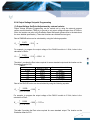
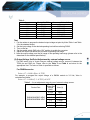
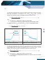
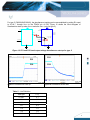
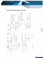
DNS SIP Series Evaluation Procedure (DEP-008 A) The Delphi DNS Series of SIP type POL converters The DNS, 2.4~5.5V or 10~14V input, programmable output, non-isolated point of load DC/DC converters, are the latest offering from one of the world’s largest power supply manufacturers ― Delta Electronics, Inc. The DNS converters have flexible and programmable tracking and sequencing features to enable a variety of startup voltages as well as sequencing and tracking between power modules. With creative design technology and optimization of component placement, these converters possess outstanding electrical and thermal performance, as well as extremely high reliability under highly stressful operating conditions. All models possess a myriad of standard protection features. 1.0 Purpose This document guides the user in performing electronic measurements on a DNS POL (point of load) DC/DC converter using the Delta Evaluation Board. 2.0 Relevant Documentation This document guides the user through the evaluation procedures to qualify a POL module. The data shown in this Evaluation Procedure is for the SIP Package Type POL evaluation board. Please refer to the appropriate technical data sheet for detailed performance and technical information for the specific POL units. Evaluation Procedure EP_DNS_SIP_08052004 The documentation and background information listed below is relevant to this evaluation procedure: 2.1 Appropriate date sheet for the DNS Series unit under evaluation. 2.2 Power Module Evaluation Board Schematic. 2.3 Power Module Evaluation Board Layout. 2.4 General Test and Safety Procedures. 1 Delta Electronics, Inc. 3.0 Equipment Required 3.1 A DC Power Supply 0 - 20 V @ 0 - 20A (Agilent 6574A 0 -60V/0 - 35A or equivalent). 3.2 An oscilloscope (Tektronix TDS 3034 or equivalent) 4 Channel 300 MHz, equipped with a x1 scope probe, a x10 scope probe, and two BNC cables (length less than 20 inches/500mm) 3.3 Digital multi-meters, one with 20A range and ideally all with 4 1/2 digit resolution (DVM1, DVM2 and DVM3) (Zentech 2041 or equivalent). 3.4 An electronic load (Chroma 63030 or equivalent), 300W approximate rating, or a suitable resistive load. 3.5 A DC power supply (GW GPC-3060D). 4.0 Equipment Set-Up and Description Refer to the Power Module Evaluation Board Layout (See page 20) for reference designators cited in this document and Figure 1. Set-up Diagram. Figure 1. Set-up Diagram 2 4.1 Connect one lead from the “+” lead of the DC source (See Item 3.1) to the “20A” terminal of the first multi-meter DVM1 (See Item 3.3). Then connect one lead from the “Common” of the DVM1 to the “Vin” pin of the Evaluation Board. DVM1 is used to measure the input current. 4.2 Connect one wire from the “-” lead of the DC source (See Item 3.1) to the “GND“ pin of the Evaluation Board. Note: Use stranded leads at least equivalent to 14 AWG for all connections in sections 4.1 and 4.2. The leads should be twisted to reduce noise coupling. 4.3 Connect the plus “+” and minus “-“ connection leads from a second multi-meter (See Item 3.3) to the “SVin” and “SGND” pins on the Evaluation Board. This multi-meter is designated DVM2. DVM2 is used to measure the input voltage. 4.4 Connect the plus “+” and minus “-“ connection leads from the third multi-meter (See Item 3.3) to the “SVOUT” and “SGND” Pin on the Evaluation Board. The multi-meter is designated DVM3. DVM3 is used to measure the output voltage. 4.5 Connect a BNC cable (length less than 20 inches/500mm) from BNC1 of the Evaluation Board to Channel 1 of the oscilloscope (See Item 3.2). This cable is used to measure the input voltage (between SVIN and SGND). 4.6 Connect a BNC cable (length less than 20 inches/500mm) from BNC2 of the Evaluation Board to Channel 2 of the oscilloscope (See Item 3.2). This cable is used to measure the output voltage (between SVOUT and SGND). 4.7 Connect the positive and negative power leads of the electronic load (ensuring correct polarity), or an appropriate resistive load to the Evaluation Board output terminal pin (“Vout” for positive power lead and “SGND” for the negative power lead). 4.8 Connect one lead from the “+” lead of the DC source (See Item 3.5) to the “12Vcc” on the Evaluation Board. Then connect one lead from the “-” of the DC source (See Item 3.5) to the “12VGND” on the Evaluation Board. 5.0 Thermal Management of the Converter It is imperative that sufficient airflow needs to be provided to the converter at all times during all portions of testing. Please refer to the applicable data sheet for the proper cooling and derating necessary conditions to obtain accurate results when testing the converter. 3 6.0 Tests Performed The following tests are performed at room temperature (+25 ℃). 6.1 Input Characteristics Input Voltage Range. Under-Voltage Lockout. No Load Input Current. 6.2 Output Characteristics Line Regulation. Load Regulation. Output Regulation. Output Voltage Set-point Programming Output Voltage Margining Output Voltage Tracking 6.3 Dynamic Characteristics Maximum Output Voltage Deviation (due to step change in load). Turn on Response time. 6.4 Thermal Characteristic Efficiency 7.0 Test Set-Up 7.1 Initial Set-Up 1) Examine the part number of the power module to determine that the correct module is being evaluated. Note: DNS04S0A0S06P A would denote the SMT package, while DNS04S0A0R06P A would denote the SIP package. This Evaluation Board is for use with SIP package. 2) Set the multi-meter DVM1 to the DC current 20A range. Set multi-meters DVM2 and DVM3 to DC voltage, auto ranging. 3) Electronic Load Turn on the Electronic Load at CR mode (or resistive load) and adjust the current level. The maximum rated output current is 6A. Ensure the output load does not exceed the recommended maximum current. 4) SW1 is used for on/off Transient function test. Turn SW1 to the OFF position if this function is not being used. Turn SW1 to the ON position if the Transient function test is required. 4 5) SW2 is used to enable or disable the converter. For positive logic module, When SW2 is put in the ON position, the converter is ON and when SW2 is put in the OFF position, the converter is OFF. For negative logic module, When SW2 is put in the OFF position, the converter is ON, and when SW2 is put in the ON position, the converter is OFF. 6) SW3 is used for the Output Voltage Set-Point Adjustment Range. By an external voltage source: If the converter requires a trim up, set the SW3_1 to ON position. If the converter requires a trim down, set the SW3_2 to ON position. By an external resistor: If the converter requires a trim up to Vo,set, set the SW3_8 to ON position. If the converter requires a margin trim down, set the SW3_3 to ON position. If the converter requires a margin trim up, set the SW3_4 to ON position. Please refer to the SW3 Function table. SW3 Function table Subdivide switch No. SW3_1 SW3_2 SW3_3 SW3_4 SW3_8 Function Voltage trim up Voltage trim down Resistor margin trim down Resistor margin trim up Resistor trim up Note: 1. The subdivide switch of SW3_1~4 must not be ON at the same time. 2. For the SW3_5~7 use at NPA series, must set to OFF position. 7.2 Initial Power Up 1) Turn the power supply ON, set the current limit on DC source (refer to specification of either converter) and increase the input voltage (use DVM2 to monitor the input voltage) until it reaches the desired value. 2) Set the switch SW2 to power module ON. 3) The converter is now operating, which can be verified by observing the DVM3 (appropriate value for the nominal output voltage) and channel 2 of the oscilloscope (appropriate value for the nominal output voltage). 4) Set the switch SW2 to power module OFF. 5 8.0 Tests and Evaluation 8.1 Input Characteristics 8.1.1 Input Voltage Range and Under-Voltage Lockout The DNS04xx Series of DC/DC converters will operate at full load from 2.4Vin to 5.5Vin for 5Vin (nominal) types. The DNS12xx Series DC/DC converters will operate at full load from 10Vin to 14Vin for 12Vin (nominal) types. The converters feature input under-voltage protection, which will not allow the converter to start up unless the input voltage exceeds the turn-on voltage threshold. Test 1) Turn on the fan. 2) Set the input voltage to the desired operating point while monitoring DVM2. 3) Set the switch SW2 to the “ON or OFF” position to enable the converter. (See Item 7.1.5) 4) Test the input under voltage function while observing DVM2, DVM3 and channel 1 of the oscilloscope. Increase the input voltage until the output of the converter reaches the appropriate value. This will occur between 2.05 and 2.25 volts for 5Vin nominal and between 9.0 to 10 volts for 12Vin nominal. Please refer to the appropriate converter data sheet for the detailed specification. 8.1.2 No Load Input Current Test 1) 2) 3) 4) 5) 6) Turn on the fan. Set the input voltage to the desired operating point while monitoring DVM2. Set the switch SW2 to the converter ON. Remove/disable the output electronic load or resistive load. Note the input current from DVM1. The result is the No-Load Input current of the DC/DC converter. The No-Load Input Current will be around 50 to 150 mA depending on the model under evaluation. (Please refer to the data sheet for the detailed specification). 6 8.2 Output Characteristics 8.2.1 Line Regulation Line Regulation Deviation is defined as the change in output voltage caused by varying the input voltage over a specified range while the output load and temperature remain constant. Test 1) 2) 3) 4) Turn on the fan. Set the output power to the desired operating point. Set the switch SW2 to the converter ON. Adjust the input voltage across the converter’s input range (refer to specified range) while monitoring DVM2. 5) Note the maximum +/- deviation of the output voltage over the full range of the input operating voltage (please refer to the data sheet for the detailed specification). 8.2.2 Load Regulation Load Regulation Deviation is defined as the change in output voltage caused by varying the output load current over the specified range (no load to full load) while the input voltage and temperature remain constant. Test 1) 2) 3) 4) 5) Turn on the fan. Set the input voltage to the desired operating level while monitoring DVM2. Set the switch SW2 to the converter ON. Adjust the output load across the converter’s operating load range. Note the maximum +/- deviation of the output voltage over the full range of the operating load range (please refer to the data sheet for the detailed specification). 8.2.3 Output Ripple Output Ripple is defined as the periodic AC component on the DC/DC converter’s output voltage. The output ripple is measured in terms of peak to peak and RMS values, both done with a specific bandwidth. Test 1) Turn on the fan. 2) Set the switch SW2 to the converter ON. 3) Adjust the input voltage while monitoring DVM2 and set the output load to the full rated load current. 4) Adjust channel 2 on the oscilloscope to be AC coupled at 4µS/Div and at 10mV/Div using the 20 MHz bandwidth-limit option on the scope. 5) The output ripple of the DC/DC converter is measured at full load operating power. 7 8.2.4 Output Voltage Set-point Programming (1) Output Voltage Set-Point Adjustment by external resistor Output Voltage Set-point Programming can be carried out by using the external program resistor connect between TRIM pin to ground to set output voltage set-point from 0.75Vdc to 5Vdc, the location can refer to the Evaluation Board Schematic (please refer to the data sheet for more detailed specification). These test functions are divided into two types, Rset of DNS04R series can be calculated by using the following equation: 21070 R set = − 5110 Vo − 0.7525 Ω For example, to program the output voltage of the DNS04 module to 1.8Vdc, below is the calculation of Rtrim: 21070 − 5110 = 15004 Ω Rset = 1.8 − 0.7525 The table 1 provides the Rset value required for some standard output and the location on the Evaluation board is R33. Table 1. Recommend Value, R//R Vo,set Rset (k Ω ) R33 0.7525 Open Open 1.2 41.973 44.2k//825k 1.5 23.077 23.7k//825k 1.8 15.004 15.4k//590k 2.5 6.947 7.15k//243k 3.3 3.160 3.16k//Open Rset of the DNS12R series can be calculated by using the following equation: 10500 Rset = − 1000 Vo − 0.7525 Ω For example, to program the output voltage of the DNS12 module to 3.3Vdc, below is the calculation of Rset: 10500 R set = − 1000 = 3122 Ω 3.3 − 0.7525 The table 2 provides the Rset value required for some standard output. The location on the Evaluation board is R33. 8 Table 2. Vo,set 0.7525 1.2 1.5 1.8 2.5 3.3 5.0 Rset (k Ω ) R33 Open 22.464 13.047 9.024 5.009 3.122 1.472 Recommend Value, R//R Open 23.7k//432k 14.0k//191k 9.53k//169k 5.23k//118k 3.16k//261k 1.5k//78.7k Test 1. Put the resistor to program the desired output voltage set point by follow Table 1 and Table 2 for the standard output. 2. Set the input voltage to the desired operating level while monitoring DVM2. 3. Turn on the fan. 4. Set the enable switch SW2 to the “ON” position to enable the converter. 5. Adjust the output load across the converter’s operating load range. 6. Note the output voltage over the full range of the operating load range (please refer to the data sheet for the detailed specification). (2) Output Voltage Set-Point Adjustment by external voltage source For DNS series, trim to Vo,set using an external voltage source, connect it between the TRIM pin and GND pin. Please refer to the Table 3 and Table 4 as below for the appropriate Vout. The value of Vtrim is specified as follows: For DNS04xx series Vtrim = 0.7 − 0.1698 × (Vout − 0.7525) For example, to program the output voltage of a DNS04 module to 3.3 Vdc, Vtrim is calculated as follows: Vtrim = 0.7 − 0.1698 × (3.3 − 0.7525) = 0.267V Table 3. : Vo,set adjustment range by use of external voltage source. Normal Output Set Product Part Vrim (V) Voltage (Vdc) 0.7525 Open DNS04S0A0R06P A/B/C DNS04S0A0R06N A/B/C 1.2 0.6240 1.5 0.5730 1.8 0.5220 2.5 0.4030 3.3 0.2670 9 For DNS12xx series Vtrim = 0.7 − 0.0667 × (Vout − 0.7525) V For example, to program the output voltage of a DNS12 module to 3.3 Vdc, Vtrim is calculated as follows Vtrim = 0.7 − 0.0667 × (3.3 − 0.7525) = 0.53 V Table 4. : Vo,set adjustment range by use of external voltage source. Normal Output Set Vrim (V) Product Part Voltage (Vdc) 0.7525 Open DNS12S0A0S06P A/B/C DNS12S0A0S06N A/B/C 1.2 0.670 1.5 0.650 1.8 0.630 2.5 0.583 3.3 0.530 5.0 0.4167 8.2.5 Voltage Margining Output voltage margining can be carry out by connecting a resistor from the Trim pin to ground pin for trim up and connecting a resistor from Trim pin to Output pin for Trim down. The Rmarginup is for trim up and Rmargin-down is for trim down. (Please refer to the data sheet and Evaluation Board Schematic for the detailed information). A software tool for voltage margining calculation is available to ask for. The values of Rmarginup and Rmargin-down for a specific output voltage and margin percentage can then be figured out. Please consult your local Delta Field Application Engineer or sales persons for additional information. Test 1) Connect a trim resistor for a desired voltage value (Please refer to Table 1 and Table 2). 2) Turn on the fan. 3) Adjust the input voltage while monitoring DVM2 and with output load set to the desired operating point. 4) Set the enable switch SW2 to the “ON” position to enable converter. 5) Use SW3 (refer to Item 7.1_6) for Trim setup. 6) Note the voltage by observing DVM3. 7) Test the Load Regulation (refer to Item 8.2.2). 10 8.2.6 Voltage Tracking The DNS family was designed for applications that have output voltage tracking requirements during power-up and power-down. The devices have a TRACK pin to implement three types of tracking method: sequential, ratio-metric and simultaneous. TRACK simplifies the task of supply voltage tracking in a power system by enabling modules to track each other, or any external voltage, during power-up and power-down. By connecting multiple modules together, customers can get multiple modules to track their output voltages to the voltage applied on the TRACK pin. Detailed Description Sequential Implementation Sequential start-up is implemented by connecting the power good signal (PWRGD pin) of PS1 to the TRACK pin of PS2 with a resistor–capacitor (RC) circuit. The waveforms of power up and down are in Figures 4 and 5. In Figure 4, the 5V PS1 supply ramps up first. When supply reaches its final 5V steady state value, the open collector output of the PWRGD pin releases to the TRACK pin and the PS2 output voltage rises at the rate of the RC time constant. In Figure 5, the PWRGD pin pull low by PS1 ENABLE off or the PS1 output voltage is below 90% of the desired regulated voltage, and then the TRACK pin is pulled low and the PS2 power down. Figure 3 shows the circuit diagram of sequential start-up when VoPS2 tracks the PWRGD of PS1. PS1 PS2 Vin Vin VoPS2 VoPS1 PWRGD TRACK R ENABLE ENABLE C Figure 3. PS1 and PS2 track output voltage Sequential start-up 11 PS1 PS1 PS2 PS2 Figure 4: Sequential Power up Figure 5: Sequential Power down Ratio-Metric Implementation Ratio–metric is implemented by the selection of the resistor values of the voltage divider on the TRACK pin. Resistors R1 and R2, in Figure 6 determine the tracking method that is implemented. To simplify the tracking design, set initial value of R2 equal to 20KΩ at internal circuit and set resistor R1 for different tracking method. Figure 6 shows the circuit diagram of Ratio-Metric start-up when VoPS2 tracks the VoPS1. PS2 PS1 Vin Vin VoPS2 VoPS1 R1 TRACK ENABLE ENABLE To Tracking circuit R2 20K Figure 6. PS1 and PS2 track output voltage Ratio-Metric start-up 12 For Ratio-Metric applications that need the PS1 and PS2 outputs arrive regulation set point at same time, use equation 1 to calculate R1, set △ V=Voset,PS1–Voset,PS2 and △ V will be negative. The waveforms of power up and down are showed in Figures 7 and 8. R1 = [(Vo set , PS 2 + ∆V ) − Vref ] Vref * 20 K Ω ------------------------------------------------------(1) Note: 1. Vref =0.4×Voset,PS2 , please refer to Table 5 for Vref set value. 2. △V is the maximum difference of voltage between PS1 and PS2 supply voltage. For example, the PS1 Voset,PS1=5V, the PS2 Voset,PS2=3.3V, R1 is calculated as follows: R1 = [(3.3 + 1.7) − 1.32] * 20 K = 55.75 K Ω 1.32 +△V=1.7V PS1=5V PS1 PS2=3.3V PS2 Figure 7. Ratio–metric tracking Power up Figure 8. Ratio–metric tracking Power down For Ratio-Metric applications that need the PS2 supply voltage rises first at power up and falls second at power down, use equation 2 to calculate R1, set △V≦0.4×Voset,PS2 and △V will be negative. The waveforms of power up and down are showed in Figures 9 and 10. R1 = [(Vo set , ps 2 − ∆V ) − Vref ] Vref * 20 K -----------------------------------------------------------------(2) Note: 1. Vref =0.4×Voset,PS2 , please refer to Table 5 for Vref set value. 2. △V is defined as the voltage difference between VoPS1 and VoPS2 when VoPS2 reaches its rated voltage. 13 For example, the PS1 Voset,PS1=5V, the PS2 Voset,PS2=3.3V, R1 is calculated as follows: R1 = [(3.3 − 1.3) − 1.32] * 20 K = 10.303K Ω 1.32 PS1=5V PS1 PS2=3.3V PS2 -△V=1.3V Figure 9. Ratio–metric tracking Power up Figure 10. Ratio–metric tracking Power down Simultaneous Implementation Similar to the ratio-metric implementation, simultaneous tracking is implemented by using a voltage divider on the TRACK pin. The objective is to minimize the voltage difference between the power supply outputs during power up and down. The waveforms of power up and down are showed in Figures 13 and 14. For type A (DNXXX0A0XXXX A), the simultaneous tracking can be accomplished by connecting VoPS1 to the TRACK pin of PS2. Figure 11 shows the circuit diagram of voltage Simultaneous start-up when VoPS2 tracks VoPS1 (only for type A). PS2 PS1 Vin Vin VoPS2 VoPS1 TRACK ENABLE ENABLE Figure 11. PS1 and PS2 track output voltage Simultaneous start-up for type A 14 For type C (DNXXX0A0XXXX C), the simultaneous tracking can be accomplished by putting R1 equal to 30.1K Ω through VoPS1 to the TRACK pin of PS2. Figure 12 shows the circuit diagram of Simultaneous start-up when VoPS2 tracks the VoPS1 (only for type C). PS2 PS1 Vin Vin VoPS2 VoPS1 30.1K R1 TRACK ENABLE ENABLE R2 To Tracking circuit 20K Figure 12. PS1 and PS2 track output voltage Simultaneous start-up for type C PS1 PS1 PS2 PS2 Figure 13. Simultaneous Power up Figure 14. Simultaneous Power down Table 5. : Vref Definition Voset,ps2 Vref 0.7525 0.3 1.2 0.48 1.5 0.6 1.8 0.72 2.5 1.0 3.3 1.32 5.0 2.0 15 Notes on the use of Track function: 1. For proper voltage tracking, first, The ENABLE On/Off pin of the PS2 module is left unconnected (or tied to GND for negative logic modules or tied to VIN for positive logic modules), so that the modules are ON by default and second applied input voltage to the PS1 and PS2. The TRACK pin is held at ground potential for duration of input voltage reaches its minimum input voltage (VIN,min) and then held for at least 10mS thereafter. This brief period gives the modules time to complete their internal soft-start initialization. 2. The PS2 output will not follow the PS1 voltage until the PS2 has completed its soft-start time. After this time, PS2 is capable of both sinking and sourcing current when following the voltage at the TRACK pin. 3. Notice that power down by removing the input voltage may not provide proper power tracking below under voltage lockout limit where the both integrated switches are off. So, using the ENABLE On/Off signal of PS1 for power down is the preferred option for power tracking. 4. The TRACK pin absolute maximum voltage cannot over the Vin. 5. For type A: When Tracking is unused, put R1 equal to 1KΩ and connect TRACK pin to +Vcc For type C: When Tracking is unused, put R1 equal to 30.1KΩ and connect TRACK pin to +Vcc Test 1) Put R56 to take the place of R1 on the POL evaluation board and use the value from above equation for different tracking purpose. 2) Use channel 1 and channel 2 measures the output voltage of PS1 and PS2. 3) For turn on, disable remote On/Off of the PS1, enable remote On/off of the PS2, and supply input voltage to PS1 and PS2. 4) For the power on, enable switch on of PS1. In the meantime, to track power up by scope trigger function. 5) For the power down, enable switch off of PS1 to track power down. 6) Illustration of tacking features can be found in the section of Detailed Description. 8.3 Dynamic Characteristics 8.3.1 Output Voltage Deviation Output Voltage Deviation is defined as the response of the converter to a sudden step change in the output load current. The output voltage deviation is characterized by two parameters: Maximum Output Voltage Deviation and Response Time (please refer to the data sheet for the detailed specification). The value of dynamic resistance for a defined step current is defined as: Rdynamic = Vout 0.5 * Imax 16 Test 1) 2) 3) 4) Turn on the fan. Adjust the input voltage to the desired operating point. Set the electronic or resistive load at 50% of maximum load. Change channel 1 to scope probe and measure across the Rdynamic . 5) Set the switch SW2 to the converter ON. 6) Set channel 2 on the oscilloscope to be AC coupled and to 50mV/Div and for 5mS/Div. Set the trigger to auto and adjust the trigger point at a negative going pulse for step load change from 50% to 100% of Io or adjust the trigger point at positive going pulse for step load change from 100% to 50% (Please refer to data sheet for the detailed information.) 7) Measure the Peak-to-Peak deviation and capture the waveform as required. 8.3.2 Turn-On Response Time. Turn-On Response Time is defined as the time it takes for the output to rise to within 90% of its final value from the time when the converter is enabled. The rise time is deliberately made slower to reduce the inrush current and to eliminate any overshoot in the output voltage. These test functions have two categories. 1.) Turn on the module by using the External switch to control input voltage. 2.) Turn on module by using the Enable on/off. Test (Turn on the module by using the external switch) 1) Turn on the fan. 2) Turn on the input power supply and set it to the desired operating point. 3) Set channel 1 on the oscilloscope to be DC coupled and to the appropriate range for the input voltage. 4) Connect a coaxial cable from channel 1 to BNC1 on the Evaluation Board. 5) Set channel 2 on the oscilloscope to be DC coupled and to the appropriate range for the output voltage. 6) Connect a coaxial cable from channel 2 to BNC2 on the Evaluation Board. 7) Set the Time base to 2mS/Div 8) Set the Trigger for a one-time event and set the Trigger level at approximately 2V (rising) or suitable trigger point (referring to data sheet) on channel 2. 9) Enable the external on/off switch to supply power and use the cursor V Bars to measure the delay time, and then record the waveform on the oscilloscope. Test (Turn on the module by using the Enable on/off) 1. Turn on the fan. 2. Turn on the input power supply and set it to the desired operating point. 3. Set channel 1 on the oscilloscope to be DC coupled and to 1V/division. (Please also refer to data sheet for the detailed information). 4. Connect a scope probe from channel 1 between the on/off control pin and reference ground (SGND) on the Evaluation Board. 17 5. Set channel 2 on the oscilloscope to be DC coupled and to the appropriate range for the output voltage. 6. Connect a coaxial cable from channel 2 to BNC2 on the Evaluation Board. 7. Set the Time base to 2mS/Div 8. Set the Trigger for a one-time event and set the Trigger level at approximately 2V (rising) or suitable trigger point (referring to data sheet) on channel 2. 9. Enable the on/off switch to turn on and use the cursor V Bars to measure the delay time, and then record the waveform on the oscilloscope. 8.4. Thermal Characteristic 8.4.1 Efficiency Efficiency is the ratio of total output power to the input power. It is typically measured at full load and nominal input voltage. Test 1) 2) 3) 4) 5) 6) 7) Turn on the fan. Set the enable switch SW2 to the converter ON. Adjust the input voltage to the desired operating point. Set the electronic or resistive Load to the desired operating point. Read and note the output voltage (DVM3) and input voltage (DVM2). Read and note the input and output currents from the DVM1 and the electronic load. Use the following formulas to calculate the efficiency: Efficiency= (Pout/Pin) × 100(%) Pin = Iin × Vin Pout = Iout × Vout The following graph shows the efficiency curves of the DNS04S0A0R06P A module when measuring at different operating points. 100 EFFICIENCY(%) 90 80 70 60 3V 50 5V 40 5.5V 30 1 2 3 LOAD (A) 4 5 6 18 Appendix A- Evaluation Board Schematic 19 Appendix B - Evaluation Board Layout (Top View) Appendix C - Evaluation Board Layout (Bottom View) CONTACT DATA: www.deltaww.com USA: Telephone: East Coast: (888) 335 8201 West Coast: (888) 335 8208 Fax: (978) 656 3964 Email: [email protected] Europe: Telephone: France: +33 1 6485 1212 Germany: +49 89 370 62 897 UK: +44 777 195 6299 Fax: +33 1 6485 1212 Email: [email protected] Asia: Telephone: +886 3 4526107 x6220 Fax: +886 3 4513485 Email: [email protected] Warranty Delta offers a two (2) year limited warranty. Complete warranty information is listed on our web site or is available upon request from Delta. Information furnished by Delta is believed to be accurate and reliable. However, no responsibility is assumed by Delta for its use, nor for any infringements of patents or other rights of third parties, which may result from its use. No license is granted by implication or otherwise under any patent or patent rights of Delta. Delta reserves the right to revise these specifications at any time, without notice. 20