1
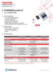
FEATURES High efficiency: 92.5% @ 12Vin, 3.3V/50A out Size: 61.0x31.8x10.2mm y (2.40”×1.25”×0.40”) Voltage and resistor-based trim No minimum load required Output voltage programmable from 0.9Vdc to 3.63Vdc via external resistors Fixed frequency operation Single-in line package (SIP) Input UVLO, output OCP, OTP, SCP Remote ON/OFF (Positive) Power good output signal (open collector) Output voltage sense ISO 9001, TL 9000, ISO 14001, QS9000, OHSAS18001 certified manufacturing facility UL/cUL 60950-1 (US & Canada), TUV (EN60950-1) - pending Delphi ND Series Non-Isolated Point of Load DC/DC Power Modules: 12Vin, 0.9V~3.63Vout, 50Aout The Delphi ND Series, 12V input, single output, non-isolated point of load (POL) DC/DC converters are the latest offering from a world leader in power systems technology and manufacturing — Delta Electronics, Inc. The ND/NE product family is the second generation, non-isolated point-of-load DC/DC power modules for the DataCom / Networking / IT Applications and it will help to cut the module size by 35% to 50% compared to the first generation NC series POL modules. The ND/NE product family provides 6A to 60A of output current in a vertically or horizontally mounted through-hole package and the output can be resistor trimmed from 0.9Vdc to 3.63Vdc. It provides a very cost effective, high efficiency, and high density point of load solution. With creative design technology and optimization of component placement, these converters possess outstanding electrical and thermal performance, as well as extremely high reliability under highly stressful operating conditions. PRELIMINARY DATASHEET DS_ND12S50A_07172008 OPTION Negative on/off logic Current sharing APPLICATIONS DataCom Distributed power architectures Servers and workstations LAN / WAN applications Data processing applications TECHNICAL SPECIFICATIONS (Ambient Temperature=25°C, minimum airflow=200LFM, nominal Vin=12Vdc unless otherwise specified.) PARAMETER NOTES and CONDITIONS ND12S0A0V50 (Standard) Min. ABSOLUTE MAXIMUM RATINGS Input Voltage Operating Temperature Storage Temperature Input/Output Isolation Voltage INPUT CHARACTERISTICS Operating Input Voltage Input Under-Voltage Lockout Turn-On Voltage Threshold Turn-Off Voltage Threshold Lockout Hysteresis Voltage Maximum Input Current No-Load Input Current Off Converter Input Current Inrush Transient Input Reflected-Ripple Current Input Ripple Rejection OUTPUT CHARACTERISTICS Output Voltage Adjustment Range Output Voltage Set Point Output Voltage Regulation Over Load Over Line Total output range Output Voltage Ripple and Noise Peak-to-Peak RMS Output Current Range Output Voltage Over-shoot at Start-up Output Voltage Under-shoot at Power-Off Output DC Current-Limit Inception DYNAMIC CHARACTERISTICS Output Dynamic Load Response Positive Step Change in Output Current Negative Step Change in Output Current Settling Time Turn-On Transient Start-Up Time, from On/Off Control Start-Up Time, from input power Minimum Output Capacitance Maximum Output Startup Capacive Load Minimum Input Capacitance EFFICIENCY Vo=0.9V Vo=1.2V Vo=1.5V Vo=1.8V Vo=2.5V Vo=3.3V Vo=3.63V FEATURE CHARACTERISTICS Switching Frequency ON/OFF Control Logic High Logic Low Remote Sense Range GENERAL SPECIFICATIONS Calculated MTBF Weight Over-Temperature Shutdown DS_ND12S10A_07172008 Refer to Figure 32 for the measuring point Typ. -0.3 0 -40 Non-isolated Max. Units 13.8 124 125 Vdc °C °C V NA 10.2 12.0 13.8 V 8.5 7.1 9.0 7.6 1.4 9.5 8.1 V V V A mA mA A2S mA dB 100% Load, 10.2Vin, 3.3Vout Vin=12V, Vout=3.3V Remote OFF Vin=10.2~13.8V, Io=Min to Max Load Refer to Figure 31. 120Hz With a 1.0% trim resistor Io=Io_min to Io_max Vin=Vin_min to Vin_max Over load, line, temperature regulation and set point 5Hz to 20MHz bandwidth Full Load, 1uF ceramic, 10uF Tan cap and 4*680uF OSCON Full Load, 1uF ceramic, 10uF Tan cap and 4*680uF OSCON 15 20 60 0.9 -2 3.63 +2 V % -1 -0.2 -3 +1 +0.2 +3 % % % 50 15 50 2 100 200 mV mV A % mV %Iomax 25 5 0 Vin=12V, Turn ON Vin=12V, Turn OFF Hiccup mode 110 12Vin, 1uF ceramic, 10uF Tan cap and 4*680uF OSCON 25A to 37.5A, 10A/uS 37.5A to 25A, 10A/uS Settling to be within regulation band (to 10% Vo deviation) From Enable high to 90% of Vo From Vin=12V to 90% of Vo Ex: One OSCON 6.3V/680uF (ESR=13mΩ max) Full Load (ESR≧1mΩ) 24 250 30 1.00 75 75 50 mV mV µs 10 10 680 3000 0 ms ms µF µF µF Vin=12V, Io=50A Vin=12V, Io=50A Vin=12V, Io=50A Vin=12V, Io=50A Vin=12V, Io=50A Vin=12V, Io=50A Vin=12V, Io=50A 81 84.5 87 88.5 91 92.5 92.8 % % % % % % % Fixed Positive logic (internally pulled high) Module On (or leave the pin open) Module Off 300 KHz Telcordia SR-332 Issue1 Method1 Case3 at 50°C Refer to Figure 32 for the measuring point 2.4 -0.2 Vinmax 0.8 0.5 TBD 34.2 134 V V V Mhours grams °C 2 95 95 90 90 EFFICIENCY (%) EFFICIENCY (%) ELECTRICAL CHARACTERISTICS CURVES 85 80 75 70 5.01 10.2 10 15 20 25 12.0 30 35 13.8 40 45 85 80 75 70 5.01 50 10.2 10 OUTPUT CURRENT (A) 90 95 EFFICIENCY (%) EFFICIENCY (%) 100 85 80 70 5.01 10 15 20 25 12.0 30 35 13.8 40 45 75 EFFICIENCY (%) EFFICIENCY (%) 95 90 85 80 20 25 12.0 30 35 13.8 40 OUTPUT CURRENT (A) Figure 5: Converter efficiency vs. output current (2.5V output voltage) DS_ND12S10A_07172008 50 10.2 15 20 25 12.0 30 35 13.8 40 45 50 Figure 4: Converter efficiency vs. output current (1.8V output voltage) 95 15 45 OUTPUT CURRENT (A) 100 10 40 80 100 70 5.01 35 85 70 5.01 10 50 Figure 3: Converter efficiency vs. output current (1.5V output voltage) 10.2 30 90 OUTPUT CURRENT (A) 75 25 Figure 2: Converter efficiency vs. output current (1.2V output voltage) 95 10.2 20 13.8 OUTPUT CURRENT (A) Figure 1: Converter efficiency vs. output current (0.9V output voltage) 75 15 12.0 45 50 90 85 80 75 70 5.01 10 10.2 15 20 25 30 12.0 35 13.8 40 45 50 OUTPUT CURRENT (A) Figure 6: Converter efficiency vs. output current (3.3V output voltage) 3 ELECTRICAL CHARACTERISTICS CURVES (CON.) Figure 7: Output ripple & noise at 12Vin, 0.9V/50A out Figure 8: Output ripple & noise at 12Vin, 1.2V/50A out Figure 9: Output ripple & noise at 12Vin, 1.5V/50A out Figure 10: Output ripple & noise at 12Vin, 1.8V/50A out Figure 11: Output ripple & noise at 12Vin, 2.5V/50A out Figure 12: Output ripple & noise at 12Vin, 3.3V/50A out DS_ND12S10A_07172008 4 ELECTRICAL CHARACTERISTICS CURVES (CON.) Figure 13: Turn on delay time at 12Vin, 0.9V/50A out Ch1: Vout Ch4: Vin Figure 14: Turn on delay time Remote On/Off, 0.9V/50A out Ch1: Vout Ch4: Enable Figure 15: Turn on delay time at 12Vin, 3.3V/50A out Ch1: Vout Ch4: Vin Figure 16: Turn on delay time at Remote On/Off, 3.3V/50A out Ch1: Vout Ch4: Enable Figure 17: Typical transient response to step load change at 10A/μS from 50%to 75% and 75% to 50 of Io, max at 12Vin, 0.9V out Figure 18: Typical transient response to step load change at 10A/μS from 50%to 75% and 75% to 50 of Io, max at 12Vin, 1.2V out DS_ND12S10A_07172008 5 Figure 19: Typical transient response to step load change at 10A/μS from 50%to 75% and 75% to 50 of Io, max at 12Vin, 1.5V out Figure 20: Typical transient response to step load change at 10A/μS from 50%to 75% and 75% to 50 of Io, max at 12Vin, 1.8V out Figure 21: Typical transient response to step load change at 10A/μS from 50%to 75% and 75% to 50 of Io, max at 12Vin, 2.5V out Figure 22: Typical transient response to step load change at 10A/μS from 50%to 75% and 75% to 50 of Io, max at 12Vin, 3.3V out DS_ND12S10A_07172008 6 DESIGN CONSIDERATIONS FEATURES DESCRIPTIONS The ND 50A uses two phase and voltage mode controlled buck topology. The output can be trimmed in the range of 0.9Vdc to 3.63Vdc with a resistor from Trim pin to Ground. A remote sense function is provided and it is able to compensate for a drop from the output of converter to point of load. ENABLE (On/Off) The converter can be turned ON/OFF by remote control. Positive on/off (ENABLE pin) logic implies that the converter DC output is enabled when the signal is driven high (greater than 2.4V) or floating and disabled when the signal is driven low (below 0.8V). Negative on/off logic is optional. The converter provides an open collector Power Good signal. The power good signal is pulled low when output is not within ±10% of Vout or Enable is OFF. The converter can protect itself by entering hiccup mode against over current and short circuit condition. The converter has an over temperature protection which can protect itself by shutting down for an over temperature event. There is a thermal hysteresis of typically 20°C The ENABLE (on/off) input allows external circuitry to put the ND converter into a low power dissipation (sleep) mode. Positive ENABLE is available as standard. Positive ENABLE units of the ND series are turned on if the ENABLE pin is high or floating. Pulling the pin low will turn off the unit. With the active high function, the output is guaranteed to turn on if the ENABLE pin is driven above 2.4V. The output will turn off if the ENABLE pin voltage is pulled below 0.8V. The ENABLE input can be driven in a variety of ways as shown in Figures 23 and 24. If the ENABLE signal comes from the primary side of the circuit, the ENABLE can be driven through either a bipolar signal transistor (Figure 23). If the enable signal comes from the secondary side, then an opto-coupler or other isolation devices must be used to bring the signal across the voltage isolation (please see Figure 24). Safety Considerations It is recommended that the user to provide a fuse with TBD in the input line for safety. The output voltage set-point and the output current in the application could define the amperage rating of the fuse. Figure 23: Enable Input drive circuit for ND series Figure 24: Enable input drive circuit example with isolation. DS_ND12S10A_07172008 7 FEATURES DESCRIPTIONS (CON.) Input Under-Voltage Lockout The input under-voltage lockout prevents the converter from being damaged while operating when the input voltage is too low. The lockout occurs between 7.6V to 9.0V. Over-Current and Short-Circuit Protection The ND series modules have non-latching over-current and short-circuit protection circuitry. When over current condition occurs, the module goes into the non-latching hiccup mode. When the over-current condition is removed, the module will resume normal operation. Over Temperature Protection (OTP) To provide additional over-temperature protection in a fault condition, the unit is equipped with a non-latching thermal shutdown circuit. The shutdown circuit engages when the temperature of monitored component exceeds approximately 125°C. The unit will cycle on and off while the fault condition exists. The unit will recover from shutdown when the cause of the over temperature condition is removed Output Voltage Programming The output voltage of the ND series is trimmable by connecting an external resistor between the trim pin and output ground as shown Figure 26 and the typical trim resistor values are shown in Figure 27. An over current condition is detected by measuring the voltage drop across the MOSFETs. The voltage drop across the MOSFET is also a function of the MOSFET’s Rds(on). Rds(on) is affected by temperature, therefore ambient temperature will affect the current limit inception point. The detection of the Rds(on) of MOSFETs also acts as an over temperature protection since high temperature will cause the Rds(on) of the MOSFETs to increase, eventually triggering over-current protection. Remote sense The ND50 provide Vo remote sensing to achieve proper regulation at the load points and reduce effects of distribution losses on output line. In the event of an open remote sense line, the module shall maintain local sense regulation through an internal resistor. The module shall correct for a total of 0.5V of loss. The remote sense connects as shown in Figures 25. Figure 26: Trimming Output Voltage The ND50 module has a trim range of 0.9V to 3.63V. The trim resistor equation for the ND50A is: Vout is the output voltage setpoint Rs is the resistance between Trim and Ground Rs values should not be less than 3.32kΩ Output Voltage Rs (Ω) 0.9V +1.2 V +1.5 V +1.8V +2.5 V open 38.3k 18.7k 12.1k 6.34k +3.3V 3.92k +3.63V 3.32k Figure 27: Typical trim resistor values Figure 25: circuit configuration for remote sense DS_ND12S10A_07172008 8 FEATURES DESCRIPTIONS (CON.) The output can also be set by an external voltage connected to trim pin as shown in Figure 28 Output Capacitance an external output capacitor(min 680uF) is required for stable operation. Voltage Margining Adjustment Figure 28: output voltage trim with voltage source To use voltage trim, the trim equation for the ND50 is Output voltage margin adjusting can be implemented in the ND modules by connecting a resistor, Rmargin-up, from the Trim pin to the Ground for margining up the output voltage. Also, the output voltage can be adjusted lower by connecting a resistor, Rmargin-down, from the Trim pin to the voltage source Vt. Figure 29 shows the circuit configuration for output voltage margining adjustment. (please refer to Fig.28): Vout is the desired output voltage Vt is the external trim voltage Rs is the resistance between Trim and Ground (in KΩ) Rt is the resistor to be defined with the trim voltage (in KΩ) Figure 29: Circuit configuration for output voltage margining Below is an example about using this voltage trim equation: Reflected Ripple Current and Output Ripple and Noise Measurement Example: If Vt=1.25V, desired Vout=2.5V and Rs=1kΩ The measurement set-up outlined in Figure 30 has been used for both input reflected/ terminal ripple current and output voltage ripple and noise measurements on ND series converters. Power Good The converter provides an open collector signal called Power Good. This output pin uses positive logic and is open collector. This power good output is ale to sink 5mA and set high when the output is within ±10% of output set point. The power good signal is pulled low when output is not within ±10% of Vout or Enable is OFF. DS_ND12S10A_07172008 Cs=270μF*1, Ltest=1.4uH, Cin=270μF*2. Cout=680uF*4 Figure 30: Input reflected ripple/ capacitor ripple current and output voltage ripple and noise measurement setup for ND50 9 THERMAL CONSIDERATION THERMAL CUREVES ` Thermal management is an important part of the system design. To ensure proper, reliable operation, sufficient cooling of the power module is needed over the entire temperature range of the module. Convection cooling is usually the dominant mode of heat transfer. Hence, the choice of equipment to characterize the thermal performance of the power module is a wind tunnel. Thermal Testing Setup Delta’s DC/DC power modules are characterized in heated vertical wind tunnels that simulate the thermal environments encountered in most electronics equipment. This type of equipment commonly uses vertically mounted circuit cards in cabinet racks in which the power modules are mounted. Figure 32: Temperature measurement location* The allowed maximum hot spot temperature is defined at 124℃ ND12S0A0V50(standard) Output Current vs. Ambient Temperature and Air Velocity @Vin=12V Vout=0.9V (Through PCB Orientation) Output Current (A) 55 50 The following figure shows the wind tunnel characterization setup. The power module is mounted on a test PWB and is vertically positioned within the wind tunnel. The space between the neighboring PWB and the top of the power module is constantly kept at 6.35mm (0.25’’). 45 Natural Convection 40 35 100LFM 30 200LFM 25 20 15 Thermal Derating 10 Heat can be removed by increasing airflow over the module. To enhance system reliability, the power module should always be operated below the maximum operating temperature. If the temperature exceeds the maximum module temperature, reliability of the unit may be affected. 5 0 25 30 35 40 45 50 55 60 65 70 75 80 85 Ambient Temperature (℃) Figure 33: Output current vs. ambient temperature and air velocity @Vin=12V, Vout=0.9V(Through PCB Orientation) ND12S0A0V50(standard) Output Current vs. Ambient Temperature and Air Velocity @Vin=12V Vout=2.5V (Through PCB Orientation) Output Current (A) 55 PWB FACING PWB 50 45 MODULE Natural Convection 40 35 100LFM 30 AIR VELOCITY AND AMBIENT TEMPERATURE MEASURED BELOW THE MODULE 200LFM 25 300LFM 20 50.8 (2.0”) 15 10 AIR FLOW 5 0 11 (0.43”) 22 (0.87”) Note: Wind tunnel test setup figure dimensions are in millimeters and (Inches) 25 30 35 40 45 50 55 60 65 70 75 80 85 Ambient Temperature (℃) Figure 34: Output current vs. ambient temperature and air velocity@ Vin=12V, Vout=2.5V(Through PCB Orientation) Figure 31: Wind tunnel test setup DS_ND12S10A_07172008 10 THERMAL CUREVES Output Current (A) 55 ND12S0A0V50(standard) Output Current vs. Ambient Temperature and Air Velocity @Vin=12V Vout=3.3V (Through PCB Orientation) 50 45 Natural Convection 40 100LFM 35 30 200LFM 25 300LFM 20 15 400LFM 10 5 0 25 30 35 40 45 50 55 60 65 70 75 80 85 Ambient Temperature (℃) Figure 35: Output current vs. ambient temperature and air velocity@ Vin=12V, Vout=3.3V(Through PCB Orientation) MECHANICAL DRAWING VERTICAL DS_ND12S10A_07172008 11 PART NUMBERING SYSTEM ND Product Series ND- 12 S Number of Input Voltage outputs 12- 10.2~13.8V S- Single Non-isolated Output 0A0 Output Voltage 0A0 - V 50 P N Mounting Output Current ON/OFF Logic Pin Length V- Vertical 50-50A Programmable P- Positive A Option Code N- 0.150” F- RoHS 6/6 N- Negative Series F (Lead Free) A- Standard Functions MODEL LIST Model Name Packaging Input Voltage Output Voltage Output Current Efficiency 12Vin @ 100% load ND12S0A0V50PNFA Vertical 10.2 ~ 13.8Vdc 0.9 V ~ 3.63Vdc 50A 92.5% CONTACT: www.delta.com.tw/dcdc USA: Telephone: East Coast: (888) 335 8201 West Coast: (888) 335 8208 Fax: (978) 656 3964 Email: [email protected] Europe: Telephone: +41 31 998 53 11 Fax: +41 31 998 53 53 Email: [email protected] Asia & the rest of world: Telephone: +886 3 4526107 ext. 6220 Fax: +886 3 4513485 Email: [email protected] WARRANTY Delta offers a two (2) year limited warranty. Complete warranty information is listed on our web site or is available upon request from Delta. Information furnished by Delta is believed to be accurate and reliable. However, no responsibility is assumed by Delta for its use, nor for any infringements of patents or other rights of third parties, which may result from its use. No license is granted by implication or otherwise under any patent or patent rights of Delta. Delta reserves the right to revise these specifications at any time, without notice. DS_ND12S10A_07172008 12