1
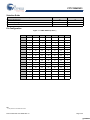
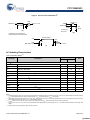
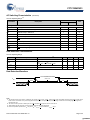
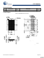
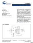
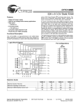
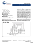
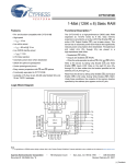
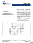
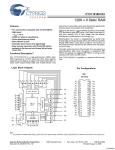
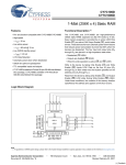
CY7C1024DV33
3-Mbit (128K X 24) Static RAM
Features
Functional Description
■
High speed
❐ tAA = 10 ns
■
Low active power
❐ ICC = 175 mA at 10 ns
The CY7C1024DV33 is a high performance CMOS static RAM
organized as 128K words by 24 bits. This device has an
automatic power down feature that significantly reduces power
consumption when deselected.
■
Low CMOS standby power
❐ ISB2 = 25 mA
To write to the device, enable the chip (CE1 LOW, CE2 HIGH,
and CE3 LOW), while forcing the Write Enable (WE) input LOW.
To read from the device, enable the chip by taking CE1 LOW, CE2
HIGH, and CE3 LOW while forcing the Output Enable (OE) LOW
and the Write Enable (WE) HIGH. See the Truth Table on page
7 for a complete description of Read and Write modes.
■
Operating voltages of 3.3 ± 0.3V
■
2.0V data retention
■
Automatic power down when deselected
■
TTL compatible inputs and outputs
■
Easy memory expansion with CE1, CE2, and CE3 features
■
Available in Pb-free standard 119-ball PBGA
The 24 I/O pins (I/O0 to I/O23) are placed in a high impedance
state when the device is deselected (CE1 HIGH, CE2 LOW, or
CE3 HIGH) or when the output enable (OE) is HIGH during a
write operation. (CE1 LOW, CE2 HIGH, CE3 LOW, and WE
LOW).
Logic Block Diagram
128K x 24
ARRAY
COLUMN
DECODER
I/O0 – I/O23
SENSE AMPS
A(9:0)
ROW DECODER
INPUT BUFFER
CONTROL LOGIC
CE1, CE2, CE3
WE
OE
A(16:10)
Cypress Semiconductor Corporation
Document Number: 001-08353 Rev. *C
•
198 Champion Court
•
San Jose, CA 95134-1709
•
408-943-2600
Revised November 6, 2008
[+] Feedback
CY7C1024DV33
Selection Guide
Description
–10
Unit
Maximum Access Time
10
ns
Maximum Operating Current
175
mA
Maximum CMOS Standby Current
25
mA
Pin Configuration
Figure 1. 119-Ball PBGA Top View [1]
1
2
3
4
5
6
7
A
NC
A
A
A
A
A
NC
B
NC
A
A
CE1
A
A
NC
C
I/O12
NC
CE2
NC
CE3
NC
I/O0
D
I/O13
VDD
VSS
VSS
VSS
VDD
I/O1
E
I/O14
VSS
VDD
VSS
VDD
VSS
I/O2
F
I/O15
VDD
VSS
VSS
VSS
VDD
I/O3
G
I/O16
VSS
VDD
VSS
VDD
VSS
I/O4
H
I/O17
VDD
VSS
VSS
VSS
VDD
I/O5
J
NC
VSS
VDD
VSS
VDD
VSS
NC
K
I/O18
VDD
VSS
VSS
VSS
VDD
I/O6
L
I/O19
VSS
VDD
VSS
VDD
VSS
I/O7
M
I/O20
VDD
VSS
VSS
VSS
VDD
I/O8
N
I/O21
VSS
VDD
VSS
VDD
VSS
I/O9
P
I/O22
VDD
VSS
VSS
VSS
VDD
I/O10
R
I/O23
NC
NC
NC
NC
NC
I/O11
T
NC
A
A
WE
A
A
NC
U
NC
A
A
OE
A
A
NC
Note
1. NC pins are not connected on the die.
Document Number: 001-08353 Rev. *C
Page 2 of 9
[+] Feedback
CY7C1024DV33
Maximum Ratings
DC Input Voltage [2] ............................... –0.5V to VCC + 0.5V
Exceeding maximum ratings may impair the useful life of the
device. These user guidelines are not tested.
Current into Outputs (LOW) ........................................ 20 mA
Storage Temperature ................................. –65°C to +150°C
(MIL-STD-883, Method 3015)
Ambient Temperature with
Power Applied ............................................ –55°C to +125°C
Latch Up Current ..................................................... >200 mA
Static Discharge Voltage............. ...............................>2001V
Operating Range
Supply Voltage on VCC Relative to GND [2] ....–0.5V to +4.6V
DC Voltage Applied to Outputs
in High Z State [2] ................................... –0.5V to VCC + 0.5V
Range
Ambient
Temperature
VCC
Industrial
–40°C to +85°C
3.3V ± 0.3V
DC Electrical Characteristics
Over the Operating Range
Parameter
Test Conditions [3]
Description
VOH
Output HIGH Voltage
VCC = Min, IOH = –4.0 mA
VOL
Output LOW Voltage
VCC = Min, IOL = 8.0 mA
VIH
Input HIGH Voltage
Input LOW Voltage
VIL
[2]
–10
Min
Max
Unit
2.4
V
0.4
V
2.0
VCC + 0.3
V
–0.3
0.8
V
IIX
Input Leakage Current
GND < VI < VCC
–1
+1
μA
IOZ
Output Leakage Current
GND < VOUT < VCC, output disabled
–1
+1
μA
ICC
VCC Operating Supply
Current
VCC = Max, f = fMAX = 1/tRC
IOUT = 0 mA CMOS levels
175
mA
ISB1
Automatic CE Power Down Max VCC, CE > VIH
Current —TTL Inputs
VIN > VIH or VIN < VIL, f = fMAX
Automatic CE Power Down Max VCC, CE > VCC – 0.3V,
Current — CMOS Inputs
VIN > VCC – 0.3V, or VIN < 0.3V, f = 0
30
mA
25
mA
ISB2
Capacitance
Tested initially and after any design or process changes that may affect these parameters.
Parameter
Description
CIN
Input Capacitance
COUT
I/O Capacitance
Test Conditions
TA = 25°C, f = 1 MHz, VCC = 3.3V
Max
Unit
8
pF
10
pF
119-Ball
PBGA
Unit
20.31
°C/W
8.35
°C/W
Thermal Resistance
Tested initially and after any design or process changes that may affect these parameters.
Parameter
Description
ΘJA
Thermal Resistance
(Junction to Ambient)
ΘJC
Thermal Resistance
(Junction to Case)
Test Conditions
Still air, soldered on a 3 × 4.5 inch,
four layer printed circuit board
Notes
2. VIL (min) = –2.0V and VIH(max) = VCC + 2V for pulse durations of less than 20 ns.
3. CE refers to a combination of CE1, CE2, and CE3. CE is LOW when CE1, CE3 are LOW and CE2 is HIGH. CE is HIGH when CE1 is HIGH, or CE2 is LOW, or CE3 is HIGH.
Document Number: 001-08353 Rev. *C
Page 3 of 9
[+] Feedback
CY7C1024DV33
Figure 2. AC Test Loads and Waveform[4]
50Ω
Z0 = 50Ω
R1 317 Ω
3.3V
VTH = 1.5V
OUTPUT
OUTPUT
30 pF*
R2
351Ω
5 pF*
*Including jig
(a)
and scope
(b)
*Capacitive Load consists of all
components of the test environment
All input pulses
3.0V
90%
10%
GND
90%
10%
Fall Time:> 1V/ns
Rise Time > 1V/ns
(c)
AC Switching Characteristics
Over the Operating Range [5]
Parameter
Description
–10
Min
Max
Unit
Read Cycle
tpower[6]
VCC(Typical) to the First Access
100
μs
tRC
Read Cycle Time
10
ns
tAA
Address to Data Valid
tOHA
Data Hold from Address Change
tACE
CE Active LOW to Data Valid [3]
10
ns
tDOE
OE LOW to Data Valid
5
ns
tLZOE
tHZOE
OE LOW to Low Z
10
[7]
OE HIGH to High Z
ns
1
[7]
[3, 7]
tLZCE
CE Active LOW to Low Z
tHZCE
CE Deselect HIGH to High Z [3, 7]
tPU
CE Active LOW to Power Up [3, 8]
tPD
3
CE Deselect HIGH to Power Down
ns
5
ns
5
ns
3
ns
0
[3, 8]
ns
ns
10
ns
Notes
4. Valid SRAM operation does not occur until the power supplies have reached the minimum operating VDD (3.0V). 100 μs (tpower) after reaching the minimum operating
VDD, normal SRAM operation can begin including reduction in VDD to the data retention (VCCDR, 2.0V) voltage.
5. Test conditions assume signal transition time of 3 ns or less, timing reference levels of 1.5V, and input pulse levels of 0 to 3.0V. Test conditions for the read cycle use
output loading as shown in part a) of Figure 2, unless specified otherwise.
6. tPOWER gives the minimum amount of time that the power supply is at typical VCC values until the first memory access is performed.
7. tHZOE, tHZCE, tHZWE, tLZOE, tLZCE, and tLZWE are specified with a load capacitance of 5 pF as in part (b) of Figure 2. Transition is measured ±200 mV from steady state
voltage.
8. These parameters are guaranteed by design and are not tested.
Document Number: 001-08353 Rev. *C
Page 4 of 9
[+] Feedback
CY7C1024DV33
AC Switching Characteristics
(continued)
Over the Operating Range [5]
Parameter
–10
Description
Min
Unit
Max
Write Cycle [9, 10]
tWC
Write Cycle Time
[3]
10
ns
7
ns
7
ns
tSCE
CE active LOW to Write End
tAW
Address Setup to Write End
tHA
Address Hold from Write End
0
ns
tSA
Address Setup to Write Start
0
ns
tPWE
WE Pulse Width
7
ns
tSD
Data Setup to Write End
5.5
ns
tHD
Data Hold from Write End
0
ns
tLZWE
WE HIGH to Low Z [7]
3
ns
tHZWE
WE LOW to High Z [7]
5
ns
Data Retention Characteristics
Over the Operating Range
Parameter
Conditions [3]
Description
VDR
VCC for Data Retention
ICCDR
Data Retention Current
tCDR [11]
Chip Deselect to Data Retention Time
tR
[12]
Min
Typ
Max
2
VCC = 2V, CE > VCC – 0.2V,
VIN > VCC – 0.2V or VIN < 0.2V
V
25
Operation Recovery Time
Unit
mA
0
ns
tRC
ns
Data Retention Waveform
DATA RETENTION MODE
VCC
3.0V
tCDR
VDR > 2V
3.0V
tR
CE
Notes
9. The internal write time of the memory is defined by the overlap of CE1 and CE2 and CE3 LOW and WE LOW. Chip enables must be active and WE must be LOW to
initiate a write. The transition of any of these signals terminate the write. The input data setup and hold timing is referenced to the leading edge of the signal that
terminates the write.
10. The minimum write cycle time for Write Cycle No. 3 (WE controlled, OE LOW) is the sum of tHZWE and tSD.
11. Tested initially and after any design or process changes that may affect these parameters.
12. Full device operation requires linear VCC ramp from VDR to VCC(min) > 50 μs or stable at VCC(min) > 50 μs.
Document Number: 001-08353 Rev. *C
Page 5 of 9
[+] Feedback
CY7C1024DV33
Switching Waveforms
Figure 3. Read Cycle No. 1 (Address Transition Controlled) [13, 14]
tRC
RC
ADDRESS
tAA
tOHA
DATA OUT
PREVIOUS DATA VALID
DATA VALID
Figure 4. Read Cycle No. 2 (OE Controlled) [3, 14, 15]
ADDRESS
tRC
CE
tACE
OE
tHZOE
tDOE
DATA OUT
tHZCE
tLZOE
HIGH IMPEDANCE
DATA VALID
tLZCE
VCC
SUPPLY
CURRENT
HIGH
IMPEDANCE
tPD
tPU
ICC
50%
50%
ISB
Figure 5. Write Cycle No. 1 (CE Controlled) [3, 16, 17]
tWC
ADDRESS
tSCE
CE
tSA
tSCE
tAW
tHA
tPWE
WE
tSD
DATA I/O
tHD
DATA VALID
Notes
13. Device is continuously selected. OE, CE = VIL.
14. WE is HIGH for read cycle.
15. Address valid before or similar to CE transition LOW.
16. Data I/O is high impedance if OE = VIH.
17. If CE goes HIGH simultaneously with WE going HIGH, the output remains in a high impedance state.
Document Number: 001-08353 Rev. *C
Page 6 of 9
[+] Feedback
CY7C1024DV33
Switching Waveforms (continued)
Figure 6. Write Cycle No. 2 (WE Controlled, OE HIGH During Write) [3, 16, 17]
tWC
ADDRESS
tSCE
CE
tAW
tHA
tSA
tPWE
WE
OE
tSD
DATA I/O
tHD
DATAIN VALID
NOTE 18
tHZOE
Figure 7. Write Cycle No. 3 (WE Controlled, OE LOW) [3, 17]
tWC
ADDRESS
tSCE
CE
tAW
tSA
tHA
tPWE
WE
tSD
DATA I/O
NOTE 18
tHD
DATA VALID
tLZWE
tHZWE
Truth Table
CE1
CE2
CE3
OE
WE
I/O0 – I/O23
Mode
Power
H
X
X
X
X
High Z
Power Down
Standby (ISB)
X
L
X
X
X
High Z
Power Down
Standby (ISB)
X
X
H
X
X
High Z
Power Down
Standby (ISB)
L
H
L
L
H
Full Data Out
Read
Active (ICC)
L
H
L
X
L
Full Data In
Write
Active (ICC)
L
H
L
H
H
High Z
Selected, Outputs Disabled Active (ICC)
Note
18. During this period, the I/Os are in the output state and input signals are not applied.
Document Number: 001-08353 Rev. *C
Page 7 of 9
[+] Feedback
CY7C1024DV33
Ordering Information
Speed
(ns)
10
Ordering Code
CY7C1024DV33-10BGXI
Package
Name
Package Type
Operating
Range
51-85115
119-Ball Plastic Ball Grid Array (14 x 22 x 2.4 mm) (Pb-Free)
Industrial
Package Diagram
Figure 8. 119-Ball PBGA (14 x 22 x 2.4 mm)
51-85115-*B
Document Number: 001-08353 Rev. *C
Page 8 of 9
[+] Feedback
CY7C1024DV33
Document History Page
Document Title: CY7C1024DV33, 3-Mbit (128K X 24) Static RAM
Document Number: 001-08353
Rev.
ECN No.
Orig. of
Change
Submission
Date
**
469517
NXR
See ECN
New data sheet
*A
499604
NXR
See ECN
Added note 1 for NC pins
Changed ICC specification from 150 mA to 185 mA
Updated Test Condition for ICC in DC Electrical Characteristics table
Added note for tACE, tLZCE, tHZCE, tPU, tPD, tSCE in AC Switching Characteristics Table
on page 4
*B
1462586
VKN/SFV
See ECN
Converted from preliminary to final
Updated block diagram
Changed ICC specification from 185 mA to 225 mA
Updated thermal specs
*C
2604677
VKN/PYRS
11/12/08
Removed Commercial operating range, Added Industrial operating range
Removed 8 ns speed bin, Added 10 ns speed bin
Description of Change
Sales, Solutions, and Legal Information
Worldwide Sales and Design Support
Cypress maintains a worldwide network of offices, solution centers, manufacturer’s representatives, and distributors. To find the office
closest to you, visit us at cypress.com/sales.
Products
PSoC Solutions
PSoC
psoc.cypress.com
Clocks & Buffers
clocks.cypress.com
General
Low Power/Low Voltage
psoc.cypress.com/solutions
psoc.cypress.com/low-power
Wireless
wireless.cypress.com
Precision Analog
Memories
memory.cypress.com
LCD Drive
psoc.cypress.com/lcd-drive
image.cypress.com
CAN 2.0b
psoc.cypress.com/can
USB
psoc.cypress.com/usb
Image Sensors
psoc.cypress.com/precision-analog
© Cypress Semiconductor Corporation, 2006-2008. The information contained herein is subject to change without notice. Cypress Semiconductor Corporation assumes no responsibility for the use
of any circuitry other than circuitry embodied in a Cypress product. Nor does it convey or imply any license under patent or other rights. Cypress products are not warranted nor intended to be used
for medical, life support, life saving, critical control or safety applications, unless pursuant to an express written agreement with Cypress. Furthermore, Cypress does not authorize its products for use
as critical components in life-support systems where a malfunction or failure may reasonably be expected to result in significant injury to the user. The inclusion of Cypress products in life-support
systems application implies that the manufacturer assumes all risk of such use and in doing so indemnifies Cypress against all charges.
Any Source Code (software and/or firmware) is owned by Cypress Semiconductor Corporation (Cypress) and is protected by and subject to worldwide patent protection (United States and foreign),
United States copyright laws and international treaty provisions. Cypress hereby grants to licensee a personal, non-exclusive, non-transferable license to copy, use, modify, create derivative works of,
and compile the Cypress Source Code and derivative works for the sole purpose of creating custom software and or firmware in support of licensee product to be used only in conjunction with a Cypress
integrated circuit as specified in the applicable agreement. Any reproduction, modification, translation, compilation, or representation of this Source Code except as specified above is prohibited without
the express written permission of Cypress.
Disclaimer: CYPRESS MAKES NO WARRANTY OF ANY KIND, EXPRESS OR IMPLIED, WITH REGARD TO THIS MATERIAL, INCLUDING, BUT NOT LIMITED TO, THE IMPLIED WARRANTIES
OF MERCHANTABILITY AND FITNESS FOR A PARTICULAR PURPOSE. Cypress reserves the right to make changes without further notice to the materials described herein. Cypress does not
assume any liability arising out of the application or use of any product or circuit described herein. Cypress does not authorize its products for use as critical components in life-support systems where
a malfunction or failure may reasonably be expected to result in significant injury to the user. The inclusion of Cypress’ product in a life-support systems application implies that the manufacturer
assumes all risk of such use and in doing so indemnifies Cypress against all charges.
Use may be limited by and subject to the applicable Cypress software license agreement.
Document Number: 001-08353 Rev. *C
Revised November 6, 2008
Page 9 of 9
All product and company names mentioned in this document are the trademarks of their respective holders.
[+] Feedback