1
CY7C1024DV33
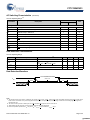
AC Switching Characteristics
(continued)
Over the Operating Range [5]
Parameter
–10
Description
Min
Unit
Max
Write Cycle [9, 10]
tWC
Write Cycle Time
[3]
10
ns
7
ns
7
ns
tSCE
CE active LOW to Write End
tAW
Address Setup to Write End
tHA
Address Hold from Write End
0
ns
tSA
Address Setup to Write Start
0
ns
tPWE
WE Pulse Width
7
ns
tSD
Data Setup to Write End
5.5
ns
tHD
Data Hold from Write End
0
ns
tLZWE
WE HIGH to Low Z [7]
3
ns
tHZWE
WE LOW to High Z [7]
5
ns
Data Retention Characteristics
Over the Operating Range
Parameter
Conditions [3]
Description
VDR
VCC for Data Retention
ICCDR
Data Retention Current
tCDR [11]
Chip Deselect to Data Retention Time
tR
[12]
Min
Typ
Max
2
VCC = 2V, CE > VCC – 0.2V,
VIN > VCC – 0.2V or VIN < 0.2V
V
25
Operation Recovery Time
Unit
mA
0
ns
tRC
ns
Data Retention Waveform
DATA RETENTION MODE
VCC
3.0V
tCDR
VDR > 2V
3.0V
tR
CE
Notes
9. The internal write time of the memory is defined by the overlap of CE1 and CE2 and CE3 LOW and WE LOW. Chip enables must be active and WE must be LOW to
initiate a write. The transition of any of these signals terminate the write. The input data setup and hold timing is referenced to the leading edge of the signal that
terminates the write.
10. The minimum write cycle time for Write Cycle No. 3 (WE controlled, OE LOW) is the sum of tHZWE and tSD.
11. Tested initially and after any design or process changes that may affect these parameters.
12. Full device operation requires linear VCC ramp from VDR to VCC(min) > 50 μs or stable at VCC(min) > 50 μs.
Document Number: 001-08353 Rev. *C
Page 5 of 9
[+] Feedback