1
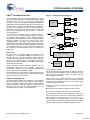
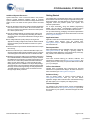
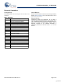
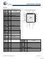
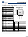
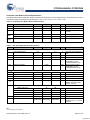
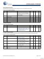
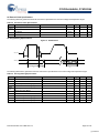
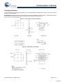
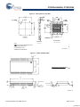
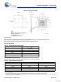
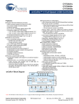
CY8C20x36/46/66, CY8C20396
CapSense™ Applications
Features
■
1.71V to 5.5V Operating Range
■
Low Power CapSense™ Block
❐ Configurable Capacitive Sensing Elements
❐ Supports Combination of CapSense Buttons, Sliders,
Touchpads, Touch Screens, and Proximity Sensor
■
Powerful Harvard Architecture Processor
❐ M8C Processor Speeds Running to 24 MHz
❐ Low Power at High Speed
❐ Interrupt Controller
❐ Temperature Range: -40°C to +85°C
■
Flexible On-Chip Memory
❐ Three Program/Data Storage Size Options:
• CY8C20x36: 8K Flash / 1K SRAM
• CY8C20x46: 16K Flash / 2K SRAM
• CY8C20x66: 32K Flash / 2K SRAM
❐ 50,000 Flash Erase/Write Cycles
❐ Partial Flash Updates
❐ Flexible Protection Modes
❐ In-System Serial Programming (ISSP)
■
Full-Speed USB
❐ Available on CY8C20396 and CY8C20666 Only
❐ 12 Mbps USB 2.0 Compliant
❐ Eight Unidirectional Endpoints
❐ One Bidirectional Control Endpoint
❐ Dedicated 512 Byte Buffer
❐ Internally Regulated at 3.3V
■
Precision, Programmable Clocking
❐ Internal Main Oscillator: 6/12/24 MHz ± 5%
❐ Internal Low Speed Oscillator at 32 kHz for Watchdog and
Sleep Timers
❐ Precision 32 kHz Oscillator for Optional External Crystal
(CY8C20x46/66 only)
❐ 0.25% Accuracy for USB with No External Components
(CY8C20396 and CY8C20666 only)
■
Programmable Pin Configurations
❐ Up to 36 GPIO (Depending on Package)
❐ Dual Mode GPIO: All GPIO Support Digital IO and Analog
Input
❐ 25 mA Sink Current on All GPIO
❐ Pull up, High Z, Open Drain Modes on All GPIO
❐ CMOS Drive Mode(5 mA Source Current) on Ports 0 and 1:
• 20 mA (at 3.0V) Total Source Current on Port 0
• 20 mA (at 3.0V) Total Source Current on Port 1
❐ Selectable, Regulated Digital IO on Port 1
❐ Configurable Input Threshold on Port 1
❐ Hot Swap Capability on all Port 1 GPIO
Cypress Semiconductor Corporation
Document Number: 001-12696 Rev. *D
•
■
Versatile Analog Mux
❐ Common Internal Analog Bus
❐ Simultaneous Connection of IO
❐ High PSRR Comparator
❐ Low Dropout Voltage Regulator for All Analog Resources
■
Additional System Resources
2
❐ I C™ Slave:
• Selectable to 50 kHz, 100 kHz, or 400 kHz
• No Clock Stretching Required (under most conditions)
• Implementation During Sleep Modes with Less Than
100 µA
• Hardware Address Validation
❐ SPI™ Master and Slave: Configurable 46.9 kHz - 12 MHz
❐ Three 16-Bit Timers
❐ Watchdog and Sleep Timers
❐ Internal Voltage Reference
❐ Integrated Supervisory Circuit
■
Complete Development Tools
❐ Free Development Tool (PSoC Designer™)
❐ Full Featured, In-Circuit Emulator and Programmer
❐ Full Speed Emulation
❐ Complex Breakpoint Structure
❐ 128K Trace Memory
■
Package Options
❐ CY8C20x36:
• 16-Pin 3 x 3 x 0.6 mm QFN
• 24-Pin 4 x 4 x 0.6 mm QFN
• 32-Pin 5 x 5 x 0.6 mm QFN
❐ CY8C20x46:
• 16-Pin 3 x 3 x 0.6 mm QFN
• 24-Pin 4 x 4 x 0.6 mm QFN
• 32-Pin 5 x 5 x 0.6 mm QFN
❐ CY8C20396: 24-Pin 4 x 4 x 0.6 mm QFN
❐ CY8C20x66:
• 32-Pin 5 x 5 x 0.6 mm QFN
• 48-Pin 7 x 7 x 1.0 mm QFN (with USB)
• 48-Pin SSOP
198 Champion Court
•
San Jose, CA 95134-1709
•
408-943-2600
Revised March 17, 2009
[+] Feedback
CY8C20x36/46/66, CY8C20396
Block Diagram
Port 4
Port 3
Port 2
Port 1
Port 0
1.8/2.5/3V
LDO
PWRSYS
(Regulator)
PSoC CORE
SYSTEM BUS
Global Analog Interconnect
1K/2K
SRAM
Supervisory ROM (SROM)
Interrupt
Controller
8K/16K/32K Flash
Nonvolatile Memory
Sleep and
Watchdog
CPU Core (M8C)
6/12/24 MHz Internal Main Oscillator
(IMO)
Internal Low Speed Oscillator (ILO)
Multiple Clock Sources
CAPSENSE
SYSTEM
Analog
Reference
CapSense
Module
Two
Comparators
Analog
Mux
SYSTEM BUS
USB
I2C
Slave
Internal
Voltage
References
System
Resets
POR
and
LVD
SPI
Master/
Slave
Three 16-Bit
Programmable
Timers
Digital
Clocks
SYSTEM RESOURCES
Document Number: 001-12696 Rev. *D
Page 2 of 34
[+] Feedback
CY8C20x36/46/66, CY8C20396
PSoC® Functional Overview
Figure 1. Analog System Block Diagram
The PSoC family consists of on-chip Controller devices. These
devices are designed to replace multiple traditional MCU-based
components with one, low cost single-chip programmable
component. A PSoC device includes configurable analog and
digital blocks, and programmable interconnect. This architecture
allows the user to create customized peripheral configurations,
to match the requirements of each individual application.
Additionally, a fast CPU, Flash program memory, SRAM data
memory, and configurable IO are included in a range of
convenient pinouts.
Analog Global Bus
IDAC
Vr
The architecture for this device family, as shown in the Block
Diagram on page 2, is comprised of three main areas: the Core,
the CapSense Analog System, and the System Resources
(including a full speed USB port). A common, versatile bus allows
connection between IO and the analog system. Each
CY8C20x36/46/66, CY8C20396 PSoC device includes a
dedicated CapSense block that provides sensing and scanning
control circuitry for capacitive sensing applications. Depending
on the PSoC package, up to 36 general purpose IO (GPIO) are
also included. The GPIO provides access to the MCU and
analog mux.
Reference
Buffer
Cinternal
Comparator
Mux
Mux
Refs
PSoC Core
CapSenseCounters
The PSoC Core is a powerful engine that supports a rich
instruction set. It encompasses SRAM for data storage, an
interrupt controller, sleep and watchdog timers, and IMO
(internal main oscillator) and ILO (internal low speed oscillator).
The CPU core, called the M8C, is a powerful processor with
speeds up to 24 MHz. The M8C is a four-MIPS, 8-bit Harvard
architecture microprocessor.
System Resources provide additional capability, such as
configurable USB and I2C slave/SPI master-slave
communication interface, three 16-bit programmable timers, and
various system resets supported by the M8C.
The Analog System is composed of the CapSense PSoC block
and an internal 1.2V analog reference, which together support
capacitive sensing of up to 36 inputs.
CapSense Analog System
The Analog System contains the capacitive sensing hardware.
Several hardware algorithms are supported. This hardware
performs capacitive sensing and scanning without requiring
external components. Capacitive sensing is configurable on
each GPIO pin. Scanning of enabled CapSense pins are
completed quickly and easily across multiple ports.
CSCLK
IMO
CapSense
Clock Select
Oscillator
Analog Multiplexer System
The Analog Mux Bus can connect to every GPIO pin. Pins are
connected to the bus individually or in any combination. The bus
also connects to the analog system for analysis with the
CapSense block comparator.
Switch control logic enables selected pins to precharge
continuously under hardware control. This enables capacitive
measurement for applications such as touch sensing. Other
multiplexer applications include:
■
Complex capacitive sensing interfaces, such as sliders and
touchpads.
■
Chip-wide mux that allows analog input from any IO pin.
■
Crosspoint connection between any IO pin combinations.
When designing capacitive sensing applications, refer to the
latest signal-to-noise signal level requirements Application
Notes, which can be found under http://www.cypress.com >>
Documentation >> Application Notes. In general, and unless
otherwise noted in the relevant Application Notes, the minimum
signal-to-noise ratio (SNR) for CapSense applications is 5:1.
Document Number: 001-12696 Rev. *D
Page 3 of 34
[+] Feedback
CY8C20x36/46/66, CY8C20396
Additional System Resources
System Resources, some of which are listed in the previous
sections, provide additional capability useful to complete
systems. Additional resources include low voltage detection and
power on reset. The merits of each system resource are listed
here:
Getting Started
The quickest way to understand PSoC silicon is to read this data
sheet and then use the PSoC Designer Integrated Development
Environment (IDE). This data sheet is an overview of the PSoC
integrated circuit and presents specific pin, register, and
electrical specifications.
■
The I2C slave/SPI master-slave module provides 50/100/400
kHz communication over two wires. SPI communication over
three or four wires runs at speeds of 46.9 kHz to 3 MHz (lower
for a slower system clock).
■
The I2C hardware address recognition feature reduces the
already low power consumption by eliminating the need for
CPU intervention until a packet addressed to the target device
is received.
Application Notes
■
Low Voltage Detection (LVD) interrupts can signal the
application of falling voltage levels, while the advanced POR
(Power-On-Reset) circuit eliminates the need for a system
supervisor.
Application notes are an excellent introduction to the wide variety
of possible PSoC designs. They are located here:
www.cypress.com/psoc. Select Application Notes under the
Documentation tab.
■
An internal reference provides an absolute reference for capacitive sensing.
Development Kits
■
The 5.5V maximum input, 1.8/2.5/3V-selectable output, lowdropout regulator (LDO) provides regulation for IOs. A registercontrolled bypass mode allows the user to disable the LDO.
■
Standard Cypress PSoC IDE tools are available for debugging
the CY8C20x36/46/66, CY8C20396 family of parts. However,
the additional trace length and a minimal ground plane in the
Flex-Pod can create noise problems that make it difficult to
debug a Power PSoC design. A custom bonded On-Chip
Debug (OCD) device is available in an 48-pin QFN package.
The OCD device is recommended for debugging designs that
have high current and/or high analog accuracy requirements.
The QFN package is compact and is connected to the ICE
through a high density connector.
For in depth information, along with detailed programming
details, see the PSoC® Programmable System-on-Chip™
Technical Reference Manual for CY8C28xxx PSoC devices.
For up-to-date ordering, packaging, and electrical specification
information, see the latest PSoC device data sheets on the web
at www.cypress.com/psoc.
PSoC Development Kits are available online from Cypress at
www.cypress.com/shop and through a growing number of
regional and global distributors, which include Arrow, Avnet, DigiKey, Farnell, Future Electronics, and Newark.
Training
Free PSoC technical training (on demand, webinars, and
workshops) is available online at www.cypress.com/training. The
training covers a wide variety of topics and skill levels to assist
you in your designs.
CYPros Consultants
Certified PSoC Consultants offer everything from technical
assistance to completed PSoC designs. To contact or become a
PSoC Consultant go to www.cypress.com/cypros.
Solutions Library
Visit our growing library of solution focused designs at
www.cypress.com/solutions. Here you can find various
application designs that include firmware and hardware design
files that enable you to complete your designs quickly.
Technical Support
For assistance with technical issues, search KnowledgeBase
articles and forums at www.cypress.com/support. If you cannot
find an answer to your question, call technical support at 1-800541-4736.
Document Number: 001-12696 Rev. *D
Page 4 of 34
[+] Feedback
CY8C20x36/46/66, CY8C20396
Development Tools
PSoC Designer™ is a Microsoft® Windows-based, integrated
development environment for the Programmable System-onChip (PSoC) devices. The PSoC Designer IDE and application
runs on Windows XP and Windows Vista.
This system provides design database management by project,
an integrated debugger with In-Circuit Emulator, in-system
programming support, and built-in support for third-party assemblers and C compilers.
PSoC Designer also supports C language compilers developed
specifically for the devices in the PSoC family.
PSoC Designer Software Subsystems
System-Level View
The system-level view is a drag-and-drop visual embedded
system design environment based on PSoC Express. In this
view you solve design problems the same way you might think
about the system. Select input and output devices based upon
system requirements. Add a communication interface and define
the interface to the system (registers). Define when and how an
output device changes state based upon any/all other system
devices. Based upon the design, PSoC Designer automatically
selects one or more PSoC devices that match your system
requirements.
PSoC Designer generates all embedded code, then compiles
and links it into a programming file for a specific PSoC device.
Chip-Level View
The chip-level view is a more traditional integrated development
environment (IDE) based on PSoC Designer 4.x. You choose a
base device to work with and then select different onboard
analog and digital components called user modules that use the
PSoC blocks. Examples of user modules are ADCs, DACs,
Amplifiers, and Filters. You configure the user modules for your
chosen application and connect them to each other and to the
proper pins. Then you generate your project. This prepopulates
your project with APIs and libraries that you can use to program
your application.
The tool also supports easy development of multiple configurations and dynamic reconfiguration. Dynamic reconfiguration
allows for changing configurations at run time.
Hybrid Designs
You can begin in the system-level view, allow it to choose and
configure your user modules, routing, and generate code, then
switch to the chip-level view to gain complete control over onchip resources. All views of the project share common code
editor, builder, and common debug, emulation, and programming
tools.
Document Number: 001-12696 Rev. *D
Code Generation Tools
PSoC Designer supports multiple third-party C compilers and
assemblers. The code generation tools work seamlessly within
the PSoC Designer interface and have been tested with a full
range of debugging tools. The choice is yours.
Assemblers. The assemblers allow assembly code to be
merged seamlessly with C code. Link libraries automatically use
absolute addressing or are compiled in relative mode, and linked
with other software modules to get absolute addressing.
C Language Compilers. C language compilers are available
that support the PSoC family of devices. The products allow you
to create complete C programs for the PSoC family devices.
The optimizing C compilers provide all the features of C tailored
to the PSoC architecture. They come complete with embedded
libraries providing port and bus operations, standard keypad and
display support, and extended math functionality.
Debugger
PSoC Designer has a debug environment that provides
hardware in-circuit emulation, allowing you to test the program in
a physical system while providing an internal view of the PSoC
device. Debugger commands allow the designer to read and
program and read and write data memory, read and write IO
registers, read and write CPU registers, set and clear breakpoints, and provide program run, halt, and step control. The
debugger also allows the designer to create a trace buffer of
registers and memory locations of interest.
Online Help System
The online help system displays online, context-sensitive help
for the user. Designed for procedural and quick reference, each
functional subsystem has its own context-sensitive help. This
system also provides tutorials and links to FAQs and an Online
Support Forum to aid the designer in getting started.
In-Circuit Emulator
A low cost, high functionality ICE (In-Circuit Emulator) is
available for development support. This hardware has the
capability to program single devices.
The emulator consists of a base unit that connects to the PC by
way of a USB port. The base unit is universal and operates with
all PSoC devices. Emulation pods for each device family are
available separately. The emulation pod takes the place of the
PSoC device in the target board and performs full speed (24
MHz) operation.
Page 5 of 34
[+] Feedback
CY8C20x36/46/66, CY8C20396
Designing with PSoC Designer
The development process for the PSoC device differs from that
of a traditional fixed function microprocessor. The configurable
analog and digital hardware blocks give the PSoC architecture a
unique flexibility that pays dividends in managing specification
change during development and by lowering inventory costs.
These configurable resources, called PSoC Blocks, have the
ability to implement a wide variety of user-selectable functions.
The PSoC development process can be summarized in the
following four steps:
1. Select Components
2. Configure Components
3. Organize and Connect
4. Generate, Verify, and Debug
Select Components
Organize and Connect
You build signal chains at the chip level by interconnecting user
modules to each other and the IO pins, or connect system-level
inputs, outputs, and communication interfaces to each other with
valuator functions.
In the system-level view selecting a potentiometer driver to
control a variable speed fan driver and setting up the valuators
to control the fan speed based on input from the pot selects,
places, routes, and configures a programmable gain amplifier
(PGA) to buffer the input from the potentiometer, an analog-todigital converter (ADC) to convert the potentiometer’s output to
a digital signal, and a PWM to control the fan.
In the chip-level view, you perform the selection, configuration,
and routing so that you have complete control over the use of all
on-chip resources.
Both the system-level and chip-level views provide a library of
pre-built, pre-tested hardware peripheral components. In the
system-level view these components are called “drivers” and
correspond to inputs (a thermistor, for example), outputs (a
brushless DC fan, for example), communication interfaces (I2Cbus, for example), and the logic to control how they interact with
one another (called valuators).
Generate, Verify, and Debug
In the chip-level view the components are called “user modules.”
User modules make selecting and implementing peripheral
devices simple, and come in analog, digital, and programmable
system-on-chip varieties.
Both system-level and chip-level designs generate software
based on your design. The chip-level design provides application
programming interfaces (APIs) with high-level functions to
control and respond to hardware events at run time and interrupt
service routines that you can adapt as needed. The system-level
design also generates a C main() program that completely
controls the chosen application and contains placeholders for
custom code at strategic positions allowing you to further refine
the software without disrupting the generated code.
Configure Components
Each of the components you select establishes the basic register
settings that implement the selected function. They also provide
parameters and properties that allow you to tailor their precise
configuration to your particular application. For example, a Pulse
Width Modulator (PWM) User Module configures one or more
digital PSoC blocks, one for each 8 bits of resolution. The user
module parameters permit you to establish the pulse width and
duty cycle. Configure the parameters and properties to correspond to your chosen application. Enter values directly or by
selecting values from drop-down menus.
Both the system-level drivers and chip-level user modules are
documented in data sheets that are viewed directly in PSoC
Designer. These data sheets explain the internal operation of the
component and provide performance specifications. Each data
sheet describes the use of each user module parameter or driver
property, and other information you may need to successfully
implement your design.
Document Number: 001-12696 Rev. *D
When you are ready to test the hardware configuration or move
on to developing code for the project, you perform the “Generate
Configuration Files” step. This causes PSoC Designer to
generate source code that automatically configures the device to
your specification and provides the software for the system.
A complete code development environment allows you to
develop and customize your applications in C, assembly
language, or both.
The last step in the development process takes place inside
PSoC Designer’s Debugger (access by clicking the Connect
icon). PSoC Designer downloads the HEX image to the In-Circuit
Emulator (ICE) where it runs at full speed. PSoC Designer
debugging capabilities rival those of systems costing many times
more. In addition to traditional single-step, run-to-breakpoint and
watch-variable features, the debug interface provides a large
trace buffer and allows you to define complex breakpoint events
that include monitoring address and data bus values, memory
locations and external signals.
Page 6 of 34
[+] Feedback
CY8C20x36/46/66, CY8C20396
Document Conventions
Acronyms Used
Units of Measure
The following table lists the acronyms that are used in this
document.
A units of measure table is located in the Electrical Specifications
section. Table 9 on page 15 lists all the abbreviations used to
measure the PSoC devices.
Table 1. Acronyms
Acronym
Description
AC
alternating current
API
application programming interface
CPU
central processing unit
DC
direct current
FSR
full scale range
GPIO
general purpose IO
GUI
graphical user interface
ICE
in-circuit emulator
ILO
internal low speed oscillator
IMO
internal main oscillator
IO
input/output
LSb
least-significant bit
LVD
low voltage detect
MSb
most-significant bit
POR
power on reset
PPOR
precision power on reset
PSoC®
Programmable System-on-Chip™
SLIMO
slow IMO
SRAM
static random access memory
Document Number: 001-12696 Rev. *D
Numeric Naming
Hexadecimal numbers are represented with all letters in
uppercase with an appended lowercase ‘h’ (for example, ‘14h’ or
‘3Ah’). Hexadecimal numbers may also be represented by a ‘0x’
prefix, the C coding convention. Binary numbers have an
appended lowercase ‘b’ (for example, 01010100b’ or
‘01000011b’). Numbers not indicated by an ‘h’, ‘b’, or 0x are
decimal.
Page 7 of 34
[+] Feedback
CY8C20x36/46/66, CY8C20396
Pinouts
The CY8C20x36/46/66, CY8C20396 PSoC device is available in a variety of packages which are listed and illustrated in the following
tables. Every port pin (labeled with a “P”) is capable of Digital IO and connection to the common analog bus. However, Vss, Vdd, and
XRES are not capable of Digital IO.
16-Pin QFN
Table 2. Pin Definitions - CY8C20236, CY8C20246 PSoC Device [2]
P1[7] I2C SCL, SPI SS
4
IOHR
I
P1[5] I2C SDA, SPI MISO
5
IOHR
I
P1[3] SPI CLK
6
IOHR
I
P1[1] ISSP CLK[1], I2C SCL, SPI
MOSI
7
Power
Vss
Ground connection
8
IOHR
I
P1[0] ISSP DATA[1], I2C SDA, SPI
CLK
9
IOHR
I
P1[2]
10
IOHR
I
P1[4] Optional external clock
(EXTCLK)
11
12
13
Input
IOH
AI, XOut, P2[5]
AI, XIn, P2[3]
AI, I2C SCL, SPI SS, P1[7]
AI, I2C SDA, SPI MISO, P1[5]
1
2
3
4
I
12
QFN
(Top View) 11
XRES Active high external reset with
internal pull down
Power
14
13
P2[3] Crystal input (XIn)
I
10
9
8
I
IOHR
7
IO
3
Vss
2
AI, DATA1, I2C SDA, SPI CLK, P1[0]
P2[5] Crystal output (XOut)
P0[1], AI
P0[3], AI
P0[7], AI
Vdd
I
Figure 2. CY8C20236, CY8C20246 PSoC Device
16
15
Analog
IO
Description
5
6
Digital
1
Name
AI, SPI CLK, P1[3]
AI, CLK1, SPI MOSI, P1[1]
Type
Pin
No.
P0[4], AI
XRES
P1[4], EXTCLK, AI
P1[2], AI
P0[4]
Vdd
Supply voltage
14
IOH
I
P0[7]
15
IOH
I
P0[3] Integrating input
16
IOH
I
P0[1] Integrating input
LEGEND A = Analog, I = Input, O = Output, OH = 5 mA High Output Drive, R = Regulated Output.
Notes
1. These are the ISSP pins, which are not High Z at POR (Power On Reset).
2. During power up or reset event, device P1[1] and P1[0] may disturb the I2C bus. Use alternate pins if you encounter any issues.
Document Number: 001-12696 Rev. *D
Page 8 of 34
[+] Feedback
CY8C20x36/46/66, CY8C20396
24-Pin QFN
Table 3. Pin Definitions - CY8C20336, CY8C20346 [2, 3]
I
P1[7]
I2C SCL, SPI SS
5
IOHR
I
P1[5]
I2C SDA, SPI MISO
6
IOHR
I
P1[3]
SPI CLK
7
IOHR
I
P1[1]
ISSP CLK[1], I2C SCL, SPI
MOSI
8
9
Power
NC
No connection
Vss
Ground connection
ISSP DATA[1], I2C SDA, SPI
CLK
10
IOHR
I
P1[0]
11
IOHR
I
P1[2]
12
IOHR
I
P1[4]
13
IOHR
I
P1[6]
14
Input
XRES
15
IO
I
P2[0]
16
IOH
I
P0[0]
17
IOH
I
P0[2]
18
IOH
I
P0[4]
19
IOH
I
P0[6]
20
Power
Vdd
1
18
17
2
3
QFN
16
4
(Top View)
15
5
14
6
13
P0[4], AI
P0[2], AI
P0[0], AI
P2[0], AI
XRES
P1[6], AI
Active high external reset with
internal pull down
Supply voltage
IOH
I
P0[7]
22
IOH
I
P0[5]
23
IOH
I
P0[3]
Integrating input
24
IOH
I
P0[1]
Integrating input
Vss
Center pad must be connected
to ground
Power
AI, P2[1]
AI, I2C SCL, SPI SS, P1[7]
AI, I2C SDA, SPI MISO, P1[5]
AI, SPI CLK, P1[3]
Optional external clock input
(EXTCLK)
21
CP
AI, XOut, P2[5]
AI, XIn, P2[3]
19
IOHR
21
4
20
Crystal input (XIn)
P2[1]
11
12
P2[3]
I
22
I
IO
9
IO
3
10
2
AI, DATA2, I2C SDA, SPI CLK, P1[0]
AI, P1[2]
AI, EXTCLK, P1[4]
Crystal output (XOut)
P0[1], AI
P0[3], AI
P0[5], AI
P0[7], AI
Vdd
P0[6], AI
P2[5]
24
I
23
IO
8
1
Figure 3. CY8C20336, CY8C20346 PSoC Device
7
Description
AI, CLK2, I2C SCL
SPI MOSI, P1[1]
NC
Vss
Type
Pin
No. Digital Analog Name
LEGEND A = Analog, I = Input, O = Output, OH = 5 mA High Output Drive, R = Regulated Output.
Note
3. The center pad (CP) on the QFN package must be connected to ground (Vss) for best mechanical, thermal, and electrical performance. If not connected to ground, it
must be electrically floated and not connected to any other signal.
Document Number: 001-12696 Rev. *D
Page 9 of 34
[+] Feedback
CY8C20x36/46/66, CY8C20396
24-Pin QFN with USB Pinout
Table 4. Pin Definitions - CY8C20396 PSoC Device [2, 3]
Name
Description
1
IO
I
P2[5]
2
IO
I
P2[3]
3
IO
I
P2[1]
4
IOHR
I
P1[7]
I2C SCL, SPI SS
5
IOHR
I
P1[5]
I2C SDA, SPI MISO
6
IOHR
I
P1[3]
SPI CLK
7
IOHR
I
P1[1]
ISSP CLK, I2C SCL, SPI MOSI
8
VSS
Ground
9
IO
I
D+
USB D+
10
IO
I
D-
USB D-
11
Power
Power
VDD
Supply
12
IOHR
I
P1[0]
ISSP DATA, I2C SDA
13
IOHR
I
P1[2]
14
IOHR
I
P1[4]
15
IOHR
I
16
RESET INPUT
Optional external clock input
(EXTCLK)
P1[6]
XRES
IOH
I
P0[0]
18
IOH
I
P0[2]
19
IOH
I
P0[4]
20
IOH
I
P0[6]
21
IOH
I
P0[7]
22
IOH
I
P0[5]
23
IOH
I
P0[3]
Integrating input
24
IOH
I
P0[1]
Integrating input
VSS
Thermal pad must be
connected to Ground
Power
19
21
20
22
24
23
18
17
2
3
QFN
16
4
(Top View)
15
13
11
12
14
6
9
5
10
P2[1]
I2C SCL, SPI SS, P1[7]
I2C SDA, SPI MISO, P1[5]
SPI CLK, P1[3]
1
8
P2[5]
P2[3]
P0[2]
P0[0]
XRES
P1[6]
P1[4], EXTCLK
P1[2]
Active high external reset with
internal pull down
17
CP
Figure 4. CY8C20396 PSoC Device
P0[1], AI
P0[3]
P0[5]
P0[7]
P0[6]
P0[4]
Analog
7
Type
Digital
ISSP CLK, I2C SCL, SPI MOSI, P1[1]
Vss
USB D+
USB DVDD
ISSP DATA, I2C SDA, P1[0]
Pin No.
LEGEND I = Input, O = Output, OH = 5 mA High Output Drive, R = Regulated Output
Document Number: 001-12696 Rev. *D
Page 10 of 34
[+] Feedback
CY8C20x36/46/66, CY8C20396
32-Pin QFN
Table 5. Pin Definitions - CY8C20436/46/66 PSoC Device [2, 3]
P2[3]
Crystal input (XIn)
5
IO
I
P2[1]
6
IO
I
P3[3]
7
IO
I
P3[1]
8
IOHR
I
P1[7]
I2C SCL, SPI SS
9
IOHR
I
P1[5]
I2C SDA, SPI MISO
10
IOHR
I
P1[3]
SPI CLK.
11
IOHR
I
P1[1]
ISSP CLK[1], I2C SCL, SPI MOSI.
12
Vss
Ground connection.
13
IOHR
Power
I
P1[0]
ISSP DATA[1], I2C SDA., SPI CLK
14
IOHR
I
P1[2]
15
IOHR
I
P1[4]
16
IOHR
I
P1[6]
17
Input
XRES
18
IO
I
P3[0]
19
IO
I
P3[2]
20
IO
I
P2[0]
21
IO
I
P2[2]
22
IO
I
P2[4]
23
IO
I
P2[6]
24
IOH
I
P0[0]
25
IOH
I
P0[2]
26
IOH
I
P0[4]
27
IOH
I
P0[6]
28
Power
Vdd
29
IOH
I
P0[7]
30
IOH
I
P0[5]
31
IOH
I
AI, P0[1]
AI, P2[7]
AI, XOut, P2[5]
AI, XIn, P2[3]
AI, P2[1]
AI, P3[3]
AI, P3[1]
AI, I2C SCL, SPI SS, P1[7]
Optional external clock input
(EXTCLK)
Active high external reset with
internal pull down
1
2
3
4
5
6
7
8
P0 [4 ], AI
P0 [2 ], AI
I
26
25
IO
QFN
(Top View)
24
23
22
21
20
19
18
17
15
16
Crystal output (XOut)
4
AI, E XTCLK , P 1[4]
AI, P 1[6]
P2[5]
P0 [7 ], AI
Vd d
P0 [6 ], AI
P2[7]
I
28
27
I
IO
13
14
IO
3
30
29
2
Integrating input
AI, CLK4, I2C SCL, SPI MOSI, P1[1]
V ss
AI, DATA1, I2C SDA, SPI CLK, P1[0]
AI, P 1[2]
I
Vss
P0 [3 ], AI
P0 [5 ], AI
IOH
32
31
1
P0[1]
Figure 5. CY8C20436/46/66 PSoC Device
Description
9
Name
Analog
10
11
12
Type
Digital
AI, I2C SDA , SP I MISO , P 1[5]
A I, SP I CLK , P 1[3]
Pin
No.
P0[0], AI
P2[6], AI
P2[4], AI
P2[2], AI
P2[0], AI
P3[2], AI
P3[0], AI
XRES
Supply voltage
P0[3]
Integrating input
32
Power
Vss
Ground connection
CP
Power
Vss
Center pad must be connected to
ground
LEGEND A = Analog, I = Input, O = Output, OH = 5 mA High Output Drive, R = Regulated Output.
Document Number: 001-12696 Rev. *D
Page 11 of 34
[+] Feedback
CY8C20x36/46/66, CY8C20396
48-Pin QFN
Table 6. Pin Definitions - CY8C20666 PSoC Device [2, 3]
I
P2[5]
Crystal output (XOut)
4
IO
I
P2[3]
Crystal input (XIn)
5
IO
I
P2[1]
6
IO
I
P4[3]
7
IO
I
P4[1]
8
IO
I
P3[7]
9
IO
I
P3[5]
10
IO
I
P3[3]
11
IO
I
P3[1]
12
IOHR
I
P1[7]
13
IOHR
I
P1[5]
I2C SDA, SPI MISO
NC
No connection
No connection
IOHR
I
P1[3]
SPI CLK
17
IOHR
I
P1[1]
ISSP CLK[1], I2C SCL, SPI MOSI
Vss
Ground connection
18
Power
19
IO
D+
20
IO
D-
21
Vdd
Supply voltage
22
IOHR
I
P1[0]
ISSP DATA[1], I2C SDA, SPI CLK
23
IOHR
I
P1[2]
24
IOHR
I
P1[4]
25
IOHR
I
P1[6]
26
Power
Input
XRES
27
IO
I
P3[0]
28
IO
I
P3[2]
29
IO
I
P3[4]
36
35
34
33
32
31
30
29
28
27
26
25
P0[1], AI
QFN
7
8
9
10
11
12
13
14
15
16
17
18
19
20
21
22
23
24
(Top View)
I2C SDA, SPI MISO, A I, P1[5]
NC
16
P2[6], AI
P2[4],AI
P2[2],AI
P2[0],AI
P4[2], AI
P4[0],AI
P3[6],AI
P3[4], AI
P3[2], AI
P3[0 ], AI
XRES
P1[6], AI
Optional external clock input
(EXTCLK)
Active high external reset with
internal pull down
Pin
No.
Analog
15
3
4
5
6
I2C SCL, SPI SS
Digital
14
1
2
P0[2], AI
P0[0], AI
IO
NC
AI , P2[7]
AI, XOut, P2[5]
AI, XIn , P2[3]
AI , P2[1]
AI, P4[3]
AI, P4[1]
AI, P3[7]
AI, P3[5]
AI, P3[3]
AI, P3[1]
AI, I2C SCL, SPI SS, P1[7]
Vdd
P0[6], AI
P0[4], AI
3
No connection
42
41
40
39
38
37
P2[7]
NC
Vss
P0[3], AI
P0[5 ], AI
P0[7], AI
NC
NC
I
Description
48
47
46
45
44
43
Analog
IO
1
Name
NC
NC
SPI CLK, A I, P1[3]
AI, CLK6, I2C SCL, SPI MOSI, P1[1]
Vss
D+
DVdd
AI, DATA1, I2C SDA, SPI CLK, P1[0]
AI, P 1[2]
AI, EXTCLK, P1[4]
Digital
Figure 6. CY8C20666 PSoC Device
2
Pin
No.
IOH
I
Name
Description
30
IO
I
P3[6]
40
31
IO
I
P4[0]
41
Vdd
Supply voltage
32
IO
I
P4[2]
42
NC
No connection
33
IO
I
P2[0]
43
NC
No connection
34
IO
I
P2[2]
44
IOH
I
P0[7]
35
IO
I
P2[4]
45
IOH
I
P0[5]
36
IO
I
P2[6]
46
IOH
I
P0[3]
Integrating input
37
IOH
I
P0[0]
47
Vss
Ground connection
38
IOH
I
P0[2]
48
39
IOH
I
P0[4]
CP
Power
Power
IOH
I
Power
P0[6]
P0[1]
Vss
Center pad must be connected to ground
LEGEND A = Analog, I = Input, O = Output, NC = No Connection H = 5 mA High Output Drive, R = Regulated Output.
Document Number: 001-12696 Rev. *D
Page 12 of 34
[+] Feedback
CY8C20x36/46/66, CY8C20396
48-Pin SSOP
Figure 7. CY8C20566 PSoC Device
Name
Description
1
IOH
IO
P0[7]
2
IOH
IO
P0[5]
3
IOH
IO
P0[3]
4
IOH
IO
P0[1]
5
IO
IO
P2[7]
6
IO
IO
P2[5]
XTAL Out
7
IO
IO
P2[3]
XTAL In
8
IO
IO
P2[1]
9
NC
No connection
10
NC
No connection
IO
P4[3]
IO
IO
P4[1]
14
IO
IO
P3[7]
15
IO
IO
P3[5]
16
IO
IO
P3[3]
17
IO
IO
P3[1]
13
NC
No connection
18
NC
No connection
19
NC
No connection
I2C SCL, SPI SS
20
IOHR IO
P1[7]
21
IOHR IO
P1[5]
I2C SDA, SPI MISO
22
IOHR IO
P1[3]
SPI CLK
23
IOHR IO
P1[1]
TC CLK[1], I2C SCL, SPI MOSI
24
VSS
Ground Pin
25
IOHR IO
P1[0]
TC DATA[1], I2C SDA, SPI CLK
26
IOHR IO
P1[2]
27
IOHR IO
P1[4]
28
IOHR IO
P1[6]
1
2
3
4
5
6
7
8
9
10
11
12
13
14
15
16
17
18
19
20
21
22
23
24
SSOP
48
47
46
45
44
43
42
41
40
39
38
37
36
35
34
33
32
31
30
29
28
27
26
25
VDD
P0[6]
P0[4]
P0[2]
P0[0]
P2[6]
P2[4]
P2[2]
P2[0]
P3[6]
P3[4]
P3[2]
P3[0]
XRES
NC
NC
NC
NC
NC
NC
P1[6]
P1[4]
P1[2]
P1[0]
EXT CLK
29
NC
No connection
30
NC
No connection
31
NC
No connection
32
NC
No connection
Analog
IO
12
Digital
11
P0[7]
P0[5]
P0[3]
P0[1]
P2[7]
P2[5]
P2[3]
P2[1]
NC
NC
P4[3]
P4[1]
NC
P3[7]
P3[5]
P3[3]
P3[1]
NC
NC
P1[7]
P1[5]
P1[3]
P1[1]
VSS
Pin No.
Analog
Digital
Pin No.
Table 7. Pin Definitions - CY8C20566 PSoC Device[2]
Name
33
NC
No connection
41
IO
IO
P2[2]
34
NC
No connection
42
IO
IO
P2[4]
35
XRES
Active high external reset with internal 43
pull down
IO
IO
P2[6]
36
IO
IO
P3[0]
44
IOH IO
P0[0]
37
IO
IO
P3[2]
45
IOH IO
P0[2]
38
IO
IO
P3[4]
46
IOH IO
P0[4]
39
IO
IO
P3[6]
47
IOH IO
P0[6]
40
IO
IO
P2[0]
48
Power
Vdd
Description
Power Pin
LEGEND A = Analog, I = Input, O = Output, NC = No Connection, H = 5 mA High Output Drive, R = Regulated Output Option.
Document Number: 001-12696 Rev. *D
Page 13 of 34
[+] Feedback
CY8C20x36/46/66, CY8C20396
48-Pin QFN OCD
The 48-pin QFN part is for the CY8C20066 On-Chip Debug (OCD) PSoC device. Note that this part is only used for in-circuit
debugging.[4]
Table 8. Pin Definitions - CY8C20066 PSoC Device [2, 3]
3
IO
I
P2[5]
Crystal output (XOut)
4
IO
I
P2[3]
Crystal input (XIn)
5
IO
I
P2[1]
6
IO
I
P4[3]
7
IO
I
P4[1]
8
IO
I
P3[7]
9
IO
I
P3[5]
10
IO
I
P3[3]
11
IO
I
P3[1]
12
IOHR
I
P1[7]
I2C SCL, SPI SS
13
IOHR
I
P1[5]
I2C SDA, SPI MISO
HCLK
OCD high speed clock output
16
IOHR
I
P1[3]
SPI CLK.
17
IOHR
I
P1[1]
ISSP CLK[1], I2C SCL, SPI MOSI
Vss
Ground connection
18
Power
19
IO
D+
20
IO
D-
21
Power
Vdd
Supply voltage
22
IOHR
I
P1[0]
ISSP DATA(1), I2C SDA, SPI CLK
23
IOHR
I
P1[2]
IOHR
I
P1[4]
25
IOHR
I
P1[6]
26
Input
XRES
Optional external clock input
(EXTCLK)
Active high external reset with
internal pull down
(Top View)
P0[1], AI
13
14
15
16
17
18
19
20
21
22
23
24
37
IOH
I
P0[0]
38
IOH
I
P0[2]
39
IOH
I
P0[4]
IOH
I
P0[6]
Pin
No.
24
QFN
7
8
9
10
11
12
36
35
34
33
32
31
30
29
28
27
26
25
P2[6], AI
P2[4], AI
P2[2], AI
P2[0], AI
P4[2], AI
P4[0], AI
P3[6], AI
P3[4], AI
P3[2], AI
P3[0], AI
XRES
P1[6], AI
I2C SDA, SPI MISO, AI, P1[5]
CCLK
HCLK
SPI CLK, A I, P1[3]
AI, CLK6, I2C SCL, SPI MOSI, P1[1]
Vss
D+
DVdd
AI, DATA1, I2C SDA, SPI CLK, P1[0]
AI, P 1[2]
AI, EXTCLK, P1[4]
OCD CPU clock output
15
3
4
5
6
Analog
CCLK
1
2
Digital
14
OCDO
A E
, P2[7]
I
AI, XOut, P2[5]
AI, XIn , P2[3]
AI , P2[1]
AI , P4[3]
AI , P4[1]
AI, P3[7]
AI, P3[5]
AI, P3[3]
AI, P3[1]
AI, I2C SCL, SPI SS, P1[7]
48
47
46
45
44
43
OCD mode direction pin
P0[2], AI
P0[0], AI
P2[7]
OCDOE
OCDO
Vdd
P0[6], AI
P0[4], AI
I
Description
42
41
40
39
38
37
Analog
IO
1
Name
Vss
P0[3], AI
P0[5 ], AI
P0[7], AI
OCDE
Digital
Figure 8. CY8C20066 PSoC Device
2
Pin
No.
Name
Description
27
IO
I
P3[0]
40
28
IO
I
P3[2]
41
29
IO
I
P3[4]
42
30
IO
I
P3[6]
43
31
IO
I
P4[0]
44
IOH
I
P0[7]
32
IO
I
P4[2]
45
IOH
I
P0[5]
33
IO
I
P2[0]
46
IOH
I
P0[3]
Integrating input
34
IO
I
P2[2]
47
Vss
Ground connection
35
IO
I
P2[4]
48
36
IO
I
P2[6]
CP
Power
Power
IOH
Power
I
Vdd
Supply voltage
OCDO
OCD even data IO
OCDE
OCD odd data output
P0[1]
Vss
Center pad must be connected to ground
LEGEND A = Analog, I = Input, O = Output, NC = No Connection H = 5 mA High Output Drive, R = Regulated Output.
Note
4. This part is available in limited quantities for In-Circuit Debugging during prototype development. It is not available in production volumes.
Document Number: 001-12696 Rev. *D
Page 14 of 34
[+] Feedback
CY8C20x36/46/66, CY8C20396
Electrical Specifications
This section presents the DC and AC electrical specifications of the CY8C20x36/46/66, CY8C20396 PSoC devices. For the latest
electrical specifications, confirm that you have the most recent data sheet by visiting the web at http://www.cypress.com/psoc.
Figure 9. Voltage versus CPU Frequency
Figure 10. IMO Frequency Trim Options
5.5V
5.5V
Vdd Voltage
Vdd Voltage
l id g
Va ratin n
pe io
O Reg
1.71V
SLIMO
Mode
= 01
SLIMO
Mode
= 00
SLIMO
Mode
= 10
1.71V
750 kHz
3 MHz
750 kHz
24 MHz
3 MHz
6 MHz 12 MHz 24 MHz
IMO Frequency
CPU Frequency
The following table lists the units of measure that are used in this section.
Table 9. Units of Measure
Symbol
Unit of Measure
Symbol
Unit of Measure
°C
degree Celsius
mA
milli-ampere
dB
decibels
ms
milli-second
fF
femto farad
mV
milli-volts
Hz
hertz
nA
nanoampere
KB
1024 bytes
ns
nanosecond
Kbit
1024 bits
nV
nanovolts
kHz
kilohertz
Ω
ohm
ksps
kilo samples per second
pA
picoampere
kΩ
kilohm
pF
picofarad
MHz
megahertz
pp
peak-to-peak
MΩ
megaohm
ppm
parts per million
μA
microampere
ps
picosecond
μF
microfarad
sps
samples per second
μH
microhenry
s
sigma: one standard deviation
μs
microsecond
V
volts
μW
microwatts
Document Number: 001-12696 Rev. *D
Page 15 of 34
[+] Feedback
CY8C20x36/46/66, CY8C20396
Comparator User Module Electrical Specifications
The following table lists the guaranteed maximum and minimum specifications. Unless stated otherwise, the specifications are for the
entire device voltage and temperature operating range: –40°C <= TA <= 85°C, 1.71V <= Vdd <= 5.5V.
Table 10. Comparator User Module Electrical Specifications
Symbol
Typ
Max
Units
70
100
ns
Offset
2.5
30
mV
Current
20
80
µA
Average DC current, 50 mV
overdrive
dB
Power Supply Rejection Ratio
dB
Power Supply Rejection Ratio
TCOMP
PSRR
Description
Min
Comparator Response Time
Supply voltage >2V
80
Supply voltage <2V
Input
Range
40
0
Conditions
50 mV overdrive
1.5
V
Max
Units
Vss
1.3
V
5
pF
8
10
Bits
Settings 8, 9, or 10
ADC Electrical Specifications
Table 11. ADC User Module Electrical Specifications
Symbol
Description
Min
Typ
Conditions
Input
VIN
Input Voltage Range
CIN
Input Capacitance
RES
Resolution
This gives 72% of maximum
code
S8
8-Bit Sample Rate
23.4375
ksps
Data Clock set to 6 MHz.
Sample Rate = 0.001/
(2^Resolution/Data clock)
S10
10-Bit Sample Rate
5.859
ksps
Data Clock set to 6 MHz.
Sample Rate = 0.001/
(2^Resolution/Data clock)
+2
LSB
For any configuration
For any configuration
DC Accuracy
DNL[5]
INL
Eoffset
Differential Nonlinearity
-1
Integral Nonlinearity
-2
Offset Error
IADC
Operating Current
FCLK
Data Clock
PSRR
Power Supply Rejection Ration
0
RIN
LSB
90
mV
275
350
μA
12
MHz
2.25
PSRR (Vdd>3.0V)
24
dB
PSRR (2.2 < Vdd < 3.0)
30
dB
PSRR (2.0 < Vdd < 2.2)
12
dB
0
dB
PSRR (Vdd < 2.0)
Egain
+2
15
Gain Error
Input Resistance
1
1/(500fF*
Data-Clock)
5
1/(400fF*
Data-Clock)
1/(300fF*
Data-Clock)
Source is chip’s internal main
oscillator. See device data
sheet for accuracy.
%FSR For any resolution
Ω
Equivalent switched cap input
resistance for 8-, 9-, or 10-bit
resolution.
Note
5. Monotonicity is not guaranteed.
Document Number: 001-12696 Rev. *D
Page 16 of 34
[+] Feedback
CY8C20x36/46/66, CY8C20396
Absolute Maximum Ratings
Exceeding maximum ratings may shorten the useful life of the device. User guidelines are not tested.
Table 12. Absolute Maximum Ratings
Symbol
Description
Conditions
Min
Typ
Max
Units
Higher storage temperatures reduces data
retention time. Recommended Storage
Temperature is +25°C ± 25°C. Extended
duration storage temperatures above 85oC
degrades reliability.
–55
+25
+125
°C
–0.5
–
+6.0
V
TSTG
Storage Temperature
Vdd
Supply Voltage Relative to Vss
VIO
DC Input Voltage
Vss – 0.5
–
Vdd + 0.5
V
VIOZ
DC Voltage Applied to Tri-state
Vss –0.5
–
Vdd + 0.5
V
IMIO
Maximum Current into any Port Pin
ESD
Electro Static Discharge Voltage
Human Body Model ESD
LU
Latch up Current
In accordance with JESD78 standard
–25
–
+50
mA
2000
–
–
V
–
–
200
mA
Min
Typ
Max
Units
–40
–
+85
°C
–40
–
+100
°C
Operating Temperature
Table 13. Operating Temperature
Symbol
Description
TA
Ambient Temperature
TJ
Operational Die Temperature
Conditions
The temperature rise from ambient to junction
is package specific. Refer the table Thermal
Impedances per Package on page 28. The
user must limit the power consumption to
comply with this requirement.
DC Chip-Level Specifications
The following table lists guaranteed maximum and minimum specifications for the entire voltage and temperature ranges.
Table 14. DC Chip-Level Specifications
Symbol
Description
Conditions
Min
Typ
Max
Units
1.71
–
5.5
V
Conditions are Vdd = 3.0V, TA = 25°C,
CPU = 24 MHz. CapSense running at 12
MHz, no IO sourcing current
–
2.88
4.0
mA
Supply Current, IMO = 12 MHz
Conditions are Vdd = 3.0V, TA = 25°C,
CPU = 12 MHz. CapSense running at 12
MHz, no IO sourcing current
–
1.71
2.6
mA
IDD6
Supply Current, IMO = 6 MHz
Conditions are Vdd = 3.0V, TA = 25°C,
CPU = 6 MHz. CapSense running at 6 MHz,
no IO sourcing current
–
1.16
1.8
mA
ISB0
Deep Sleep Current
Vdd = 3.0V, TA = 25°C, IO regulator turned off
–
0.1
–
μA
ISB1
Standby Current with POR, LVD and Vdd = 3.0V, TA = 25°C, IO regulator turned off
Sleep Timer
–
1.07
1.5
μA
Vdd
Supply Voltage
Refer the table DC POR and LVD
Specifications on page 21
IDD24
Supply Current, IMO = 24 MHz
IDD12
Document Number: 001-12696 Rev. *D
Page 17 of 34
[+] Feedback
CY8C20x36/46/66, CY8C20396
DC General Purpose IO Specifications
The following tables list guaranteed maximum and minimum specifications for the voltage and temperature ranges: 3.0V to 5.5V and
–40°C ≤ TA ≤ 85°C, 2.4V to 3.0V and –40°C ≤ TA ≤ 85°C, or 1.71V to 2.4V and –40°C ≤ TA ≤ 85°C, respectively. Typical parameters
apply to 5V and 3.3V at 25°C and are for design guidance only.
Table 15. 3.0V to 5.5V DC GPIO Specifications
Symbol
Description
Conditions
Min
Typ
Max
Units
RPU
Pull up Resistor
4
5.6
8
kΩ
VOH1
High Output Voltage
Port 2 or 3 Pins
IOH < 10 μA, maximum of 10 mA source
current in all IOs
Vdd - 0.2
–
–
V
VOH2
High Output Voltage
Port 2 or 3 Pins
IOH = 1 mA, maximum of 20 mA source
current in all IOs
Vdd - 0.9
–
–
V
VOH3
High Output Voltage
Port 0 or 1 Pins with LDO Regulator
Disabled for Port 1
IOH < 10 μA, maximum of 10 mA source
current in all IOs
Vdd - 0.2
–
–
V
VOH4
High Output Voltage
Port 0 or 1 Pins with LDO Regulator
Disabled for Port 1
IOH = 5 mA, maximum of 20 mA source
current in all IOs
Vdd - 0.9
–
–
V
VOH5
High Output Voltage
Port 1 Pins with LDO Regulator
Enabled for 3V Out
IOH < 10 μA, Vdd > 3.1V, maximum of
4 IOs all sourcing 5 mA
2.85
3.00
3.3
V
VOH6
High Output Voltage
Port 1 Pins with LDO Regulator
Enabled for 3V Out
IOH = 5 mA, Vdd > 3.1V, maximum of
20 mA source current in all IOs
2.20
–
–
V
VOH7
High Output Voltage
IOH < 10 μA, Vdd > 2.7V, maximum of
Port 1 Pins with LDO Enabled for 2.5V 20 mA source current in all IOs
Out
2.35
2.50
2.75
V
VOH8
IOH = 2 mA, Vdd > 2.7V, maximum of
High Output Voltage
Port 1 Pins with LDO Enabled for 2.5V 20 mA source current in all IOs
Out
1.90
–
–
V
VOH9
High Output Voltage
IOH < 10 μA, Vdd > 2.7V, maximum of
Port 1 Pins with LDO Enabled for 1.8V 20 mA source current in all IOs
Out
1.60
1.80
2.1
V
VOH10
High Output Voltage
IOH = 1 mA, Vdd > 2.7V, maximum of
Port 1 Pins with LDO Enabled for 1.8V 20 mA source current in all IOs
Out
1.20
–
–
V
VOL
Low Output Voltage
–
–
0.75
V
VIL
Input Low Voltage
–
–
0.80
VIH
Input High Voltage
2.00
–
VH
Input Hysteresis Voltage
–
80
–
mV
IIL
Input Leakage (Absolute Value)
–
0.001
1
μA
CPIN
Pin Capacitance
0.5
1.7
5
pF
Document Number: 001-12696 Rev. *D
IOL = 25 mA, Vdd > 3.3V, maximum of
60 mA sink current on even port pins (for
example, P0[2] and P1[4]) and 60 mA sink
current on odd port pins (for example, P0[3]
and P1[5])
Package and pin dependent
Temp = 25°C
V
V
Page 18 of 34
[+] Feedback
CY8C20x36/46/66, CY8C20396
Table 16. 2.4V to 3.0V DC GPIO Specifications
Symbol
Description
Min
Typ
Max
Units
4
5.6
8
kΩ
IOH < 10 μA, maximum of 10 mA
source current in all IOs
Vdd - 0.2
–
–
V
High Output Voltage
Port 2 or 3 Pins
IOH = 0.2 mA, maximum of 10 mA
source current in all IOs
Vdd - 0.4
–
–
V
VOH3
High Output Voltage
Port 0 or 1 Pins with LDO Regulator
Disabled for Port 1
IOH < 10 μA, maximum of 10 mA
source current in all IOs
Vdd - 0.2
–
–
V
VOH4
High Output Voltage
Port 0 or 1 Pins with LDO Regulator
Disabled for Port 1
IOH = 2 mA, maximum of 10 mA source
current in all IOs
Vdd - 0.5
–
–
V
VOH5A
IOH < 10 μA, Vdd > 2.4V, maximum of
High Output Voltage
Port 1 Pins with LDO Enabled for 1.8V 20 mA source current in all IOs
Out
1.50
1.80
2.1
V
VOH6A
High Output Voltage
IOH = 1 mA, Vdd > 2.4V, maximum of
Port 1 Pins with LDO Enabled for 1.8V 20 mA source current in all IOs
Out
1.20
–
–
V
VOL
Low Output Voltage
–
–
0.75
V
VIL
Input Low Voltage
–
–
0.72
V
VIH
Input High Voltage
1.4
–
VH
Input Hysteresis Voltage
–
80
–
mV
IIL
Input Leakage (Absolute Value)
CPIN
Capacitive Load on Pins
RPU
Pull up Resistor
VOH1
High Output Voltage
Port 2 or 3 Pins
VOH2
Conditions
IOL = 10 mA, maximum of 30 mA sink
current on even port pins (for example,
P0[2] and P1[4]) and 30 mA sink
current on odd port pins (for example,
P0[3] and P1[5])
Package and pin dependent
Temp = 25oC
V
–
0.001
1
μA
0.5
1.7
5
pF
Min
Typ
Max
Units
Table 17. 1.71V to 2.4V DC GPIO Specifications
Symbol
Description
Conditions
RPU
Pull up Resistor
4
5.6
8
kΩ
VOH1
High Output Voltage
Port 2 or 3 Pins
IOH = 10 μA, maximum of 10 mA
source current in all IOs
Vdd - 0.2
–
–
V
VOH2
High Output Voltage
Port 2 or 3 Pins
IOH = 0.5 mA, maximum of 10 mA
source current in all IOs
Vdd - 0.5
–
–
V
VOH3
High Output Voltage
Port 0 or 1 Pins with LDO Regulator
Disabled for Port 1
IOH = 100 μA, maximum of 10 mA
source current in all IOs
Vdd - 0.2
–
–
V
VOH4
High Output Voltage
Port 0 or 1 Pins with LDO Regulator
Disabled for Port 1
IOH = 2 mA, maximum of 10 mA source
current in all IOs
Vdd - 0.5
–
–
V
VOL
Low Output Voltage
IOL = 5 mA, maximum of 20 mA sink
current on even port pins (for example,
P0[2] and P1[4]) and 30 mA sink
current on odd port pins (for example,
P0[3] and P1[5])
–
–
0.4
V
VIL
Input Low Voltage
–
–
0.3 x Vdd
VIH
Input High Voltage
0.65 x Vdd
–
Document Number: 001-12696 Rev. *D
V
V
Page 19 of 34
[+] Feedback
CY8C20x36/46/66, CY8C20396
Table 17. 1.71V to 2.4V DC GPIO Specifications (continued)
Symbol
Description
Conditions
Min
Typ
Max
Units
VH
Input Hysteresis Voltage
–
80
–
mV
IIL
Input Leakage (Absolute Value)
–
0.001
1
μA
CPIN
Capacitive Load on Pins
0.5
1.7
5
pF
Package and pin dependent
Temp = 25oC
Table 18.DC Characteristics – USB Interface
Symbol
Min
Typ
Max
Units
USB D+ Pull Up Resistance
With idle bus
0.900
-
1.575
kΩ
Rusba
USB D+ Pull Up Resistance
While receiving traffic
1.425
-
3.090
kΩ
Vohusb
Static Output High
2.8
-
3.6
V
-
0.3
Rusbi
Description
Conditions
Volusb
Static Output Low
Vdi
Differential Input Sensitivity
0.2
-
Vcm
Differential Input Common Mode
Range
0.8
-
2.5
Vse
Single Ended Receiver Threshold
0.8
Cin
Transceiver Capacitance
Iio
Hi-Z State Data Line Leakage
Rps2
PS/2 Pull Up Resistance
Rext
External USB Series Resistor
On D+ or D- line
In series with each USB pin
V
V
V
-
2.0
V
-
50
pF
-10
-
+10
μA
3
5
7
kΩ
21.78
22.0
22.22
Ω
DC Analog Mux Bus Specifications
The following table lists guaranteed maximum and minimum specifications for the entire voltage and temperature ranges.
Table 19. DC Analog Mux Bus Specifications
Symbol
Description
Conditions
Min
Typ
Max
Units
RSW
Switch Resistance to Common Analog
Bus
–
–
800
Ω
RGND
Resistance of Initialization Switch to
Vss
–
–
800
Ω
The maximum pin voltage for measuring RSW and RGND is 1.8V
DC Low Power Comparator Specifications
The following table lists guaranteed maximum and minimum specifications for the entire voltage and temperature ranges.
Table 20. DC Comparator Specifications
Symbol
Description
Conditions
Min
Typ
Max
Units
0.0
–
1.8
V
VLPC
Low Power Comparator (LPC)
common mode
ILPC
LPC supply current
–
10
40
μA
VOSLPC
LPC voltage offset
–
2.5
30
mV
Document Number: 001-12696 Rev. *D
Maximum voltage limited to Vdd
Page 20 of 34
[+] Feedback
CY8C20x36/46/66, CY8C20396
DC POR and LVD Specifications
The following table lists guaranteed maximum and minimum specifications for the entire voltage and temperature ranges.
Table 21. DC POR and LVD Specifications
Symbol
Description
VPPOR0
VPPOR1
VPPOR2
VPPOR3
Vdd Value for PPOR Trip
PORLEV[1:0] = 00b, HPOR = 0
PORLEV[1:0] = 00b, HPOR = 1
PORLEV[1:0] = 01b, HPOR = 1
PORLEV[1:0] = 10b, HPOR = 1
VLVD0
VLVD1
VLVD2
VLVD3
VLVD4
VLVD5
VLVD6
VLVD7
Vdd Value for LVD Trip
VM[2:0] = 000b
VM[2:0] = 001b
VM[2:0] = 010b
VM[2:0] = 011b
VM[2:0] = 100b
VM[2:0] = 101b
VM[2:0] = 110b
VM[2:0] = 111b
Conditions
Min
Typ
Max
Units
Vdd must be greater than or equal to
1.71V during startup, reset from the XRES
pin, or reset from watchdog.
1.61
1.66
2.36
2.60
2.82
1.71
2.41
2.66
2.95
V
V
V
V
2.45
2.71
2.92
3.02
3.13
1.90
1.80
4.73
2.51
2.78
2.99
3.09
3.20
2.32
1.84
4.83
V
V
V
V
V
V
V
V
–
2.40[6]
2.64[7]
2.85[8]
2.95
3.06
1.84
1.75[9]
4.62
DC Programming Specifications
The following table lists guaranteed maximum and minimum specifications for the entire voltage and temperature ranges.
Table 22. DC Programming Specifications
Symbol
Description
Conditions
VddIWRITE Supply Voltage for Flash Write
Operations
Min
Typ
Max
Units
1.71
–
–
V
–
5
25
mA
IDDP
Supply Current During
Programming or Verify
VILP
Input Low Voltage During
Programming or Verify
See the appropriate DC General Purpose
IO Specifications on page 18
–
–
VIL
V
VIHP
Input High Voltage During
Programming or Verify
See appropriate DC General Purpose IO
Specifications on page 18 table on pages
15 or 16
VIH
–
–
V
IILP
Input Current when Applying Vilp Driving internal pull down resistor
to P1[0] or P1[1] During
Programming or Verify
–
–
0.2
mA
IIHP
Input Current when Applying Vihp Driving internal pull down resistor
to P1[0] or P1[1] During
Programming or Verify
–
–
1.5
mA
VOLP
Output Low Voltage During
Programming or Verify
–
–
Vss + 0.75
V
VOHP
Output High Voltage During
Programming or Verify
VOH
–
Vdd
V
50,000
–
–
-
10
20
–
Years
See appropriate DC General Purpose IO
Specifications on page 18 table on page
16. For Vdd > 3V use VOH4 in Table 13 on
page 17.
FlashENPB Flash Write Endurance
Erase/write cycles per block
FlashDR
Following maximum Flash write cycles;
ambient temperature of 55°C
Flash Data Retention
Notes
6. Always greater than 50 mV above VPPOR1 voltage for falling supply.
7. Always greater than 50 mV above VPPOR2 voltage for falling supply.
8. Always greater than 50 mV above VPPOR3 voltage for falling supply.
9. Always greater than 50 mV above VPPOR0 voltage for falling supply.
Document Number: 001-12696 Rev. *D
Page 21 of 34
[+] Feedback
CY8C20x36/46/66, CY8C20396
AC Chip-Level Specifications
The following table lists guaranteed maximum and minimum specifications for the entire voltage and temperature ranges.
Table 23. AC Chip-Level Specifications
Symbol
Description
Conditions
Min
Typ
Max
Units
FMAX
Maximum Operating Frequency
24
–
–
MHz
FCPU
Maximum Processing Frequency
24
–
–
MHz
F32K1
Internal Low Speed Oscillator Frequency
19
32
50
kHz
FIMO24
Internal Main Oscillator Frequency at 24
MHz Setting
22.8
24
25.2
MHz
FIMO12
Internal Main Oscillator Frequency at 12
MHz Setting
11.4
12
12.6
MHz
FIMO6
Internal Main Oscillator Frequency at 6
MHz Setting
5.7
6.0
6.3
MHz
DCIMO
Duty Cycle of IMO
40
50
60
%
TRAMP
Supply Ramp Time
0
–
–
TXRST
External Reset Pulse Width at Power Up After supply voltage is valid
1
ms
TXRST2
External Reset Pulse Width after Power Applies after part has booted
Up
10
μs
μs
AC General Purpose IO Specifications
The following table lists guaranteed maximum and minimum specifications for the entire voltage and temperature ranges.
Table 24. AC GPIO Specifications
Symbol
FGPIO
Description
GPIO Operating Frequency
Conditions
Normal Strong Mode Port 0, 1
Min
Typ
Max
Units
0
–
6 MHz for
MHz
1.71V<Vdd<2.4V
0
–
12 MHz for
2.4V<Vdd<5.5V
TRise23
Rise Time, Strong Mode, Cload = 50 pF Vdd = 3.0 to 3.6V, 10% – 90%
Ports 2 or 3
15
–
80
ns
TRise23L
Rise Time, Strong Mode Low Supply,
Cload = 50 pF, Ports 2 or 3
15
–
80
ns
TRise01
Rise Time, Strong Mode, Cload = 50 pF Vdd = 3.0 to 3.6V, 10% – 90%
Ports 0 or 1
LDO enabled or disabled
10
–
50
ns
TRise01L
Rise Time, Strong Mode Low Supply,
Cload = 50 pF, Ports 0 or 1
Vdd = 1.71 to 3.0V, 10% – 90%
LDO enabled or disabled
10
–
80
ns
TFall
Fall Time, Strong Mode, Cload = 50 pF
All Ports
Vdd = 3.0 to 3.6V, 10% – 90%
10
–
50
ns
TFallL
Fall Time, Strong Mode Low Supply,
Cload = 50 pF, All Ports
Vdd = 1.71 to 3.0V, 10% – 90%
10
–
70
ns
Document Number: 001-12696 Rev. *D
Vdd = 1.71 to 3.0V, 10% – 90%
Page 22 of 34
[+] Feedback
CY8C20x36/46/66, CY8C20396
Figure 11. GPIO Timing Diagram
90%
GPIO Pin
Output
Voltage
10%
TRise23
TRise01
TRise23L
TRise01L
TFall
TFallL
Table 25.AC Characteristics – USB Data Timings
Symbol
Tdrate
Description
Full speed data rate
Min
Typ
Max
Units
Average bit rate
Conditions
12–0.25%
12
12 + 0.25%
MHz
Tdjr1
Receiver data jitter tolerance
To next transition
-18.5
–
18.5
ns
Tdjr2
Receiver data jitter tolerance
To pair transition
-9
–
9
ns
Tudj1
Driver differential jitter
To next transition
-3.5
–
3.5
ns
Tudj2
Driver differential jitter
To pair transition
-4.0
–
4.0
ns
Tfdeop
Source jitter for differential
transition
To SE0 transition
-2
–
5
ns
Tfeopt
Source SE0 interval of EOP
160
–
175
ns
Tfeopr
Receiver SE0 interval of EOP
82
–
Tfst
Width of SE0 interval during
differential transition
ns
–
14
ns
Typ
Max
Units
Table 26.AC Characteristics – USB Driver
Symbol
Description
Conditions
Min
Tr
Transition rise time
50 pF
4
–
20
ns
Tf
Transition fall time
50 pF
4
–
20
ns
90.00
–
111.1
%
1.3
–
2.0
V
TR
Rise/fall time matching
Vcrs
Output signal crossover voltage
AC Comparator Specifications
The following table lists guaranteed maximum and minimum specifications for the entire voltage and temperature ranges.
Table 27. AC Low Power Comparator Specifications
Symbol
TLPC
Description
Conditions
Min
Typ
Comparator Response Time, 50 50 mV overdrive does not include
mV Overdrive
offset voltage.
Max
Units
100
ns
AC Analog Mux Bus Specifications
The following table lists guaranteed maximum and minimum specifications for the entire voltage and temperature ranges.
Table 28. AC Analog Mux Bus Specifications
Symbol
FSW
Description
Switch Rate
Document Number: 001-12696 Rev. *D
Conditions
Min
Typ
Max
Units
Maximum pin voltage when measuring
switch rate is 1.8Vp-p
–
–
6.3
MHz
Page 23 of 34
[+] Feedback
CY8C20x36/46/66, CY8C20396
AC External Clock Specifications
The following table lists guaranteed maximum and minimum specifications for the entire voltage and temperature ranges.
Table 29. AC External Clock Specifications
Symbol
Description
Conditions
Min
Typ
Max
Units
FOSCEXT Frequency
0.750
–
High Period
20.6
–
25.2
MHz
–
5300
ns
–
Low Period
–
Power Up IMO to Switch
20.6
–
–
ns
150
–
–
μs
AC Programming Specifications
Figure 12. AC Waveform
SCLK (P1[1])
T FSCLK
T RSCLK
SDATA (P1[0])
TSSCLK
T HSCLK
TDSCLK
The following table lists the guaranteed maximum and minimum specifications for the entire voltage and temperature ranges.
Table 30. AC Programming Specifications
Symbol
Description
Conditions
Min
Typ
Max
Units
TRSCLK
Rise Time of SCLK
1
–
20
ns
TFSCLK
Fall Time of SCLK
1
–
20
ns
TSSCLK
Data Set up Time to Falling Edge of SCLK
40
–
–
ns
THSCLK
Data Hold Time from Falling Edge of SCLK
40
–
–
ns
FSCLK
Frequency of SCLK
0
–
8
MHz
TERASEB Flash Erase Time (Block)
–
–
18
ms
TWRITE
Flash Block Write Time
–
–
25
ms
TDSCLK
Data Out Delay from Falling Edge of SCLK 3.6 < Vdd
–
–
60
ns
TDSCLK3 Data Out Delay from Falling Edge of SCLK 3.0 ≤ Vdd ≤ 3.6
–
–
85
ns
TDSCLK2 Data Out Delay from Falling Edge of SCLK 1.71 ≤ Vdd ≤ 3.0
–
–
130
ns
Document Number: 001-12696 Rev. *D
Page 24 of 34
[+] Feedback
CY8C20x36/46/66, CY8C20396
AC SPI Specifications
The following table lists guaranteed maximum and minimum specifications for the entire voltage and temperature ranges.
Table 31. AC SPI Specifications
Symbol
FSPIM
FSPIS
Description
Conditions
Min
Typ
Max
Units
Maximum Input Clock Frequency Selection,
Master 2.4V<Vdd<5.5V
Output clock frequency is half
of input clock rate.
–
–
12
MHz
Maximum Input Clock Frequency Selection,
Master(21)1.71V<Vdd<2.4V
Output clock frequency is half
of input clock rate
6
MHz
12
MHz
6
MHz
–
ns
Maximum Input Clock Frequency Selection,
Slave 2.4<Vdd<5.5V
–
–
Maximum Input Clock Frequency Selection,
Slave 1.71V<Vdd<2.4V
TSS
Width of SS_ Negated Between Transmissions
50
–
AC I2C Specifications
The following table lists guaranteed maximum and minimum specifications for the entire voltage and temperature ranges.
Table 32. AC Characteristics of the I2C SDA and SCL Pins
Symbol
FSCLI2C
Standard Mode Fast Mode
Description
SCL Clock Frequency
THDSTAI2C Hold Time (repeated) START Condition. After this period, the first clock pulse is
generated.
Min
Max
Min
Max
Units
0
100
0
400
kHz
4.0
–
0.6
–
μs
4.7
–
1.3
–
μs
TLOWI2C
LOW Period of the SCL Clock
THIGHI2C
HIGH Period of the SCL Clock
4.0
–
0.6
–
μs
TSUSTAI2C
Setup Time for a Repeated START Condition
4.7
–
0.6
–
μs
THDDATI2C Data Hold Time
0
–
0
–
μs
TSUDATI2C Data Setup Time
250
–
100[1
–
ns
TSUSTOI2C Setup Time for STOP Condition
4.0
–
0.6
–
μs
TBUFI2C
Bus Free Time Between a STOP and START Condition
4.7
–
1.3
–
μs
TSPI2C
Pulse Width of spikes are suppressed by the input filter.
–
–
0
50
ns
0]
Figure 13. Definition for Timing for Fast/Standard Mode on the I2C Bus
SDA
TLOWI2C
TSUDATI2C
THDSTAI2C
TSPI2C
TBUFI2C
SCL
S THDSTAI2C THDDATI2C THIGHI2C
TSUSTAI2C
Sr
TSUSTOI2C
P
S
Note
10. A Fast-Mode I2C-bus device can be used in a Standard Mode I2C-bus system, but the requirement tSU;DAT ≥ 250 ns must then be met. This automatically be the case
if the device does not stretch the LOW period of the SCL signal. If such device does stretch the LOW period of the SCL signal, it must output the next data bit to the
SDA line trmax + tSU;DAT = 1000 + 250 = 1250 ns (according to the Standard-Mode I2C-bus specification) before the SCL line is released.
Document Number: 001-12696 Rev. *D
Page 25 of 34
[+] Feedback
CY8C20x36/46/66, CY8C20396
Packaging Information
This section illustrates the packaging specifications for the CY8C20x36/46/66, CY8C20396 PSoC device, along with the thermal
impedances for each package.
Important Note Emulation tools may require a larger area on the target PCB than the chip’s footprint. For a detailed description of
the emulation tools’ dimensions, refer to the document titled PSoC Emulator Pod Dimensions at
http://www.cypress.com/design/MR10161.
Figure 14. 16-Pin Chip On Lead 3x3 mm (Sawn)
001-09116 *D
Figure 15. 24-Pin (4x4 x 0.6 mm) QFN
001-13937 *B
Document Number: 001-12696 Rev. *D
Page 26 of 34
[+] Feedback
CY8C20x36/46/66, CY8C20396
Figure 16. 32-Pin (5x5 x 0.6 mm) QFN
SEE NOTE 1
TOP VIEW
BOTTOM VIEW
SIDE VIEW
NOTES:
1.
HATCH AREA IS SOLDERABLE EXPOSED PAD
CYPRESS
COMPANY CONFIDENTIAL
2. BASED ON REF JEDEC # MO-248
TITLE
3. PACKAGE WEIGHT: 0.0388g
4. DIMENSIONS ARE IN MILLIMETERS
32L QFN 5 X 5 X 0.55 MM PACKAGE OUTLINE 3.5 X 3.5 EPAD
(SAWN TYPE)
SIZE
PART NO.
A
LQ32
001-42168 *C REV
DWG NO
001-42168
*C
Figure 17. 48-Pin (300 MIL) SSOP
.020
24
1
0.395
0.420
0.292
0.299
25
DIMENSIONS IN INCHES MIN.
MAX.
48
0.620
0.630
0.088
0.092
0.095
0.110
0.025
BSC
SEATING PLANE
0.005
0.010
.010
GAUGE PLANE
0.004
0.008
0.0135
0.008
0.016
0°-8°
0.024
0.040
51-85061 *C
Document Number: 001-12696 Rev. *D
Page 27 of 34
[+] Feedback
CY8C20x36/46/66, CY8C20396
Figure 18. 48-Pin (7x7 mm) QFN
001-13191 *C
Important Notes
■
For information on the preferred dimensions for mounting QFN packages, see the following Application Note at
http://www.amkor.com/products/notes_papers/MLFAppNote.pdf.
■
Pinned vias for thermal conduction are not required for the low power PSoC device.
Thermal Impedances
Table 33. Thermal Impedances per Package
Package
Typical θJA [11]
16 QFN
32.69oC/W
24 QFN[12]
20.90oC/W
32 QFN[12]
19.51oC/W
48 SSOP
69oC/W
48 QFN[12]
17.68oC/W
Solder Reflow Peak Temperature
This table lists the minimum solder reflow peak temperature to achieve good solderability.
Table 34. Solder Reflow Peak Temperature
Package
Minimum Peak Temperature[13]
Maximum Peak Temperature
16 QFN
240oC
260oC
24 QFN
240oC
260oC
32 QFN
240oC
260oC
48 SSOP
220oC
260oC
48 QFN
240oC
260oC
Notes
11. TJ = TA + Power x θJA.
12. To achieve the thermal impedance specified for the QFN package, the center thermal pad must be soldered to the PCB ground plane.
13. Higher temperatures may be required based on the solder melting point. Typical temperatures for solder are 220 ± 5oC with Sn-Pb or 245 ± 5oC with Sn-Ag-Cu paste.
Refer to the solder manufacturer specifications.
Document Number: 001-12696 Rev. *D
Page 28 of 34
[+] Feedback
CY8C20x36/46/66, CY8C20396
Development Tool Selection
Software
Development Kits
PSoC Designer™
All development kits are sold at the Cypress Online Store.
At the core of the PSoC development software suite is PSoC
Designer. This is used by thousands of PSoC developers. This
robust software is facilitating PSoC designs for half a decade.
PSoC Designer is available free of charge at
http://www.cypress.com under DESIGN RESOURCES >>
Software and Drivers.
CY3215-DK Basic Development Kit
PSoC Programmer
PSoC Programmer is flexible enough and is used on the bench
in development and is also suitable for factory programming.
PSoC Programmer works either as a standalone programming
application or operates directly from PSoC Designer or PSoC
Express. PSoC Programmer software is compatible with both
PSoC ICE Cube In-Circuit Emulator and PSoC MiniProg. PSoC
programmer is available free of charge at
http://www.cypress.com/psocprogrammer.
C Compilers
PSoC Designer comes with a free HI-TECH C Lite C compiler.
The HI-TECH C Lite compiler is free, supports all PSoC devices,
integrates fully with PSoC Designer and PSoC Express, and
runs on Windows versions up to 32-bit Vista. Compilers with
additional features are available at additional cost from their
manufactures.
■
HI-TECH C PRO for the PSoC is available from
http://www.htsoft.com.
■
ImageCraft Cypress Edition Compiler is available from
http://www.imagecraft.com.
Document Number: 001-12696 Rev. *D
The CY3215-DK is for prototyping and development with PSoC
Designer. This kit supports in-circuit emulation and the software
interface enables users to run, halt, and single step the
processor and view the content of specific memory locations.
PSoC Designer supports the advance emulation features also.
The kit includes:
■
PSoC Designer Software CD
■
ICE-Cube In-Circuit Emulator
■
ICE Flex-Pod for CY8C29x66 Family
■
Cat-5 Adapter
■
Mini-Eval Programming Board
■
110 ~ 240V Power Supply, Euro-Plug Adapter
■
iMAGEcraft C Compiler (Registration Required)
■
ISSP Cable
■
USB 2.0 Cable and Blue Cat-5 Cable
■
2 CY8C29466-24PXI 28-PDIP Chip Samples
CY3210-ExpressDK PSoC Express Development Kit
The CY3210-ExpressDK is for advanced prototyping and
development with PSoC Express (used with ICE-Cube In-Circuit
Emulator). It provides access to I2C buses, voltage reference,
switches, upgradeable modules, and more. The kit includes:
■
PSoC Express Software CD
■
Express Development Board
■
Four Fan Modules
■
Two Proto Modules
■
MiniProg In-System Serial Programmer
■
MiniEval PCB Evaluation Board
■
Jumper Wire Kit
■
USB 2.0 Cable
■
Serial Cable (DB9)
■
110 ~ 240V Power Supply, Euro-Plug Adapter
■
2 CY8C24423A-24PXI 28-PDIP Chip Samples
■
2 CY8C27443-24PXI 28-PDIP Chip Samples
■
2 CY8C29466-24PXI 28-PDIP Chip Samples
Page 29 of 34
[+] Feedback
CY8C20x36/46/66, CY8C20396
Evaluation Tools
Device Programmers
All evaluation tools are sold at the Cypress Online Store.
All device programmers are purchased from the Cypress Online
Store.
CY3210-MiniProg1
CY3216 Modular Programmer
The CY3210-MiniProg1 kit enables the user to program PSoC
devices via the MiniProg1 programming unit. The MiniProg is a
small, compact prototyping programmer that connects to the PC
via a provided USB 2.0 cable. The kit includes:
The CY3216 Modular Programmer kit features a modular
programmer and the MiniProg1 programming unit. The modular
programmer includes three programming module cards and
supports multiple Cypress products. The kit includes:
■
MiniProg Programming Unit
■
MiniEval Socket Programming and Evaluation Board
■
28-Pin CY8C29466-24PXI PDIP PSoC Device Sample
■
28-Pin CY8C27443-24PXI PDIP PSoC Device Sample
■
PSoC Designer Software CD
■
Getting Started Guide
■
USB 2.0 Cable
CY3210-PSoCEval1
The CY3210-PSoCEval1 kit features an evaluation board and
the MiniProg1 programming unit. The evaluation board includes
an LCD module, potentiometer, LEDs, and plenty of breadboarding space to meet all of your evaluation needs. The kit
includes:
■
Evaluation Board with LCD Module
■
MiniProg Programming Unit
■
28-Pin CY8C29466-24PXI PDIP PSoC Device Sample (2)
■
PSoC Designer Software CD
■
Getting Started Guide
■
USB 2.0 Cable
■
Modular Programmer Base
■
Three Programming Module Cards
■
MiniProg Programming Unit
■
PSoC Designer Software CD
■
Getting Started Guide
■
USB 2.0 Cable
CY3207ISSP In-System Serial Programmer (ISSP)
The CY3207ISSP is a production programmer. It includes
protection circuitry and an industrial case that is more robust than
the MiniProg in a production programming environment.
Note that CY3207ISSP needs special software and is not
compatible with PSoC Programmer. The kit includes:
■
CY3207 Programmer Unit
■
PSoC ISSP Software CD
■
110 ~ 240V Power Supply, Euro-Plug Adapter
■
USB 2.0 Cable
CY3214-PSoCEvalUSB
The CY3214-PSoCEvalUSB evaluation kit features a
development board for the CY8C24794-24LFXI PSoC device.
Special features of the board include both USB and capacitive
sensing development and debugging support. This evaluation
board also includes an LCD module, potentiometer, LEDs, an
enunciator and plenty of bread boarding space to meet all of your
evaluation needs. The kit includes:
■
PSoCEvalUSB Board
■
LCD Module
■
MIniProg Programming Unit
■
Mini USB Cable
■
PSoC Designer and Example Projects CD
■
Getting Started Guide
■
Wire Pack
Document Number: 001-12696 Rev. *D
Page 30 of 34
[+] Feedback
CY8C20x36/46/66, CY8C20396
Accessories (Emulation and Programming)
Table 35. Emulation and Programming Accessories
Part Number
Pin Package
Flex-Pod Kit[14]
Foot Kit[15]
Adapter[16]
CY8C20236-24LKXI
16 QFN
CY3250-20266QFN
CY3250-16QFN-RK
See note 15
CY8C20336-24LQXI
24 QFN
CY3250-20366QFN
CY3250-20366QFN
See note 15
CY8C20436-24LQXI
32 QFN
CY3250-20466QFN
CY3250-32QFN-RK
See note 15
CY8C20396-24LQXI
Not Available
CY8C20246-24LKXI
16 QFN
CY3250-20266QFN
CY3250-16QFN-FK
See note 16
CY8C20346-24LQXI
24 QFN
CY3250-20366QFN
CY3250-24QFN-FK
See note 16
CY8C20446-24LQXI
32 QFN
CY3250-20466QFN
CY3250-32QFN-FK
See note 16
CY8C20466-24LQXI
32 QFN
CY3250-20466QFN
CY3250-32QFN-FK
See note 16
CY8C20566-24PVXI
48 SSOP
CY3250-20X66
CY3250-48SSOP-FK
See note 16
CY8C20666-24LTXI
48 QFN
CY3250-20666QFN
CY3250-48QFN-FK
See note 16
Third-Party Tools
Build a PSoC Emulator into Your Board
Several tools have been specially designed by the following
third-party vendors to accompany PSoC devices during
development and production. Specific details for each of these
tools can be found at http://www.cypress.com under
Documentation >> Evaluation Boards.
For details on how to emulate your circuit before going to volume
production using an on-chip debug (OCD) non-production PSoC
device, refer Application Note “Debugging - Build a PSoC
Emulator into Your Board - AN2323” at http://www.cypress.com/
AN2323.
Notes
14. Flex-Pod kit includes a practice flex-pod and a practice PCB, in addition to two flex-pods.
15. Foot kit includes surface mount feet that can be soldered to the target PCB.
16. Programming adapter converts non-DIP package to DIP footprint. Specific details and ordering information for each of the adapters can be found at
http://www.emulation.com.
Document Number: 001-12696 Rev. *D
Page 31 of 34
[+] Feedback
CY8C20x36/46/66, CY8C20396
Ordering Information
The following table lists the CY8C20x36/46/66, CY8C20396 PSoC devices key package features and ordering codes.
Table 36. PSoC Device Key Features and Ordering Information
Package
Ordering Code
Flash
SRAM CapSense
(Bytes) (Bytes)
Blocks
Digital IO Analog XRES
Pins
Inputs
Pin
USB
16-Pin (3x3x0.6mm) QFN
CY8C20236-24LKXI
8K
1K
1
13
13
Yes
No
16-Pin (3x3x0.6mm) QFN
(Tape and Reel)
CY8C20236-24LKXIT
8K
1K
1
13
13
Yes
No
24-Pin (4x4x0.6mm) QFN
CY8C20336-24LQXI
8K
1K
1
20
20
Yes
No
24-Pin (4x4x0.6mm) QFN
(Tape and Reel)
CY8C20336-24LQXIT
8K
1K
1
20
20
Yes
No
32-Pin (5x5x0.6mm) QFN
CY8C20436-24LQXI
8K
1K
1
28
28
Yes
No
32-Pin (5x5x0.6mm) QFN
(Tape and Reel)
CY8C20436-24LQXIT
8K
1K
1
28
28
Yes
No
24-Pin (4x4x0.6mm) QFN
CY8C20396-24LQXI
16K
2K
1
19
19
Yes
Yes
24-Pin (4x4x0.6mm) QFN
(Tape and Reel)
CY8C20396-24LQXIT
16K
2K
1
19
19
Yes
Yes
16 Pin (3x3 x 0.6 mm) QFN
CY8C20246-24LKXI
16K
2048
1
13
13[17]
Yes
No
16 Pin (3x3 x 0.6 mm) QFN
(Tape and Reel)
CY8C20246-24LKXIT
16K
2048
1
13
13[17]
Yes
No
24 Pin (4x4 x 0.6 mm) QFN
CY8C20346-24LQXI
16K
2048
1
20
20[17]
Yes
No
24 Pin (4x4 x 0.6 mm) QFN
(Tape and Reel)
CY8C20346-24LQXIT
16K
2048
1
20
20[17]
Yes
No
32 Pin (5x5 x 0.6 mm) QFN
CY8C20446-24LQXI
16K
2048
1
28
28[17]
Yes
No
32 Pin (5x5 x 0.6 mm) QFN
(Tape and Reel)
CY8C20446-24LQXIT
16K
2048
1
28
28[17]
Yes
No
32 Pin (5x5 x 0.6 mm) QFN
CY8C20466-24LQXI
32K
2048
1
28
28[17]
Yes
No
32 Pin (5x5 x 0.6 mm) QFN
(Tape and Reel)
CY8C20466-24LQXIT
32K
2048
1
28
28[17]
Yes
No
48-Pin SSOP
CY8C20566-24PVXI
32K
2048
1
36
36[17]
Yes
No
48-Pin SSOP
(Tape and Reel)
CY8C20566-24PVXIT
32K
2048
1
36
36[17]
Yes
No
48 Pin (7x7 mm) QFN
CY8C20666-24LTXI
32K
2048
1
36
36[17]
Yes
Yes
48 Pin (7x7 mm) QFN
(Tape and Reel)
CY8C20666-24LTXIT
32K
2048
1
36
36[17]
Yes
Yes
48 Pin (7x7 mm) QFN (OCD)[4]
CY8C20066-24LTXI
32K
2048
1
36
36[17]
Yes
Yes
Notes
17. Dual-function Digital IO Pins also connect to the common analog mux.
Document Number: 001-12696 Rev. *D
Page 32 of 34
[+] Feedback
CY8C20x36/46/66, CY8C20396
Document History Page
Document Title: CY8C20x36/46/66, CY8C20396 CapSenseTM Applications
Document Number: 001-12696
Revision
ECN
Origin of Change
Submission Date
Description of Change
**
766857
HMT
See ECN
New silicon and document (Revision **).
*A
1242866
HMT
See ECN
Add features. Update all applicable sections. Update specs.
Fix 24-pin QFN pinout moving pins inside. Update package
revisions. Update and add to Emulation and Programming
Accessories table.
*B
2174006
AESA
See ECN
Added 48-Pin SSOP Part Pinout
Modified symbol RVDD to RGND in Table DC Analog Mux Bus
Specification
Added footnote in Table DC Analog Mux Bus Specification
Added 16K FLASH Parts. Updated Notes, Package Diagrams
and Ordering Information table. Updated Thermal Impedance
and Solder Reflow tables
*C
2587518
TOF/JASM/MNU/
HMT
10/13/08
Converted from Preliminary to Final
Fixed broken links. Updated data sheet template.
Added operating voltage ranges with USB
ADC resolution changed from 10-bit to 8-bit
Included ADC specifications table
Included Comparator specification table
Included Voh7, Voh8, Voh9, Voh10 specs
Flash data retention – condition added to Note
Input leakage spec changed to 1 μA max
GPIO rise time for ports 0,1 and ports 2,3 made common
AC Programming specifications updated
Included AC Programming cycle timing diagram
AC SPI specification updated
The VIH for 3.0<Vdd<2.4 changed to 1.6 from 2.0
Added USB specification
Added SPI CLK to P1[0]
Updated package diagrams
Updated thermal impedances for QFN packages
Updated FGPIO parameter in Table 23
Updated voltage ranges for FSPIM and FSPIS in Table 30
Update Development Tools, add Designing with PSoC
Designer. Edit, fix links, notes and table format. Update RIN
formula, fix TRise parameter names in GPIO figure, fix Switch
Rate note. Update maximum data in Table 20. DC POR and
LVD Specifications.
*D
2649637
SNV/AESA
03/17/2009
Changed title to “CY8C20x36/46/66, CY8C20396
CapSense™ Applications”. Updated data sheet Features, pin
information, and ordering information sections. Updated
package diagram 001-42168 to *C.
Document Number: 001-12696 Rev. *D
Page 33 of 34
[+] Feedback
CY8C20x36/46/66, CY8C20396
Sales, Solutions, and Legal Information
Worldwide Sales and Design Support
Cypress maintains a worldwide network of offices, solution centers, manufacturer’s representatives, and distributors. To find the office
closest to you, visit us at cypress.com/sales.
Products
PSoC Solutions
PSoC
psoc.cypress.com
Clocks & Buffers
clocks.cypress.com
General
Low Power/Low Voltage
psoc.cypress.com/solutions
psoc.cypress.com/low-power
Wireless
wireless.cypress.com
Precision Analog
Memories
memory.cypress.com
LCD Drive
psoc.cypress.com/lcd-drive
image.cypress.com
CAN 2.0b
psoc.cypress.com/can
USB
psoc.cypress.com/usb
Image Sensors
psoc.cypress.com/precision-analog
CapSense™, PSoC Designer™, and Programmable System-on-Chip™ are trademarks and PSoC® is a registered trademark of Cypress Semiconductor Corporation. All other trademarks or registered
trademarks referenced herein are property of the respective corporations. Purchase of I2C components from Cypress or one of its sublicensed Associated Companies conveys a license under the
Philips I2C Patent Rights to use these components in an I2C system, provided that the system conforms to the I2C Standard Specification as defined by Philips. All products and company names
mentioned in this document may be the trademarks of their respective holders.
© Cypress Semiconductor Corporation, 2007-2009. The information contained herein is subject to change without notice. Cypress Semiconductor Corporation assumes no responsibility for the use of
any circuitry other than circuitry embodied in a Cypress product. Nor does it convey or imply any license under patent or other rights. Cypress products are not warranted nor intended to be used for
medical, life support, life saving, critical control or safety applications, unless pursuant to an express written agreement with Cypress. Furthermore, Cypress does not authorize its products for use as
critical components in life-support systems where a malfunction or failure may reasonably be expected to result in significant injury to the user. The inclusion of Cypress products in life-support systems
application implies that the manufacturer assumes all risk of such use and in doing so indemnifies Cypress against all charges.
Any Source Code (software and/or firmware) is owned by Cypress Semiconductor Corporation (Cypress) and is protected by and subject to worldwide patent protection (United States and foreign),
United States copyright laws and international treaty provisions. Cypress hereby grants to licensee a personal, non-exclusive, non-transferable license to copy, use, modify, create derivative works of,
and compile the Cypress Source Code and derivative works for the sole purpose of creating custom software and or firmware in support of licensee product to be used only in conjunction with a Cypress
integrated circuit as specified in the applicable agreement. Any reproduction, modification, translation, compilation, or representation of this Source Code except as specified above is prohibited without
the express written permission of Cypress.
Disclaimer: CYPRESS MAKES NO WARRANTY OF ANY KIND, EXPRESS OR IMPLIED, WITH REGARD TO THIS MATERIAL, INCLUDING, BUT NOT LIMITED TO, THE IMPLIED WARRANTIES
OF MERCHANTABILITY AND FITNESS FOR A PARTICULAR PURPOSE. Cypress reserves the right to make changes without further notice to the materials described herein. Cypress does not
assume any liability arising out of the application or use of any product or circuit described herein. Cypress does not authorize its products for use as critical components in life-support systems where
a malfunction or failure may reasonably be expected to result in significant injury to the user. The inclusion of Cypress’ product in a life-support systems application implies that the manufacturer
assumes all risk of such use and in doing so indemnifies Cypress against all charges.
Use may be limited by and subject to the applicable Cypress software license agreement.
Document Number: 001-12696 Rev. *D
Revised March 17, 2009
Page 34 of 34
[+] Feedback