1
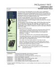
RS-485 Digital I/O Module Model 485SDD16 Document ation Number 485SDD16-1005 pn#3605-r1 This product Designed and Manufactured In Ottawa, Illinois USA of domestic and imported parts by B&B Electronics Mfg. Co. Inc. 707 Dayton Road -- P.O. Box 1040 -- Ottawa, IL 61350 PH (815) 433-5100 -- FAX (815) 433-5104 Internet: http://www.bb-elec.com [email protected] [email protected] B&B Electronics -- Revised February 2005 485SDD16-1005 Manual Cover Page B&B Electronics -- 707 Dayton Road -- Ottawa, IL 61350 PH (815) 433-5100 -- FAX (815) 433-5104 Table of Contents Chapter 5 - Software.............................................. 21 Programming Techniques..................................... 21 Read I/O Lines Command ..................................................21 Read Configuration Command ...........................................22 Set Output States Command ..............................................24 Define I/O Lines Command.................................................25 Set Power-up States Command .........................................26 Set Module Address Command ..........................................27 Set Turn-around Delay Command ......................................28 Chapter 1- Introduction........................................... 1 485SDD16 Features............................................... 1 Packing List ............................................................ 2 485SDD16 Specifications ....................................... 2 I/O Lines ................................................................................2 Inputs .................................................................................2 Outputs ..............................................................................2 Power Supply ........................................................................3 Communications ...................................................................3 Size .......................................................................................3 Demonstration Program ....................................... 29 Hard Drive Installation.......... Error! Bookmark not defined. Running Demonstration Program .......................................29 APPENDIX A..........................................................A-1 ASCII Character Codes .......................................A-1 Chapter 2 - Connections ......................................... 5 Digital I/O Connections ........................................... 5 APPENDIX B..........................................................B-1 Hexadecimal/Decimal Conversions .....................B-1 Digital Inputs .........................................................................5 Digital Outputs.......................................................................5 Ground ..................................................................................5 APPENDIX C..........................................................C-1 Interface Modules for SDD16 Models..................C-1 DTB25 .................................................................C-2 DBM16 ................................................................C-3 Serial Port Connections .......................................... 6 Power Supply Connections..................................... 8 Chapter 3 - Commands ........................................... 9 Syntax .................................................................. 10 DBM16 Interfacing ............................................................C-4 Inputs .............................................................................C-5 Outputs ..........................................................................C-7 DBM16 Specifications .......................................................C-8 I/O Lines ........................................................................C-8 Inputs .........................................................................C-8 Outputs ......................................................................C-8 Power Supply ................................................................C-8 Size................................................................................C-8 I/O Data Bytes.....................................................................10 Read I/O Lines Command .................................... 12 Set Output Lines Command ................................. 12 Set Module Address Command............................ 13 Set Turn-around Delay Command........................ 13 Define I/O Lines Command .................................. 14 Set Power-up States Command ........................... 15 Read Configuration Command ............................. 15 Appendix D Adding Data Field Confirmation.........................D-1 Chapter 4 - I/O Interfacing..................................... 17 Digital Inputs......................................................... 17 Digital Outputs ...................................................... 19 485SDD16-1005 Manual Table of Contents B&B Electronics -- 707 Dayton Road -- Ottawa, IL 61350 PH (815) 433-5100 -- FAX (815) 433-5104 i ii Table of Contents 485SDD16-1005 Manual B&B Electronics -- 707 Dayton Road -- Ottawa, IL 61350 PH (815) 433-5100 -- FAX (815) 433-5104 Chapter 1- Introduction 485SDD16 Features The 485SDD16 is a general purpose control module that operates through an RS-485 interface. The 485SDD16 offers 16 discrete digital I/O lines. With these features, the module can be used to sense external ON/OFF conditions and to control a variety of devices. Each of the sixteen I/O lines can be defined as either an input or an output. The digital outputs are CMOS compatible. The digital inputs are CMOS/TTL compatible. The digital I/O lines are available through a DB-25S (female) connector. The 485SDD16 connects to the host computer’s RS-485 or RS422 serial port using terminal blocks. The address and turn-around delay are software programmable to allow for use of multiple devices or connection to existing multi-node systems. The unit automatically detects baud rates from 1200 to 9600. A data format of 8 data bits, 1 stop bit and no parity is used. Configuration parameters are stored in non-volatile memory. These parameters consists of module address, communication turnaround delay, I/O definitions, and output power-up states. The unit is powered by connecting +12Vdc to terminal blocks or to the DB-25S I/O connector. Figure 1.2 - Simplified Block Diagram Packing List Examine the shipping carton and contents for physical damage. The following items should be in the shipping carton: 1. 485SDD16 unit 2. Software 3. This instruction manual If any of these items are damaged or missing contact B&B Electronics immediately. 485SDD16 Specifications Figure 1.1 - 485SDD16 Module 485SDD16-1005 Manual B&B Electronics -- 707 Dayton Road -- Ottawa, IL 61350 PH (815) 433-5100 -- FAX (815) 433-5104 1 I/O Lines Total: 16 (Factory default = inputs) Inputs Voltage Range: Low Voltage: High Voltage: Leakage Current: 0 Vdc to 5 Vdc 1.0 Vdc max. 2.0 Vdc min. 1 microamp max. Outputs Low Voltage: High Voltage: 0.6 Vdc @ 8.3 milliamps (Sink) 4.3 Vdc @ -3.1 milliamps (Source) 2 485SDD16-1005 Manual B&B Electronics -- 707 Dayton Road -- Ottawa, IL 61350 PH (815) 433-5100 -- FAX (815) 433-5104 Power Supply Input Voltage: Connection: 8 Vdc to 16 Vdc @ 35 milliamps (Doesn’t include the power consumption of external devices.) Terminal Blocks or DB-25S Communications Standard: Addresses: Turn-around Delay: RS-422/485 256 (Factory default = 48 decimal) Software programmable from 0 to 255 character transmission times. (Factory default = 1) Baud Rate: 1200 to 9600 (automatic detection) Format: 8 data bits, 1 stop bit, no parity Connection: Terminal Blocks Optical Isolation: If optical isolation is required, use B&B’s 485HSPR high-speed optically isolated converter with this product. Size 0.7" x 2.1" x 5.2" 485SDD16-1005 Manual B&B Electronics -- 707 Dayton Road -- Ottawa, IL 61350 PH (815) 433-5100 -- FAX (815) 433-5104 3 4 485SDD16-1005 Manual B&B Electronics -- 707 Dayton Road -- Ottawa, IL 61350 PH (815) 433-5100 -- FAX (815) 433-5104 Serial Port Connections Chapter 2 - Connections This chapter will cover the connections required for the 485SDD16. There are three sets of connections: digital I/O, serial port, and power supply. Do not make any connections to the 485SDD16 until you have read this chapter. Digital I/O Connections Connections to the I/O lines are made through the DB25S (female) I/O port connector. Refer to Table 2.1. See Chapter 5 for I/O interfacing examples. Digital Inputs The digital input lines are CMOS/TTL compatible and can handle voltages from 0Vdc to +5Vdc. Digital Outputs The digital output lines have a maximum voltage of +5Vdc and are CMOS compatible. Ground This pin should be connected to the external digital devices ground. In order to communicate to the 485SDD16 module it must be connected to an RS-422/RS-485 serial port. The 485SDD16 will work on a 2-wire or 4-wire RS-485 multi-node network. Refer to B&B Electronics’ free RS-422/485 Application Note for more information. The unit automatically detects baud rates from 1200 to 9600. A data format of 8 data bits, 1 stop bit and no parity is used. Connections are made using terminal blocks. Table 2.2 shows the terminal blocks and their functions. Table 2.2 - RS-485 Terminal Block Connections TB Label FR GND TD(A) TD(B) RD(A) Table 2.1 - 485SDD16 I/O Port Pinout DB-25S Pin # 1 2 3 4 5 6 7 8 9 10 11 12 13 Function No connection No connection No connection No connection No connection No connection Ground +12Vdc Input I/O #0 I/O #1 I/O #2 I/O #3 I/O #4 DB-25S Pin # 14 15 16 17 18 19 20 21 22 23 24 25 RD(B) +12V Function I/O #15 I/O #14 I/O #13 I/O #12 I/O #11 I/O #10 No connection I/O #9 I/O #8 I/O #7 I/O #6 I/O #5 485SDD16-1005 Manual B&B Electronics -- 707 Dayton Road -- Ottawa, IL 61350 PH (815) 433-5100 -- FAX (815) 433-5104 GND Signal Frame Ground Transmit Data (A) Transmit Data (B) Receive Data (A) Receive Data (B) +12 Vdc Power Ground Signal Direction at 485SDD16 Output Output Input Input Input - Notes Connection for frame ground. Connection is required. [Loop to RD(A) for 2-wire hookup] Connection is required. [Loop to RD(B) for 2-wire hookup] Connection is required. [Loop to TD(A) for 2-wire hookup] Connection is required. [Loop to TD(B) for 2-wire hookup] Connection is required. Connection for Signal GND and Power Supply GND. A typical 2-wire RS-485 connection is shown in Figure 2.3 and a typical RS-422 (or RS-485 4-wire) connection is shown in Figure 2.4. Note that the 485SDD16 data line labels use “A” and “B” designators (per EIA RS-485 Specification). However, some RS-485 equipment uses “+” and “-“ as designators. In almost all cases, the “A” line is the equivalent of the “-“ line and the “B” is the equivalent of the “+” line. With an RS-485/422 system there are other factors that require consideration, such as termination and turn-around delay. For more information refer to B&B Electronics’ free RS-422/485 Application Note. 5 6 485SDD16-1005 Manual B&B Electronics -- 707 Dayton Road -- Ottawa, IL 61350 PH (815) 433-5100 -- FAX (815) 433-5104 Figure 2.3 - RS-422 4-wire Connection Figure 2.1 - Example of Multi-Node Network Power Supply Connections 485SDD16 485SDD16 Power to the 485SDD16 must be supplied by an external power supply connected to the +12Vdc and GND terminal blocks or to the I/O connector. An external power supply must be able to supply 8 to 16 Vdc at 35ma. 485SDD16 NOTE: Power requirements of the module does not include the power consumption of any external devices connected to the module. Therefore, any current that is sourced by the digital outputs must be added to this value and the current must not exceed the maximum output source current. Refer to the 485SDD16 Specification Section of Chapter 1. Figure 2.2 - RS-485 2-wire Connection 485SDD16-1005 Manual B&B Electronics -- 707 Dayton Road -- Ottawa, IL 61350 PH (815) 433-5100 -- FAX (815) 433-5104 7 8 485SDD16-1005 Manual B&B Electronics -- 707 Dayton Road -- Ottawa, IL 61350 PH (815) 433-5100 -- FAX (815) 433-5104 Table 3.2 - Equivalent Values Chapter 3 - Commands There are only two commands required to control the 485SDD16: set output lines, and read I/O lines. Five additional commands are used for configuring the module: set module address, set turnaround delay, define I/O lines, set power-up states, and read configuration. Command strings are from four to six bytes in length: the “!” character, an address byte, two command characters, and one or two data bytes (if required). (See Table 3.1). Table 3.1 - 485SDD16 Commands Function Read I/O Lines Set Output Lines Set Module Address Set Turn-around Delay Define I/O Lines Set Power-up States Read Configuration Command Response !{addr}RD !{addr}SO{I/O msb}{I/O lsb} !{addr}SA{new adr} !{addr}SC{#} {I/O msb}{I/O lsb} no response Hexadecimal ! 0 A C D O R S 33 48 65 67 68 79 82 83 21h 30h 41h 43h 44h 4Fh 52h 53h Command strings consist of four to six bytes. The first byte is the start of message byte. The start of message byte is always the ASCII “!” character. The second byte is the address byte. This byte allows each unit to have a unique address. The factory default address is the ASCII "0" character. The next two bytes are the command characters. These bytes are ASCII characters and used to specify which command will be executed by the module. Some commands require an argument field containing a fifth and sometimes a sixth data byte. Commands that manipulate I/O lines require two data bytes, a Most Significant and a Least Significant data byte respectively. !{addr}SD{I/O msb}{I/O lsb} no response !{addr}SS{I/O msb}{I/O lsb} no response I/O Definitions !{addr}RC {I/O msb}{I/O lsb} Power-up States {I/O msb}{I/O msb} RS-485 Config. {addr}{t-a delay} Symbols: {...} represents one byte <...> represents a numeric value Before going into the specifics of each command, it is important to understand that a byte has a numeric value from 0 to 255. The byte's value can be represented in decimal (0 - 255) format, hexadecimal (00 - FF) format, binary (00000000 - 11111111) format, or as an ASCII character. The fixed bytes of each command will be represented as ASCII characters. For example the Read I/O command contains the following ASCII characters: “!" and "RD”. Refer to Table 3.1. However, it is important to remember that an ASCII character has a numeric value. Example: the ASCII "0" (zero) does not have a numeric value of zero but has a value of 48. The decimal and hexadecimal equivalents of some ASCII characters are shown in Table 3.2. Some commands require additional data bytes to complete the command. These data bytes may be represented in any of the formats list above. Refer to Appendix A for more ASCII and decimal equivalents. B&B Electronics -- 707 Dayton Road -- Ottawa, IL 61350 PH (815) 433-5100 -- FAX (815) 433-5104 Decimal Syntax no response no response 485SDD16-1005 Manual ASCII 9 0 _ _ _ _ Command Syntax: ! | | | | | | | | | | | 6th Data Byte | | | | 5th Data Byte | | | 2nd Command Byte | | 1st Command Byte | Address Byte Start of Message Byte I/O Data Bytes When constructing commands to manipulate output lines or when reading the state of the I/O lines it is necessary to know how to select and interpret the I/O data bytes. The sixteen I/O lines are represented by two data bytes. The Most Significant data byte represents I/O lines #15 through #8 and the Least Significant data byte represents I/O lines #7 through #0. The Most Significant byte is always sent and received first followed by the Least Significant byte. 10 485SDD16-1005 Manual B&B Electronics -- 707 Dayton Road -- Ottawa, IL 61350 PH (815) 433-5100 -- FAX (815) 433-5104 Read I/O Lines Command A byte represents an eight-bit binary number (11111111), therefore each byte can represent eight I/O lines. Each bit is assigned a bit position and a weight (value). Refer to Table 3.3. The Read I/O Lines command returns two data bytes that reflect the state of the I/O lines. The first data byte contains the most significant I/O lines (15 - 8). The second data byte contains the least significant I/O lines (7 - 0). If a bit is a "0" then the state of that I/O line is LOW. If a bit is a "1" then the state of that I/O line is HIGH. Table 3.3 - Bit Assignments for I/O Lines I/O Line # Bit Position Hex Weight Dec. Weight MOST SIGNIFICANT I/O BYTE 15 14 13 12 11 10 7 6 5 4 3 2 80 40 20 10 8 4 128 64 32 16 8 4 9 1 2 2 8 0 1 1 I/O Line # Bit Position Hex Weight Dec. Weight LEAST SIGNIFICANT I/O BYTE 7 6 5 4 3 2 7 6 5 4 3 2 80 40 20 10 8 4 128 64 32 16 8 4 1 1 2 2 0 0 1 1 To set an output to a HIGH state the corresponding bit position must be set to a "1". Conversely to set an output LOW the corresponding bit position must be set to a "0". When reading I/O lines, any bit set to a "0" indicates the corresponding I/O line is in the LOW state and any bit set to a "1" indicates the corresponding I/O line is in the HIGH state. Example 3.1 - To set outputs 15, 8, 1, and 0 to a HIGH state, and all other outputs to a LOW state (shown in bold face) Shown in binary Shown in decimal Shown in hexadecimal - MS Byte 10000001 129 (128+1) 81 (80h+1h) LS Byte 00000011 3 (2+1) 3 (2h+1h) Example 3.2 - Reply from Read I/O command (shown in bold face) Shown in binary Shown in decimal Shown in hexadecimal - MS Byte 11001000 200 (128+64+8) C8 (80h+40h+8h) LS Byte 01010010 82 (64+16+2) 52 (40h+10h+2h) I/O lines #15, 14, 11, 6, 4, 1 are HIGH and all other I/O lines are LOW. 485SDD16-1005 Manual B&B Electronics -- 707 Dayton Road -- Ottawa, IL 61350 PH (815) 433-5100 -- FAX (815) 433-5104 11 Command: !{addr}RD Argument: none Response: the state of the 16 I/O lines in two 8 bit bytes. (shown in bold face) ASCII Example: !0RDÈR Dec. Example: !0RD<200><82> Hex. Example: !0RD<C8><52> Bin. Example: !0RD<11001000><01010010> Description: Read module 0's (decimal 48) I/O lines. The first byte indicates that I/O lines #15, 14, & 11 are HIGH and I/O lines # 13, 12, 10, 9, & 8 are LOW; the second byte indicates that I/O lines # 6, 4, & 1 are HIGH and I/O lines # 7, 5, 3, 2, & 0 are LOW. Set Output Lines Command The Set Output Lines command is used to set the states of the output lines. This command requires two data bytes. These data bytes specify the output state of each output line. The first data byte represents the most significant I/O lines (15 - 8). The second data byte represents the least significant I/O lines (7 - 0). If a bit position is set to a "0" then the state of that output line will be set LOW. If a bit position is set to a "1" then the state of that output line will be set HIGH. NOTE: Refer to the "Define I/O Lines" command to define an I/O line as an output. Command: !{addr}SO Argument: {I/O msb}{I/O lsb} Response: none ASCII Example: !0SOUA Dec. Example: !0SO<85><65> Hex. Example: !0SO <55><41> Bin. Example: !0SO<01010101><01000001> Description: Set module 0's (decimal 48) output lines. The first byte sets output lines #14, 12, 10, & 8 HIGH and output lines #15, 13, 11, & 9 LOW; the second byte sets output lines #6, & 0 HIGH and output lines # 7, 5, 4, 3, 2, & 1 LOW. Note: If any of these lines are defined as inputs the bit settings are ignored. 12 485SDD16-1005 Manual B&B Electronics -- 707 Dayton Road -- Ottawa, IL 61350 PH (815) 433-5100 -- FAX (815) 433-5104 Define I/O Lines Command Set Module Address Command The Set Module Address command is used to change the address of a 485SDD16. This commands requires one data byte. This data byte is used to specify the module's new address. Addresses can be assigned any decimal value from 0 to 255. The address is stored in non-volatile memory and is effective immediately. Each module must be assigned its own unique address when connected to an RS-485 muti-node network. Command: !{addr}SA Argument: {new address} Response: none ASCII Example: !0SA9 Dec. Example: !0SA<57> Hex. Example: !0SA<39> Bin. Example: !0SA<00111001> Description: Change module address from ASCII "0" (48 decimal) to address ASCII "9" (57 decimal). The Define I/O Lines command is used to define each of the 16 I/O lines as either an input or an output. This command requires two data bytes. Each data byte defines eight I/O lines. The first data byte defines the eight most significant I/O lines (15 - 8). The second data byte defines the eight least significant digital I/O lines (7 - 0). If a bit position is set to a "0" then the I/O line will defined as an input. If a bit position set to a "1" then the I/O line will be defined as an output. Command: !{addr}SD Argument: {I/O msb}{I/O lsb} Response: none ASCII Example: !0SDUA Dec. Example: !0SD<85><65> Hex. Example: !0SD<55><41> Bin. Example: !0SD<01010101><01000001> Description: Define module 0's (decimal 48) I/O lines. The first byte define I/O lines #14, 12, 10, & 8 as outputs and I/O lines #15, 13, 11, & 9 as inputs; the second byte define I/O lines #6, & 0 as outputs and I/O lines #7, 5, 4, 3, 2, & 1 as inputs. Set Turn-around Delay Command The Set Turn-around Delay command sets the amount of time the 485SDD16 waits before transmitting its response. This ensures that no two drivers are enabled at the same time on a two-wire RS485 network. The turn-around delay is stored in non-volatile memory. This command requires a data byte that specifies the turnaround delay. Where {turn-around delay} is a number from 0 to 255. One unit of turn-around is equal to one character transmission time. The turn-around delay can be computed as follows: character time = (1 / baud rate) * 10 turn-around delay = character time * data byte Command: !{addr}SC Argument: {turn-around delay} Response: none ASCII Example: !9SC♦ Dec. Example: !9SC<04> Hex. Example: !9SC<04> Bin. Example: !9SC<00000100> Description: Set module 9's (decimal 57) turn-around delay to four character transmission times (@ 9600 baud the turn-around delay = 4.17ms). 485SDD16-1005 Manual B&B Electronics -- 707 Dayton Road -- Ottawa, IL 61350 PH (815) 433-5100 -- FAX (815) 433-5104 13 14 485SDD16-1005 Manual B&B Electronics -- 707 Dayton Road -- Ottawa, IL 61350 PH (815) 433-5100 -- FAX (815) 433-5104 Set Power-up States Command The Set Power-up States command is used to set the states of output lines when the module's power is recycled. This command requires two data bytes. These data bytes specify the output state of each output line. The first data byte represents the eight most significant I/O lines (15 - 8). The second data byte represents the eight least significant I/O lines (7 - 0). If a bit position is set to a "0" then the state of that output line will be set LOW. If a bit position is set to a "1" then the state of that output line will be set HIGH. Command: !{addr}SS Argument: {I/O msb}{I/O lsb} Response: none ASCII Example: !0SSÛ@ Dec. Example: !0SS<219><64> Hex. Example: !0SS<DB><40> Bin. Example: !0SS<11011011><01000000> Description: Set module 0's (decimal 48) power-up states. The first byte sets output lines #15, 14, 12, 11, 9, & 8 HIGH and output lines #13, & 10 LOW at power-up; the second byte sets output line #6 HIGH and output lines #7, 5, 4, 3, 2, 1, & 0 LOW at power-up. NOTE: If any of these lines are defined as inputs the bit settings are ignored. ASCII Example: !9RCUAP@9♦ Dec. Example: !9RC<85><65><80><64><57><04> Hex. Example: !9RC<55><41><50><40><39><04> Bin. Example: !0RC<01010101><01000001><01010000><01000000> <00111001><00000100> Description: Read module 9's (decimal 57) configuration. The first byte (MSB of I/O definitions) - I/O lines #14, 12, 10, & 8 are outputs and I/O lines #15, 13, 11, & 9 are inputs; the second byte (LSB of I/O definitions) - I/O lines #6, & 0 are outputs and I/O lines #7, 5, 4, 3, 2, & 1 are inputs; the third byte (MSB of output power-up states) output lines #14, & 12 HIGH and output lines #10, & 8 LOW at power-up; the fourth byte (LSB of output power-up states) - output line #6 HIGH and output line #0 LOW at power-up; the fifth byte (module address) is set ASCII "9" (decimal 57); the sixth byte (turnaround delay) is a decimal 4. Read Configuration Command The Read Configuration command returns the module's I/O definitions, the outputs power-up state, the module's address, and the turn-around delay. Six data bytes are returned. The first two data bytes contain the definition of the eight most significant I/O lines (15 - 8) and the eight least significant I/O lines (7 - 0) respectively. If a bit position is set to a "0" the I/O line is defined as an input, if set to a "1" the I/O line is defined as an output. The second two data bytes contain the power-up states of the most significant output lines (15 8) and the least significant output lines (7 - 0) respectively. If a bit position is set to a "0" the power-up state of the output will be LOW, if set to a "1" the output will be HIGH. The fifth data byte is the module's address. The sixth data byte is the turn-around delay. Command: !{addr}RC Argument: none Response: definition of the sixteen I/O lines in two 8 bit bytes, and the power-up states in two 8 bit bytes. (shown in bold face) 485SDD16-1005 Manual B&B Electronics -- 707 Dayton Road -- Ottawa, IL 61350 PH (815) 433-5100 -- FAX (815) 433-5104 15 16 485SDD16-1005 Manual B&B Electronics -- 707 Dayton Road -- Ottawa, IL 61350 PH (815) 433-5100 -- FAX (815) 433-5104 Chapter 4 - I/O Interfacing This chapter will explain "HIGH" and "LOW" states and show some general examples of how to interface to the I/O lines. Caution must be taken not to exceed 485SDD16 specifications listed in Chapter 1 when interfacing to external devices. Failure to stay within these specifications could result in damage to the unit and will void warranty. Digital Inputs As stated earlier, digital input lines are CMOS/TTL compatible and can only handle voltages from 0Vdc to +5Vdc. Digital inputs are used to sense a HIGH or a LOW state. This can be accomplished via switch closures, contact closures, or a solid state digital signal. When an I/O line, defined as an input, senses a voltage level above +2.0Vdc it will be considered "HIGH" and it's input state will be read as a "1". Conversely, when an input senses a voltage level below +1.0Vdc it will be considered "LOW" and it's input state will be read as a "0". Inputs can also be used to sense AC voltages by using mechanical or solid state relays. Solid state relays are available from many manufacturers. Figures 4.1 - 4.4 show examples of some typical input interfaces. Figure 4.2 - Solid State Input Figure 4.3 - Isolated Mechanical Input Figure 4.1 - Switch Input 485SDD16-1005 Manual B&B Electronics -- 707 Dayton Road -- Ottawa, IL 61350 PH (815) 433-5100 -- FAX (815) 433-5104 17 18 485SDD16-1005 Manual B&B Electronics -- 707 Dayton Road -- Ottawa, IL 61350 PH (815) 433-5100 -- FAX (815) 433-5104 Figure 4.4 - Isolated Solid State Input Figure 4.6 - Isolated Solid State Output Digital Outputs Digital outputs are used to turn on or turn off external devices. Digital outputs are CMOS compatible and operate between 0Vdc and +5Vdc. Outputs can be used to control solid state output modules, CMOS and TTL logic circuits. Caution must be taken not to exceed the power capability of the outputs. Refer to the output specifications in Chapter 1. Setting an output line to a "1" forces the output HIGH, and setting an output line to a "0" forces the output LOW. Figures 4.5 - 4.6 show examples of some typical output interfaces. Figure 4.5 - Solid State Output 485SDD16-1005 Manual B&B Electronics -- 707 Dayton Road -- Ottawa, IL 61350 PH (815) 433-5100 -- FAX (815) 433-5104 19 20 485SDD16-1005 Manual B&B Electronics -- 707 Dayton Road -- Ottawa, IL 61350 PH (815) 433-5100 -- FAX (815) 433-5104 Chapter 5 - Software This chapter will be divided into two sections. The first section covers programming techniques for constructing a command string, receiving data and manipulating data in QuickBASIC. The second section discusses how to install and run the demonstration program on an IBM PC or compatible. Programming Techniques This section shows steps and examples of programming the 485SDD16 in QuickBasic. If you are programming in another language, this section can be helpful as a guideline for programming the 485SDD16. Read I/O Lines Command The Read I/O Lines command returns two data bytes that represents the states of the module's I/O lines. Refer to this command in Chapter 3 for more information. Step 1 - Constructing the command string: Cmnd$ = "!" + CHR$(Maddr) + "RD" Where Maddr is the address of the module that is to return its I/O states. Step 2 - Transmitting the command string: PRINT #1, Cmnd$; Step 3 - Receiving the data: MSIO$ = INPUT$(1,#1) LSIO$ = INPUT$(1,#1) Step 4 - Manipulating the data: MSIO = ASC(MSIO$) LSIO = ASC(LSIO$) Step 5 - Determining an I/O's status: MSstatus = MSIO AND mask LSstatus = LSIO AND mask By "ANDing" the value of MSIO or LSIO with the appropriate mask of an I/O line, the status of the I/O line can be determined. If the status is equal to zero the I/O line is LOW. If the status is not equal to zero the I/O line is HIGH. Table 5.1 shows the mask values for each I/O line. Step 6 - Repeat Step 5 until the status of each I/O line has been determined. 485SDD16-1005 Manual B&B Electronics -- 707 Dayton Road -- Ottawa, IL 61350 PH (815) 433-5100 -- FAX (815) 433-5104 21 Example 5.1 - Determining the status of I/O lines #2 & #10 of module #5. Maddr = 5 mask = &H4 Cmnd$ = "!" + CHR$(Maddr) + "RD" PRINT #1, Cmnd$; MSIO$ = INPUT$(1,#1) LSIO$ = INPUT$(1,#1) MSIO = ASC(MSIO$) LSIO = ASC(LSIO$) MSstatus = MSIO AND mask LSstatus = LSIO AND mask If LSstatus equals zero then I/O line #2 is LOW. If LSstatus is not equal to zero then I/O line #2 is HIGH. If MSstatus equals zero then I/O line #10 is LOW. If MSstatus is not equal to zero then I/O line #10 is HIGH. Table 5.1 - Digital I/O Mask Values I/O Line # 0&8 1&9 2 & 10 3 & 11 4 & 12 5 & 13 6 & 14 7 & 15 Mask Values Hexadecimal Decimal 1H 2H 4H 8H 10H 20H 40H 80H 1 2 4 8 16 32 64 128 Read Configuration Command The Read Configuration command reads the module's I/O definitions, Power-up states, Address, and Turn-around delay respectively. Refer to this command in Chapter 3 for more information. Step 1 - Constructing the command string: Cmnd$ = "!" + CHR$(Maddr) + "RC" Where Maddr is the address of the module that is to return its configuration. Step 2 - Transmitting the command string: PRINT #1, Cmnd$; 22 485SDD16-1005 Manual B&B Electronics -- 707 Dayton Road -- Ottawa, IL 61350 PH (815) 433-5100 -- FAX (815) 433-5104 Step 3 - Receiving the data: MSdefs$ = INPUT$(1,#1) LSdefs$ = INPUT$(1,#1) MSpups$ = INPUT$(1,#1) LSpups$ = INPUT$(1,#1) Maddr$ = INPUT$(1,#1) Mtdly$ = INPUT$(1,#1) Step 4 - Manipulating the data: MSdefs = ASC(MSdefs$) LSdefs = ASC(LSdefs$) MSpups = ASC(MSpups$) LSpups = ASC(LSpups$) Maddr = ASC(Maddr$) Mtdly = ASC(Mtdly$) Step 5 - Determining the I/O line definitions: MSdefs = MSdefs AND mask LSdefs = LSdefs AND mask By "ANDing" the value of MSdefs or LSdefs with the appropriate mask of an I/O line, the I/O line definition can be determined. If the status is equal to zero the I/O line is an INPUT. If the status is not equal to zero the I/O line is an OUTPUT. Table 5.1 shows the mask values for each I/O line. Step 6 - Repeat Step 5 until the status of each I/O line has been determined. Step 7 - Determining an OUTPUT's Power-up state: MSpups = MSpups AND mask LSpups = LSpups AND mask By "ANDing" the value of MSpups or LSpups with the appropriate mask of an Output line, the Output line definition can be determined. If the status is equal to zero the Output power-up state will be LOW. If the status is not equal to zero the Output power-up state will be HIGH. Table 5.1 shows the mask values for each I/O line. Step 8 - Repeat Step 7 until the power-up state of each Output line has been determined. Maddr = 5 mask = &H4 Cmnd$ = "!" + CHR$(Maddr) + "RC" PRINT #1, Cmnd$; MSdefs$ = INPUT$(1,#1) LSdefs$ = INPUT$(1,#1) MSpups$ = INPUT$(1,#1) LSpups$ = INPUT$(1,#1) Maddr$ = INPUT$(1,#1) Mtdly$ = INPUT$(1,#1) MSdefs = ASC(MSdefs$) LSdefs = ASC(LSdefs$) MSpups = ASC(MSpups$) LSpups = ASC(LSpups$) Maddr = ASC(Maddr$) Mtdly = ASC(Mtdly$) MSdefs = MSdefs AND mask LSdefs = LSdefs AND mask MSpups = MSpups AND mask LSpups = LSpups AND mask If LSdefs equals zero then I/O line #2 is an INPUT and if not equal to zero then I/O line #2 is an OUTPUT. If MSdefs equals zero then I/O line #10 is an INPUT and if not equal to zero then I/O line #10 is an OUTPUT. If LSpups equals zero then Output line #2's power-up state is LOW and if not equal to zero then Output line #2's power-up state is HIGH. If MSpups equals zero then Output line #10's powerup state is LOW and if not equal to zero then Output line #10's power-up state is HIGH. Maddr is the decimal address of the module. Mtdly is the decimal number of character times that make up the turn-around delay. Example 5.2 - Determining the definition and power-up state of I/O lines #2 & #10 of module #5. Set Output States Command The Set Output States command is used to set the states of any I/O line that is defined as an output. This command requires two data bytes. Refer to this command in Chapter 3 for more information. Step 1a - Construct the command string: Set appropriate outputs HIGH MSstates = MSstates OR mask LSstates = LSstates OR mask By "ORing" the current states with the appropriate mask of a digital output line, the output's bit will be set to a "1" (HIGH). 485SDD16-1005 Manual 24 B&B Electronics -- 707 Dayton Road -- Ottawa, IL 61350 PH (815) 433-5100 -- FAX (815) 433-5104 23 485SDD16-1005 Manual B&B Electronics -- 707 Dayton Road -- Ottawa, IL 61350 PH (815) 433-5100 -- FAX (815) 433-5104 Step 1b - Set appropriate outputs LOW MSstates = MSstates AND (NOT(mask)) LSstates = LSstates AND (NOT(mask)) By "ANDing" the current states with the complement of the appropriate mask of a digital output line, the output's bit will be set to a "0" (LOW). Step 1c - Completing the command string: Cmnd$ = "!" + CHR$(Maddr) + "SO" + CHR$(MSstates) + CHR$(LSstates) Step 2 - Transmitting the command string: Print #1, Cmnd$; Example 5.3 - Set Output #0 HIGH and Output #14 LOW of module #5. 'Set module address. Maddr = 5 'Set bit 0 of LSstates to make Output #0 HIGH. LSstates = LSstates OR &H1 'Clear bit 4 of MSstates to make Output #14 LOW. MSstates = MSstates AND (NOT(&H40)) Cmnd$ = "!" + CHR$(Maddr) + "SO" + CHR$(MSstates) + CHR$(LSstates) PRINT #1, Cmnd$; Output #0 will be set HIGH and output #14 will be set LOW of module #5. All other output settings of module #5 will not be changed. Define I/O Lines Command The Define I/O Lines command is used to define each of the module's I/O lines as either an input or an output. This command requires two data bytes. Refer to this command in Chapter 3 for more information. Step 1a - Construct the command string: Define an I/O line as Output MSdefs = MSdefs OR mask LSdefs = LSdefs OR mask By "ORing" the current definitions with the appropriate I/O line mask, the I/O line's data bit will be set to a "1" (HIGH) and the I/O line will be defined as an Output. 485SDD16-1005 Manual B&B Electronics -- 707 Dayton Road -- Ottawa, IL 61350 PH (815) 433-5100 -- FAX (815) 433-5104 25 Step 1b - Define an I/O line as an Input MSdefs = MSdefs AND (NOT(mask)) LSdefs = LSdefs AND (NOT(mask)) By "ANDing" the current definitions with the complement of the appropriate I/O line mask the I/O line's data bit will be set to a "0" (LOW) and the I/O line will be defined as an Input. Step 1c - Completing the command string: Cmnd$ = "!" + CHR$(Maddr) + "SD" + CHR$(MSdefs) + CHR$(LSdefs) Step 2 - Transmitting the command string: Print #1, Cmnd$; Example 5.4 - Define I/O line #7 as an Output (HIGH) and I/O line #8 as an input (LOW) on module #4. 'Set module's address to 4. Maddr = 4 'Set bit 7 of LSdefs to make I/O line #7 an Output (HIGH). LSdefs = LSdefs OR &H80 'Clear bit 0 of MSdefs to make I/O line #8 an Input (LOW). MSdefs = MSdefs AND (NOT(&H1)) Cmnd$ = "!" + CHR$(Maddr) + "SD" + CHR$(MSdefs) + CHR$(LSdefs) PRINT #1, Cmnd$; MSIO$ = INPUT$(1,#1) I/O #7 will be defined as an Output (HIGH) and I/O line #8 will be defined as an Input (LOW) of module #4. All other I/O definitions will not be changed. Set Power-up States Command The Set Power-up States command is used to set the states of the digital outputs at power-up. This command requires two data bytes. Refer to this command in Chapter 3 for more information. Step 1a - Construct the command string: Set appropriate outputs power-up states HIGH MSpups = MSpups OR mask LSpups = LSpups OR mask By "ORing" the current power-up states with the appropriate mask of a digital output line, the power-up state's data bit will be set to a "1" (HIGH). 26 485SDD16-1005 Manual B&B Electronics -- 707 Dayton Road -- Ottawa, IL 61350 PH (815) 433-5100 -- FAX (815) 433-5104 Step 1b - Set appropriate outputs power-up states LOW MSpups = MSpups AND (NOT(mask)) LSpups = LSpups AND (NOT(mask)) By "ANDing" the current power-up states with the complement of the appropriate mask of a digital output line, the power-up state's data bit will be set to a "0" (LOW). Step 1c - Completing the command string: Cmnd$ = "!" + CHR$(Maddr) + "SS" + CHR$(MSpups) + CHR$(LSpups) Step 2 - Transmitting the command string: Print #1, Cmnd$; Example 5.5 - Set Output #5's power-up state HIGH and Output #13's power-up state LOW on module #4. 'Set module address to 4. Maddr = 4 'Set bit 0 of LSpups to make Output #5's power-up state HIGH. LSpups = LSpups OR &H20 'Clear bit 4 of MSpups to make Output #13's power-up state LOW. MSpups = MSpups AND (NOT(&H20)) Cmnd$ = "!" + CHR$(Maddr) + "SS" + CHR$(MSpups) + CHR$(LSpups) PRINT #1, Cmnd$; MSIO$ = INPUT$(1,#1) Module's #4 output line #5's power-up state will be set HIGH and output line #13's power-up state will be set LOW. All other output power-up states will not be changed. Example 5.6 - Change the address of module with a current address of 4 decimal to the new address of 5 decimal. Maddr = 4 Naddr = 5 Cmnd$ = "!" + CHR$(Maddr) + "SA" + CHR$(Naddr) Print #1, Cmnd$; Set Turn-around Delay Command The Set Turn-around Delay command is used to set the amount of time the module will wait after receiving a command before it sends the response message. This ensures that no two communication drivers will be enabled at the same time, and is necessary when multiple modules share the same communication lines. The command requires one data byte to specify the turnaround delay. Refer to this command in Chapter 3 for more information. Step 1 - Construct the command string: Cmnd$ = "!" + CHR$(Maddr) + "SC" + CHR$(Ntdly) Where Maddr if the module's address and Ntdly is the module's new turn-around delay. Step 2 - Transmitting the command string: Print #1, Cmnd$; Example 5.7 - Set the turn-around delay of module #5 to 10 character times. Maddr = 5 Ntdly = 10 Cmnd$ = "!" + CHR$(Maddr) + "SC" + CHR$(Naddr) Print #1, Cmnd$; Set Module Address Command The Set Module Address command is used to change the address of the 485SDD16. This command requires a data byte. The data byte is used to specify the new address of the module. Step 1 - Construct the command string: Cmnd$ = "!" + CHR$(Maddr) + "SA" + CHR$(Naddr) Where Maddr if the module's current address and Naddr is the module's new address. Step 2 - Transmitting the command string: Print #1, Cmnd$; 485SDD16-1005 Manual B&B Electronics -- 707 Dayton Road -- Ottawa, IL 61350 PH (815) 433-5100 -- FAX (815) 433-5104 27 28 485SDD16-1005 Manual B&B Electronics -- 707 Dayton Road -- Ottawa, IL 61350 PH (815) 433-5100 -- FAX (815) 433-5104 Demonstration Program The 485SDD16 Demonstration (SDD16) Program (IBM PC or Compatible) provides the user with examples of how to receive and transmit commands to the 485SDD16. The SDD16.EXE is the executable program, the SDD16.BAS file is the source code in QuickBASIC. The source code provides an illustration of how to send and receive commands from the 485SDD16. NOTE: This is a demonstration program only and not intended for system applications. Running Demonstration Program Before you can run the demonstration program you must run the install program in the Hard Drive Installation section. If you are running Windows, exit Windows to DOS. To run the program follow these steps from the DOS prompt: 1. Type CD \485SDD16 and press the <Enter> key. 2. Type SDD16 and press the <Enter> key. 485SDD16-1005 Manual B&B Electronics -- 707 Dayton Road -- Ottawa, IL 61350 PH (815) 433-5100 -- FAX (815) 433-5104 29 30 485SDD16-1005 Manual B&B Electronics -- 707 Dayton Road -- Ottawa, IL 61350 PH (815) 433-5100 -- FAX (815) 433-5104 Decimal ASCII 0 ................... NUL 1 ................... SOH 2 ................... STX 3 ................... ETX 4 ................... EOT 5 ................... ENQ 6 ................... ACK 7 ................... BEL 8 ................... BS 9 ................... HT 10 ................. LF 11 ................. VT 12 ................. FF 13 ................. CR 14 ................. SO 15 ................. SI 16 ................. DLE 17 ................. DC1 18 ................. DC2 19 ................. DC3 20 ................. DC4 21 ................. NAK 22 ................. SYN 23 ................. ETB 24 ................. CAN 25 ................. EM 26 ................. SUB 27 ................. ESC 28 ................. FS 29 ................. GS 30 ................. RS 31 ................. US 32 ................. SP 33 ................. ! 34 ................. " 35 ................. # 36 ................. $ 37 ................. % 38 ................. & APPENDIX A ASCII Character Codes 485SDD16-1005 Manual Appendix A B&B Electronics -- 707 Dayton Road -- Ottawa, IL 61350 PH (815) 433-5100 -- FAX (815) 433-5104 A-1 A-2 Appendix A Decimal ............ASCII 39 .................. " 40 .................. ( 41 .................. ) 42 .................. * 43 .................. + 44 .................. " 45 .................. 46 .................. . 47 .................. / 48 .................. 0 49 .................. 1 50 .................. 2 51 .................. 3 52 .................. 4 53 .................. 5 54 .................. 6 57 .................. 9 58 .................. : 59 .................. ; 60 .................. < 61 .................. = 62 .................. > 63 .................. ? 64 .................. @ 65 .................. A 66 .................. B 67 .................. C 68 .................. D 69 .................. E 70 .................. F 71 .................. G 72 .................. H 73 .................. I 74 .................. J 75 .................. K 76 .................. L 77 .................. M 78 .................. N 79 .................. O 485SDD16-1005 Manual B&B Electronics -- 707 Dayton Road -- Ottawa, IL 61350 PH (815) 433-5100 -- FAX (815) 433-5104 Decimal............ ASCII 80 ................. P 81 ................. Q 82 ................. R 83 ................. S 84 ................. T 85 ................. U 86 ................. V 87 ................. W 88 ................. X 89 ................. Y 90 ................. Z 91 ................. [ 92 ................. \ 93 ................. ] 94 ................. ^ 95 ................. _ 96 ................. ' 97 ................. a 98 ................. b 99 ................. c 100 ............... d 101 ............... e 102 ............... f 103 ............... g 104 ............... h 105 ............... i 106 ............... j 107 ............... k 108 ............... l 109 ............... m 110 ............... n 111 ............... o 112 ............... p 113 ............... q 114 ............... r 115 ............... s 116 ............... t 117 ............... u 118 ............... v 485SDD16-1005 Manual Decimal ...........ASCII 119 ................ w 120 ................ x 121 ................ y 122 ................ z 123 ................ { 124 ................ | 125 ................ } 126 ................ ~ 127 ................ DEL 128 ................ 129 ................ 130 ................ • ................. • ................. • ................. 255 ................ Appendix A B&B Electronics -- 707 Dayton Road -- Ottawa, IL 61350 PH (815) 433-5100 -- FAX (815) 433-5104 A-3 A-4 Appendix A 485SDD16-1005 Manual B&B Electronics -- 707 Dayton Road -- Ottawa, IL 61350 PH (815) 433-5100 -- FAX (815) 433-5104 The decimal (base 10) numbering system represents each position in successive powers of 10, with each decimal symbol having a value from 0 to 9. The hexadecimal (base 16) numbering system represents each position in successive powers of 16 with each hex symbol having a value of 0 to 15. Since each hex position must have a single symbol, the symbols "A" through "F" are assigned to values 10 through 15 respectively. Refer to Table 1. The information and examples to follow will explain how to convert from a decimal number to a hexadecimal number and vice versa. Table 1. Decimal Value 0 1 2 3 4 5 6 7 8 9 10 11 12 13 14 15 APPENDIX B Hexadecimal/Decimal Conversions 485SDD16-1005 Manual Appendix B B&B Electronics -- 707 Dayton Road -- Ottawa, IL 61350 PH (815) 433-5100 -- FAX (815) 433-5104 B-1 B-2 Appendix B Hexadecimal Symbol 0 1 2 3 4 5 6 7 8 9 A B C D E F 485SDD16-1005 Manual B&B Electronics -- 707 Dayton Road -- Ottawa, IL 61350 PH (815) 433-5100 -- FAX (815) 433-5104 Hexadecimal to Decimal Conversion: Decimal = (1st Hex digit x 4096) + (2nd Hex digit x 256) + (3rd Hex digit x 16) + (4th Hex digit) Each "Hex digit" is the decimal equivalent value of the hexadecimal symbol. Example: Convert 10FC hexadecimal to decimal. 1 x 4096 = 4096 0 x 256 = 0 15 x 16 = 240 12 x 1 = 12 4348 10FC hex equals 4348 decimal. Decimal to Hexadecimal Conversion: Example: Convert 4348 decimal to hexadecimal. 4096 4348 = 1 = 1 (1st Hex digit) 4096 256 252 = 0 = 0 (2nd Hex digit) 0 16 252 = 15 = F (3rd Hex digit) 240 1 12 = 12 = C (4th Hex digit) 12 0 4348 decimal equals 10FC hexadecimal. 485SDD16-1005 Manual Appendix B B&B Electronics -- 707 Dayton Road -- Ottawa, IL 61350 PH (815) 433-5100 -- FAX (815) 433-5104 B-3 B-4 Appendix B 485SDD16-1005 Manual B&B Electronics -- 707 Dayton Road -- Ottawa, IL 61350 PH (815) 433-5100 -- FAX (815) 433-5104 DTB25 The DTB25 connects to the SDD16 models to provide easy access to the available I/O lines. The DTB25 plugs directly into the SDD16's DB25S I/O port connector. Each of the twenty-five pins on the connector is brought out to a terminal block. Refer to Table C.1. Dimensions: 0.5" x 2.1" x 4.3". An enclosure for the DTB25 is available. APPENDIX C Interface Modules for SDD16 Models Figure C.1 - DTB25 Outline Drawing Before connecting any external devices to the DTB25 make sure the SDD16 module has been properly configured (I/O lines defined, power-up states set). This will avoid possible damage to the module and to the external devices. Make sure not to exceed the voltage and current limits of the SDD16 module, failure to do so could result in damage to the module and will void the warranty. Refer to the Specification Section of this Manual. 485SDD16-1005 Manual Appendix C B&B Electronics -- 707 Dayton Road -- Ottawa, IL 61350 PH (815) 433-5100 -- FAX (815) 433-5104 C-1 C-2 Appendix C 485SDD16-1005 Manual B&B Electronics -- 707 Dayton Road -- Ottawa, IL 61350 PH (815) 433-5100 -- FAX (815) 433-5104 Table C.2 - DBM16 I/O Connections Table C.1 - DTB25 Connections DB-25P Pin # 1 2 3 4 5 6 7 8 9 10 11 12 13 Function T.B. # DB-25P Pin # Function T.B. # Unused. Unused. Unused. Unused. Unused. Unused. Ground +12Vdc Input I/O #0 I/O #1 I/O #2 I/O #3 I/O #4 1 2 3 4 5 6 7 8 9 10 11 12 13 14 15 16 17 18 19 20 21 22 23 24 25 I/O #15 I/O #14 I/O #13 I/O #12 I/O #11 I/O #10 Unused. I/O #9 I/O #8 I/O #7 I/O #6 I/O #5 14 15 16 17 18 19 20 21 22 23 24 25 T.B.1 Label I/O7 GND I/O6 I/O5 GND I/O4 I/O3 GND I/O2 I/O1 GND I/O0 GND +12 ITS DBM16 The DBM16 module provides buffering and increased power handling for all the sixteen I/O lines of the SDD16 models. Each of the I/O lines can be programmed as an input or as an output by setting a jumper on the board. The DBM16 plugs directly into the SDD16's DB25S I/O Port connector. Terminal blocks are provided for all I/O line, power, and ground connections. Refer to Table C.2. An enclosure for the DBM16 is available. Function I/O Line #7 Ground I/O Line #6 I/O Line #5 Ground I/O Line #4 I/O Line #3 Ground I/O Line #2 I/O Line #1 Ground I/O Line #0 Ground +12Vdc Input Inductive-load Transient Suppression T.B.2 Label I/O8 GND I/O9 I/O10 GND I/O11 I/O12 GND I/O13 I/O14 GND I/O15 Function I/O Line #8 Ground I/O Line #9 I/O Line #10 Ground I/O LIne #11 I/O Line #12 Ground I/O LIne #13 I/O Line #14 Ground I/O LIne #15 DBM16 Interfacing This section will show some general examples of how to interface the DBM16 I/O lines to external devices. Caution must be taken not to exceed the DBM16 specifications, failure to do so could result in damage to the DBM16 and will void the warranty. Before connecting the DBM16 to the SDD16 module and connecting any external device to the DBM16 determine which I/O lines on the SDD16 module are inputs and which are outputs. Once the inputs and outputs are known, set the jumpers on the DBM16 accordingly. Refer to Figure C.2. 485SDD16-1005 Manual Appendix C B&B Electronics -- 707 Dayton Road -- Ottawa, IL 61350 PH (815) 433-5100 -- FAX (815) 433-5104 C-3 C-4 Appendix C 485SDD16-1005 Manual B&B Electronics -- 707 Dayton Road -- Ottawa, IL 61350 PH (815) 433-5100 -- FAX (815) 433-5104 Figure C.4 - Solid State Input Figure C.2 - DBM16 Outline Drawing Inputs Digital inputs are used to sense "HIGH" and "LOW" states based on voltage levels. This is accomplished via switch closures, contact closures or a solid state digital signals. Each DBM16 input is pulled up through a resistor and will be read as a logic "1" (HIGH) by the SDD16 module. When an input on the DBM16 is grounded (below +1.5Vdc), a logic "0" (LOW) will be read by the SDD16 module. Figures C.3 - C.6 show examples of some typical input interfaces. Figure C.5 - Isolated Mechanical Input Figure C.3 - Switch Input Figure C.6 - Isolated Solid State Input 485SDD16-1005 Manual Appendix C B&B Electronics -- 707 Dayton Road -- Ottawa, IL 61350 PH (815) 433-5100 -- FAX (815) 433-5104 C-5 C-6 Appendix C 485SDD16-1005 Manual B&B Electronics -- 707 Dayton Road -- Ottawa, IL 61350 PH (815) 433-5100 -- FAX (815) 433-5104 Outputs Digital outputs are used to turn "ON" or turn "OFF" external devices. Outputs can be used to control solid state output modules, logic circuits, and relays. Caution must be taken not to exceed the power capability of the outputs. Refer to the DBM16 output specifications. Setting the SDD16 module's output line to a "1" turns "ON" the DBM16's output line. Setting the SDD16 module's output line to a "0" turns "OFF" the DBM16's output driver. The DBM16 outputs are open collector current sinking drivers. Figures C.7 - C.9 show examples of some typical output interfaces. Figure C.9 - Isolated Solid State Output DBM16 Specifications I/O Lines Total: Inputs Voltage range: Low Voltage: High Voltage: Internal pull-up current: Outputs Output Voltage: Output current: Figure C.7 - Solid State Output Output leakage current: Output saturation voltage: 16 (Factory default - set to inputs) 0Vdc to +50Vdc 0Vdc to +1.5Vdc +2.5Vdc to +50Vdc 0.5 ma +50Vdc max. 350 ma max. - only 1 output on 100 ma max. - all outputs on 50 micro amp max. 1.1Vdc max. @ 100ma CAUTION: Total output power cannot exceed 2 watts for I/O's #07 and 2 watts for I/O #8-15 @ 25 degrees C. Power Supply Input Voltage: 8Vdc to 16Vdc @ 10milliamps (Doesn't include the power consumption of external devices.) Connections: Terminal Blocks Size: 0.5" x 2.1" x 4.5" Figure C.8 - Isolated Mechanical Output 485SDD16-1005 Manual Appendix C B&B Electronics -- 707 Dayton Road -- Ottawa, IL 61350 PH (815) 433-5100 -- FAX (815) 433-5104 C-7 C-8 Appendix C 485SDD16-1005 Manual B&B Electronics -- 707 Dayton Road -- Ottawa, IL 61350 PH (815) 433-5100 -- FAX (815) 433-5104 Figure C.10 - DBM16 Schematic 485SDD16-1005 Manual Appendix C B&B Electronics -- 707 Dayton Road -- Ottawa, IL 61350 PH (815) 433-5100 -- FAX (815) 433-5104 C-9 C-10 Appendix C 485SDD16-1005 Manual B&B Electronics -- 707 Dayton Road -- Ottawa, IL 61350 PH (815) 433-5100 -- FAX (815) 433-5104 With serial communications in a laboratory environment, the possibility of a communication error occurring is minimal. However, in a harsh or an industrial environment the possibility increases. A communication error occurs when a bit transmitted as a “1” is received as a “0” or vice versa. If the 485SDD16 receives a error in one or more of the first four command characters (“!0xx”), the unit will not execute the command. However, if the 485SDD16 receives an communication error on a data byte (I/O byte for Read Digital command or state byte for Set Output State command), the command will be executed since the unit has no way of knowing that there was an error. To provide the 485SDD16 with a way of detecting errors in the data fields, an additional set of commands can be used. This set of commands begins with the “#” (23h) character, instead of the “!” (21h) character. Refer to Table D-1. With these commands every data byte that is transmitted or received is followed by its complement. For example: To read I/O lines: Command syntax: #{addr}RD Response syntax: {I/O msb}{~ I/O msb}{I/O lsb} {~ I/O lsb} Where “~” is used to indicate the “complement of.” If I/O has a reading of 1, the following would be received: {00}{FF}{01}{FE} Where FFh is the complement of 0 and FEh is the complement of 1. The complement of number “x” can be calculated in QuickBasic as follows: comp = (NOT x) AND &HFF APPENDIX D Adding Data Field Comfirmation 485SDD16-1005 Manual Appendix D B&B Electronics -- 707 Dayton Road -- Ottawa, IL 61350 PH (815) 433-5100 -- FAX (815) 433-5104 D-1 D-2 Appendix D 485SDD16-1005 Manual B&B Electronics -- 707 Dayton Road -- Ottawa, IL 61350 PH (815) 433-5100 -- FAX (815) 433-5104 Table D-1 Extended Commands Function Command Response Read I/O Lines #{addr}RD Set Output Lines #{addr}SO{I/O msb}{~I/O msb}{I/O lsb}{~I/O lsb} #{addr}SA{new addr}{~new addr} #{addr}SC{x}{~x} {I/O msb}{~I/O msb}{I/O lsb}{~I/O lsb} no response Set Module Address Set Turn-around Delay Define I/O Lines Set Power-up States Read Configuration #{addr}SD{I/O msb}{~I/O msb}{I/O msb}{~I/O msb} #{addr}SS{I/O msb}{~I/O msb}{I/O lsb}{~I/O lsb} #{addr}RC no response no response no response no response {I/O msb}{~I/O msb}{I/O lsb}{~I/O lsb}{I/O powerup msb states}{~I/O powerup msb states}{I/O powerup lsb states}{~I/O powerup lsb states}{addr}{~addr}{turnaround delay}{~turn-around delay} Where “x” is the required data byte and “~” signifies the complement of the specified byte. 485SDD16-1005 Manual Appendix D B&B Electronics -- 707 Dayton Road -- Ottawa, IL 61350 PH (815) 433-5100 -- FAX (815) 433-5104 D-3 D-4 Appendix D 485SDD16-1005 Manual B&B Electronics -- 707 Dayton Road -- Ottawa, IL 61350 PH (815) 433-5100 -- FAX (815) 433-5104