1
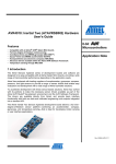
AVR1909: Display Xplained Hardware User's
Guide
Features
• 240 x 320 (QVGA) graphical TFT display
- With resistive touch
- LED Backlight
- Internal controller
• Simple SPI interface for control
• Digital (PWM) control interface for backlight
• One 40pin, 0.5mm FPC connector
• Display and backlight powered by single 3.3V
8-bit
Microcontrollers
Application Note
1 Introduction
The Display Xplained module gives the possibility to evaluate a 240 x 320 pixel
(QVGA) graphical RGB TFT display with a 4-wire touch interface and LED
backlight. The display is interfaced with a simple SPI interface to send and receive
commands and data. The Xplain kit provides tested low–level drivers and highlevel functions in order to get the developer quickly up to speed with his application
development.
Figure 1-1. Display Xplained evaluation module.
Rev. 8297A-AVR-04/10
2 Related Items
Datasheet for the LCD module (ET024006DHU) from EDT can be found here:
http://www.farnell.com/datasheets/86386.pdf
Datasheet for the graphical controller (HX8347-A) from Himax can be obtained by
contacting EDT. It may also found on the web.
Firmware for Xplain kit can be found here:
http://www.atmel.com/Xplain
Also checkout these application note:
• AVR1913: Display Xplained Firmware – Getting Started training
• AVR1921: Reprogramming the Xplain AT90USB1287 and ATxmega128A1
• AVR1922: Xplain Board Controller Firmware
3 General information
The LCD module (ET024006DHU from EDT) has a 240 x 320 pixel resolution, with up
to 6 bit pr color, giving 256k colors. The Display Xplained board uses a regular 4-wire
SPI interface to access the display. The touch interface is a 4-wire resistive touch that
should be interfaced to ADC/IO pins to work. The backlight system has three white
LEDs in parallel that can draw up to 60mA at 3.3V. For further details see the
datasheet from EDT.
Figure 3-1. Overview of the Xplain kit backside.
2
AVR1909
8297A-AVR-04/10
AVR1909
The Display Xplained module is quite simple. It basically connects the TFT display
SPI interface, resistive touch interface, and backlight interface from a 40pin FPC
connector to two female pin-headers that fit the Xplain kit.
In addition it has a program/debug interface that will connect an external
programmer/debugger to the Xplain kit through a male and a female pin-header.
3.1 The LCD Module
The LCD module is produced by EDT (Emerging Display Technologies Corp), and is
called ET024006DHU. It will be replaced with a new version called ET024008DHU in
mid 2010 that have the same outline dimension and same electronics and optical
specification.
The LCD module embeds a graphical controller/driver from Himax called HX8347-A.
This controller provides several communication interfaces like 8/16bit parallel MCU
interface, 16/18bit RGB, and 4-wire serial SPI interface. On the Display Xplained
module this has been hardwired to use serial SPI interface.
The display is attached to the PCB with a strong dual-sided foam tape adhesive that
make it easy to mount. This will electrically insulate the display from the PCB avoiding
any short-circuit problems that may be caused by vibration wearing on the solder
mask and tracks/vias. It will also provide some vibration damping for the display to
protect the glass surface from cracking. It is also quite easy to remove the display if
needed.
3.2 The Touch module
The LCD module has a 4-wire resistive touch interface. This consists of four lines (2
in each X and Y direction) that should be connected to ADC/IO pins on the MCU
interfacing it. The general procedure is to apply a voltage (VCC) for instance on the
X-lines and then measure the voltage on the Y-lines. Then the operation is repeated,
but switching the X and Y lines. This will give a (X,Y) coordinate for the touch.
In order to avoid over driving (saturate) the ADC inputs, serial resistors have been
added so the maximum voltage is within the ADC capability. This is a very simple and
low-cost solution to adjust the touch sensor output to fit the ADC inputs. It will also
lower the current consumption a little to increase the overall power performance.
For more details on how to use 4-wire resistive touch sensors, see the application
note AVR341: Four and five-wire Touch screen Controller using tinyAVR® and
megaAVR® devices
3.3 The Backlight module
The backlight module of the display consists of three white LEDs connected in
parallel. These can draw up to 60mA and have a maximum voltage drop up to 3.6V.
On the Display Xplained module the backlight is connected to the V3P3 (3.3V) powersupply. This will somewhat limit the maximum light output in change of a simpler
design.
A MOSFET turns the backlight LEDs on/off and a 4.7ohm resistor limits the maximum
current through the LEDs. This makes it quite easy to control the backlight with a
PWM signal to adjust intensity.
3
8297A-AVR-04/10
3.4 The SPI interface
The Display Xplained module uses a simple SPI interface to communicate with the
LCD module. This consist of a Chip-Select (CS) line, a clock line (SCL), and two data
lines (SDI/SDO). The SPI is operated in mode 3, i.e. inactive clock is ‘high’, and data
is latched on rising clock edge.
3.5 The SPI/USART MUX resistors
The ATxmega128A1 has swapped the MOSI and SCK signals between using the
regular SPI and using the USART in master SPI mode, which is available on the
same pins. In order to offer the possibility to use both interfaces, a simple 0-ohm
resistor mux is added to the Display Xplained module. It is currently set up to use the
USART in master SPI mode. To switch to the regular SPI mode, move the two
resistors mounted in position R111/R114 to position R112/R113.
See schematic diagram and PCB assembly drawing for details on where to find these
resistors. Note that they are placed under the LCD flexprint cable, so this needs to be
disconnected from the FPC connector to get access to the resistors Please refer to
Figure 2-1 page 2.
3.6 The LCD Tear-Enable signal (TE)
The LCD Module has an output signal that indicates when the display can be updated
without getting any tearing effects. This signal basically indicates the scan retrace
period of the display, meaning the time-period after the last pixel update and before
the first pixel is written again. This period can be used to update the graphical RAM,
and the update will be shown in the next scan period. For further details, see the
Himax HX8347-A datasheet and application notes.
3.7 The LCD Reset signal
This signal is an input to the LCD module and is used to reset it. It has a pull-up
resistor connected to avoid unintended resets. For further details, see the Himax
HX8347-A datasheet and application notes.
4 Connectors
The Display Xplained module has five 10-pin 100mil headers. Two are used for
programming/debugging interface to the Xplain kit. One is used for SPI interface and
the backlight control of the LCD module. One is used for the touch interface to the
LCD module. The last one is only used as a mechanical stabilizer to the Xplain kit.
Note that the female SMD mounted pin-headers might get damaged if not handled
carefully. The plastic insulation might come off and exposes the conductors.
The last connector on the Display Xplained module is the FPC connector for the LCD
module.
4.1 Programming headers (J103/J104)
The AVR XMEGA™ can be programmed and debugged by connecting an external
programming/debugging tool to the “JTAG & PDI XMEGA” pin header (J100). The pin
header is having a standard JTAG programmer pinout (refer to online help in AVR
Studio®), and tools like the JTAGICE mkII or the AVR ONE! can thus be connected
4
AVR1909
8297A-AVR-04/10
AVR1909
directly to the header. If it is desired to use PDI programming/debugging an adapter
or squid cable (included in the JTAGICE mkII kit) must be used. Please see Table 4-1
below for pin-out description.
Table 4-1. Programming headers (J103/J104) – JTAG and PDI.
J103/J104 pin
JTAG(1)
PDI(2)
J103/J104-1
TCK
-
J103/J104-2
GND
GND(3)
J103/J104-3
TDO
-
J103/J104-4
V3P3
V3P3(3)
J103/J104-5
TMS
-
J103/J104-6
nSRST
PDI_CLK
J103/J104-7
V3P3
V3P3(3)
J103/J104-8
-
PDI_DATA
J103/J104-9
TDI
-
J103/J104-10
GND
GND(3)
Notes:
1. Standard pin-out for JTAGICE mkII and other Atmel programming tools.
2. Requires adapter or squid cable to connect a JTAGICE mkII (refer to AVR
Studio help).
3. It is only required to connect one V3P3/GND pin.
The AT90USB1287 can be programmed by connecting a programming tool, such as
a JTAGICE mkII, to the “JTAG USB” pin header (J200) on the Xplain board. Please
refer to AVR1907: Xplain Hardware User’s Guide for details.
4.2 The resistive touch pin-header (J101)
This connector connects the resistive touch interface to AVR XMEGA’s analog
PORTA that is available on the “XMEGA PORT A” pin header on the Xplain board
(J101). This allows the user to connect external signals to the ADC, DAC and Analog
Comparators on PORTA. Please see Table 4-2 below for pin-out description
Table 4-2. The resistive touch pin-header (J101) connections.
J101 pin
LCD resistive touch signals
J101-1
-
J101-2
-
J101-3
-
J101-4
-
J101-5
TFT_XL (X-direction, Left side)
J101-6
TFT_XR (X-direction, Right side)
J101-7
TFT_YD (Y-direction, Bottom [lower] side
J101-8
TFT_YU (Y-direction, Upper side)
J101-9
GND
J101-10
-
5
8297A-AVR-04/10
4.3 The SPI/TE/Reset/backlight pin-header (J102)
This connector connects to the display’s SPI interface and backlight to the AVR
XMEGA’s digital PORTD that is available on the “AVR XMEGA PORT D” pin header
on the Xplain board(J102). Please see Table 4-3 page below for pin-out description.
Table 4-3. The SPI/TE/Reset/backlight pin-header (J102)
J102 pin
LCD SPI interface signals + backlight
J102-1
TFT_BL_PWM
J102-2
TFT_RESET
J102-3
TFT_TE (Tear-Enable signal to synchronize write)
J102-4
-
J102-5
TFT_CS
J102-6
TFT_SCL_X (Can be swapped with J102-8)
J102-7
TFT_SDO
J102-8
TFT_SDI_X (Can be swapped with J102-6)
J102-9
GND
J102-10
V3P3
4.4 The unused pin-header (J105)
This connector is not used for electrical connection on the Display Xplained module. It
is only used as mechanical stabilizing to the Xplain kit.
4.5 The LCD connector (J100)
The LCD connector is a 40-pin FPC connector with 0.5mm pitch. For details on
signal/power connections, see the schematic diagram for the Display Xplained
module.
5 Available code examples and drivers
A Getting-Started training for the Display Xplained kit can be downloaded from the
Atmel web site. The application note is called: AVR1913: Display Xplained
Firmware – Getting Started training.
Further information and drivers for Display Xplained can be downloaded as
application notes, also distributed from Atmel’s web site.
6 Mounting Display Xplained module to Xplain kit
The Display Xplained module will fit onto the expansion connectors on the Xplain kit.
Be careful to rotate the Display Xplained module correctly to the Xplain kit. The text
direction should be the same on both when rotated correctly. Also be careful to align
the connectors to avoid wrong signal/power connections that might cause damage to
the boards.
Also be careful when the Display Xplained module is removed to avoid bending pins.
Don’t use any hard tools that might cause damage to the boards. Pay attention to
EMC guidelines and proper handling precautions to avoid ESD damage to the
boards.
6
AVR1909
8297A-AVR-04/10
Disclaimer
Headquarters
International
Atmel Corporation
2325 Orchard Parkway
San Jose, CA 95131
USA
Tel: 1(408) 441-0311
Fax: 1(408) 487-2600
Atmel Asia
Unit 1-5 & 16, 19/F
BEA Tower, Millennium City 5
418 Kwun Tong Road
Kwun Tong, Kowloon
Hong Kong
Tel: (852) 2245-6100
Fax: (852) 2722-1369
Atmel Europe
Le Krebs
8, Rue Jean-Pierre Timbaud
BP 309
78054 Saint-Quentin-enYvelines Cedex
France
Tel: (33) 1-30-60-70-00
Fax: (33) 1-30-60-71-11
Atmel Japan
9F, Tonetsu Shinkawa Bldg.
1-24-8 Shinkawa
Chuo-ku, Tokyo 104-0033
Japan
Tel: (81) 3-3523-3551
Fax: (81) 3-3523-7581
Technical Support
[email protected]
Sales Contact
www.atmel.com/contacts
Product Contact
Web Site
http://www.atmel.com/
Literature Request
www.atmel.com/literature
Disclaimer: The information in this document is provided in connection with Atmel products. No license, express or implied, by estoppel or otherwise, to any
intellectual property right is granted by this document or in connection with the sale of Atmel products. EXCEPT AS SET FORTH IN ATMEL’S TERMS AND
CONDITIONS OF SALE LOCATED ON ATMEL’S WEB SITE, ATMEL ASSUMES NO LIABILITY WHATSOEVER AND DISCLAIMS ANY EXPRESS, IMPLIED
OR STATUTORY WARRANTY RELATING TO ITS PRODUCTS INCLUDING, BUT NOT LIMITED TO, THE IMPLIED WARRANTY OF MERCHANTABILITY,
FITNESS FOR A PARTICULAR PURPOSE, OR NON-INFRINGEMENT. IN NO EVENT SHALL ATMEL BE LIABLE FOR ANY DIRECT, INDIRECT,
CONSEQUENTIAL, PUNITIVE, SPECIAL OR INCIDENTAL DAMAGES (INCLUDING, WITHOUT LIMITATION, DAMAGES FOR LOSS OF PROFITS,
BUSINESS INTERRUPTION, OR LOSS OF INFORMATION) ARISING OUT OF THE USE OR INABILITY TO USE THIS DOCUMENT, EVEN IF ATMEL HAS
BEEN ADVISED OF THE POSSIBILITY OF SUCH DAMAGES. Atmel makes no representations or warranties with respect to the accuracy or completeness of the
contents of this document and reserves the right to make changes to specifications and product descriptions at any time without notice. Atmel does not make any
commitment to update the information contained herein. Unless specifically provided otherwise, Atmel products are not suitable for, and shall not be used in,
automotive applications. Atmel’s products are not intended, authorized, or warranted for use as components in applications intended to support or sustain life.
© 2010 Atmel Corporation. All rights reserved. Atmel®, Atmel logo and combinations thereof, AVR®, AVR® logo, AVR Studio®, tinyAVR®,
megaAVR® and others are the registered trademarks, XMEGATM and others are trademarks of Atmel Corporation or its subsidiaries. Other terms
and product names may be trademarks of others
8297A-AVR-04/10