1
AVR1607: Brushless DC Motor (BLDC) Control
in Sensor mode using ATxmega128A1 and
ATAVRMC323
Features
• BLDC Motor Basics
• Hardware Implementation
• Code Example
8-bit
Microcontrollers
Application Note
References
[1] ATxmega128A1 Data sheet
[2] AVR430: MC300 Hardware User Guide
[3] AVR1014: MC303 Hardware User Guide
[4] AVR601: Atmel Modular Evaluation Kits for Motor Control Applications
Glossary
BLDC : Brushless DC
PWM : Pulsed Width Modulation
IGBT : Insulated Gate Bipolar Transistor
AWEX : Advanced Waveform Extension
1 Introduction
This application note describes how to implement a control of Brushless DC motor
(BLDC) in sensor mode using the ATxmega128A1, Atmel® AVR® microcontroller
and the ATAVRMC323 development kit.
This application note deals only with BLDC motor control application using Hall
effect position sensors to control commutation sequence.
In this document, we will give a short description of brushless DC motor theory of
operations. We will detail how to control a brushless DC motor in sensor mode and
we will also provide a short description of the ATAVRMC303 and ATAVRMC300
boards used in this application note.
Software implementation is also discussed with software control loop using a PID
filter.
Rev. 8311A-AVR-07/10
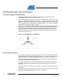
2 Brushless DC motor Theory of Operation
2.1 Simplified Model of a BLDC Motor
A simplified model of a three phases BLDC motor stator consists of three coils
arranged in three directions U, V and W (Figure 1).
A permanent magnet forms the rotor. The rotor in a BLDC motor consists of an even
number of permanent magnets. The number of magnetic poles in the rotor also
affects the step size and torque ripple of the motor. More poles provide smaller steps
and less torque ripple. The permanent magnets go from 1 to 5 pairs of poles. In
certain cases it can go up to 8 pairs of poles.
Here the rotor is outlined as a bar magnet with its rotary axis at the intersection of the
three axes U, V, W perpendicular to the plane of these axis. The orientation/position
of the permanent magnet can be controlled by driving a configuration of currents
through the three coils. The bar magnet comes to position sector 1 when a current is
driven from W through V and it comes to the following orientation (sector 2) when a
current is driven from W to U.
Figure 1. Simplified Model of a BLDC Motor
2.2 Six-step commutation
The method for energizing the motor windings in the sensor method described in this
application note is the six-step commutation. Each step, or sector, is equivalent to 60
electrical degrees. Six sectors make up 360 degrees, or one electrical revolution.
The arrows in the winding diagram Figure 2 show the direction current flows through
the motor windings in each of the six sectors.
The graph (Figure 3) shows the voltage applied at each lead of the motor during the
six sectors. Sequencing through these six sectors moves the motor one electrical
revolution.
For every sector, two windings are energized and the third winding is floating (not
energized).
Connecting the coils to the power and neutral bus induces the current flow. This is
referred to as trapezoidal commutation or block commutation.
2
AVR1607
8311A-AVR-07/10
AVR1607
Figure 2. Model of a BLDC Motor with current flows versus rotor positions
Figure 3. Commutation sequence
Notes :
- Open phase is the one shown with dotted line.
- Hall states are detailed in 2.4 section
2.3 Power Stage
The commutation pattern is controlled with a 3-phase bridge (see Figure 4). The 3
half bridges have 6 power switches (IGBT or MOSFET transistors) which are
switched according to the defined commutation pattern.
Figure 4. 3-phases bridge
3
8311A-AVR-07/10
2.4 Hall sensors
For the estimation of the rotor position, the motor is equipped with three hall sensors.
These hall sensors are placed every 120°. With these sensors, 6 different
commutations are possible. Phase commutation will depend on these hall sensor
values.
Figure 5 shows the three Hall sensors signals H1,H2,H3 as motor turns using sensor
control. Hall states are the combination result of H1,H2,H3 signals.
Figure 5. Hall states versus Motor leads in Sensor mode
With a motor of n pairs of poles, the hall sensors frequency is n times faster than the
motor rotation.
2.5 Phase Commutations
Power supply to the coils must be changed when hall sensor values change. With
right synchronized commutations, the torque remains nearly constant and high.
4
AVR1607
8311A-AVR-07/10
AVR1607
Reading hall sensors values (HS_xxx variable) indicates which new scheme should
be switched.(see following table)
Table 1-1. Switches commutation for CW rotation
Hall Sensors Value
(H1 H2 H3)
Hall
States
Previous
Phases
Previous
scheme
Next
Phases
Next
scheme
3
V-W
T3 ; T6
U-W
T1 ; T6
100
1
U-W
T1 ; T6
U-V
T1 ; T4
101
5
U-V
T1 ; T4
W-V
T5 ; T4
001
4
W-V
T5 ; T4
W-U
T5 ; T2
011
6
W-U
T5 ; T2
V-U
T3 ; T2
010
2
V-U
T3 ; T2
V-W
T3 ; T6
= HS_xxx
110
For motors with multiple poles the electrical rotation does not correspond to a
mechanical rotation. A motor with n pair of poles BLDC motor uses n electrical
rotation cycles to have one mechanical rotation.
The strength of the magnetic field determines the force and speed of the motor. By
varying the current flow through the coils, the speed and torque of the motor can be
adjusted. The most common way to control the current flow is to control the average
current flow through the coils. PWM (Pulse Width Modulation) is used to adjust the
average voltage and thereby the average current, inducing the speed. For example,
the PWM frequency selected is the range from 10kHz to 200kHz according to the
application (commutation losses, audible frequency...).
Figure 6. PWM scheme
Commutation creates a rotating field.
For instance at Step 5, Phase U is connected to the positive DC bus voltage through
T1 and Phase V is connected to ground through T4, Phase W is unpowered. Two flux
vectors are generated by phase U and phase V The sum of the two vectors creates
the stator flux vector. Then the rotor tries to follow this stator flux.
As soon as the rotor reaches the given position, the hall sensors state changes its
value from “101” to “001” a new voltage pattern is selected and applied to the BLDC
5
8311A-AVR-07/10
motor. Then Phase U is unpowered and Phase W is connected to the positive DC
bus, resulting in a new stator flux vector ‘Step 4’.
Following the commutation schematic Figure 5 and Table 1-1, we get six different
stator flux vectors corresponding to the six commutation steps. These six steps
provide one electrical revolution.
3 ATxmega128A1 microcontroller
Based on the high performance AVR 8-bit RISC architecture, the ATxmega128A1
integrates all of the basic peripherals necessary to satisfy the needs of complex
algorithms.
The ATxmega128A1 has all necessary resources to provide an integrated solution to
control BLDC motors in their system environments.
3.1 Timer/Counters
ATxmega128A1 provides 16-bit timers/counters with :
Four Compare or Capture (CC) Channels in Timer/Counter 0
Two Compare or Capture (CC) Channels in Timer/Counter 1
To generate PWM frequency, this Application Note uses three compare channels
(A,B,C) of Timer0 and the Advanced Waveform Extension (AWEX) additional feature
to Timer 0. AWEX function is available for ports C and E (Port C is used in this
Application Note).
The benefits of AWEX features for motor control are :
•
•
•
•
•
•
•
Complementary outputs from each Capture channel
Four Dead Time Insertion (DTI) which avoid cross conduction
Separate High and Low Side Dead-Time Setting
Double Buffered Dead-Time
Event Controlled Fault Protection
Single Channel Multiple Output Operation
Double Buffered Pattern Generation
The output pairs go through a Dead-Time Insertion (DTI) unit that enables generation
of the non-inverted Low Side (LS) and inverted High Side (HS) of the WG output with
dead time insertion between LS and HS switching. The DTI output will override the
normal port value according to the port override setting.
The Fault Protection unit is connected to the Event System. This enables any event to
trigger a fault condition that will disable the AWEX output. Several event channels can
be used to trigger fault on several different conditions.
3.2 Analog features
ATxmaga128A1 integrates also analog blocks like :
• Two Eight-channel, 12-bit, 2 Msps Analog to Digital Converters, with
programmable gain options.
The inputs per ADC are :
o 8 single ended inputs
6
AVR1607
8311A-AVR-07/10
AVR1607
o 8x4 differential inputs with selectable 1/2/4/8/16/32/64x gain
• Four Analog Comparators with Window compare function, with selectable
comparison levels, and interrupts on pin change I/Os.
The ATxmega128A1 includes independent positive and negative comparator inputs
available for over-current detection. The Input selection can be achieved from pins :
- Pins 0, 1, 2, 3, 4, 5, 6 for positive input
- Pins 0, 1, 3, 5, 7 for negative input
Its reference (comparison level) can be fixed via the DAC output or any external
reference voltage :
– Output from 12-bit DAC
– 64-level scaler of the VCC, available on negative analog comparator input
– Bandgap voltage reference
Refer to the ATxmega128A1 Data sheet for the complete description of the
ATxmega128A1 microcontroller.
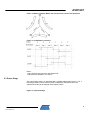
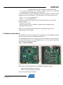
4 Hardware description
This application has been developed with ATAVRMC300 and ATAVRMC303 boards
which are the two parts of the ATAVRMC323 Starter kit..
The ATAVRMC300 board is the power board which embeds the power bridge is
connected (see below) to the ATAVRMC303 which is the processor board built
around the ATxmega128A1 processor.
Figure 7. MC303 and MC300
Please refer to the ATAVRMC300 and ATAVRMC303 Application Notes :
- AVR430: MC300 Hardware User Guide
- AVR1014: MC303 Hardware User Guide
which also provide boards schematics.
7
8311A-AVR-07/10
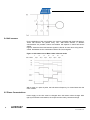
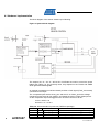
4.1 Hardware implementation
The block diagram of the sensor closed loop is following :
Figure 8. System block diagram
The outputs UH, UL, VH, VL, WH & WL of AVR303 are used to control the power
bridge (see Table 1-2). As previously seen, they depend on the Timer0 and AWEX
which generates PWM signals.
An external comparator on MC303 board provides a fault signal (Fault_overcurrent)
connected to PE4 input.:
The compared inputs are the shunt_pos and AVCC/ 34. Shunt_pos is the voltage
monitored across the 0.05 ohm resistor, and equals the motor current divided per 20.
So the comparator output will toggle as soon as motor current Im will be :
Im /20 > AVCC / 34
So limit is : Im > 2.94 A
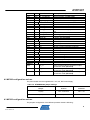
Table 1-2. Microcontroller I/O ports use (TQFP100 package)
PORT A
PA0
95
U_cond_neg
U Reference for zero-crossing (Not used)
PA1
96
V_cond_neg
V Reference for zero-crossing (Not used)
PA2
97
U_conditioned
= U / 6 (Not used)
8
AVR1607
8311A-AVR-07/10
AVR1607
PA3
PA4
PA5
PA6
PA7
PORTB
PB0
PB1
PB2
PB3
98
99
100
1
2
V_conditioned
W_conditioned
Vn_conditioned
Vm
W_cond_neg
= V / 6 (Not used)
= W / 6 (Not used)
Neutral voltage / 34 (Not used)
(Not used)
W Reference for zero-crossing (Not used)
5
6
7
8
Speed_ref
Speed Potentiometer (MC303)
Current_reference
Shunt_pos
PB4
PB5
PB6
PB7
PORTC
PC0
PC1
PC2
PC3
PC4
PC5
PORT E
PE0
PE1
PE2
PE4
PE5
PORT H
PHO
9
10
11
12
Shunt_neg
Shunt_U
Shunt_V
Shunt_W
= AVCC / 34
0.05 ohm shunt voltage ( = motor current /
20)
GND of Vmotor
= Shunt_pos (not used)
= Shunt_pos (not used)
= Shunt_pos (not used)
15
16
17
18
19
20
UL
UH
VL
VH
WL
WH
Drives T1 power transistor of MC300
Drives T2 power transistor of MC300
Drives T3 power transistor of MC300
Drives T4 power transistor of MC300
Drives T5 power transistor of MC300
Drives T6 power transistor of MC300
H1
H2
H3
Fault_overcurrent
Fault_IPM
Hall sensor 1 signal
Hall sensor 2 signal
Hall sensor 3 signal
External comparator ( MC303)output
(Not used)
ZC_U
Zero crossing external comparator output :
sensorless mode (Not used)
Zero crossing external comparator output :
sensorless mode (Not used)
Zero crossing external comparator output :
sensorless mode (Not used)
PH1
ZC_V
PH2
ZC_W
4.2 MC300 configuration and use
The power board must be supplied with a 12V, 2A, DC Power Supply.
Table 1-3. ATAVRMC300 jumper settings
Jumper
Position
Comment
J1(VHa)
Pin1 & 2 shorted
VHa = +5V
J2(VCC)
Open
Vcc = +5V
4.3 MC303 configuration and use
The jumpers configuration of the MC303 processor board is following :
9
8311A-AVR-07/10
Table 1-4. ATAVRMC303 jumper settings
Jumper
Position
Comment
J15
Open
Shunt_neg (Jumpers to be removed to
enable JTAG Programming)
J16
Open
Shunt_U (Jumpers to be removed to
enable JTAG Programming)
J17
Open
Shunt_V (Jumpers to be removed to
enable JTAG Programming)
J18
Open
Shunt_W (Jumpers to be removed to
enable JTAG Programming)
4.4 Power-supply
This firmware example has been configured according to a power-supply Vm=12V.
This power-supply must be able to provide up to 4A output current.
4.5 Motor
The BLDC motor provided inside MC323 and MC300 Motor Control Kit has the
following characteristics:
Manufacturer : TECMOTION
Number of phases : 3
Number of poles : 8 (4 pairs)
Rated voltage : 24V
Rated speed : 4000 rpm
Rated torque : 62.5 Nm
Torque constant : 35 Nm/A = k_tau
Line to Line Resistance : 1.8 ohm = R
Back EMF : 3.66 V/Krpm = k_e
Peak current : 5.4A
Maximum speed is 6900 rpm.
4.6 Technical Advices
4.6.1 Disconnecting the BLDC Motor
The BLDC motor must not be disconnected while it is running or while its coils carry
current. It is allowed to disconnect a BLDC motor if the PWM duty cycle is 0% and the
rotor is at rest so that no current is driven through the coils. Be careful, when stopping
the power supply or PWM, a BLDC motor with a high moment of inertia is able to run
for a relatively long time.
10
AVR1607
8311A-AVR-07/10
AVR1607
4.6.2 Ground and Power Wirings
One design its own board has to take care of the ground wiring and power wiring. The
power supply of the processor and additional signal conditioning components (e.g.
additional fast comparators, operational amplifiers) has to be decoupled from the
motor power supply. The ground connection has to be of low resistance and low
inductance to prevent against voltage drop and noise due to high currents. A ground
plane within a multi layer PCB is recommended for proper operation.
5 Firmware
The source file directory embeds an html documentation which can be opened
through the readme.html file.
The application to ATxmega128A1 is detailed in following sections.
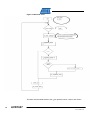
5.1 Main Flow chart
The firmware flowchart is described below :
11
8311A-AVR-07/10
Figure 9. Main flow chart
The tasks are scheduled thanks to the g_tick produced each 1.024ms with Timer1.
12
AVR1607
8311A-AVR-07/10
AVR1607
5.2 INIT : Initialisation functions
The initialization functions are following
5.2.1 clock_init()
• Oscillator : 32MHz RC oscillator and OSC oscillator
• PLL : clock source=32MHz and factor =16
• Prescalers: PSADIV=1 and PSB and PSCDIV=2 : means clk_PE R4 = 128MHz,
clk_PE R2 = 64MHz and clk_PE R= 32MHz
5.2.2 mc_init()
•
Port C : pins 0 to 5 are in output mode and clear (DIRSET and OUTCLR=1) are
the outputs connected to transistor power bridge
• Port E : The input pull up are activated to connect the Hall sensor signals
• External Interrupts are defined on Port E Pins0/1/2 (Hall signals)
• Timer 0 configuration is :
Clock prescaler /4 (8MHz)
PWM_Init (255) configures a PWM frequency = 15686 kHz
• Timer1 configuration is :
No Clock prescaler and period=8000 produces a g_tick each 1.024 ms
• ADCB configuration is :
- calibration/offset
- signed conversion mode and 12 bit resolution.
- ADC prescaler to a Sample rate of CPUFREQ/16. Allow time for storing data. */
- Set reference voltage to VCC-0.6 V
- Setup channel 0 to have single ended input and gain=1
- Set input to the channels in ADC B to be PIN 0
- Enable ADC B with free running mode
5.3 Regulation functions
The main loop functions are following.
5.3.1 mci_set_motor_speed ()
This function updates the speed setpoint according to the potentiometer adjustment
or the speed command received on serial transmission.
mc_get_potentiometer_value() returns mc_potentiometer_value
5.3.2 mc_regulation_loop() :
The duty_cycle variable controls the PWM generator. This variable is the result of
following functions :
in Open loop mode : duty_cycle = mc_get_motor_speed()
in Speed loop mode : duty_cycle = mc_control_speed(mc_get_motor_speed())
in Current loop mode :
13
8311A-AVR-07/10
duty_cycle = mc_control_current(mc_get_potentiometer_value())
5.4 Commutation
The phase commutation has to be achieved according to the 3 Hall sensors.
Commutation between steps is achieved when a rising or falling edge occurs on one
of the 3 Hall sensor signals.
Hall sensor signals H1/H2/H3 are connected to PE0/PE1/PE2 which are configured
as interrupt sources.
(Another solution could be using internal comparators to generate interrupts.)
Port Interrupt 0 Mask is defined as :
sfrb PORTE_INT0MASK = 0x068A
Are also defined :
#define PORTE_INT0MASK
PORTE.INT0MASK
PORTE.INT0MASK = (PIN0_bm | PIN1_bm | PIN2_bm);
This means that PORTE_INT0_vect (HALL-A()) is executed if any of the three Hall
senor signal is changing.
This interrupt vector executes :
• The transistor commutation according to the HALL_SENSOR_VALUE :
HALL_SENSOR_VALUE is the value of the 3 Hall sensor bits = PORTE.IN & 0x07
The commutation is achieved by the function :
mc_switch_commutation(HALL_SENSOR_VALUE)
• and estimation of speed on Rising edge of H1 (Hall A) sensor. This means the
speed is evaluated one time per electrical cycle.
5.4.1 mc_switch_commutation()
This function achieves two operations:
• First,the update of the duty-cycle, thanks to function
:mc_duty_cycle(mc_get_Duty_Cycle())
This is achieved with the update of the Output new compare value of the Timer:
TC_SetCompareA( &TCC0, level ); which updates CCABUF register with new
compare value
TC_SetCompareB( &TCC0, level );
TC_SetCompareC( &TCC0, level );
The dead time insertion is achieved with ConfigDTI() function which configures a
dead Time both sides equal to 3.
14
AVR1607
8311A-AVR-07/10
AVR1607
•
and secondly, a switch of the power bridge according to next expected position
and the direction of the rotation.
AWEX feature, described previously is configured on PortC.
Port C0 to C5 are the UH/UL/VH/VL/WH/WL outputs.
An example of Hall detection and the resulting actions is described below:
case HS_001: if (direction==CCW) {Set_Q1Q6();}
else
{Set_Q5Q2();}
According to Table 1-1, the scheme following the Hall state 001 is T5 and T2
transistors ON (in CW direction)
Set_Q5Q2() instruction executes the AWEX operation :
AWEX_SetOutoutOveride(AWEXC,PIN5_bm | PIN0_bm)
which drives the Pins 0 and 5 connected to gate of T5 and T2 transistors.
6 RS232 Communication with firmware
6.1 Connecting ATAVRMC303 to use the RS232 interface
Connect PC com port to the ATAVRMC303 RS232 connector through a direct cable.
The serial configuration is:
• 38400 bauds,
• 8 bit data bit,
• 1 stop bit,
• no handshake,
6.2 PC applications
User can communicate with firmware through RS232 with usual PC serial
communication applications (i.e. Hyperterminal) or the Atmel “Motor Control Center”
application which can be downloaded from Atmel web at url : http://www.atmel.com
6.2.1 PC Terminal : RS232 Messages and Commands
At power up the following welcome message is received on terminal :
“ATMEL Motor Control Interface”.
The following commands can be sent to the firmware:
15
8311A-AVR-07/10
Table 1-5. List of commands
Command
Action
ru
Run motor
st
Stop Motor
help
Gives help
fw
Set direction to Forward
bw
Set direction to Backward
ss
Set Speed (followed with speed value)
gi
Get ID
g0
Get Status 0
g1
Get Status 1
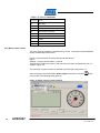
6.2.2 Motor Control Center
The User Guide is available in Install directory at URL :C:\Program Files\Atmel\Motor
Control Center\help\Overview.htm
First, the communication must be achieved with the MC303 :
Select :
Settings -> Target communication -> RS232
Then force the COM port number to the one which has been enumerated as cdc (i.e.
COM9 in Figure 10)
The AVR1607 Target must then be selected to get the right configuration : to
select,this target, execute the File > Select Target command or click the
in the toolbar. The following dialog pops up:
button
Figure 10. Motor Control Center Interface
16
AVR1607
8311A-AVR-07/10
AVR1607
7 USB communication
Communication can be achieved from PC to USB connector of MC303 board.
The AVR1014, MC303 Hardware User Guide details the configuration to be achieved.
Communication port becomes a Virtual Com port which must be forced in RS232
Settings window.
Same tools and commands as described in section 6 can be used through this Virtual
Com port.
17
8311A-AVR-07/10
Disclaimer
Headquarters
International
Atmel Corporation
2325 Orchard Parkway
San Jose, CA 95131
USA
Tel: 1(408) 441-0311
Fax: 1(408) 487-2600
Atmel Asia
Unit 1-5 & 16, 19/F
BEA Tower, Millennium City 5
418 Kwun Tong Road
Kwun Tong, Kowloon
Hong Kong
Tel: (852) 2245-6100
Fax: (852) 2722-1369
Atmel Europe
Le Krebs
8, Rue Jean-Pierre Timbaud
BP 309
78054 Saint-Quentin-enYvelines Cedex
France
Tel: (33) 1-30-60-70-00
Fax: (33) 1-30-60-71-11
Atmel Japan
9F, Tonetsu Shinkawa Bldg.
1-24-8 Shinkawa
Chuo-ku, Tokyo 104-0033
Japan
Tel: (81) 3-3523-3551
Fax: (81) 3-3523-7581
Technical Support
[email protected]
Sales Contact
www.atmel.com/contacts
Product Contact
Web Site
http://www.atmel.com/
Literature Request
www.atmel.com/literature
Disclaimer: The information in this document is provided in connection with Atmel products. No license, express or implied, by estoppel or otherwise, to any
intellectual property right is granted by this document or in connection with the sale of Atmel products. EXCEPT AS SET FORTH IN ATMEL’S TERMS AND
CONDITIONS OF SALE LOCATED ON ATMEL’S WEB SITE, ATMEL ASSUMES NO LIABILITY WHATSOEVER AND DISCLAIMS ANY EXPRESS, IMPLIED
OR STATUTORY WARRANTY RELATING TO ITS PRODUCTS INCLUDING, BUT NOT LIMITED TO, THE IMPLIED WARRANTY OF MERCHANTABILITY,
FITNESS FOR A PARTICULAR PURPOSE, OR NON-INFRINGEMENT. IN NO EVENT SHALL ATMEL BE LIABLE FOR ANY DIRECT, INDIRECT,
CONSEQUENTIAL, PUNITIVE, SPECIAL OR INCIDENTAL DAMAGES (INCLUDING, WITHOUT LIMITATION, DAMAGES FOR LOSS OF PROFITS,
BUSINESS INTERRUPTION, OR LOSS OF INFORMATION) ARISING OUT OF THE USE OR INABILITY TO USE THIS DOCUMENT, EVEN IF ATMEL HAS
BEEN ADVISED OF THE POSSIBILITY OF SUCH DAMAGES. Atmel makes no representations or warranties with respect to the accuracy or completeness of the
contents of this document and reserves the right to make changes to specifications and product descriptions at any time without notice. Atmel does not make any
commitment to update the information contained herein. Unless specifically provided otherwise, Atmel products are not suitable for, and shall not be used in,
automotive applications. Atmel’s products are not intended, authorized, or warranted for use as components in applications intended to support or sustain life.
®
®
®
© 2010 Atmel Corporation. All rights reserved. Atmel , Atmel logo and combinations thereof, AVR , AVR logo and others, are the
registered trademarks, XMEGATM and others are trademarks of Atmel Corporation or its subsidiaries. Other terms and product names may be
trademarks of others.
8311A-AVR-07/10
Mouser Electronics
Authorized Distributor
Click to View Pricing, Inventory, Delivery & Lifecycle Information:
Atmel:
ATAVRMC323