1
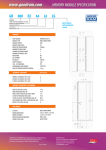
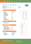
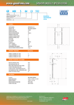
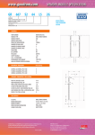
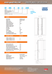
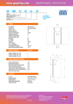
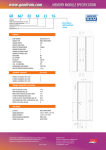
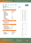
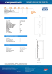
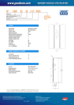
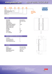
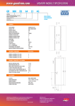
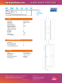
www.goodram.com
GR
800
D2
64
MEMORY MODULE SPECIFICATION
L6
4G
GOODRAM
SPEED / DATA TRANSFER 800MHz / PC2-6400
MODULE TYPE DDR2 SDRAM DIMM
MODULE DATA WIDTH 64
CAS LATENCY 6
MODULE DENSITY 4GB
professional memory for everyone
DDR II MODULE
PART NUMBERING
SYSTEM
PIN 64
PIN 65
PIN 120
6
6
6
18
PIN 1
CAS LATENCY
RAS# TO CAS# DELAY, tRCD
ROW PRECHARGE TIME, tRP
ACTIVE TO PRECHARGE TIME, tRAS
PIN 240
DYNAMIC PARAMETERS FOR 800MHz
PIN 185
GR800D264L6/4G
DDR2 SDRAM DIMM
4GB
64
256Mx8
16
2
2
NO
NO
240 PIN
1,8V
YES
PIN 184
PART NUMBER
MODULE TYPE
MODULE DENSITY
MODULE DATA WIDTH
DRAM CHIP ORAGNIZATION
NUMBER OF DRAM CHIPS
NUMBER OF MODULE RANKS
NUMBER OF MODULE SIDES
REGISTERED
ECC SUPPORT
PIN COUNT
SUPPLY VOLTAGE
SSTL_18 COMPATIBLE
PIN 121
FEATURES
4.00
f2,50 (2x)
PCB DETAILS
17,78
30,00
GOODRAM logo and GOODDRIVE logo are registered trademarks of Wilk Elektronik S.A.
All other trademarks and logos are the property of their respective owners.
All products and specifications are subject to change without notice.
Rev. 20.05.2010
Wilk Elektronik S.A.
Poland, 43-174 £aziska Górne, ul. Miko³owska 42
tel.: 0-32/ 736 90 00, fax: 0-32/ 736 90 01
www.wilk.com.pl l www.goodram.com
© Wilk Elektronik S.A. 2007
133,35
63,00
2,31
10,00
128,70
2,92
131,34
DDR2 SDRAM DIMM
133,35 x 30mm ± 0,1mm
1,27mm ± 0,13mm
FBGA, x8bit
GOLD PLATED
6
,7
R0
PCB TYPE
BOARD DIMENSIONS
BOARD THICKNESS
DRAM PACKAGE INFORMATION
CONTACT PADS (PIN)
www.goodram.com
MEMORY MODULE SPECIFICATION
SPD CONFIGURATION
BYTE
DESCRIPTION
HEX
DEC
0
1
2
3
4
5
6
7
8
9
10
11
12
13
14
15
16
17
18
19
20
21
22
23
24
25
26
27
28
29
30
31
32
33
34
35
36
37
38
39
40
41
42
43
44
45
46
47
48
49
50
51
52
53
54
55
56
57
58
59
60
61
62
63
Number of Serial PD Bytes written during module production
Total number of Bytes in Serial PD device
Fundamental Memory Type (FPM, EDO, SDRAM …)
Number of Row Addresses on this assembly
Number of Column Addresses on this assembly
Number of DIMM Banks
Data Width of this assembly
Data Width of this assembly
Voltage Interface Level of this assembly
SDRAM Cycle time at Maximum Supported CAS Latency (CL), CL=X
SDRAM Access from Clock
DIMM configuration type (Non-parity, Parity or ECC)
Refresh Rate/Type
Primary SDRAM Width
Error Checking SDRAM Width
SDRAM Device Attributes: Minimum Clock Delay, Back-to-Back RCA
SDRAM Device Attributes: Burst Lengths Supported
SDRAM Device Attributes: Number of Banks on SDRAM Device
SDRAM Device Attributes: CAS Latency
SDRAM Device Attributes: CS Latency
SDRAM Device Attributes: Write Latency/DIMM Type Information
SDRAM Module Attributes
SDRAM Device Attributes: General
Minimum Clock Cycle at CL = X - 0.5
Maximum Data Access Time (tAC) from Clock at CL = X - 0.5
Minimum Clock Cycle at CL = X - 1
Maximum Data Access Time (tAC) from Clock at CL = X - 1
Minimum Row Precharge Time (tRP)
Minimum Row Active to Row Active delay (tRRD)
Minimum RAS to CAS delay (tRCD)
Minimum Active to Precharge Time (tRAS)
Module Bank Density
Address and Command Input Setup Time Before Clock
Address and Command Input Hold Time After Clock
Data Input Setup Time Before Clock
Data Input Hold Time After Clock
Write recovery time (tWR)
Internal write to read command delay (tWTR)
Internal read to precharge command delay (tRTP)
Memory Analysis Probe Characteristics
Extension of Byte 41 tRC and Byte 42 tRFC
SDRAM Device Minimum Active to Active/Auto Refresh Time (tRC)
SDRAM Device Minimum Auto Refresh to Active/Auto Refresh (tRFC)
SDRAM Device Maximum device cycle time (tCKmax)
SDRAM Device Maximum skew between DQS and DQ signals (tDQSQ)
DDR SDRAM Device Maximum Read Data Hold Skew Factor (tQHS)
Reserved for future use
SDRAM Device Attributes - DDR SDRAM DIMM Height
Reserved for future use
Reserved for future use
Reserved for future use
Reserved for future use
Reserved for future use
Reserved for future use
Reserved for future use
Reserved for future use
Reserved for future use
Reserved for future use
Reserved for future use
Reserved for future use
Reserved for future use
Reserved for future use
SPD Revision
Checksum for Bytes 0-62
0x80
0x08
0x08
0x0F
0x0A
0x61
0x40
0x00
0x05
0x25
0x40
0x00
0x82
0x08
0x00
0x00
0x0C
0x08
0x70
0x01
0x02
0x00
0x07
0x30
0x45
0x3D
0x50
0x3C
0x1E
0x3C
0x2D
0x02
0x17
0x25
0x05
0x12
0x3C
0x1E
0x1E
0x00
0x30
0x39
0xC3
0x80
0x14
0x1E
0x0F
0x50
0x60
0x5F
0x44
0x43
0x31
0x49
0x2F
0x72
0x3A
0x43
0x00
0x00
0x00
0x00
0x12
0x8B
128
8
8
15
10
97
64
0
5
37
64
0
130
8
0
0
12
8
112
1
2
0
7
48
69
61
80
60
30
60
45
2
23
37
5
18
60
30
30
0
48
57
195
128
20
30
15
80
96
95
68
67
49
73
47
114
58
67
0
0
0
0
18
139
64-255
Manufacturer’s specific data
GOODRAM logo and GOODDRIVE logo are registered trademarks of Wilk Elektronik S.A.
All other trademarks and logos are the property of their respective owners.
All products and specifications are subject to change without notice.
Rev. 20.05.2010
Wilk Elektronik S.A.
Poland, 43-174 £aziska Górne, ul. Miko³owska 42
tel.: 0-32/ 736 90 00, fax: 0-32/ 736 90 01
www.wilk.com.pl l www.goodram.com
© Wilk Elektronik S.A. 2007
professional memory for everyone