1
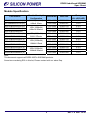
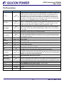
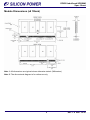
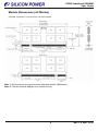
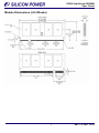
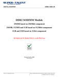
DDR2 Unbuffered SODIMM
Spec Sheet
Features
•200-pin, Small-Outline Dual In-line Memory Module (SODIMM)
• Fast data transfer rates: PC2-4200, PC2-5300, or PC2-6400
• 512MB (64Mx64), 1GB (128 Meg x 64), 2GB (256 Meg x 64)
• JEDEC standard 1.8V I/O (SSTL_18-compatible)
• VDD = 1.8 V ±0.1V (SSTL_18)
• VDDSPD = +1.7V to +3.6V
• Differential clock inputs, Differential data strobe (DQS, DQS#) option
• 4n-bit prefetch architecture
• Multiple internal device banks for concurrent operation
• Programmable CAS latency (CL)
• Posted CAS additive latency (AL)
• WRITE latency = READ latency - 1 tCK
• Programmable burst lengths (BL): 4 or 8
• Adjustable data-output drive strength
• 64ms, 8,192-cycle refresh
• On-die termination (ODT)
• Serial presence-detect (SPD) with EEPROM
• Gold edge contacts
1
Rev 1.0 Nov. 2010
DDR2 Unbuffered SODIMM
Spec Sheet
Module Specification
Part Number
SP512MBSRU533O01(2)
SP512MBSRU667O01(2)
SP001GBSRU533Q01(2)
SP001GBSRU667Q01(2)
SP001GBSRU800Q02
SP001GBSRU667O01(2)
SP001GBSRU800O01
SP001GBSRU533S01(2)
SP001GBSRU667S01(2)
SP001GBSRU800S01(2)
SP002GBSRU533S01(2)
SP002GBSRU667S01(2)
SP002GBSRU800S01(2)
Module Density &
Configuration
512MB (64Mx64)
64Mx8 1Rank
1GB (128Mx64)
64Mx16 2Ranks
1GB (128Mx64)
64Mx8 2Ranks
1GB (256Mx64)
128Mx8 1Rank
2GB (256Mx64)
128Mx8 2Ranks
Bandwidth
Data Rate
Timing
(tCL-tRCD-tRP)
PC2-4200
DDR2-533
4-4-4
PC2-5300
DDR2-667
5-5-5
PC2-4200
DDR2-533
4-4-4
PC2-5300
DDR2-667
5-5-5
PC2-6400
DDR2-800
5-5-5
PC2-5300
DDR2-667
5-5-5
PC2-6400
DDR2-800
5-5-5
PC2-4200
DDR2-533
4-4-4
PC2-5300
DDR2-667
5-5-5
PC2-6400
DDR2-800
5-5-5
PC2-4200
DDR2-533
4-4-4
PC2-5300
DDR2-667
5-5-5
PC2-6400
DDR2-800
5-5-5
Note:
This document supports all DDR2 200Pin SODIMM products.
Some item was being EOL in this list, Please contact with our sales Dep.
2
Rev 1.0 Nov. 2010
DDR2 Unbuffered SODIMM
Spec Sheet
Pin Assignments
200-Pin DDR2 SODIMM Front
200-Pin DDR2 SODIMM Back
Pin
Symbol
Pin
Symbol
Pin
Symbol
Pin
Symbol
Pin
Symbol
Pin
Symbol
Pin
Symbol
Pin
Symbol
1
51
DQ1
57
9
VSS
59
11
DQS0#
61
13
DQS0
63
15
VSS
65
17
DQ2
67
117
19
DQ3
VSS
DQ8
DQ9
VSS
DQS1#
DQS1
VSS
DQ10
DQ11
VSS
VSS
DQ16
DQ17
VSS
DQS2#
69
83
85
BA2
135
87
VDD
A12
A9
A8
VDD
A5
A3
137
A0
VDD
BA1
RAS#
S0#
VDD
ODT0
A13
VDD
NC
VSS
DQ36
DQ37
VSS
DM4
VSS
DQ38
DQ39
VSS
DQ44
DQ45
VSS
DQS5#
DQS5
VSS
152
7
DM2
VSS
DQ22
DQ23
VSS
DQ28
DQ29
VSS
DQS3#
DQS3
VSS
DQ30
DQ31
VSS
CKE1
VDD
NC
NC
VDD
A11
A7
A6
VDD
A4
A2
102
55
VSS
DQ4
DQ5
VSS
DM0
VSS
DQ6
DQ7
VSS
DQ12
DQ13
VSS
DM1
VSS
CK0
CK0#
VSS
DQ14
DQ15
VSS
VSS
DQ20
DQ21
VSS
NC
52
DQ0
DQ42
DQ43
VSS
DQ48
DQ49
VSS
NC
VSS
DQS6#
DQS6
VSS
DQ50
DQ51
VSS
DQ56
DQ57
VSS
DM7
VSS
DQ58
DQ59
VSS
SDA
SCL
VDDSPD
2
5
A1
VDD
A10
BA0
WE#
VDD
CAS#
S1#
VDD
ODT1
VSS
DQ32
DQ33
VSS
DQS4#
DQS4
VSS
DQ34
DQ35
VSS
DQ40
DQ41
VSS
DM5
VSS
151
53
DQS2
VSS
DQ18
DQ19
VSS
DQ24
DQ25
VSS
DM3
NC
VSS
DQ26
DQ27
VSS
CKE0
VDD
NC
101
3
VREF
VSS
DQ46
DQ47
VSS
DQ52
DQ53
VSS
CK1
CK1#
VSS
DM6
VSS
DQ54
DQ55
VSS
DQ60
DQ61
VSS
DQS7#
DQS7
VSS
DQ62
DQ63
VSS
SA0
SA1
21
23
25
27
29
31
33
35
37
39
41
43
45
47
49
71
73
75
77
79
81
89
91
93
95
97
99
103
105
107
109
111
113
115
119
121
123
125
127
129
131
133
139
141
143
145
147
149
153
155
157
159
161
163
165
167
169
171
173
175
177
179
181
183
185
187
189
191
193
195
197
199
4
6
8
10
12
14
16
18
20
22
24
26
28
30
32
34
36
38
40
42
44
46
48
50
3
54
56
58
60
62
64
66
68
70
72
74
76
78
80
82
84
86
88
90
92
94
96
98
100
104
106
108
110
112
114
116
118
120
122
124
126
128
130
132
134
136
138
140
142
144
146
148
150
154
156
158
160
162
164
166
168
170
172
174
176
178
180
182
184
186
188
190
192
194
196
198
200
Rev 1.0 Nov. 2010
DDR2 Unbuffered SODIMM
Spec Sheet
Pin Description
Symbol
Type
A0–A13
Input
(SSTL_18)
BA0–BA2
Input
(SSTL_18)
CK0, CK0#,
CK1, CK1#,
CK2, CK2#
Input
(SSTL_18)
CKE0 ,CKE1
Input
(SSTL_18)
ODT0, ODT1
Input
(SSTL_18)
RAS#, CAS#,
WE#
Input
(SSTL_18)
Input
(SSTL_18)
Input
(SSTL_18)
Input
(SSTL_18)
S0#, S1#
SA0–SA2
SCL
SDA
I/O
DM0–DM7
I/O
(SSTL_18)
DQ0–DQ63
I/O
(SSTL_18)
DQS0–DQS7,
DQS0#–DQS7#
I/O
(SSTL_18)
Description
Address inputs: Provide the row address for ACTIVE commands, and the column
address and auto precharge bit (A10) for READ/WRITE commands, to select one
location out of the memory array in the respective bank. A10 sampled during a
PRECHARGE command determines whether the PRECHARGE applies to one
device bank (A10 LOW, device bank selected by BA0–BA2) or all device banks
(A10 HIGH). The address inputs also provide the op-code during a LOAD MODE
command. A0–A12 (256MB) and A0–A13 (512MB, 1GB).
Bank address inputs: BA0–BA2 define to which device bank an ACTIVE, READ,
WRITE, or PRECHARGE command is being applied. BA0–BA2 define which mode
register, including MR, EMR, EMR(2), and EMR(3), is loaded during the LOAD
MODE command. BA0, BA1 (256MB, 512MB) and BA0–BA2 (1GB).
Clock: CK and CK# are differential clock inputs. All address and control input
signals are sampled on the crossing of the positive edge of CK and the negative
edge of CK#. Output data (DQs and DQS/DQS#) is referenced to the crossings of
CK and CK#.
Clock enable: CKE (registered HIGH) activates and CKE (registered LOW)
deactivates clocking circuitry on the DDR2 SDRAM.
On-die termination: ODT (registered HIGH) enables termination resistance
internal to the DDR2 SDRAM. When enabled, ODT is only applied to the following
pins: DQ, DQS, DQS#, and CB. The ODT input will be ignored if disabled via the
LOAD MODE command.
Command inputs: RAS#, CAS#, and WE# (along with S#) define the command
being entered.
Chip select: S# enables (registered LOW) and disables (registered HIGH) the
command decoder.
Presence-detect address inputs: These pins are used to configure the
presence-detect devices.
Serial clock for presence-detect: SCL is used to synchronize the presence-detect
data transfer to and from the module.
Serial presence-detect data: SDA is a bidirectional pin used to transfer addresses
and data into and out of the presence-detect portion of the module.
Data input mask: DM is an input mask signal for write data. Input data is masked
when DM is sampled HIGH, along with that input data, during a write access. DM is
sampled on both edges of DQS. Although DM pins are input-only, the DM loading is
designed to match that of DQ and DQS pins.
Data input/output: Bidirectional data bus.
VDD/VDDQ
Supply
Data strobe: Output with read data, input with write data for source synchronous
operation. Edge-aligned with read data, center-aligned with write data. DQS# is only
used when differential data strobe mode is enabled via the LOAD MODE command.
Power supply: 1.8V ±0.1V.
VDDSPD
Supply
Serial EEPROM positive power supply: +1.7V to +3.6V.
VREF
Supply
SSTL_18 reference voltage. (VDD/2)
VSS
Supply
Ground.
NC
–
No connect: These pins are not connected on the module.
4
Rev 1.0 Nov. 2010
DDR2 Unbuffered SODIMM
Spec Sheet
Module Dimensions (x8 1Rank)
Note 1: All dimensions are typical unless otherwise stated. (Millimeters)
Note 2: The dimensional diagram is for reference only
5
Rev 1.0 Nov. 2010
DDR2 Unbuffered SODIMM
Spec Sheet
Module Dimensions (x8 2Ranks)
X64 DIMM, populated as one physical rank of x8 DDR2 SDRAMs
Note 1: All dimensions are typical unless otherwise stated. (Millimeters)
Note 2: The dimensional diagram is for reference only
6
Rev 1.0 Nov. 2010
DDR2 Unbuffered SODIMM
Spec Sheet
Module Dimensions (x16 2Ranks)
7
Rev 1.0 Nov. 2010