1
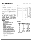
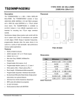
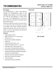
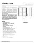
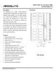
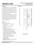
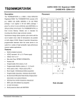
172PIN DDR2 533 Micro-DIMM
1024MB With 64Mx16 CL4
TS1GPA1024U5
Description
Placement
The TS1GPA1024U5 is a 128M x 64bits DDR2-533
Micro-DIMM. The TS1GPA1024U5 consists of 8pcs
64Mx16bits DDR2 SDRAMs in 92 ball FBGA packages
and a 2048 bits serial EEPROM on a 172-pin printed
circuit board. The TS1GPA1024U5 is available as
non-ECC module in 2-row 128Mx64 organization and is
intended for mounting into 172-pin edge connector
sockets.
C B A
Synchronous design allows precise cycle control with the
use of system clock. Data I/O transactions are possible
D
on both edges of DQS. Range of operation frequencies,
E
programmable latencies allow the same device to be
F
G
useful for a variety of high bandwidth, high performance
memory system applications.
PCB: 09-2420
Features
•
RoHS compliant products.
•
JEDEC standard 1.8V ± 0.1V Power supply
•
VDDQ=1.8V ± 0.1V
•
Max clock Freq: 267MHZ; 533Mb/s/Pin.
•
Posted CAS
•
Programmable CAS Latency: 3,4,5
•
Programmable Additive Latency :0, 1,2,3 and 4
•
Write Latency (WL) = Read Latency (RL)-1
•
Burst Length: 4,8(Interleave/nibble sequential)
•
Programmable sequential / Interleave Burst Mode
•
Bi-directional Differential Data-Strobe (Single-ended
data-strobe is an optional feature)
•
Off-Chip Driver (OCD) Impedance Adjustment
•
MRS cycle with address key programs.
•
On Die Termination
•
Serial presence detect with EEPROM
Transcend Information Inc.
1
H
172PIN DDR2 533 Micro-DIMM
1024MB With 64Mx16 CL4
TS1GPA1024U5
Dimensions
Side
A
Pin Identification
Millimeters
Inches
Symbol
45.50 ± 0.20 1.791 ± 0.008
Function
A0~A12, BA0~BA2
Address input
B
44.50
1.752
DQ0~DQ63
Data Input / Output.
C
42.50
1.673
DQS0~DQS7
Data strobe
D
1.00
0.039
/DQS0~/DQS7
Differential Data strobe
E
2.75± 0.10
0.108± 0.004
F
15.00
0.591
CK0, /CK0
Clock Input.
G
30.00± 0.20
0.984± 0.008
CKE0, CKE1
Clock Enable Input.
H
0.80 ± 0.10
0.031 ± 0.004
ODT0, ODT1
On-die termination control line
/CS0, /CS1
Chip Select Input.
/RAS
Row Address Strobe
/CAS
Column Address Strobe
/WE
Write Enable
DM0~DM7
Data-in Mask
VDD
+1.8 Voltage power supply
(Refer Placement)
+1.8 Voltage Power Supply for
VDDQ
DQS
VREF
Power Supply for Reference
Serial EEPROM Positive Power
VDDSPD
Supply
Transcend Information Inc.
2
SCL
Serial PD Clock
SDA
Serial PD Add/Data input/output
VSS
Ground
NC
No Connection