1
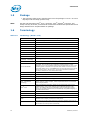
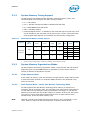
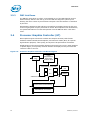
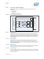
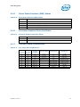
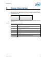
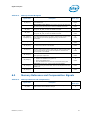
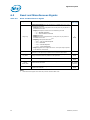
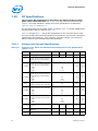
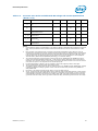
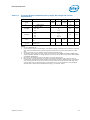
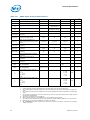
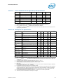
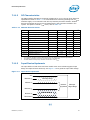
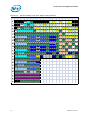
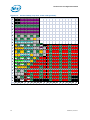
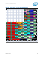
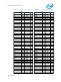
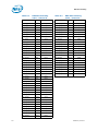
Signal Description
6.1
System Memory Interface Signals
Table 6-2.
Memory Channel A Signals
Signal Name
Bank Select: These signals define which banks are selected within
each SDRAM rank.
O
DDR3
SA_WE#
Write Enable Control Signal: This signal is used with SA_RAS# and
SA_CAS# (along with SA_CS#) to define the SDRAM Commands.
O
DDR3
SA_RAS#
RAS Control Signal: This signal is used with SA_CAS# and SA_WE#
(along with SA_CS#) to define the SRAM Commands.
O
DDR3
SA_CAS#
CAS Control Signal: This signal is used with SA_RAS# and SA_WE#
(along with SA_CS#) to define the SRAM Commands.
O
DDR3
SA_DQS[8:0]
SA_DQS#[8:0]
Data Strobes: SA_DQS[8:0] and its complement signal group make
up a differential strobe pair. The data is captured at the crossing point
of SA_DQS[8:0] and its SA_DQS#[8:0] during read and write
transactions.
I/O
DDR3
SA_BS[2:0]
Data Bus: Channel A data signal interface to the SDRAM data bus.
I/O
DDR3
SA_MA[15:0]
Memory Address: These signals are used to provide the multiplexed
row and column address to the SDRAM.
O
DDR3
SA_CK[3:0]
SDRAM Differential Clock: Channel A SDRAM Differential clock signal
pair. The crossing of the positive edge of SA_CK and the negative edge
of its complement SA_CK# are used to sample the command and
control signals on the SDRAM.
O
DDR3
SA_CK#[3:0]
SDRAM Inverted Differential Clock: Channel A SDRAM Differential
clock signal-pair complement.
O
DDR3
SA_CKE[3:0]
Clock Enable: (1 per rank). Used to:
• Initialize the SDRAMs during power-up
• Power-down SDRAM ranks
• Place all SDRAM ranks into and out of self-refresh during STR
O
DDR3
SA_CS#[3:0]
Chip Select: (1 per rank). Used to select particular SDRAM
components during the active state. There is one Chip Select for each
SDRAM rank.
O
DDR3
SA_DQ[63:0]
SA_ODT[3:0]
62
Direction/
Buffer Type
Description
On Die Termination: Active Termination Control.
O
DDR3
Datasheet, Volume 1