1
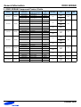
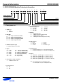
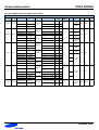
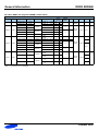
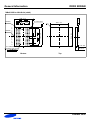
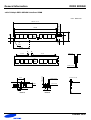
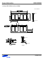
General Information
DDR3 SDRAM
DDR3 SDRAM Product Guide
October 2009
Memory Division
October 2009
General Information
DDR3 SDRAM
1. DDR3 SDRAM Component Ordering Information
1
2
3
4
5
6
7
8
9
10
11
K 4 B X X X X X X X - X X X X
Speed
SAMSUNG Memory
DRAM
Temp & Power
DRAM Type
Package Type
Density
Revision
Interface (VDD, VDDQ)
Bit Organization
# of Internal Banks
1. SAMSUNG Memory : K
7. Interface ( VDD, VDDQ)
6 : SSTL (1.5V, 1.5V)
2. DRAM : 4
8. Revision
3. DRAM Type
B : DDR3 SDRAM
4. Density
51 : 512Mb
1G :
1Gb
2G :
2Gb
4G :
4Gb
M
A
B
C
D
E
F
G
H
: 1st Gen.
: 2nd Gen.
: 3rd Gen.
: 4th Gen.
: 5th Gen.
: 6th Gen.
: 7th Gen
: 8th Gen
: 9th Gen
9. Package Type
5. Bit Organization
04 : x 4
08 : x 8
16 : x16
Z
H
J
M
:
:
:
:
FBGA (Lead-free)
FBGA (Halogen-free & Lead-free)
FBGA (Lead-free, DDP)
FBGA (Halogen-free & Lead-free, DDP)
10. Temp & Power
C : Commercial Temp.( 0°C ~ 85°C) & Normal Power
L : Commercial Temp.( 0°C ~ 85°C) & Low Power
Y : Commercial Temp.( 0°C ~ 85°C) & Low VDD(1.35V)
6. # of Internal Banks
3 : 4 Banks
4 : 8 Banks
5 : 16 Banks
11. Speed
F7 : DDR3-800
F8 : DDR3-1066
H9 : DDR3-1333
K0 : DDR3-1600
(400MHz @ CL=6, tRCD=6, tRP=6)
(533MHz @ CL=7, tRCD=7, tRP=7)
(667MHz @ CL=9, tRCD=9, tRP=9)
(800MHz @ CL=11, tRCD=11, tRP=11)
October 2009
General Information
DDR3 SDRAM
2. DDR3 SDRAM Component Product Guide
Density
1Gb D-die
1Gb E-die
1Gb F-die
2Gb B-die
2Gb C-die
Banks
8Banks
8Banks
8Banks
8Banks
8Banks
DDP 2Gb D-die
8Banks
DDP 2Gb E-die
8Banks
DDP 4Gb B-die
8Banks
Part Number
Package & Power,
Temp. (-C/-L) & Speed
Org.
K4B1G0446D
HC(L)F7/F8/H9
256M x 4
K4B1G0846D
HC(L)F7/F8/H9
128M x 8
K4B1G1646D
HC(L)F7/F8/H9
64M x 16
K4B1G0446E
HC(L)F7/F8/H9/K0
256M x 4
K4B1G0846E
HC(L)F7/F8/H9/K0
128M x 8
K4B1G1646E
HC(L)F7/F8/H9/K0
64M x 16
K4B1G0446E
HYF7/F8/H9/K0
256M x 4
K4B1G0846E
HYF7/F8/H9/K0
128M x 8
K4B1G0446F
HC(L)F8/H9
256M x 4
K4B1G0846F
HC(L)F8/H9
128M x 8
K4B1G0446F
HY(L)F8/H9
256M x 4
K4B1G0846F
HY(L)F8/H9
128M x 8
K4B2G0446B
HC(L)F7/F8/H9
512M x 4
K4B2G0846B
HC(L)F7/F8/H9
256M x 8
K4B2G1646B
HC(L)F7/F8/H9
128M x 16
K4B2G0446B
HYF7/F8/H9
512M x 4
K4B2G0846B
HYF7/F8/H9
256M x 8
K4B2G0446C
HC(L)F8/H9
512M x 4
K4B2G0846C
HC(L)F8/H9
256M x 8
K4B2G0446C
HY(L)F8/H9
512M x 4
K4B2G0846C
HY(L)F8/H9
256M x 8
K4B2G0446D
MC(L)F7/F8/H9
512M x 4
K4B2G0846D
MC(L)F7/F8/H9
256M x 8
K4B2G0446E
MC(L)F7/F8/H9
512M x 4
K4B2G0846E
MC(L)F7/F8/H9
256M x 8
K4B4G0446B
MC(L)F7/F8/H9
1G x 4
K4B2G0846B
MC(L)F7/F8/H9
512M x 8
VDD Voltage
1.5V
PKG
78 + 4 ball
FBGA
Avail.
Note
Now
96 + 4 ball
FBGA
1.5V
78 ball
FBGA
96 ball
FBGA
1.35V
Now
78 ball
FBGA
1.5V
78 ball
FBGA
Now
1.35V
1.5V
78 ball
FBGA
96 ball
FBGA
1.35V
Now
78 ball
FBGA
1.5V
78 ball
FBGA
Now
1.5V
78 ball
FBGA
Now
1.5V
78 ball
FBGA
Now
1.5V
78 ball
FBGA
Now
1.35V
* Note : 1.35V product is 1.5V operatable.
October 2009
General Information
DDR3 SDRAM
3. DDR3 SDRAM Module Ordering Information
1
2
3
4
5
6
7
8
9
10
11
12
M X X X B X X X X X X X - X X X
Memory Module
DIMM Type
Data bits
Speed
DRAM Component Type
Temp & Power
Depth
PCB Revision
Package
# of Banks in Comp. & Interface
Component Revision
Bit Organization
1. Memory Module : M
8. Component Revision
M : 1st Gen.
B : 3rd Gen.
D : 5th Gen.
F : 7th Gen.
2. DIMM Type
3 : DIMM
4 : SODIMM
3. Data Bits
71 :
78 :
91 :
92 :
93 :
x64
x64
x72
x72
x72
204pin Unbuffered SODIMM
240pin Unbuffered DIMM
240pin ECC unbuffered DIMM
240pin VLP Registered DIMM
240pin Registered DIMM
A
C
E
G
:
:
:
:
2nd Gen.
4th Gen.
6th Gen.
8th Gen.
9. Package
: FBGA(Lead-free)
Z
: FBGA(Lead-free & Halogen-free)
H
: FBGA(Lead-free, DDP)
J
M : FBGA(Lead-free & Halogen-free, DDP)
10. PCB Revision
4. DRAM Component Type
0 : None
2 : 2nd Rev.
4 : 4th Rev.
1 : 1st Rev.
3 : 3rd Rev.
S : Reduced Layer
B : DDR3 SDRAM (1.5V VDD)
5. Depth
32 : 32M
64 : 64M
28 : 128M
56 : 256M
51 : 512M
1G : 1G
2G : 2G
33
65
29
57
52
1K
2K
: 32M (for 128Mb/512Mb)
: 64M (for 128Mb/512Mb)
: 128M (for 128Mb/512Mb)
: 256M (for 512Mb/2Gb)
: 512M (for 512Mb/2Gb)
: 1G (for 2Gb)
: 2G (for 2Gb)
6. # of Banks in comp. & Interface
7 :
11. Temp & Power
C : Commercial Temp.( 0°C ~ 85°C) & Normal Power
Y : Commercial Temp.( 0°C ~ 85°C) & Low VDD(1.35V)
12. Speed
F7 : DDR3-800
F8 : DDR3-1066
H9 : DDR3-1333
K0 : DDR3-1600
(400MHz @ CL=6, tRCD=6, tRP=6)
(533MHz @ CL=7, tRCD=7, tRP=7)
(667MHz @ CL=9, tRCD=9, tRP=9)
(800MHz @ CL=11, tRCD=11, tRP=11)
8Banks & SSTL-1.5V
Note: PC3-6400(DDR3-800),PC3-8500(DDR3-1066),
PC3-10600(DDR3-1333), PC3-12800(DDR3-1600)
7. Bit Organization
0 : x4
3 : x8
4 : x16
October 2009
General Information
DDR3 SDRAM
4. DDR3 SDRAM Module Product Guide
4.1 240Pin DDR3 Unbuffered DIMM (1.5V Product)
240Pin DDR3 Unbuffered DIMM
Org.
128Mx 64
128Mx 72
256Mx 64
256Mx 72
Density
1GB
1GB
2GB
2GB
512Mx 64
4GB
512Mx 72
4GB
Part Number
Speed
M378B2873DZ1
CF8/H9
M378B2873EH1
CF8/H9/K0
M378B2873FHS
Raw Card
Composition
Comp.
Version
128M x 8 * 8 pcs
1Gb
D-die
128M x 8 * 8 pcs
1Gb
E-die
CF8/H9
128M x 8 * 8 pcs
1Gb
F-die
M391B2873DZ1
CF8/H9
128M x 8 * 9 pcs
1Gb
D-die
M391B2873EH1
CF8/H9/K0
128M x 8 * 9 pcs
1Gb
E-die
M391B2873FH0
CF8/H9/K0
128M x 8 * 9 pcs
1Gb
F-die
M378B5673DZ1
CF8/H9
128M x 8 * 16 pcs
1Gb
D-die
M378B5673EH1
CF8/H9/K0
128M x 8 * 16 pcs
1Gb
E-die
M378B5673FH0
CF8/H9/K0
128M x 8 * 16 pcs
1Gb
F-die
M378B5773CHS
CF8/H9/K0
256M x 8 * 8 pcs
2Gb
C-die
M391B5673DZ1
CF8/H9
128M x 8 * 18 pcs
1Gb
D-die
M391B5673EH1
CF8/H9/K0
128M x 8 * 18 pcs
1Gb
E-die
M391B5673FH0
CF8/H9/K0
128M x 8 * 18 pcs
1Gb
F-die
M391B5773CH0
CF8/H9/K0
M378B5273BH1
CF8/H9
M378B5273CH0
CF8/H9/K0
M391B5273BH1
CF8/H9
M391B5273CH0
CF8/H9/K0
A(1Rx8)
D(1Rx8)
B(2Rx8)
A(1Rx8)
E(2Rx8)
D(1Rx8)
B(2Rx8)
E(2Rx8)
256M x 8 * 9 pcs
2Gb
C-die
256M x 8 * 16 pcs
2Gb
B-die
256M x 8 * 16 pcs
2Gb
C-die
256M x 8 * 18 pcs
2Gb
B-die
256M x 8 * 18 pcs
2Gb
C-die
Internal
Banks
Rank
PKG
Height
Avail.
30mm
Now
30mm
Now
30mm
Now
30mm
Now
Note
78 + 4 ball
FBGA
8
1
78 ball
FBGA
78 + 4 ball
FBGA
8
1
78 ball
FBGA
78 + 4 ball
FBGA
8
2
78 ball
FBGA
8
1
78 + 4 ball
FBGA
8
2
78 ball
FBGA
1
8
2
78 ball
FBGA
30mm
Now
8
2
78 ball
FBGA
30mm
Now
Internal
Banks
Rank
PKG
Height
Avail.
8
1
78 ball
FBGA
30mm
Now
8
2
78 ball
FBGA
30mm
Now
8
1
8
2
78 ball
FBGA
30mm
Now
4.2 240Pin DDR3 Unbuffered DIMM (1.35V Product)
240Pin DDR3 Unbuffered DIMM
Org.
Density
128Mx 72
1GB
256Mx 72
512Mx 72
2GB
4GB
Part Number
Speed
M391B2873EH1
YF8/H9
M391B2873FH0
YF8/H9
M391B5673EH1
YF8/H9
M391B5673FH0
YF8/H9
M391B5773CH0
YF8/H9
M391B5273BH1
YF8/H9
M391B5273CH0
YF8/H9
Raw Card
D(1Rx8)
E(2Rx8)
D(1Rx8)
E(2Rx8)
Composition
Comp.
Version
128M x 8 * 9 pcs
1Gb
E-die
128M x 8 * 9 pcs
1Gb
F-die
128M x 8 * 18 pcs
1Gb
E-die
128M x 8 * 18 pcs
1Gb
F-die
256M x 8 * 9 pcs
2Gb
C-die
256M x 8 * 18 pcs
2Gb
B-die
256M x 8 * 18 pcs
2Gb
C-die
Note
* Note : 1.35V product is 1.5V operatable.
October 2009
General Information
DDR3 SDRAM
4.3 204Pin DDR3 SoDIMM (1.5V Product)
204Pin DDR3 SODIMM
Org.
128Mx 64
256Mx 64
512Mx 64
Density
1GB
2GB
4GB
Comp.
Version
Internal
Banks
Rank
PKG
D-die
8
2
96 + 4 ball
FBGA
1Gb
E-die
8
1
78 ball
FBGA
64M x 16 * 8 pcs
1Gb
E-die
8
2
96 ball
64M x 16 * 8 pcs
1Gb
F-die
8
1
78 ball
FBGA
128M x 8 * 16 pcs
1Gb
D-die
128M x 8 * 16 pcs
1Gb
E-die
128M x 8 * 16 pcs
1Gb
F-die
Part Number
Speed
Raw Card
M471B2874DZ1
CF8/H9
A(2Rx16)
64M x 16 * 8 pcs
1Gb
M471B2873EH1
CF8/H9
B(1Rx8)
128M x 8 * 8 pcs
M471B2874EH1
CF8/H9
A(2Rx16)
M471B2873FHS
CF8/H9
B(1Rx8)
M471B5673DZ1
CF8/H9
M471B5673EH1
CF8/H9
M471B5673FH0
CF8/H9
M471B5773CHS
CF8/H9
M471B5273BH1
CF8/H9
M471B5273CH0
CF8/H9
F(2Rx8)
B(1Rx8)
F(2Rx8)
Composition
256M x 8 * 8 pcs
2Gb
C-die
256M x 8 * 16 pcs
2Gb
B-die
256M x 8 * 16 pcs
2Gb
C-die
Height
Avail.
30mm
Now
30mm
Now
30mm
Now
Note
78 + 4 ball
FBGA
8
2
78 ball
FBGA
8
1
8
2
Internal
Banks
Rank
PKG
78 ball
FBGA
4.4 204Pin DDR3 SoDIMM (1.35V Product)
204Pin DDR3 SODIMM
Org.
128Mx 64
Density
1GB
Speed
Raw Card
Composition
M471B2873EH1
YF8/H9
B(1Rx8)
128M x 8 * 8 pcs
1Gb
E-die
8
1
78 ball
FBGA
M471B2874EH1
YF8/H9
A(1Rx16)
64M x 16 * 8 pcs
1Gb
E-die
8
2
96 ball
8
1
78 ball
FBGA
8
2
8
1
8
2
M471B2873FHS
256Mx 64
512Mx 64
2GB
4GB
Comp.
Version
Part Number
YF8/H9
M471B5673EH1
YF8/H9
M471B5673FH0
YF8/H9
M471B5773CHS
YF8/H9
M471B5273BH1
YF8/H9
M471B5273CH0
YF8/H9
B(1Rx8)
F(2Rx8)
B(1Rx8)
F(2Rx8)
128M x 8 * 8 pcs
1Gb
F-die
128M x 8 * 16 pcs
1Gb
E-die
128M x 8 * 16 pcs
1Gb
F-die
256M x 8 * 8 pcs
2Gb
C-die
256M x 8 * 16 pcs
2Gb
B-die
256M x 8 * 16 pcs
2Gb
C-die
Height
Avail.
30mm
Now
78 ball
FBGA
30mm
Now
78 ball
FBGA
30mm
Now
Note
* Note : 1.35V product is 1.5V operatable.
October 2009
General Information
DDR3 SDRAM
4.5 240Pin DDR3 Registered DIMM (1.5V Product)
240Pin DDR3 Registered DIMM
Org.
128Mx 72
256Mx 72
512Mx 72
Density
1GB
2GB
4GB
Part Number
Speed
M393B2873DZ1
CF8/H9
M393B2873EH1
CF8/H9
M393B2873FH0
Raw Card
2Gx 72
8GB
Comp.
Version
128M x 8 * 9 pcs
1Gb
D-die
128M x 8 * 9 pcs
1Gb
E-die
CF8/H9
128M x 8 * 9 pcs
1Gb
F-die
M393B5673DZ1
CF8/H9
128M x 8 * 18 pcs
1Gb
D-die
M393B5673EH1
CF8/H9
128M x 8 * 18 pcs
1Gb
E-die
M393B5673FH0
CF8/H9
128M x 8 * 18 pcs
1Gb
F-die
M393B5670DZ1
CF8/H9
256M x 4 * 18 pcs
1Gb
D-die
M393B5670EH1
CF8/H9
256M x 4 * 18 pcs
1Gb
E-die
M393B5670FH0
CF8/H9
256M x 4 * 18 pcs
1Gb
F-die
M393B5173DZ1
CF7/F8
128M x 8 * 36 pcs
1Gb
D-die
M393B5173EH1
CF7/F8
128M x 8 * 36 pcs
1Gb
E-die
M393B5173FH0
CF7/F8
128M x 8 * 36 pcs
1Gb
F-die
M393B5170DZ1
CF8/H9
256M x 4 * 36 pcs
1Gb
D-die
M393B5170EH1
CF8/H9
256M x 4 * 36 pcs
1Gb
E-die
A(1Rx8)
B(2Rx8)
C(1Rx4)
H(4Rx8)
E(2Rx4)
M393B5170FH0
CF8/H9
256M x 4 * 36 pcs
1Gb
F-die
M393B5273BH1
CF8/H9
256M x 8 * 18 pcs
2Gb
B-die
M393B5273CH0
CF8/H9
256M x 8 * 18 pcs
2Gb
C-die
M393B5270BH1
CF8/H9
512M x 4 * 18 pcs
2Gb
B-die
M393B5270CH0
CF8/H9
512M x 4 * 18 pcs
2Gb
C-die
M393B1G70DJ1
CF7/F8
DDP
x 4 * 36 pcs
512M
1Gb
D-die
DDP
x 4 * 36 pcs
512M
1Gb
E-die
256M x 8 * 36 pcs
2Gb
B-die
C-die
B(2Rx8)
C(1Rx4)
F(4Rx4)
1Gx 72
Composition
M393B1G70EM1
CF7/F8
M393B1K73BH1
CF7/F8
M393B1K73CH0
CF7/F8
M393B1K70BH1
CF8/H9
M393B1K70CH0
CF8/H9
M393B2K70BM1
CF7/F8
16GB
H(4Rx8)
E(2Rx4)
F(4Rx4)
M393B2K70CM0
CF7/F8
Internal
Banks
Rank
PKG
Height
Avail.
30mm
Now
30mm
Now
30mm
Now
78 ball
FBGA
30mm
Now
78 ball
FBGA
30mm
Now
Note
78 + 4 ball
FBGA
8
1
78 ball
FBGA
2
78 + 4 ball
FBGA
2
78 ball
FBGA
1
78 + 4 ball
FBGA
1
78 ball
FBGA
4
78 + 4 ball
FBGA
4
78 ball
FBGA
2
78 + 4 ball
FBGA
8
8
2
2
78 ball
FBGA
1
4
256M x 8 * 36 pcs
2Gb
512M x 4 * 36 pcs
2Gb
B-die
512M x 4 * 36 pcs
2Gb
C-die
DDP
x 4 * 36 pcs
1G
2Gb
B-die
DDP
x 4 * 36 pcs
1G
2Gb
8
4
2
8
C-die
4
October 2009
General Information
DDR3 SDRAM
4.6 240Pin DDR3 Registered DIMM (1.35V Product)
240Pin DDR3 Registered DIMM
Org.
Density
128Mx 72
1GB
256Mx 72
512Mx 72
2GB
4GB
Part Number
Speed
M393B2873EH1
YF8/H9
M393B2873FH0
YF8/H9
M393B5673EH1
YF8/H9
M393B5673FH0
YF8/H9
M393B5670EH1
YF8/H9
M393B5670FH0
YF8/H9
M393B5773CH0
YF8/H9
M393B5173EH1
YF7/F8
M393B5173FH0
YF7/F8
M393B5170EH1
YF8/H9
M393B5170FH0
YF8/H9
M393B5273BH1
YF8/H9
M393B5273CH0
YF8/H9
M393B5270BH1
YF8/H9
M393B5270CH0
YF8/H9
M393B1G70EM1
YF7/F8
Raw Card
A(1Rx8)
B(2Rx8)
C(1Rx4)
A(1Rx8)
H(4Rx8)
E(2Rx4)
B(2Rx8)
C(1Rx4)
F(4Rx4)
M393B1G70FM0
1Gx 72
8GB
M393B1K73BH1
YF7/F8
M393B1K73CH0
YF7/F8
M393B1K70BH1
YF8/H9
M393B1K70CH0
YF8/H9
M393B2K70BM1
2Gx 72
YF7/F8
H(4Rx8)
E(2Rx4)
YF7/F8
16GB
F(4Rx4)
M393B2K70CM0
YF7/F8
Composition
Comp.
Version
128M x 8 *
9 pcs
1Gb
E-die
128M x 8 *
9 pcs
1Gb
F-die
128M x 8 * 18 pcs
1Gb
E-die
128M x 8 * 18 pcs
1Gb
F-die
256M x 4 * 18 pcs
1Gb
E-die
256M x 4 * 18 pcs
1Gb
F-die
512M x 4 *
9 pcs
2Gb
C-die
128M x 8 * 36 pcs
1Gb
E-die
128M x 8 * 36 pcs
1Gb
F-die
256M x 4 * 36 pcs
1Gb
E-die
256M x 4 * 36 pcs
1Gb
F-die
256M x 8 * 18 pcs
2Gb
B-die
256M x 8 * 18 pcs
2Gb
C-die
512M x 4 * 18 pcs
2Gb
B-die
512M x 4 * 18 pcs
2Gb
C-die
DDP
x 4 * 36 pcs
512M
1Gb
E-die
DDP
x 4 * 36 pcs
512M
1Gb
256M x 8 * 36 pcs
2Gb
B-die
256M x 8 * 36 pcs
2Gb
C-die
512M x 4 * 36 pcs
2Gb
B-die
512M x 4 * 36 pcs
2Gb
C-die
DDP
x 4 * 36 pcs
1G
2Gb
B-die
DDP
x 4 * 36 pcs
1G
2Gb
Internal
Banks
Rank
PKG
Height
Avail.
8
1
78 ball
FBGA
30mm
Now
8
2
78 ball
FBGA
30mm
Now
78 ball
FBGA
30mm
Now
8
1
8
4
8
2
8
2
8
1
8
4
Now
F-die
C-die
Note
Nov. ’09
8
4
8
2
8
4
78 ball
FBGA
30mm
Now
78 ball
FBGA
Now
30mm
Nov. ’09
* Note : 1.35V product is 1.5V operatable.
October 2009
General Information
DDR3 SDRAM
4.7 240Pin DDR3 VLP Registered DIMM (1.5V Product)
240Pin DDR3 VLP Registered DIMM
Org.
128Mx 72
Density
1GB
Part Number
Speed
M392B2873DZ1
CF8/H9
M392B2873EH1
CF8/H9
M392B2873FH0
CF8/H9
M392B5673DZ1
CF8/H9
Raw Card
K(1Rx8)
Composition
Comp.
Version
128M x 8 *
9 pcs
1Gb
D-die
128M x 8 *
9 pcs
1Gb
E-die
128M x 8 *
9 pcs
1Gb
F-die
128M x 8 * 18 pcs
1Gb
D-die
Internal
Banks
256Mx 72
512Mx 72
2GB
4GB
CF8/H9
128M x 8 * 18 pcs
1Gb
E-die
M392B5673FH0
CF8/H9
128M x 8 * 18 pcs
1Gb
F-die
M392B5670DZ1
CF8/H9
256M x 4 * 18 pcs
1Gb
D-die
M392B5670EH1
CF8/H9
M392B5670FH0
CF8/H9
M392B5773CH0
CF8/H9
M392B5170DJ1
CF8/H9
M392B5170EM1
CF8/H9
M392B5170FM0
CF8/H9
M392B5173FM0
CF7/F8
M392B5273BH1
CF8/H9
M392B5273CH0
CF8/H9
M392B5270BH1
CF8/H9
M392B5270CH0
CF8/H9
M392B1K73BM1
M(1Rx4)
K(1Rx8)
N(2Rx4)
V(4Rx8)
L(2Rx8)
M(1Rx4)
CF7/F8
V(4Rx8)
1Gx 72
256M x 4 * 18 pcs
1Gb
E-die
256M x 4 * 18 pcs
1Gb
F-die
128M x 8 *
9 pcs
1Gb
F-die
DDP
x 4 * 18 pcs
512M
1Gb
D-die
DDP
x 4 * 18 pcs
512M
1Gb
E-die
DDP
x 4 * 18 pcs
512M
1Gb
F-die
DDP
x 8 * 18 pcs
256M
1Gb
F-die
256M x 8 * 18 pcs
2Gb
B-die
256M x 8 * 18 pcs
2Gb
C-die
512M x 4 * 18 pcs
2Gb
B-die
512M x 4 * 18 pcs
2Gb
C-die
DDP
x 8 * 18 pcs
512M
2Gb
B-die
Avail.
18.75mm
Now
78 + 4 ball
18.75mm
FBGA
Now
Note
8
1
78 ball
FBGA
78 + 4 ball
FBGA
2
8
1
1
78 ball
FBGA
78 ball
FBGA
78 ball
FBGA
2
8
4
78 ball
FBGA
18.75mm
Dec. ’09
2
Now
1
4
CF7/F8
DDP
x 8 * 18 pcs
512M
2Gb
C-die
M392B1K70BM1
CF8/H9
DDP
x 4 * 18 pcs
1G
2Gb
B-die
M392B1K70CM0
CF8/H9
DDP
x 4 * 18 pcs
1G
2Gb
C-die
N(2Rx4)
Height
Now
M392B1K73CM0
8GB
PKG
78 + 4 ball
FBGA
L(2Rx8)
M392B5673EH1
Rank
78 ball
FBGA
8
18.75mm
Now
2
October 2009
General Information
DDR3 SDRAM
4.8 240Pin DDR3 VLP Registered DIMM (1.35V Product)
240Pin DDR3 VLP Registered DIMM
Org.
Density
128Mx 72
1GB
256Mx 72
512Mx 72
2GB
4GB
Part Number
Speed
M392B2873EH1
YF8/H9
M392B2873FH0
YF8/H9
M392B5673EH1
YF8/H9
M392B5673FH0
YF8/H9
M392B5670EH1
YF8/H9
Raw Card
K(1Rx8)
L(2Rx8)
M(1Rx4)
Comp.
Version
128M x 8 * 9 pcs
1Gb
E-die
128M x 8 * 9 pcs
1Gb
F-die
128M x 8 * 18 pcs
1Gb
E-die
128M x 8 * 18 pcs
1Gb
F-die
256M x 4 * 18 pcs
1Gb
E-die
M392B5670FH0
YF8/H9
256M x 4 * 18 pcs
1Gb
F-die
M392B5773CH0
YF8/H9
K(1Rx8)
512M x 4 * 9 pcs
2Gb
C-die
M392B5170EM1
YF8/H9
N(2Rx4)
DDP
x 4 * 18 pcs
512M
1Gb
M392B5173FM0
YF7/F8
V(4Rx8)
256M x 8 * 18 pcs
M392B5170FM0
YF8/H9
N(2Rx4)
512M x 4 * 18 pcs
M392B5273BH1
YF8/H9
M392B5273CH0
YF8/H9
M392B5270BH1
YF8/H9
M392B5270CH0
YF8/H9
M392B1K73BM1
YF7/F8
L(2Rx8)
M(1Rx4)
V(4Rx8)
M392B1K73CM0
1Gx 72
Composition
YF7/F8
8GB
M392B1K70BM1
YF8/H9
N(2Rx4)
M392B1K70CM0
YF8/H9
Internal
Banks
Rank
PKG
Height
Avail.
8
1
78 ball
FBGA
18.75mm
Now
8
2
78 ball
FBGA
18.75mm
Now
8
1
E-die
8
2
1Gb
F-die
8
4
1Gb
F-die
256M x 8 * 18 pcs
2Gb
B-die
256M x 8 * 18 pcs
2Gb
C-die
512M x 4 * 18 pcs
2Gb
B-die
512M x 4 * 18 pcs
2Gb
C-die
DDP
x 8 * 18 pcs
512M
2Gb
B-die
DDP
x 8 * 18 pcs
512M
2Gb
DDP
x 4 * 18 pcs
1G
2Gb
DDP
x 4 * 18 pcs
1G
2Gb
8
2
8
1
8
4
Now
Dec. ’09
78 ball
18.75mm
FBGA
Now
Now
C-die
78 ball
FBGA
B-die
8
C-die
Note
Nov. ’09
18.75mm
Now
2
Nov. ’09
* Note : 1.35V product is 1.5V operatable.
October 2009
General Information
DDR3 SDRAM
5. RDIMM RCD Information
5.1 RCD Identification in JEDEC Description in Module Label
5.2 Label Example
4GB 2Rx4 PC3 - 10600R - 09 - 10 - E1 - P0
Made in Korea
M393B5170EH1-CH9
0920
5.3 RCD Information
- Example
Voltage
1.5V
1.35V
Vendor
Revision
Module P/N
JEDEC Description On Label
Inphi
GS04 B2
M393B5170EH1-CH9
4GB 2Rx4 PC3-10600R-09-10-E1-P0
IDT
LV DDR3 B0
M393B5170EH1-CH9
4GB 2Rx4 PC3-10600R-09-10-E1-D2
Inphi
LV GS02 C0
M393B5170EH1-YF8
4GB 2Rx4 PC3L-8500R-07-10-E1-P1
IDT
LV DDR3 B0
M393B5170EH1-YF8
4GB 2Rx4 PC3L-8500R-07-10-E1-D2
October 2009
General Information
DDR3 SDRAM
9.00 ± 0.10
A
0.80 x 10 = 8.00
1.60
#A1 INDEX MARK
4.00
#A1
11.00 ± 0.10
0.80 x 12 = 9.60
4.80
0.80
0.80
(Datum B)
A
B
C
D
E
F
G
H
J
K
L
M
N
9.00 ± 0.10
B
11 10 9 8 7 6 5 4 3 2 1
0.50 ± 0.05
0.80
11.00 ± 0.10
(Datum A)
0.10MAX
78 + 4Ball FBGA for 1Gb D-die (x4/x8)
0.35 ± 0.05
(0.95)
82 - ∅0.45 Solder ball
(Post Reflow ∅0.05 ± 0.05)
MOLDING AREA
1.10 ± 0.10
(1.90)
0.2 M A B
Top
Bottom
: Support Ball
A
0.80 x 10 = 8.00
#A1 INDEX MARK
0.80
1.60
4.00
B
11 10 9 8 7 6 5 4 3 2 1
13.30 ± 0.10
13.30 ± 0.10
0.80 x 15 = 12.00
6.00
0.40
(Datum B)
A
B
C
D
E
F
G
H
J
K
L
M
N
P
R
T
9.00 ± 0.10
0.80
(Datum A)
#A1
0.50 ± 0.05
9.00 ± 0.10
0.10MAX
96 + 4Ball FBGA for 1Gb D-die (x16)
0.35 ± 0.05
(0.95)
100 - ∅0.45 Solder ball
(Post Reflow ∅0.05 ± 0.05)
MOLDING AREA
1.10 ± 0.10
(1.90)
0.2 M A B
Bottom
Top
: Support Ball
October 2009
General Information
DDR3 SDRAM
0.80 1.60
#A1 INDEX MARK
3.20
#A1
11.00 ± 0.10
0.80 x 12 = 9.60
4.80
0.80
0.80
(Datum B)
A
B
C
D
E
F
G
H
J
K
L
M
N
7.50 ± 0.10
B
9 8 7 6 5 4 3 2 1
0.50 ± 0.05
(Datum A)
A
11.00 ± 0.10
7.50 ± 0.10
0.80 x 8 = 6.40
0.10MAX
78Ball FBGA for 1Gb E-die (x4/x8) / 1Gb F-die (x4/x8) / 2Gb C-die (x4/x8)
0.35 ± 0.05
(0.95)
78 - ∅0.45 Solder ball
(Post Reflow ∅0.05 ± 0.05)
MOLDING AREA
1.10 ± 0.10
(1.90)
0.2 M A B
Top
Bottom
A
0.80 x 8 = 6.40
0.80 1.60
3.20
#A1 INDEX MARK
B
9 8 7 6 5 4 3 2 1
13.30 ± 0.10
13.30 ± 0.10
0.35 ± 0.05
(0.95)
96 - ∅0.45 Solder ball
(Post Reflow ∅0.05 ± 0.05)
0.2 M A B
0.80 x 15 = 12.00
6.00
0.40
(Datum B)
A
B
C
D
E
F
G
H
J
K
L
M
N
P
R
T
0.80
(Datum A)
7.50 ± 0.10
#A1
0.50 ± 0.05
7.50 ± 0.10
0.10MAX
96Ball FBGA for 1Gb E-die (x16)
MOLDING AREA
1.10 ± 0.10
(1.90)
Bottom
Top
October 2009
General Information
DDR3 SDRAM
9.00 ± 0.10
0.80
A
#A1 INDEX MARK
3.20
1.60
#A1
11.50 ± 0.10
0.80 x 12 = 9.60
0.80
4.80
A
B
C
D
E
F
G
H
J
K
L
M
N
0.80
(Datum B)
9.00 ± 0.10
B
9 8 7 6 5 4 3 2 1
11.50 ± 0.10
(Datum A)
0.10MAX
78Ball FBGA for 2Gb B-die (x4/x8)
0.35 ± 0.05
(0.95)
78 - ∅0.45 Solder ball
(Post Reflow ∅0.50 ± 0.05)
MOLDING AREA
1.10 ± 0.10
(1.90)
0.2 M A B
TOP VIEW
BOTTOM VIEW
9.00 ± 0.10
0.10MAX
96Ball FBGA for 2Gb B-die (x16)
A
#A1 INDEX MARK
0.80
1.60
3.20
#A1
9 8 7 6 5 4 3 2 1
13.30 ± 0.10
13.30 ± 0.10
0.35 ± 0.05
(0.95)
96 - ∅0.45 Solder ball
(Post Reflow ∅0.50 ± 0.05)
0.2 M A B
0.80 x 12 = 12.00
6.00
0.40
(Datum B)
A
B
C
D
E
F
G
H
J
K
L
M
N
P
R
T
0.80
(Datum A)
9.00 ± 0.10
B
MOLDING AREA
1.10 ± 0.10
(1.90)
BOTTOM VIEW
TOP VIEW
October 2009
General Information
DDR3 SDRAM
10.50 ± 0.10
A
0.80 x 8 = 6.40
0.80
1.60
#A1 INDEX MARK
4.00
#A1
11.00 ± 0.10
0.80 x 12 = 9.60
4.80
0.80
0.80
(Datum B)
A
B
C
D
E
F
G
H
J
K
L
M
N
10.50 ± 0.10
B
9 8 7 6 5 4 3 2 1
11.00 ± 0.10
(Datum A)
0.10MAX
78Ball DDP for 1Gb D-die (x4)
0.35 ± 0.05
82 - ∅0.45 Solder ball
(Post Reflow ∅0.50 ± 0.05)
1.40 ± 0.10
0.2 M A B
Top
Bottom
9.00 ± 0.10
A
0.80 x 8 = 6.40
0.80
1.60
#A1 INDEX MARK
3.20
#A1
11.50 ± 0.10
0.80 x 12 = 9.60
4.80
0.80
0.80
(Datum B)
A
B
C
D
E
F
G
H
J
K
L
M
N
9.00 ± 0.10
B
9 8 7 6 5 4 3 2 1
11.50 ± 0.10
(Datum A)
0.10MAX
78Ball DDP for 1Gb E-die (x4/x8)
0.35 ± 0.05
78 - ∅0.45 Solder ball
(Post Reflow ∅0.50 ± 0.05)
1.40 ± 0.10
0.2 M A B
Bottom
Top
October 2009
General Information
DDR3 SDRAM
10.00 ± 0.10
A
0.80 x 8 = 6.40
0.80
1.60
#A1 INDEX MARK
3.20
#A1
11.50 ± 0.10
0.80 x 12 = 9.60
4.80
0.80
0.80
(Datum B)
A
B
C
D
E
F
G
H
J
K
L
M
N
10.00 ± 0.10
B
9 8 7 6 5 4 3 2 1
11.50 ± 0.10
(Datum A)
0.10MAX
78Ball DDP for 2Gb B-die (x4/x8)
0.35 ± 0.05
78 - ∅0.45 Solder ball
(Post Reflow ∅0.50 ± 0.05)
1.40 ± 0.10
0.2 M A B
Bottom
Top
October 2009
General Information
DDR3 SDRAM
x64/x72 240pin DDR3 SDRAM Unbuffered DIMM
Units : Millimeters
128.95
ECC
SPD
17.30
9.50
N/A
(for x64)
2.30
(for x72)
30.00 ± 0.15
(4X)3.00 ± 0.1
133.35 ± 0.15
(2)
2.50
54.675
A
B
47.00
Max 4.0
71.00
N/A
(for x64)
ECC
(for x72)
2.50 ± 0.20
1.270 ± 0.10
5.00
0.80 ± 0.05
3.80
1.50±0.10
2x 2.10 ± 0.15
0.2 ± 0.15
1.00
2.50
Detail A
Detail B
October 2009
General Information
DDR3 SDRAM
x64 204pin DDR3 SDRAM Unbuffered SODIMM
Units : Millimeters
67.60
0.10 M C A B
63.60
6
20.00
SPD
30.00 ± 0.15
Max 3.8
1.00 ± 0.10
24.80
A
21.00
B
39.00
2X 1.80
0.10 M C A B
(OPTIONAL HOLES)
2X 4.00 ± 0.10
0.10 M C A B
0.60
0.45 ± 0.03
1.65
4.00 ± 0.10
2.55
0.25 MAX
1.00 ± 0.10
Detail A
Detail B
October 2009
General Information
DDR3 SDRAM
x72 240pin DDR3 SDRAM Registered DIMM
Units : Millimeters
C
128.95
32.40
18.93
9.74
Max 4.0
54.675
2.30
2.50
A
1.0 max
B
47.00
1.27 ± 0.10
2.50 ± 0.20
71.00
5.00
0.80 ± 0.05
3.80
0.2 ± 0.15
1.00
0.4
R
1.50±0.10
10.9
Detail A
Detail B
Detail C
2x 2.10 ± 0.15
Register
2.50
17.30
Register
30.00 ± 0.15
18.92
0.
50
10.9
9.50
9.76
(2X)3.00
133.35 ± 0.15
Address, Command and Control lines
October 2009
General Information
DDR3 SDRAM
Registered DIMM Heat Spreader Design
1. FRONT PART
Outside
R0 .2
4.65± 0.12
1
2 ± 0.1
2
2
2.6 ± 0.2
0.15
1.3
1
0.
R
127 ± 0.12
25.6 ± 0.15
31.4
23.6 ± 0.15
11.9
29.77
25.6 ± 0.15
0.65 ± 0.2
130.45 ± 0.15
9.26
1+0/ -0.3
133.15 ± 0.2
1.3
0.4
Inside
Green Line : TIM Attatch Line
7.45
Reg. pedestal line
80.78
119.29
128.5
2. BACK PART
Outside
Inside
Green Line : TIM Attatch Line
October 2009
General Information
DDR3 SDRAM
3. CLIP PART
39.3 ± 0.2
Upper Bending
Tilting Gap
29.77
0.1 ~ 0.3
C
R
B
1.
5
A
0.5
4. DDR3 RDIMM ASS’Y View
Reference thickness total (Maximum) : Mono Package : 7.55mm, DDP Package 7.71mm (With Clip thickness)
1.27
1.05
132.95 ± 133.45
39.3 ± 0.2
19
19 ± 0.1
D
K
E (Clip open size)
text mark ’B’ or ’K’
punch press_stamp
* Dimension Index
Mono
DDP
Note
Min.
Typ.
Max.
Min.
Typ.
Max.
A
-
43.9
-
-
44.4
-
B
6.7
6.8
6.9
7.2
7.3
7.4
C
-
5.8
-
-
6.3
-
D
6.7
6.8
6.9
7.2
7.3
7.4
E (Clip open size)
2.5
-
3.6
2.6
-
3.8
October 2009