1
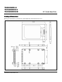
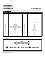
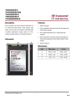
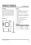
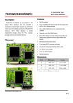
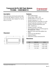
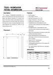
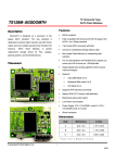
TTS
S88G
GS
SS
SD
D2255--S
S
TTS
S1166G
GS
SS
SD
D2255--S
S
TTS
S3322G
GS
SS
SD
D2255--M
M
2.5” Solid State Disk
Description
Features
Due to smaller size (fit the standard dimensions of
•
RoHS compliant
2.5” IDE Hard Disk Drives), huge capacity, high
•
Fully compatible with devices and OS that support the
speed, and low power consumption, Solid State Disk
IDE standard (44-Pin, pitch = 2.00 mm)
is perfect replacement storage device for PCs,
•
Laptops, gaming systems, and handheld devices.
•
Placement
Non-volatile Flash Memory for outstanding data
retention
Built-in ECC (Error Correction Code) functionality and
wear-leveling algorithm ensures highly reliable of data
transfer
•
Supports up to Ultra DMA Mode 4
•
Lower Power Consumption
•
Shock resistance
Dimensions
Transcend Information Inc.
1
Side
Millimeters
Inches
A
100.00 ± 0.40
3.937 ± 0.016
B
69.85 ± 0.20
2.750 ± 0.008
C
7.40 ± 0.15
0.291 ± 0.004
TTS
S88G
GS
SS
SD
D2255--S
S
TTS
S1166G
GS
SS
SD
D2255--S
S
TTS
S3322G
GS
SS
SD
D2255--M
M
2.5” Solid State Disk
Specifications
Physical Specification
Form Factor
2.5-inch HDD
Storage Capacities
8 GB to 32 GB
Dimensions (mm)
Length
100.0 0 ± 0.40
Width
69.85 ± 0.20
Height
7.40 ± 0.15
Input Voltage
5V ± 5%
Weight
80 g
Connector
44-Pin standard IDE/ATA connector (Pitch 2.0 mm)
Environmental Specifications
Operating Temperature
0 ℃ to 70 ℃
Storage Temperature
- 40 ℃ to 85 ℃
Reliability
Data Reliability
Built-in 4 symbol/page correction ECC
Data Retention
10 years
Connector Durability
10,000 times
Interface Specification
Jumper Settings
Master/Slave/Cable-select Settings
Drivers
No Device Driver Required
ATA/ATAPI 5
ATA Compatibility
UDMA Modes 0 - 4
Compliance and Warranty
Compliance
CE, FCC and BSMI
Warranty
2 years
Transcend Information Inc.
2
TTS
S88G
GS
SS
SD
D2255--S
S
TTS
S1166G
GS
SS
SD
D2255--S
S
TTS
S3322G
GS
SS
SD
D2255--M
M
2.5” Solid State Disk
Package Dimensions
Below figure illustrates the Transcend 2.5” Solid State Disk. All dimensions are in mm.
Transcend Information Inc.
3
TTS
S88G
GS
SS
SD
D2255--S
S
TTS
S1166G
GS
SS
SD
D2255--S
S
TTS
S3322G
GS
SS
SD
D2255--M
M
2.5” Solid State Disk
Pin Assignments
Pin No.
Pin Name
Pin No.
Pin Name
01
03
05
07
-RESET
DD7
DD6
DD5
02
04
06
08
GND
DD8
DD9
DD10
09
11
13
15
17
19
21
23
DD4
DD3
DD2
DD1
DD0
GND
DMARQ
-DIOW : STOP
10
12
14
16
18
20
22
24
DD11
DD12
DD13
DD14
DD15
KEY-PIN (OPEN)
GND
GND
25
27
29
31
33
35
37
39
-DIOR : -HDMARDY : HSTROBE
IORDY : DDMARDY : DSTROBE
-DMACK
INTRQ
DA1
DA0
-CS0
-DASP
26
28
30
32
34
36
38
40
GND
CSEL
GND
IOCS16B
-PDIAG : -CBLID
DA2
-CS1
GND
41
43
VCC
GND
42
44
VCC
NC (No Connect)
Pin Layout
Transcend Information Inc.
4
TTS
S88G
GS
SS
SD
D2255--S
S
TTS
S1166G
GS
SS
SD
D2255--S
S
TTS
S3322G
GS
SS
SD
D2255--M
M
2.5” Solid State Disk
Pin Description
Pin No.
Signal
01
-RESET
17, 15, 13, 11, 09, 07,
05, 03, 04, 06, 08, 10,
12, 14, 16, 18
DD0 ~ DD15 (Device Data)
21
DMARQ (DMA Request)
I/O*
I
Hardware reset signal from the host.
I/O
O
23
-DIOW (I/O Write)
STOP (Stop UDMA Burst)
25
I
For DMA data transfers. Device will assert DMARQ
when the device is ready to transfer data to or from the
host.
The host asserts this signal during an UDMA burst to
stop the DMA burst.
-DIOR (I/O Read)
This is the strobe signal used by the host to read from
the device register or the Data port.
When UDMA mode DMA Read is ready, -HDMARDY
should be asserted by the host to indicate that the host is
ready to receive DMA data-in burst.
I
HSTROBE (UDMA Strobe)
HSTROBE receives the data-out strobe signal from the
host for an UDMA burst.
IORDY (I/O channel ready)
This signal is used to temporarily stop the host register
access (read or write) when the device is not ready to
respond to a data transfer request.
DDMARDY (UDMA ready)
28
16-bit bi-direction Data Bus. DD(7:0) are used for 8-bit
register transfers.
This is the strobe signal used by the host to write to the
device register or Data port.
-HDMARDY (UDMA ready)
27
Description
O
The device will assert this signal to indicate that the
device is ready to receive UDMA data-out burst.
DSTROBE (UDMA data
strobe)
When UDMA mode DMA Read is active, this signal is
the data-in strobe generated by the device.
CSEL (Cable select)
I
This pin is used to configure this device as Device 0 or
Device 1. When this pin is grounded, this device is
configured as Device 0. When this pin is High, this
device is configured as Device 1.
I
This signal is used by the host in response to DMARQ to
initiate DMA transfer.
O
When this device is selected, this signal is the active
high Interrupt Request to the host.
29
-DMACK (DMA
acknowledge)
31
INTRQ (Interrupt)
Transcend Information Inc.
5
TTS
S88G
GS
SS
SD
D2255--S
S
TTS
S1166G
GS
SS
SD
D2255--S
S
TTS
S3322G
GS
SS
SD
D2255--M
M
32
2.5” Solid State Disk
IOCS16B
O
35, 33, 36
DA0 ~ DA2 (Device
Address)
34
-PDIAG (Passed
diagnostics)
-CBLID (Cable assembly
type identifier)
37, 38
This is the 3-bit binary coded Address Bus.
I
I/O
-CS0, -CS1 (Chip select)
39
-DASP (Device active,
Device 1 present)
41, 42
VCC
2, 19, 22, 24, 26, 30,
40, 43
GND
During PIO transfer mode 0, 1 or 2, this pin indicates to
the host the 16-bit data port has been addressed and the
device is prepared to send or receive a 16-bit data word.
When transferring in PIO mode 3, 4, or above, this signal
should not be used by the host, and all transfers will be
16-bit. When transferring in DMA mode, the host must
use a 16-bit DMA channel and this signal will not be
asserted.
This signal will be asserted by Device 1 to indicate to
Device 0 that Device 1 has completed diagnostics.
I
These signals are used to select the Command Block
and Control Block registers. When –DMACK is asserted,
-CS0 and –CS1 shall be negated and transfers shall be
16-bit wide.
I/O
During the reset protocol, -DASP shall be asserted by
Device 1 to indicate that the device is present.
P
Power supply.
Ground.
-
* Note:
“I”
An input from the host system to the device.
“O”
An output from the device to the host system.
“I/O”
An input/output (bi-direction) common.
“P”
Power supply.
Transcend Information Inc.
6
TTS
S88G
GS
SS
SD
D2255--S
S
TTS
S1166G
GS
SS
SD
D2255--S
S
TTS
S3322G
GS
SS
SD
D2255--M
M
2.5” Solid State Disk
Block Diagram
Data bus
44 PIN IDE Connector
Control
Signal
D00 ~ D07
Flash Memory
-CE0, -CE2…
D0 – D7
-CE0
-CE1
-WE…-RE
Others
IDE
Power
Flash Disk
Controller
Flash Memory
D10 ~ D17
D0 – D7
-CE0
-CE1
-WE…-RE
-CE1, -CE3…
DC Characteristics
Symbol
IoL
IoLDASP
IoH
IoHDMARQ
IZ
ViH
ViL
VoH
VoL
Description
Driver sink current
Driver sink current for DASP
Driver source current
Driver source current for DMARQ
Device pull-up current on DD(15:0) and
STROBE when released
Voltage input high
Voltage input low
Voltage output high at IoH min
Voltage output low at IoL min
Min
4
12
400
500
-10
Max
2.0
5.5
0.8
200
Units
mA
mA
µA
µA
µA
0.5
V
V
V
V
Max
1.25
1.25
25
Units
V/ns
V/ns
pf
20
pf
2.4
AC Characteristics
Symbol
SRISE
SFALL
Chost
Cdevice
Description
Rising edge slew rate for any signal
Falling edge slew rate for any signal
Host interface signal capacitance at the
host connector
Device interface signal capacitance at
the device connector
Transcend Information Inc.
7
Min
TTS
S88G
GS
SS
SD
D2255--S
S
TTS
S1166G
GS
SS
SD
D2255--S
S
TTS
S3322G
GS
SS
SD
D2255--M
M
2.5” Solid State Disk
Ordering Information
-S = SLC
-M = MLC
Form Factor:
25 = 2.5"
18 = 1.8"
10 = 1.0"
Transcend Product
Capacity:
8GB up to 32GB
Solid State Disk
The above technical information is based on industry standard data and has been tested to be reliable. However,
Transcend makes no warranty, either expressed or implied, as to its accuracy and assumes no liability in connection with
the use of this product. Transcend reserves the right to make changes to the specifications at any time without prior notice.
USA
Los Angeles:
E-mail: [email protected]
Maryland:
E-mail: [email protected]
www.transcendusa.com
CHINA
E-mail: [email protected]
www.transcendchina.com
TAIWAN
No.70, XingZhong Rd., NeiHu Dist., Taipei, Taiwan, R.O.C
TEL +886-2-2792-8000
Fax +886-2-2793-2222
E-mail: [email protected]
www.transcend.com.tw
GERMANY
E-mail: [email protected]
www.transcend.de
HONG KONG
E-mail: [email protected]
www.transcendchina.com
JAPAN
E-mail: [email protected]
www.transcend.jp
THE NETHERLANDS
E-mail: [email protected]
www.transcend.nl
United Kingdom
E-mail: [email protected]
www.transcend-uk.com
Transcend Information Inc.
8