1
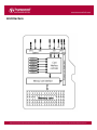
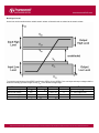
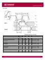
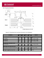
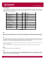
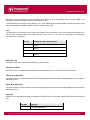
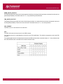
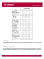
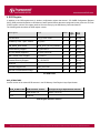
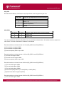
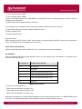
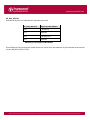
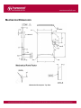
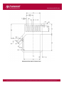
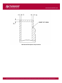
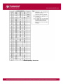
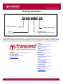
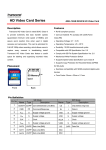
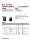
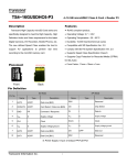
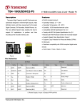
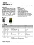
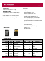
USDC10I – Industrial High Capacity microSD Card Transcend industrial USDC10I microSDHC cards are manufactured with high quality industrial controller and MLC NAND Flash chips. Transcend industrial SDHC10I microSDHC cards can provide high performance and excellent reliability. Features RoHS compliant Operating Voltage: 2.7 ~ 3.6V Operating Temperature: -40 ~ 85°C Durability: 10,000 insertion/removal cycles Compatible with SD Specification Ver. 3.0 SD File System Specification Ver. 3.0 compliant Supports Speed Class Specification Class 10 Supports Copy Protection for Recorded Media (CPRM) for SD-Audio Placement 12345678 Form Factor: 11mm x 15mm x 1mm Power cycle robustness Electrostatic protection (ICE 61000-4-2) Waterproof (IPX7) MLC NAND solution Pin Definition SD Mode SPI Mode Pin No. Name Type Description Name Type 1 DAT2 I/O/PP Data Line [Bit2] 2 CD/DAT3 I/O/PP Card Detect / Data Line [Bit3] CS I Chip Select 3 CMD PP Command / Response DI I Data In 4 VDD S Supply voltage VDD S Supply voltage 5 CLK I Clock SCLK I Clock 6 VSS S Supply voltage ground VSS S Supply voltage ground 7 DAT0 I/O/PP Data Line [Bit0] DO O/PP 8 DAT1 I/O/PP Data Line [Bit1] RSV RSV Description Reserved Data out Reserved Architecture Bus Operating Conditions General Parameter Symbol Min. Max. Unit -0.3 VDD+0.3 V -10 10 µA -10 10 µA Symbol Min. Max. Unit Supply voltage VDD 2.7 3.6 V Output High Voltage VOH 0.75* VDD Output Low Voltage VOL Input High Voltage VIH Input Low Voltage VIL Peak voltage on all lines Remark All Inputs Input Leakage Current All Outputs Output Leakage Current Power Supply Voltage Parameter 0.125* VDD 0.625* VDD VDD+0.3 VSS-0.3 • Operation in Default Mode: Maximum 100 mA • Operation in High Speed Mode: Maximum 200 mA • Operation with other functions: Maximum 500 mA V IOL=100uA@VDD Min. V 250 ms The current consumption is measured by averaging over 1 second. • During initialization: Maximum 100 mA IOH=-100uA@VDD Min. V Current Consumption • Before first command: Maximum 15 mA V 0.25* VDD Power up time Remark From 0v to VDD Min. Bus Signal Line Load The total capacitance CL the CLK line of the SD Memory Card bus is the sum of the bus master capacitance CHOST, the bus capacitance CBUS itself and the capacitance CCARD of each card connected to this line: CL = CHOST + CBUS + *CCARD Where N is the number of connected cards. Parameter Pull-up resistance Symbol Min. Max. Unit Remark RCMD 10 100 k To prevent bus floating 40 pF 1 card RDAT Bus signal line capacitance CL CHOST+CBUS shall not exceed 30 pF Single card capacitance CCARD Pull-up resistance inside card (pin1) RDAT3 Capacity Connected to Power Line CC 10 10 pF 90 k May be used for card detection 5 uF To prevent inrush current Note that the total capacitance of CMD and DAT lines will be consist of C HOST, CBUS and one CCARD only because they are connected separately to the SD Memory Card host. Host should consider total bus capacitance for each signal as the sum of C HOST, CBUS, and CCARD, these parameters are defined by per signal. The host can determine CHOST and CBUS so that total bus capacitance is less than the card estimated capacitance load (CL=40 pF). The SD Memory Card guarantees its bus timing when total bus capacitance is less than maximum value of CL (40 pF) Bus Signal Levels As the bus can be supplied with a variable supply voltage, all signal levels are related to the supply voltage. To meet the requirements of the JEDEC specification JESD8-1A and JESD8-7, the card input and output voltages shall be within the following specified ranges for any VDD of the allowed voltage range: Parameter Symbol Min. Output HIGH voltage VOH 0.75* VDD Output LOW voltage VOL Input HIGH voltage VIH 0.625* VDD Input LOW voltage VIL VSS – 0.3 Max. Unit Remark V IOH = -100 μA @VDD min 0.125* VDD V IOL = -100 μA @VDD min VDD + 0.3 V 0.25* VDD V Bus Timing Parameter Symbol Min Max. Unit Remark Clock CLK (All values are referred to min (VIH) and max (VIL) Clock frequency Data Transfer Mode fPP 0 25 MHz CCARD 10 pF, (1 card) Clock frequency Identification Mode fOD 0(1)/100 400 KHz CCARD 10 pF, (1 card) Clock low time tWL 10 ns CCARD 10 pF, (1 card) Clock high time tWH 10 ns CCARD 10 pF, (1 card) Clock rise time tTLH 10 ns CCARD 10 pF, (1 card) Clock fall time tTHL 10 ns CCARD 10 pF, (1 card) Inputs CMD, DAT (referenced to CLK) Input set-up time tISU 5 ns CCARD 10 pF, (1 card) Input hold time tIH 5 ns CCARD 10 pF, (1 card) tODLY 0 ns CL 40 pF, (1 card) Outputs CMD, DAT (referenced to CLK) Output Delay time during Data Transfer Mode 14 Output Delay time during Identification Mode tODLY 0 50 ns CL 40 pF, (1 card) (1) 0 Hz means to stop the clock. The given minimum frequency range is for cases were continues clock is required Bus Timing (High Speed Mode) Parameter Symbol Min Max. Unit Remark 50 MHz CCARD 10 pF, (1 card) ns CCARD 10 pF, (1 card) Clock CLK (All values are referred to min (VIH) and max (VIL) Clock frequency Data Transfer Mode fPP 0 Clock low time tWL 7 Clock high time tWH 7 ns CCARD 10 pF, (1 card) Clock rise time tTLH 3 ns CCARD 10 pF, (1 card) Clock fall time tTHL 3 ns CCARD 10 pF, (1 card) Inputs CMD, DAT (referenced to CLK) Input set-up time tISU 6 ns CCARD 10 pF, (1 card) Input hold time tIH 2 ns CCARD 10 pF, (1 card) 14 ns CL 40 pF, (1 card) ns CL 40 pF, (1 card) 40 pF (1 card) Outputs CMD, DAT (referenced to CLK) Output Delay time during Data Transfer Mode Output Hold time tODLY tOH 1 2.5 Total System capacitance for each line CL 1) In order to satisfy severe timing, host shall drive only one card. Reliability and Durability Temperature Operation: -40°C / 85°C Storage: -40°C (168h) / 85°C (500h) Junction temperature: max. 95°C Moisture and corrosion Operation: 25°C / 95% rel. humidity Storage: 40°C / 93% rel. hum./500h Salt Water Spray: 3% NaCl/35C; 24h acc. MIL STD Method 1009 Durability 10.000 mating cycles; Drop test 1.5m free fall UV light exposure UV: 254nm, 15Ws/cm² according to ISO 7816-1 Shock IEC 60512-6-3 acceleration 490 m/s ESD IEC 61000-4-2 Water proof JIS IPX7 2 Register Information Within the card interface six registers are defined: OCR, CID, CSD, RCA, DSR and SCR. These can be accessed only by corresponding commands. The OCR, CID, CSD and SCR registers carry the card/content specific information, while the RCA and DSR registers are configuration registers storing actual configuration parameters. 1. OCR register The 32-bit operation conditions register stores the VDD voltage profile of the card. Additionally, this register includes status information bits. One status bit is set if the card power up procedure has been finished. This register includes another status bit indicating the card capacity status after set power up status bit. The OCR register shall be implemented by the cards. The 32-bit operation conditions register stores the VDD voltage profile of the card. Bit 7 of OCR is newly defined for Dual Voltage Card and set to 0 in default. If a Dual Voltage Card does not receive CMD8, OCR bit 7 in the response indicates 0, and the Dual Voltage Card which received CMD8, sets this bit to 1. Additionally, this register includes 2 more status information bits. Bit 31 - Card power up status bit, this status bit is set if the card power up procedure has been finished. Bit 30 - Card capacity status bit, this status bit is set to 1 if card is High Capacity SD Memory Card. 0 indicates that the card is Standard Capacity SD Memory Card. The Card Capacity status bit is valid after the card power up procedure is completed and the card power up status bit is set to 1. The Host shall read this status bit to identify a Standard or High Capacity SD Memory Card. The OCR register shall be implemented by the cards. OCR Register Definition 1) This bit is valid only when the card power up status bit is set. 2) This bit is set to LOW if the card has not finished the power up routine. A voltage range is not supported if the corresponding bit value is set to LOW. As long as the card is busy, the corresponding bit (31) is set to LOW. 2. CID Register The Card Identification (CID) register is 128 bits wide. It contains the card identification information used during the card identification phase. Every individual flash card shall have a unique identification number. The structure of the CID register is defined in the following paragraphs: Name Field Width CID-slice Manufacturer ID MID 8 [127:120] OEM/Application ID OID 16 [119:104] Product name PNM 40 [103:64] Product revision PRV 8 [63:56] Product serial number PSN 32 [55:24] reserved -- 4 [23:20] Manufacturing date MDT 12 [19:8] CRC7 checksum CRC 7 [7:1] not used, always 1 - 1 [0:0] The CID Fields MID An 8-bit binary number that identifies the card manufacturer. The MID number is controlled, defined, and allocated to a SD Memory Card manufacturer by the SD-3C, LLC. This procedure is established to ensure uniqueness of the CID register. OID A 2-character ASCII string that identifies the card OEM and/or the card contents (when used as a distribution media either on ROM or FLASH cards). The OID number is controlled, defined, and allocated to a SD Memory Card manufacturer by the SD-3C, LLC. This procedure is established to ensure uniqueness of the CID register. Note: SD-3C, LLC licenses companies that wish to manufacture and/or sell SD Memory Cards, including but not limited to flash memory, ROM, OTP, RAM, and SDIO Combo Cards. SD-3C, LLC is a limited liability company established by Matsushita Electric Industrial Co. Ltd., SanDisk Corporation and Toshiba Corporation. PNM The product name is a string, 5 ASCII characters long. PRV The product revision is composed of two Binary Coded Decimal (BCD) digits, four bits each, representing an “n.m” revision number. The “n” is the most significant nibble and “m” is the least significant nibble. As an example, the PRV binary value field for product revision “6.2” will be: 0110 0010b PSN The Serial Number is 32 bits of binary number. MDT The manufacturing date composed of two hexadecimal digits, one is 8 bit representing the year(y) and the other is four bits representing the month(m). The “m” field [11:8] is the month code. 1 = January. The “y” field [19:12] is the year code. 0 = 2000. As an example, the binary value of the Date field for production date “April 2001” will be: 00000001 0100. CRC CRC7 checksum (7 bits). 3. CSD Register The CSD Regsiter shows Definition of the CSD for the High Capacity SD Memory Card and Extended Capacity SD Memory Card (CSD Version 2.0). The following sections describe the CSD fields and the relevant data types for the High Capacity SD Memory Card. CSD Version 2.0 is applied to SDHC and SDXC Cards. The field name in parenthesis is set to fixed value and indicates that the host is not necessary to refer these fields. The fixed values enables host,which refers to these fields, to keep compatibility to CSD Version 1.0. The Cell Type field is coded as follows: R = readable, W(1) = writable once, W = multiple writable. Name Field Width Value Cell Type CSD-slice CSD structure CSD_STRUCTURE 2 01b R [127:126] reserved - 6 00 0000b R [125:120] data read access-time (TAAC) 8 0Eh R [119:112] data read access-time in CLK (NSAC) 8 00h R [111:104] cycles (NSAC*100) max. data transfer rate (TRAN_SPEED) 8 32h, 5Ah, 0Bh or 2Bh R [103:96] card command classes* CCC 12 01x110110101b R [95:84] max. read data block length** (READ_BL_LEN) 4 9 R [83:80] 1 0 R [79:79] write block misalignment** (WRITE_BLK_MISALIGN) 1 0 R [78:78] read block misalignment** (READ_BLK_MISALIGN) 1 0 R [77:77] DSR implemented** DSR_IMP 1 x R [76:76] reserved - 6 00 0000b R [75:70] partial blocks for read allowed** (READ_BL_PARTIAL) device size*** C_SIZE 22 xxxxxxh R [69:48] reserved - 1 0 R [47:47] erase single block enable** (ERASE_BLK_EN) 1 1 R [46:46] erase sector size** (SECTOR_SIZE) 7 7Fh R [45:39] write protect group size** (WP_GRP_SIZE) 7 0000000b R [38:32] write protect group enable** (WP_GRP_ENABLE) 1 0 R [31:31] 2 00b R [30:29] reserved write speed factor** (R2W_FACTOR) 3 010b R [28:26] max. write data block length** (WRITE_BL_LEN) 4 9 R [25:22] partial blocks for write allowed** (WRITE_BL_PARTIAL) 1 0 R [21:21] reserved - 5 00000b R [20:16] File format group** (FILE_FORMAT_GRP) 1 0 R [15:15] copy flag COPY 1 x R/W(1) [14:14] permanent write protection PERM_WRITE_PROTECT 1 x R/W(1) [13:13] temporary write protection TMP_WRITE_PROTECT 1 x R/W [12:12] File format** (FILE_FORMAT) 2 00b R [11:10] reserved - 2 00b R [9:8] CRC CRC 7 xxxxxxxb R/W [7:1] not used, always'1' - 1 1 - [0:0] The CSD Register Fields (CSD Version 2.0) The following sections describe the CSD fields and the relevant data types. If not explicitly defined otherwise, all bit strings are interpreted as binary coded numbers starting with the left bit first. CSD_STRUCTURE Field structures of the CSD register are different depend on the Physical Specification Version and Card Capacity. The CSD_STRUCTURE field in the CSD register indicates its structure version. The following table shows the version number of the related CSD structure. CSD_STRUCTURE CSD structure version Card Capacity 0 CSD Version 1.0 Standard Capacity 1 CSD Version 2.0 High Capacity and Extended Capacity 2-3 reserved CSD Register Structure TAAC This field is fixed to 0Eh, which indicates 1 ms. The host should not use TAAC, NSAC, and R2W_FACTOR to calculate timeout and should uses fixed timeout values for read and write operations. TAAC bit position code 2:0 time unit 0=1ns, 1=10ns, 2=100ns, 3=1µs, 4=10µs, 5=100µs, 6=1ms, 7=10ms 6:3 time value 0=reserved, 1=1.0, 2=1.2, 3=1.3, 4=1.5, 5=2.0, 6=2.5, 7=3.0, 8=3.5, 9=4.0, A=4.5, B=5.0, C=5.5, D=6.0, E=7.0, F=8.0 7 reserved NSAC This field is fixed to 00h. NSAC should not be used to calculate time-out values. TRAN_SPEED The following table defines the maximum data transfer rate per one data line - TRAN_SPEED: TRAN_SPEED bit code 2:0 transfer rate unit 0=100kbit/s, 1=1Mbit/s, 2=10Mbit/s, 3=100Mbit/s, 4... 7=reserved 6:3 time value 0=reserved, 1=1.0, 2=1.2, 3=1.3, 4=1.5, 5=2.0, 6=2.5, 7=3.0, 8=3.5, 9=4.0, A=4.5, B=5.0, C=5.5, D=6.0, E=7.0, F=8.0 7 reserved Note that for current SD Memory Cards that field must be always 0_0110_010b (032h) which is equal to 25MHz - the mandatory maximum operating frequency of SD Memory Card. In High-Speed mode, that field must be always 0_1011_010b (05Ah) which is equal to 50MHz. And when the timing mode returns to the default by CMD6 or CMD0 command, its value will be 032h. CCC The SD Memory Card command set is divided into subsets (command classes). The card command class register CCC defines which command classes are supported by this card. A value of ‘1’ in a CCC bit means that the corresponding command class is supported. CCC bit Supported card command class 0 class 0 1 class 1 ...... 11 class 11 READ_BL_LEN This field is fixed to 9h, which indicates READ_BL_LEN=512 Byte. READ_BL_PARTIAL This field is fixed to 0, which indicates partial block read is inhibited and only unit of block access is allowed. WRITE_BLK_MISALIGN This field is fixed to 0, which indicates write access crossing physical block boundaries is always disabled in High Capacity SD Memory Card. READ_BLK_MISALIGN This field is fixed to 0, which indicates read access crossing physical block boundaries is always disabled in High Capacity SD Memory Card. DSR_IMP Defines if the configurable driver stage is integrated on the card. If set, a driver stage register (DSR) must be implemented also. DSR_IMP DSR type 0 no DSR implemented 1 DSR implemented C_SIZE This field is expanded to 22 bits and can indicate up to 2 TBytes (It is the same as the maximum memory space specified by a 32-bit block address.) This parameter is used to calculate the user data area capacity in the SD memory card (not include the protected area). The user data area capacity is calculated from C_SIZE as follows: memory capacity = (C_SIZE+1) * 512K byte As the maximum capacity of the Physical Layer Specification Version 2.00 is 32 GB, the upper 6 bits of this field shall be set to 0. ERASE_BLK_EN This field is fixed to 1, which means the host can erase one or multiple units of 512 bytes. SECTOR_SIZE This field is fixed to 7Fh, which indicates 64 KBytes. This value does not relate to erase operation. Version 2.00 cards indicates memory boundary by AU size and this field should not be used. WP_GRP_SIZE This field is fixed to 00h. The High Capacity SD Memory Card does not support write protected groups. WP_GRP_ENABLE This field is fixed to 0. The High Capacity SD Memory Card does not support write protected groups. R2W_FACTOR This field is fixed to 2h, which indicates 4 multiples. Write timeout can be calculated by multiplying the read access time and R2W_FACTOR. However, the host should not use this factor and should use 250 ms for write timeout. WRITE_BL_LEN This field is fixed to 9h, which indicates WRITE_BL_LEN=512 Byte. WRITE_BL_PARTIAL This field is fixed to 0, which indicates partial block read is inhibited and only unit of block access is allowed. FILE_FORMAT_GRP This field is set to 0. Host should not use this field. COPY Defines if the contents is original (= ‘0’) or has been copied (=’1’). The COPY bit for OTP and MTP devices, sold to end consumers, is set to ‘1’ which identifies the card contents as a copy. The COPY bit is an one time programmable bit. PERM_WRITE_PROTECT Permanently protects the whole card content against overwriting or erasing (all write and erase commands for this card are permanently disabled). The default value is ‘0’, i.e. not permanently write protected. TMP_WRITE_PROTECT Temporarily protects the whole card content from being overwritten or erased (all write and erase commands for this card are temporarily disabled). This bit can be set and reset. The default value is ‘0’, i.e. not write protected. FILE_FORMAT This field is set to 0. Host should not use this field. CRC The CRC field carries the check sum for the CSD contents. The checksum has to be recalculated by the host for any CSD modification. The default corresponds to the initial CSD contents. The following table lists the correspondence between the CSD entries and the command classes. A ‘+’ entry indicates that the CSD field affects the commands of the related command class. 4. RCA Register The writable 16-bit relative card address register carries the card address that is published by the card during the card identification. This address is used for the addressed host-card communication after the card identification procedure. The default value of the RCA register is 0x0000. The value0x0000 is reserved to set all cards into the Stand-by State with CMD7. 5. DSR Register (Optional) It can be optionally used to improve the bus performance for extended operating conditions (depending on parameters like bus length, transfer rate or number of cards). The CSD register carries the information about the DSR register usage. The default value of the DSR register is 0x404. 6. SCR Register In addition to the CSD register there is another configuration register that named - SD CARD Configuration Register (SCR). SCR provides information on SD Memory Card's special features that were configured into the given card. The size of SCR register is 64 bit. This register shall be set in the factory by the SD Memory Card manufacturer. The following table describes the SCR register content. Description Field Width Cell Type SCR Slice SCR Structure SCR_STRUCTURE 4 R [63:60] SD Memory Card - Spec. Version SD_SPEC 4 R [59:56] data_status_after erases DATA_STAT_AFTER_ERASE 1 R [55] CPRM Security Support SD_SECURITY 3 R [54:52] DAT Bus widths supported SD_BUS_WIDTHS 4 R [51:48] Spec. Version 3.00 or higher SD_SPEC3 1 R [47] Extended Security Support EX_ SECURITY 4 R [46:43] Reserved - 9 R [42:34] Command Support bits CMD_SUPPORT 2 R [33:32] reserved for manufacturer usage - 32 R [31:0] The SCR Fields SCR_STRUCTURE Version number of the related SCR structure in the SD Memory Card Physical Layer Specification. SCR_STRUCTURE SCR structure version SD Physical Layer Specification Version 0 SCR version 1.0 Version 1.01-3.00 1-15 reserved SCR Register Structure Version SD_SPEC Describes the SD Memory Card Physical Layer Specification version supported by this card. SD_SPEC 0 1 Physical Layer Specification Version Number Version 1.0-1.01 Version 1.10 Version 2.00 or Version 3.00 (Refer to SD_SPEC3) reserved 2 3-15 Physical Layer Specification Version SD_SPEC3 SD_SPEC SD_SPEC3 Physical Layer Specification Version Number 2 0 Version 2.00 2 1 Version 3.00 The card manufacturer determines SD_SPEC value by conditions indicated below. All conditions shall be satisfied for each version. The other combination of conditions is not allowed. Essential conditions to indicate Version 1.01 Card (SD_SPEC=0 and SD_SPEC3=0) (1)The card does not support CMD6 (2)The card does not support CMD8 (3) User area capacity shall be up to 2GB Essential conditions to indicate Version 1.10 Card (SD_SPEC=1 and SD_SPEC3=0) (1) The card shall support CMD6 (2) The card does not support CMD8 (3) User area capacity shall be up to 2GB Essential conditions to indicate Version 2.00 Card (SD_SPEC=2 and SD_SPEC3=0) (1) The card shall support CMD6 (2) The card shall support CMD8 (3) The card shall support CMD42 (4) User area capacity shall be up to 2GB (SDSC) or 32GB (SDHC) (5) Speed Class shall be supported (SDHC) Essential conditions to indicate Version 3.00 Card (SD_SPEC=2 and SD_SPEC3=1) (1) The card shall support CMD6 (2) The card shall support CMD8 (3) The card shall support CMD42 (4) User area capacity shall be up to 2GB (SDSC) or 32GB (SDHC) User area capacity shall be more than or equal to 32GB and up to 2TB (SDXC) (5) Speed Class shall be supported (SDHC or SDXC) A card supports any of following functions shall satisfy essential conditions of Version 3.00 Card (1) Speed Class supported under the conditions defined in Ver3.00 (2) UHS-I supported card (3) CMD23 supported card Application Notes: When checking SD_SPEC version in SCR, the host shall not forget that higher SD_SPEC version may be specified in future. It is important to keep compatibility for future version. DATA_STAT_AFTER_ERASE Defines the data status after erase, whether it is ‘0’ or ‘1’ (the status is card vendor dependent). SD_SECURITY This field indicates CPRM Security Specification Version for each capacity card. The definition of Protected Area is different in each capacity card. SD_SECURITY CPRM Security Version 0 No Security 1 Not Used 2 SDSC Card (Security Version 1.01) 3 SDHC Card (Security Version 2.00) 4 SDXC Card (Security Version 3.xx) 5-7 Reserved CPRM Security Version The basic rule of setting this field: SDSC Card sets this field to 2 (Version 1.01) SDHC Card sets this field to 3 (Version 2.00). SDXC Card sets this field to 4 (Version 3.xx). Note that it is mandatory for a regular writable SD Memory Card to support Security Protocol. For ROM (Read Only) and OTP (One Time Programmable) types of the SD Memory Card, the security feature is optional. SD_BUS_WIDTHS Describes all the DAT bus widths that are supported by this card. SD_BUS_WIDTHS Supported Bus Widths Bit 0 1 bit (DAT0) Bit 1 reserved Bit 2 4 bit (DAT0-3) Bit 3 reserved SD Memory Card Supported Bus Widths Since SD Memory Card shall support at least the two bus modes 1bit or 4bit width then any SD Card shall set at least bits 0 and 2 (SD_BUS_WIDTH="0101"). Mechanical Dimension Mechanical Description: Top View Mechanical Description: Bottom View Mechanical Description: Keep Out Area microSD package: Dimensions Ordering Information TS XG USDC 10I Transcend Product Class 10 Industrial Card Capacity 8GB - 32GB MicorSDHC Card Micro High Capacity Secure Digital Card The technical information above is based on commercial standard data and has been tested to be reliable. However, Transcend makes no warranty, either expressed or implied, as to its accuracy and assumes no liability in connection with the use of this product. Transcend reserves the right to make changes to the specifications at any time without prior notice. USA Los Angeles: E-mail: [email protected] Maryland: E-mail: [email protected] www.transcend-info.com CHINA E-mail: [email protected] cn.transcend-info.com TAIWAN GERMANY No.70, XingZhong Rd., NeiHu Dist., Taipei, Taiwan, R.O.C TEL +886-2-2792-8000 Fax +886-2-2793-2222 E-mail: [email protected] tw.transcend-info.com E-mail: [email protected] de.transcend-info.com HONG KONG E-mail: [email protected] hk.transcend-info.com JAPAN E-mail: [email protected] jp.transcend-info.com THE NETHERLANDS E-mail: [email protected] nl.transcend-info.com United Kingdom E-mail: [email protected] uk.transcend-info.com KOREA E-mail: [email protected] kr.transcend-info.com Version Date V1.0 2015/02/26 Revision History Modification Content Formal release Modified Page