1
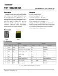
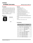
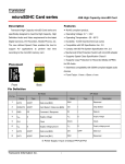
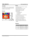
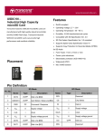
T
TS
S22G
GU
US
SD
D--P
P33
2GB microSD Card + Reader P3
Description
Features
• ROHS compliant product.
Transcend microSD card series are non-volatile,
which means no external power is required to retain
• Operating Voltage: 2.7 ~ 3.6V
the information stored on it. Besides, it is also a
• Operating Temperature: -25 ~ 85°C
solid-state device that without moving parts to skip or
• Durability: 10,000 insertion/removal cycles
break down. Based on original NAND flash chip,
• Fully compatible with SD card spec. v1.1
Transcend
• Comply with SD Association File System Specification
microSD
can
offer
an
incredible
combination of fast data transfer, great flexibility,
• Mechanical Write Protection Switch with microSD adapter
excellent security and incredibly small size.
• SD Host allows MultiMediaCard upward compatibility
• Form Factor: 11mm x 15mm x 1mm
Placement
12345678
Front
Back
Pin Definition
SD Mode
SPI Mode
Pin No.
Name
Type
Description
Name
Type
Description
1
DAT2
I/O/PP
Data Line [Bit2]
RSV
Reserved
2
CD/DAT3
I/O/PP
Card Detect / Data Line [Bit3]
CS
I
Chip Select
3
CMD
PP
Command / Response
DI
I
Data In
4
VDD
S
Supply voltage
VDD
S
Supply voltage
5
CLK
I
Clock
SCLK
I
Clock
6
VSS
S
Supply voltage ground
VSS
S
Supply voltage ground
7
DAT0
I/O/PP
Data Line [Bit0]
DO
O/PP
Data out
8
DAT1
I/O/PP
Data Line [Bit1]
RSV
S: Power Supply; I:Input; O:Output; PP:Push-Pull
Transcend Information Inc.
1
Reserved
T
TS
S22G
GU
US
SD
D--P
P33
2GB microSD Card + Reader P3
Architecture
Transcend Information Inc.
2
T
TS
S22G
GU
US
SD
D--P
P33
2GB microSD Card + Reader P3
Bus Operating Conditions
• General
Parameter
Symbol
Min.
Max.
Unit
-0.3
VDD+0.3
V
-10
10
µA
-10
10
µA
Symbol
Min.
Max.
Unit
VDD
2.0
3.6
V
Peak voltage on all lines
Remark
All Inputs
Input Leakage Current
All Outputs
Output Leakage Current
• Power Supply Voltage
Parameter
Supply voltage
Supply voltage specified in OCR register
Remark
CMD0, 15,55,ACMD41
commands
Except CMD0, 15,55,
ACMD41 commands
Supply voltage differentials (VSS1, VSS2)
-0.3
Power up time
0.3
V
250
ms
From 0v to VDD Min.
Note. The current consumption of any card during the power-up procedure must not exceed 10 mA.
• Bus Signal Line Load
The total capacitance CL the CLK line of the SD Memory Card bus is the sum of the bus master capacitance CHOST, the bus
capacitance CBUS itself and the capacitance CCARD of each card connected to this line:
CL = CHOST + CBUS + Ν*CCARD
Where N is the number of connected cards. Requiring the sum of the host and bus capacitances not to exceed 30 pF for
up to 10 cards, and 40 pF for up to 30 cards, the following values must not be exceeded:
Parameter
Bus signal line capacitance
Single card capacitance
Symbol
Min.
Max.
Unit
CL
100
pF
CCARD
10
pF
16
nH
fPP ≤ 20 MHz
90
KΩ
May be used for card
detection
Maximum signal line inductance
Pull-up resistance inside card (pin1)
RDAT3
10
Remark
fPP ≤ 20 MHz, 7 cards
Note that the total capacitance of CMD and DAT lines will be consist of CHOST, CBUS and one CCARD only since they are
connected separately to the SD Memory Card host.
Parameter
Pull-up resistance
Bus signal line capacitance
Transcend Information Inc.
Symbol
Min.
Max.
Unit
RCMD, RDAT
10
100
KΩ
To prevent bus floating
250
pF
fPP ≤ 5 MHz, 21 cards
CL
3
Remark
T
TS
S22G
GU
US
SD
D--P
P33
2GB microSD Card + Reader P3
• Bus Signal Levels
As the bus can be supplied with a variable supply voltage, all signal levels are related to the supply voltage.
To meet the requirements of the JEDEC specification JESD8-1A, the card input and output voltages shall be within the
following specified ranges for any VDD of the allowed voltage range:
Parameter
Symbol
Min.
Output HIGH voltage
VOH
0.75* VDD
Output LOW voltage
VOL
Input HIGH voltage
VIH
Input LOW voltage
VIL
Transcend Information Inc.
Max.
Unit
Remark
V
IOH = -100 μA @VDD min
0.125* VDD
V
IOL = 100 μA @VDD min
0.625* VDD
VDD + 0.3
V
VSS – 0.3
0.25* VDD
V
4
T
TS
S22G
GU
US
SD
D--P
P33
2GB microSD Card + Reader P3
• Bus Timing
Parameter
Symbol
Min
Max.
Unit
Remark
Clock CLK (All values are referred to min (VIH) and max (VIL)
Clock frequency Data Transfer Mode
fPP
0
25
MHz
CL ≤ 100 pF, (7 cards)
Clock frequency Identification Mode
(The low freq. is required for MultiMediaCard
compatibility.)
fOD
0
400
KHz
CL ≤ 250 pF, (21 cards)
Clock low time
tWL
10
ns
CL ≤ 100 pF, (7 cards)
50
ns
CL ≤ 250 pF, (21 cards)
10
ns
CL ≤ 100 pF, (7 cards)
50
ns
CL ≤ 250 pF, (21 cards)
10
ns
CL ≤ 100 pF, (7 cards)
50
ns
CL ≤ 250 pF, (21 cards)
10
ns
CL ≤ 100 pF, (7 cards)
50
ns
CL ≤ 250 pF, (21 cards)
Clock high time
Clock rise time
Clock fall time
tWH
tTLH
tTHL
Inputs CMD, DAT (referenced to CLK)
Input set-up time
tISU
5
ns
CL ≤ 25 pF, (1 cards)
Input hold time
tIH
5
ns
CL ≤ 25 pF, (1 cards)
ns
CL ≤ 25 pF, (1 cards)
Outputs CMD, DAT (referenced to CLK)
Output Delay time
Transcend Information Inc.
tODLY
0
5
14
T
TS
S22G
GU
US
SD
D--P
P33
2GB microSD Card + Reader P3
Reliability and Durability
Temperature
Operation: -25°C / 85°C
Storage: -40°C (168h) / 85°C (500h)
Junction temperature: max. 95°C
Moisture and corrosion
Operation: 25°C / 95% rel. humidity
Storage: 40°C / 93% rel. hum./500h
Salt Water Spray: 3% NaCl/35C; 24h acc. MIL STD Method 1009
Durability
10000 mating cycles
Bending
10N
Torque
0.10N*m , +/- 2.5deg max
Drop test
1.5m free fall
UV light exposure
UV: 254nm, 15Ws/cm² according to ISO 7816-1
Visual inspection
Shape and form
No warppage; no mold skin; complete form; no cavities surface smoothness <= -0.1
mm/cm² within contour; no cracks; no pollution (fat, oil dust, etc.)
Above technical information is based on standard data and tested to be reliable. However, Transcend makes no warranty,
either expressed or implied, as to its accuracy and assumes no liability in connection with the use of this product.
Transcend reserves the right to make changes in specifications at any time without prior notice.
Transcend Information Inc.
6
T
TS
S22G
GU
US
SD
D--P
P33
2GB microSD Card + Reader P3
Register Information
Within the card interface six registers are defined: OCR, CID, CSD, RCA, DSR and SCR. These can be accessed only
by corresponding commands (see Chapter 4.7). The OCR, CID, CSD and SCR registers carry the card/content specific
information, while the RCA and DSR registers are configuration registers storing actual configuration parameters.
1. OCR register
The 32-bit operation conditions register stores the VDD voltage profile of the card. In addition, this
register includes a status information bit. This status bit is set if the card power up procedure has
been finished. The OCR register shall be implemented by the cards which do not support the full
operating voltage range of the SD Memory Card bus, or if the card power up extends the definition
in the timing diagram.
Transcend Information Inc.
7
T
TS
S22G
GU
US
SD
D--P
P33
2GB microSD Card + Reader P3
A voltage range is not supported if the corresponding bit value is set to LOW. As long as the card is busy, the
corresponding bit (31) is set to LOW.
2. CID Register
The Card IDentification (CID) register is 128 bits wide. It contains the card identification information used during the card
identification phase. Every individual flash card shall have a unique identification number. The structure of the CID
register is defined in the following paragraphs:
• MID
An 8 bit binary number that identifies the card manufacturer. The MID number is controlled, defined and allocated to a
SD Memory Card manufacturer by the SD Group. This procedure is established to ensure uniqueness of the CID
register.
• OID
A 2 ASCII string characters that identifies the card OEM and/or the card contents (when used as a distribution media
either on ROM or FLASH cards). The OID number is controlled, defined and allocated to a SD Memory Card
manufacturer by the SD Group. This procedure is established to ensure uniqueness of the CID register.
• PNM
The product name is a string, 5 ASCII characters long.
• PRV
The product revision is composed of two Binary Coded Decimal (BCD) digits, four bits each, representing an “n.m”
revision number. The “n” is the most significant nibble and “m” is the least significant nibble.
As an example, the PRV binary value field for product revision “6.2” will be: 0110 0010
• PSN
The Serial Number is 32 bits of binary number.
Transcend Information Inc.
8
T
TS
S22G
GU
US
SD
D--P
P33
2GB microSD Card + Reader P3
• MDT
The manufacturing date composed of two hexadecimal digits, one is 8 bit representing the year(y)
and the other is four bits representing the month(m).
The “m” field [11:8] is the month code. 1 = January.
The “y” field [19:12] is the year code. 0 = 2000.
As an example, the binary value of the Date field for production date “April 2001” will be:
00000001 0100.
• CRC
CRC7 checksum (7 bits).
3. CSD Register
The Card-Specific Data register provides information on how to access the card contents. The CSD defines the data
format, error correction type, maximum data access time, whether the DSR register can be used etc. The programmable
part of the register (entries marked by W or E, see below) can be changed by CMD27. The type of the entries in the table
below is coded as follows: R= readable, W(1) = writable once, W = multiple writable.
Transcend Information Inc.
9
T
TS
S22G
GU
US
SD
D--P
P33
2GB microSD Card + Reader P3
The following sections describe the CSD fields and the relevant data types. If not explicitly defined otherwise, all bit
strings are interpreted as binary coded numbers starting with the left bit first.
• CSD_STRUCTURE
Version number of the related CSD structure.
• TAAC
Defines the asynchronous part of the data access time.
Transcend Information Inc.
10
T
TS
S22G
GU
US
SD
D--P
P33
2GB microSD Card + Reader P3
• NSAC
Defines the worst case for the clock dependent factor of the data access time. The unit for NSAC is100 clock cycles.
Therefore, the maximal value for the clock dependent part of the data access time is 25.5k clock cycles.
The total access time NAC as expressed in the Table 34 is the sum of TAAC and NSAC. It has to be computed by the
host for the actual clock rate. The read access time should be interpreted as a typical delay for the first data bit of a data
block or stream.
• TRAN_SPEED
The following table defines the maximum data transfer rate per one data line - TRAN_SPEED:
Note that for current SD Memory Cards that field must be always 0_0110_010b (032h) which is equal to 25MHz - the
mandatory maximum operating frequency of SD Memory Card.
In High-Speed mode, that field must be always 0_1011_010b (05Ah) which is equal to 50MHz. And when the timing
mode returns to the default by CMD6 or CMD0 command, its value will be 032h.
• CCC
The SD Memory Card command set is divided into subsets (command classes). The card command class register CCC
defines which command classes are supported by this card. A value of ‘1’ in a CCC bit means that the corresponding
Transcend Information Inc.
11
T
TS
S22G
GU
US
SD
D--P
P33
2GB microSD Card + Reader P3
command class is supported.
• READ_BL_LEN
The maximum read data block length is computed as 2READ_BL_LEN. The maximum block length might therefore be in the
range 512...2048 bytes (see Chapter 4.11 for details). Note that in SD Memory Card the WRITE_BL_LEN is always
equal to READ_BL_LEN
• READ_BL_PARTIAL (always = 1 in SD Memory Card)
Partial Block Read is always allowed in SD Memory Card. It means that smaller blocks can be used as well. The
minimum block size will be one byte.
• WRITE_BLK_MISALIGN
Defines if the data block to be written by one command can be spread over more than one physical block of the memory
device. The size of the memory block is defined in WRITE_BL_LEN.
WRITE_BLK_MISALIGN=0 signals that crossing physical block boundaries is invalid.
WRITE_BLK_MISALIGN=1 signals that crossing physical block boundaries is allowed.
• READ_BLK_MISALIGN
Defines if the data block to be read by one command can be spread over more than one physical block of the memory
device. The size of the memory block is defined in READ_BL_LEN.
READ_BLK_MISALIGN=0 signals that crossing physical block boundaries is invalid.
READ_BLK_MISALIGN=1 signals that crossing physical block boundaries is allowed.
• DSR_IMP
Transcend Information Inc.
12
T
TS
S22G
GU
US
SD
D--P
P33
2GB microSD Card + Reader P3
Defines if the configurable driver stage is integrated on the card. If set, a driver stage register (DSR)must be
implemented also.
• C_SIZE
This parameter is used to compute the user’s data card capacity (not include the security protected area). The memory
capacity of the card is computed from the entries C_SIZE, C_SIZE_MULT and READ_BL_LEN as follows:
memory capacity = BLOCKNR * BLOCK_LEN
where
BLOCKNR = (C_SIZE+1) * MULT
(C_SIZE_MULT < 8)
MULT = 2C_SIZE_MULT+2
(READ_BL_LEN < 12)
BLOCK_LEN = 2READ_BL_LEN,
Maximum capacity of the card, compliant to SD Physical Specification Versoin1.01 shall be up to2G bytes (231 bytes) to
be consistent with the maximum capacity (2G bytes) of SD Memory Card File System Specification Ver.1.01.
To indicate 2GByte card, BLOCK_LEN shall be 1024 bytes.
Therefore, the maximal capacity which can be coded is 4096*512*1024 = 2G bytes.
Example: A 32Mbyte card with BLOCK_LEN = 512 can be coded by C_SIZE_MULT = 3 and C_SIZE = 2000.
• VDD_R_CURR_MIN, VDD_W_CURR_MIN
The maximum values for read and write currents at the minimal power supply VDD are coded as follows:
• VDD_R_CURR_MAX, VDD_W_CURR_MAX
The maximum values for read and write currents at the maximal power supply VDD are coded as follows:
• C_SIZE_MULT
This parameter is used for coding a factor MULT for computing the total device size (see ‘C_SIZE’).
Transcend Information Inc.
13
T
TS
S22G
GU
US
SD
D--P
P33
2GB microSD Card + Reader P3
The factor MULT is defined as 2C_SIZE_MULT+2.
• ERASE_BLK_EN
The ERASE_BLK_EN defines the granularity of the unit size of the data to be erased. The erase operation can erase
either one or multiple units of WRITE_BL_LEN or one or multiple units (orsectors) of SECTOR_SIZE (see definition
below).
If ERASE_BLK_EN = ’0’, the host can erase one or multiple units of SECTOR_SIZE. The erase will start from the
beginning of the sector that contains the start address to the end of the sector that contains the end address. For
example, if SECTOR_SIZE=31 and the host sets the Erase Start Address to 5 and the Erase End Address to 40.
If ERASE_BLK_EN = ’1’ the host can erase one or multiple units of 512 bytes. All blocks that contain data from start
address to end address are erased. For example, if the host sets the Erase Start Address to 5 and the Erase End
Address to 40.
• SECTOR_SIZE
The size of an erasable sector. The contents of this register is a 7 bit binary coded value, defining the number of write
Transcend Information Inc.
14
T
TS
S22G
GU
US
SD
D--P
P33
2GB microSD Card + Reader P3
blocks (see WRITE_BL_LEN). The actual size is computed by increasing this number by one. A value of zero means 1
write block, 127 means 128 write blocks.
• WP_GRP_SIZE
The size of a write protected group. The contents of this register is a 7 bit binary coded value, defining the number of
erase sectors (see SECTOR_SIZE). The actual size is computed by increasing this number by one. A value of zero
means 1 erase sector, 127 means 128 erase sectors.
• WP_GRP_ENABLE
A value of ‘0’ means no group write protection possible.
• R2W_FACTOR
Defines the typical block program time as a multiple of the read access time. The following table defines the field format.
• WRITE_BL_LEN
The maximum write data block length is computed as 2WRITE_BL_LEN. The maximum block lengthmight therefore be in
the range from 512 up to 2048 bytes. Write Block Length of 512 bytes isalways supported.
Note that in SD Memory Card the WRITE_BL_LEN is always equal to READ_BL_LEN.
Transcend Information Inc.
15
T
TS
S22G
GU
US
SD
D--P
P33
2GB microSD Card + Reader P3
• WRITE_BL_PARTIAL
Defines whether partial block sizes can be used in block write commands.WRITE_BL_PARTIAL=’0’ means that only the
WRITE_BL_LEN block size and its partial derivatives,in resolution of units of 512 bytes, can be used for block oriented
data write.WRITE_BL_PARTIAL=’1’ means that smaller blocks can be used as well. The minimum block sizeis one
byte.
• FILE_FORMAT_GRP
Indicates the selected group of file formats. This field is read-only for ROM.
• COPY
Defines if the contents is original (= ‘0’) or has been copied (=’1’). The COPY bit for OTP and MTPdevices, sold to end
consumers, is set to ‘1’ which identifies the card contents as a copy. The COPY bit is an one time programmable bit.
• PERM_WRITE_PROTECT
Permanently protects the whole card content against overwriting or erasing (all write and erase commands for this card
are permanently disabled). The default value is ‘0’, i.e. not permanently write protected.
• TMP_WRITE_PROTECT
Temporarily protects the whole card content from being overwritten or erased (all write and erase commands for this
card are temporarily disabled). This bit can be set and reset. The default value is ‘0’, i.e. not write protected.
• FILE_FORMAT
Indicates the file format on the card. This field is read-only for ROM. The following formats are defined:
• CRC
The CRC field carries the check sum for the CSD contents.
The checksum has to be recalculated by the host for any CSD modification. The default corresponds to the initial CSD
contents.
Transcend Information Inc.
16
T
TS
S22G
GU
US
SD
D--P
P33
2GB microSD Card + Reader P3
The following table lists the correspondence between the CSD entries and the command classes. A ‘+’ entry indicates
that the CSD field affects the commands of the related command class.
Transcend Information Inc.
17
T
TS
S22G
GU
US
SD
D--P
P33
2GB microSD Card + Reader P3
4. RCA Register
The writable 16-bit relative card address register carries the card address that is published by the card during the card
identification. This address is used for the addressed host-card communication after the card identification procedure.
The default value of the RCA register is 0x0000. The value0x0000 is reserved to set all cards into the Stand-by State
with CMD7.
5. DSR Register (Optional)
The 16-bit driver stage register is described in detail in Chapter 6.5. It can be optionally used to improve the bus
performance for extended operating conditions (depending on parameters like bus length, transfer rate or number of
Transcend Information Inc.
18
T
TS
S22G
GU
US
SD
D--P
P33
2GB microSD Card + Reader P3
cards). The CSD register carries the information about the DSR register usage. The default value of the DSR register is
0x404.
6. SCR Register
In addition to the CSD register there is another configuration register that named - SD CARD Configuration Register
(SCR). SCR provides information on SD Memory Card's special features that were configured into the given card. The
size of SCR register is 64 bit. This register shall be set in the factory by the SD Memory Card manufacturer.
The following table describes the SCR register content.
• SCR_STRUCTURE
Version number of the related SCR structure in the SD Memory Card Physical Layer Specification.
• SD_SPEC
Describes the SD Memory Card Physical Layer Specification version supported by this card.
Transcend Information Inc.
19
T
TS
S22G
GU
US
SD
D--P
P33
2GB microSD Card + Reader P3
• DATA_STAT_AFTER_ERASE
Defines the data status after erase, whether it is ‘0’ or ‘1’ (the status is card vendor dependent).
• SD_SECURITY
Describes the security algorithm supported by the card.
Security Protocol 1.0 relates to Security Specification Version 0.96.
Security Protocol 2.0 relates to Security Specification Version 1.0.-1.01
Note that it is mandatory for a regular writable SD Memory Card to support Security Protocol. For ROM (Read Only) and
OTP (One Time Programmable) type of SD Memory Card the security feature is optional
• SD_BUS_WIDTHS
Describes all the DAT bus widths that are supported by this card.
Since SD Memory Card shall support at least the two bus modes 1bit or 4bit width then any SD Card shall set at least
bits 0 and 2 (SD_BUS_WIDTH="0101").
Transcend Information Inc.
20
T
TS
S22G
GU
US
SD
D--P
P33
2GB microSD Card + Reader P3
Mechanical Dimension
Mechanical Description: Top View
Transcend Information Inc.
21
T
TS
S22G
GU
US
SD
D--P
P33
2GB microSD Card + Reader P3
Mechanical Description: Bottom View
Transcend Information Inc.
22
T
TS
S22G
GU
US
SD
D--P
P33
2GB microSD Card + Reader P3
Mechanical Description: Keep Out Area
Transcend Information Inc.
23
T
TS
S22G
GU
US
SD
D--P
P33
2GB microSD Card + Reader P3
microSD package: Dimensions
Transcend Information Inc.
24
T
TS
S22G
GU
US
SD
D--P
P33
2GB microSD Card + Reader P3
Description
Placement
RDP3 is a USB2.0 Compact Card Reader. It is designed
for fast, easy data transfer and exchange using microSD
Memory Card.
Features
• Fully Compliant with the Hi-Speed USB 2.0 specification
• USB powered (no external power or battery needed)
• Support the microSD Memory Card insertion directly
System Requirements
• Desktop or notebook computer with a working USB port
• One of the following Operating Systems:
O
Windows® Me
O
Windows® 2000
O
Windows® XP
O
Dimensions
Side
Millimeters
Inches
Windows Vista™
A
32.80 ± 1.0
1.29 ± 0.04
O
Mac™ OS 9.0, or later
B
16.00 ± 1.0
0.63 ± 0.04
O
Linux™ Kernel 2.4, or later
C
7.80 ± 1.0
0.31 ± 0.04
Transcend Information Inc.
25
T
TS
S22G
GU
US
SD
D--P
P33
2GB microSD Card + Reader P3
USB Pinouts
Pin No.
Pin Name
01
VUSB
02
D-
03
D+
04
VSS
USB Pin Identification
Symbol
Function
D-
USB differential signal:
D+
The pairs are used to transmit
Data/Address/Command
VSS
Ground
VUSB
USB Power Input
Block Diagram
Controller
USB
Port
VOUT
VUSB
5-3.3/3.3-1.8V
Voltage
Regulator
12MHz
CRYSTAL
Transcend Information Inc.
26
MicroSD slot
T
TS
S22G
GU
US
SD
D--P
P33
2GB microSD Card + Reader P3
Recommended Operating Conditions:
SYMBOL
PARAMETER
MIN.
TYP.
MAX.
UNITS
VUSB
Power Supply
4.5
5.0
5.5
V
TOPR
Operating Temperature
0
O
70
C
DC Characteristics:
SYMBOL
PARAMETER
MIN.
TYP.
MAX.
UNITS
VDD33
Input Voltage
3.0
3.3
3.6
V
VDD18
Input Voltage
1.62
1.8
1.98
V
VOUT
Output Voltage
3.0
3.3
3.6
V
TYP.
DC Electrical Characteristics of 3.3V I/O:
SYMBOL
PARAMETER
MIN.
MAX.
UNITS
VIL
Input Low Voltage
0
0.8
V
VIH
Input High Voltage
2.0
3.6
V
VOL
Output Low Voltage
0.4
V
VOH
Output High Voltage
2.4
V
Above technical information is based on industry standard data and tested to be reliable. However, Transcend makes no
warranty, either expressed or implied, as to its accuracy and assumes no liability in connection with the use of this product.
Transcend reserves the right to make changes in specifications at any time without prior notice.
Transcend Information Inc.
27