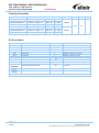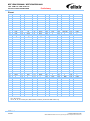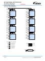
1
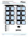
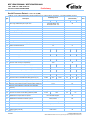
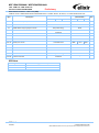
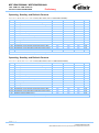
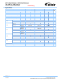
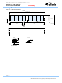
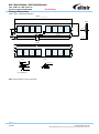
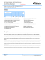
M2F1G64CB88A4N / M2F2G64CB8HA4N 1GB: 128M x 64 / 2GB: 256M x 64 Preliminary Unbuffered DDR3 SDRAM DIMM 240pin Unbuffered DDR3 SDRAM MODULE Based on 128Mx8 DDR3 SDRAM A Die Features • Performance: Speed Sort DIMM Latency fCK Clock Frequency PC3-8500 PC3-10660 PC3-12800 -BE -CG -DG 7 9 9 533 667 800 Unit MHz tCK Clock Cycle 1.875 1.5 1.25 ns fDQ DQ Burst Frequency 1066 1333 1600 Mbps • JEDEC Standard 240-pin Dual In-Line Memory Module • 128Mx64 and 256Mx64 DDR3 Unbuffered DIMM based on 64Mx8 DDR3 Elixir SDRAM • Intended for 533MHz, 667MHz and 800MHz applications • Inputs and outputs are SSTL15 compatible • VDD = VDDQ = 1.5Volt ± 0.075Volt • SDRAMs have 8 internal banks for concurrent operation • Differential clock inputs • Data is read or written on both clock edges • 8 bit pre-fetch • Two different termination values (Rtt_Nom & Rtt_WR) • Extended operating temperature rage • Auto Self-Refresh option • Automatic and controlled precharge commands • Programmable Operation: - DIMM Latency: 5,6,7,8,9,10 - Burst Type: Sequential & Interleave - Burst Length: BC4, BL8 - Operation: Burst Read and Write • 14/10/1 Addressing (row/column/rank) – 1GB • 14/10/2 Addressing (row/column/rank) – 2GB • Serial Presence Detect • Gold contacts • SDRAMs in 78 FBGA Package • RoHS and Halogen-Free compliance Description M2F1G64CB88A4N and M2F2G64CB8HA4N are 240-Pin Double Data Rate 3 (DDR3) Synchronous DRAM Unbuffered Dual In-Line Memory Module (UDIMM), organized as one-rank 128Mx64 and two ranks 256Mx64 high-speed memory array. M2F1G64CB88A4N uses eight 128Mx8 DDR3 SDRAMs. M2F2G64CB8HA4N uses sixteen 128Mx8 DDR3 SDRAMs. These DIMMs are manufactured using raw cards developed for broad industry use as reference designs. The use of these common design files minimizes electrical variation between suppliers. All Elixir DDR3 SDRAM DIMMs provide a high-performance, flexible 8-byte interface in a 5.25” long space-saving footprint. The DIMM is intended for use in applications operating up to 533 MHz ( 667MHz or 800MHz) clock speeds and achieves high-speed data transfer rates of up to 1066Mbps (1333 Mbps or 1600 Mbps). Prior to any access operation, the device latency and burst / length / operation type must be programmed into the DIMM by address inputs A0-A13 and I/O inputs BA0, BA1, and BA2 are using for the mode register set cycle. The DIMM uses serial presence-detect implemented via a serial 2,048-bit EEPROM using a standard IIC protocol. The first 128 bytes of serial PD data are programmed and locked during module assembly. The remaining 128 bytes are available for use by the customer. REV 0.1 06/2008 1 © NANYA TECHNOLOGY CORP. NANYA TECHNOLOGY CORP. reserves the right to change Products and Specifications without notice. M2F1G64CB88A4N / M2F2G64CB8HA4N 1GB: 128M x 64 / 2GB: 256M x 64 Preliminary Unbuffered DDR3 SDRAM DIMM Ordering Information Part Number Speed Organization M2F1G64CB88A4N-BE 533MHz (1.875ns@ CL = 7) DDR3-1066 PC3-8500 M2F1G64CB88A4N-CG 667MHz (1.5ns@ CL = 9) DDR3-1333 PC3-10660 M2F1G64CB88A4N-DG 800 MHz(1.25ns@ CL = 9) DDR3-1600 PC3-12800 M2F2G64CB8HA4N-BE 533MHz (1.875ns@ CL = 7) DDR3-1066 PC3-8500 M2F2G64CB8HA4N-CG 667MHz (1.5ns@ CL = 9) DDR3-1333 PC3-10660 M2F2G64CB8HA4N-DG 800 MHz(1.25ns@ CL = 9) DDR3-1600 PC3-12800 Leads Power Gold 1.5V Note 128Mx64 256Mx64 Pin Description Pin Name Description Pin Name A0-A13 Address Inputs SCL Serial Presence Detect Clock Input Description Serial Presence Detect Data input/output BA0–BA2 SDRAM Bank select SDA Row Address Strobe SA0-SA2 Column Address Strobe VDD SDRAM core power supply Write Enable VDDQ SDRAM I/O Driver power supply Serial Presence Detect Address Inputs , Chip Selects VREFDQ SDRAM I/O reference supply CKE0-CKE1 Clock Enable VREFCA SDRAM command/address reference supply ODT0-ODT1 On die termination control lines DQ0-DQ63 DQS0-DQS7 - VSS Data input/output VDDSPD Ground Serial EEPROM positive power supply SDRAM differential data strobes NC No Connect DM0-DM7 Input Data Mask/High Data Strobes VTT SDRAM I/O termination supply CK0-CK1, - Differential Clock Inputs Note: Set DRAMs to Know State CK1, , OTD1 and CKE1 are used for 2GB module only. REV 0.1 06/2008 2 © NANYA TECHNOLOGY CORP. NANYA TECHNOLOGY CORP. reserves the right to change Products and Specifications without notice. M2F1G64CB88A4N / M2F2G64CB8HA4N 1GB: 128M x 64 / 2GB: 256M x 64 Preliminary Unbuffered DDR3 SDRAM DIMM Pinout Pin Front Pin Front Pin Front Pin 1 VREFDQ 42 NC 2 VSS 43 NC 3 DQ0 44 VSS 4 DQ1 45 NC 5 VSS 46 NC 6 47 VSS 7 DQS0 48 NC 8 VSS Back Pin 82 DQ33 83 VSS 162 NC 202 VSS 163 VSS 203 DM4 84 85 DQ5 164 NC 204 NC VSS 165 NC 205 VSS 86 87 125 DM0 166 VSS 206 DQ38 126 NC 167 NC 207 DQ39 88 DQ35 89 VSS 127 VSS 168 208 VSS 128 DQ6 209 DQ44 9 DQ2 49 NC 90 DQ40 129 DQ7 169 CKE1/NC 210 DQ45 10 DQ3 11 VSS 50 CKE0 51 VDD 91 DQ41 130 VSS 170 VDD 211 VSS 92 VSS 131 DQ12 171 NC 212 DM5 12 13 DQ8 52 BA2 DQ9 53 NC 93 132 DQ13 172 NC 213 NC 94 DQS5 133 VSS 173 VDD 214 VSS 14 VSS 54 VDD 95 VSS 134 DM1 174 A12 / 215 DQ46 15 16 DQS1 55 A11 96 DQ42 135 NC 175 A9 216 DQ47 56 A7 97 DQ43 136 VSS 176 VDD 217 VSS 17 18 VSS 57 VDD 98 VSS 137 DQ14 177 A8 218 DQ52 DQ10 58 A5 99 DQ48 138 DQ15 178 A6 219 DQ53 19 DQ11 20 VSS 59 A4 100 DQ49 139 VSS 179 VDD 220 VSS 60 VDD 101 VSS 140 DQ20 180 A3 221 DM6 21 DQ16 61 A2 102 141 DQ21 181 A1 222 NC 22 DQ17 62 VDD 103 DQS6 142 VSS 182 VDD 223 VSS 23 VSS 63 CK1/NC 104 VSS 143 DM2 183 VDD 224 DQ54 24 64 /NC 105 DQ50 144 NC 184 CK0 225 DQ55 25 DQS2 65 VDD 106 DQ51 145 VSS 185 226 VSS 26 VSS 66 VDD 107 VSS 146 DQ22 186 VDD 227 DQ60 27 DQ18 67 VREFCA 108 DQ56 147 DQ23 187 NC 228 DQ61 28 DQ19 68 NC 109 DQ57 148 VSS 188 A0 229 VSS 29 VSS 69 VDD 110 VSS 149 DQ28 189 VDD 230 DM7 30 DQ24 70 A10/AP 111 150 DQ29 190 BA1 231 NC 31 DQ25 71 BA0 112 DQS7 151 VSS 191 VDD 232 VSS 32 VSS 72 VDD 113 VSS 152 DM3 192 233 DQ62 33 73 114 DQ58 153 NC 193 234 DQ63 34 DQS3 74 115 DQ59 154 VSS 194 VDD 235 VSS 35 VSS 75 VDD 116 VSS 155 DQ30 195 ODT0 236 VDDSPD 36 DQ26 76 /NC 117 SA0 156 DQ31 196 A13 237 SA1 37 DQ27 77 ODT1/NC 118 SCL 157 VSS 197 VDD 238 SDA 38 VSS 78 VDD 119 SA2 158 NC 198 NC 239 VSS 39 NC 79 NC 120 VTT 159 NC 199 VSS 240 VTT 40 NC 80 VSS 160 VSS 200 DQ36 41 VSS 81 DQ32 161 NC 201 DQ37 KEY Back Pin 121 VSS 122 DQ4 123 DQS4 124 VSS DQ34 KEY Back Note: 1. NC = No Connect. 2. Pin 63, 64, 76, 77 and 169 (CK1, , OTD1 and CKE1) are used for 2GB module only. REV 0.1 06/2008 3 © NANYA TECHNOLOGY CORP. NANYA TECHNOLOGY CORP. reserves the right to change Products and Specifications without notice. M2F1G64CB88A4N / M2F2G64CB8HA4N 1GB: 128M x 64 / 2GB: 256M x 64 Preliminary Unbuffered DDR3 SDRAM DIMM Input/Output Functional Description Symbol Type Polarity Function CK0-CK1 - SSTL CKE0-CKE1 SSTL Active High Activates the SDRAM CK signal when high and deactivates the CK signal when low. By deactivating the clocks, CKE low initiates the Power Down mode, or the Self Refresh mode. - SSTL Active Low Enables the associated SDRAM command decoder when low and disables the command decoder when high. When the command decoder is disabled, new commands are ignored but previous operations continue. This signal provides for external rank selection on systems with multiple ranks. , , SSTL Active Low , , (along with ) define the command being entered. VREFDQ Supply Reference voltage for SSTL15 I/O inputs VREFCA Supply Reference voltage for SSTL15 command/address inputs VDDQ Supply CK and are differential clock inputs. All the DDR3 SDRAM address/control inputs Differential are sampled on the crossing of positive edge of CK and negative edge of . Output crossing (read) data is reference to the crossing of CK and . Power supply for the DDR3 SDRAM output buffers to provide improved noise immunity. When high, termination resistance is enabled for all DQ, DQS, , and DM pins, assuming this function is enabled in the Mode Register 1 (MR1). ODT0-ODT1 SSTL Active High BA0 – BA2 SSTL - Selects which SDRAM bank is to be active. During a Bank Activate command cycle, Address input defines the row address (RA0-RA13). During a Read or Write command cycle, Address input defines the column address. In addition to the column address, AP is used to invoke autoprecharge operation at the end of the burst read or write cycle. If AP is low, autoprecharge is disabled. During a Precharge command cycle, AP is used in conjunction with B0 and B1 to control which banks(s) to precharge. If AP is high, all banks will be precharged regardless of the state of BA0, BA1, or BA2. If AP is low, BA0, BA1, and BA2 are used to define which bank to precahrge. A12 () is sampled during READ and WRITE commands to determine if burst chop (on-the –fly) will be performed (High, no burst chop; Low, burst chopped). A0 – A13 SSTL - DQ0 – DQ63 SSTL Active High VDD, VSS Supply DQS0 – DQS7 – SSTL DM0 – DM7 Input Data and Check Bit Input/Output pins. Power and ground for the DDR3 SDRAM input buffers and core logic. Differential Data strobe for input and output data. crossing Active High DM is an input mask signal for write data. Input data is masked when DM is sampled High coincident with that input data during a write access. DM is sampled on both edges of DQS. Although DM pins are input only, the DM loading matches the DQ and DQS loadings. SA0 – SA2 - These signals are tied at the system planar to either Vss or V DDSPD to configure the serial SPD EEPROM address range. SDA - This bi-directional pin is used to transfer data into or out of the SPD EEPROM. A external resistor must be connected from the SDA bus line to VDD to act as a pull-up on the system board. SCL - This signal is used to clock data into and out of the SPD EEPROM. A resistor may be connected from the SCL bus time to V DD to act as a pull-up. VDDSPD REV 0.1 06/2008 Supply Power Supply for SPD EEPROM. This supply is separate from the VDD/VDDQ power plane. EEPROM supply is operable from 3.0V to 3.6V. 4 © NANYA TECHNOLOGY CORP. NANYA TECHNOLOGY CORP. reserves the right to change Products and Specifications without notice. M2F1G64CB88A4N / M2F2G64CB8HA4N 1GB: 128M x 64 / 2GB: 256M x 64 Unbuffered DDR3 SDRAM DIMM Preliminary Functional Block Diagram (1GB, 1 Rank, 128Mx8 DDR3 SDRAMs) DQS0 DM0 DQ0 DQ1 DQ2 DQ3 DQ4 DQ5 DQ6 DQ7 DQS4 DM4 DM I/O 0 I/O 1 I/O 2 I/O 3 D0 I/O 4 I/O 5 I/O 6 I/O 7 DQS DQ32 DQ33 DQ34 DQ35 DQ36 DQ37 DQ38 DQ39 DQS1 DM1 DQ8 DQ9 DQ10 DQ11 DQ12 DQ13 DQ14 DQ15 DM I/O 0 I/O 1 I/O 2 I/O 3 D1 I/O 4 I/O 5 I/O 6 I/O 7 DQS DQ40 DQ41 DQ42 DQ43 DQ44 DQ45 DQ46 DQ47 BA0-BA2 A0-A13 DM I/O 0 I/O 1 I/O 2 I/O 3 D2 I/O 4 I/O 5 I/O 6 I/O 7 DQS DQ48 DQ49 DQ50 DQ51 DQ52 DQ53 DQ54 DQ55 DM I/O 0 I/O 1 I/O 2 I/O 3 D3 I/O 4 I/O 5 I/O 6 I/O 7 DQS DQS DQ56 DQ57 DQ58 DQ59 DQ60 DQ61 DQ62 DQ63 DM I/O 0 I/O 1 I/O 2 I/O 3 D7 I/O 4 I/O 5 I/O 6 I/O 7 DQS A0-A13 : SDRAMs D0-D7 : SDRAMs D0-D7 ODT0 DM I/O 0 I/O 1 I/O 2 I/O 3 D6 I/O 4 I/O 5 I/O 6 I/O 7 BA0-BA2 : SDRAMs D0-D7 : SDRAMs D0-D7 CKE0 DQS DQS7 DM7 DM I/O 0 I/O 1 I/O 2 I/O 3 D5 I/O 4 I/O 5 I/O 6 I/O 7 DQS6 DM6 DQS3 DM3 DQ24 DQ25 DQ26 DQ27 DQ28 DQ29 DQ30 DQ31 DQS DQS5 DM5 DQS2 DM2 DQ16 DQ17 DQ18 DQ19 DQ20 DQ21 DQ22 DQ23 DM I/O 0 I/O 1 I/O 2 I/O 3 D4 I/O 4 I/O 5 I/O 6 I/O 7 VDDSPD VDD/VDDQ VREFDQ VSS VREFCA : SDRAMs D0-D7 SPD D0-D7 D0-D7 D0-D7 D0-D7 CKE : SDRAMs D0-D7 ODT : SDRAMs D0-D7 CK0 CK : SDRAMs D0-D7 : SDRAMs D0-D7 Serial PD SCL WPA0 SA0 REV 0.1 06/2008 A1 A2 SA1 SA2 SDA 5 © NANYA TECHNOLOGY CORP. NANYA TECHNOLOGY CORP. reserves the right to change Products and Specifications without notice. M2F1G64CB88A4N / M2F2G64CB8HA4N 1GB: 128M x 64 / 2GB: 256M x 64 Unbuffered DDR3 SDRAM DIMM Preliminary Functional Block Diagram (2GB, 2 Rank, 128Mx8 DDR3 SDRAMs) DQS0 DM0 DQS4 DM4 DM I/O 0 I/O 1 I/O 2 I/O 3 D0 I/O 4 I/O 5 I/O 6 I/O 7 DQ0 DQ1 DQ2 DQ3 DQ4 DQ5 DQ6 DQ7 DQS DM I/O 0 I/O 1 I/O 2 I/O 3 D8 I/O 4 I/O 5 I/O 6 I/O 7 DQS DQ32 DQ33 DQ34 DQ35 DQ36 DQ37 DQ38 DQ39 DQS1 DM1 DQS DM I/O 0 I/O 1 I/O 2 I/O 3 D12 I/O 4 I/O 5 I/O 6 I/O 7 DQS DM I/O 0 I/O 1 I/O 2 I/O 3 D5 I/O 4 I/O 5 I/O 6 I/O 7 DQS DM I/O 0 I/O 1 I/O 2 I/O 3 D13 I/O 4 I/O 5 I/O 6 I/O 7 DQS DM I/O 0 I/O 1 I/O 2 I/O 3 D6 I/O 4 I/O 5 I/O 6 I/O 7 DQS DM I/O 0 I/O 1 I/O 2 I/O 3 D14 I/O 4 I/O 5 I/O 6 I/O 7 DQS DM I/O 0 I/O 1 I/O 2 I/O 3 D7 I/O 4 I/O 5 I/O 6 I/O 7 DQS DM I/O 0 I/O 1 I/O 2 I/O 3 D15 I/O 4 I/O 5 I/O 6 I/O 7 DQS DQS5 DM5 DM I/O 0 I/O 1 I/O 2 I/O 3 D1 I/O 4 I/O 5 I/O 6 I/O 7 DQ8 DQ9 DQ10 DQ11 DQ12 DQ13 DQ14 DQ15 DQS DM I/O 0 I/O 1 I/O 2 I/O 3 D9 I/O 4 I/O 5 I/O 6 I/O 7 DQS DQ40 DQ41 DQ42 DQ43 DQ44 DQ45 DQ46 DQ47 DQS2 DM2 DQS6 DM6 DM I/O 0 I/O 1 I/O 2 I/O 3 D2 I/O 4 I/O 5 I/O 6 I/O 7 DQ16 DQ17 DQ18 DQ19 DQ20 DQ21 DQ22 DQ23 DQS DM I/O 0 I/O 1 I/O 2 I/O 3 D10 I/O 4 I/O 5 I/O 6 I/O 7 DQS DQ48 DQ49 DQ50 DQ51 DQ52 DQ53 DQ54 DQ55 DQS3 DM3 DQS7 DM7 DM I/O 0 I/O 1 I/O 2 I/O 3 D3 I/O 4 I/O 5 I/O 6 I/O 7 DQ24 DQ25 DQ26 DQ27 DQ28 DQ29 DQ30 DQ31 BA0-BA2 A0-A13 DQS DQS DQ56 DQ57 DQ58 DQ59 DQ60 DQ61 DQ62 DQ63 A0-A13: SDRAMs D0-D15 : SDRAMs D0-D15 : SDRAMs D0-D15 : SDRAMs D0-D15 CKE0 CKE : SDRAMs D0-D7 CKE1 CKE : SDRAMs D8-D15 ODT0 ODT : SDRAMs D0-D7 VDDSPD VDD/VDDQ VREFDQ VSS VREFCA SPD D0-D15 D0-D15 D0-D15 D0-D15 ODT : SDRAMs D8-D15 CK0 CK: SDRAMs D0-D7 CK1 CK: SDRAMs D8-D15 : SDRAMs D0-D7 : SDRAMs D8-D15 REV 0.1 DM I/O 0 I/O 1 I/O 2 I/O 3 D11 I/O 4 I/O 5 I/O 6 I/O 7 BA0-BA2 : SDRAMs D0-D15 ODT1 06/2008 DM I/O 0 I/O 1 I/O 2 I/O 3 D4 I/O 4 I/O 5 I/O 6 I/O 7 Serial PD SCL WP A0 A1 A2 SA0 SA1 SA2 SDA 6 © NANYA TECHNOLOGY CORP. NANYA TECHNOLOGY CORP. reserves the right to change Products and Specifications without notice. M2F1G64CB88A4N / M2F2G64CB8HA4N 1GB: 128M x 64 / 2GB: 256M x 64 Unbuffered DDR3 SDRAM DIMM Preliminary Serial Presence Detect -- Part 1 of 2 (1GB) 128Mx64 1 Rank UNBUFFERED DDR3 SDRAM DIMM based on 128Mx8, 8Banks, 8K Refresh, 1.5V DDR3 SDRAMs with SPD Byte -BE 0 CRC range, EEPROM bytes, bytes used 1 SPD revision 2 DRAM device type 3 Module type (form factor) 4 SDRAM Device density and banks 5 SDRAM device row and column count 6 Reserved 7 Module ranks and device DQ count 8 ECC tag and module memory Bus width 9 Fine timebase dividend/divisor (in ps) 10 Serial PD Data Entry (Hexadecimal) SPD Entry Value Description -CG -DG -BE CRC Covers Bytes: 0~116, Total SPD Bytes: 256, SPD Bytes Used: 176, -CG 92 Revision 0.8 08 DDR3 SDRAM 0B UDIMM 02 8 banks, 1Gb 02 14 rows, 10 columns 11 Undefined 00 1 ranks, 8 bits 01 Non ECC, 64bits 03 2.5ps 52 Medium timebase dividend 1ns 01 11 Medium timebase divisor 8ns 08 12 Minimum SDRAM cycle time (tCKmin) (ns) 13 Reserved 14 CAS latencies supported 15 CAS latencies supported 16 Minimum CAS latency time (tAAmin) (ns) 17 Minimum write recovery time (tWRmin) 18 Minimum -to- delay (tRCDmin) (ns) 19 Minimum Row Active to Row Active delay (tRRDmin) (ns) 20 Minimum row Precharge delay (tRPmin) (ns) 21 Upper nibble for tRAS and tRC 22 Minimum Active-to-Precharge delay (tRASmin) (ns) 23 Minimum Active-to-Active/Refresh delay (tRCmin) (ns) 24 Minimum refresh recovery delay (tRFCmin) LSB (Combo bytes 24,25) 25 Minimum refresh recovery delay (tRFCmin) MSB 110ns 03 26 Minimum internal Write-to-Read command delay (tWTRmin) 7.5ns 3C 27 Minimum internal Read-to-Precharge command delay (tRTPmin) 7.5ns 3C 28 Minimum four active window delay (tFAWmin) LSB 29 Minimum four active window delay (tFAWmin) MSB 30 SDRAM device output drivers suported 31 SDRAM device thermal and refresh options 32 Module thermal sensor 33 SDRAM device type 1.875 6,7,8 06/2008 0F 6,8,9 13.125 5,6,7,8,9,10 1C 13.5 11.25 34 7E 69 6C 5A 78 13.5 11.25 7.5 6 13.125 0A 00 15ns 13.125 0C 00 Undefined 13.5 69 6C 3C 11.25 69 1,1 5A 30 6C 5A 11 37.5 36 35 2C 20 18 50.625 49.5 46.25 95 8C 72 (Combo byte 28, 29) 37.5ns 30ns 70 01 00 2C F0 RZQ / 6,RZQ / 7, DLL-Off Mode Support, 83 Extended Temperature Range, ASR, ODTS, PASR, 8D Non Thermal Sensor Support -- height ≦ 15mm 0F thickness ≤ 1 mm 11 Raw Card A 00 Module height (nominal) REV 0.1 1.25 Undefined 34-59 Reserved 60 1.5 -DG 7 © NANYA TECHNOLOGY CORP. NANYA TECHNOLOGY CORP. reserves the right to change Products and Specifications without notice. Note M2F1G64CB88A4N / M2F2G64CB8HA4N 1GB: 128M x 64 / 2GB: 256M x 64 Unbuffered DDR3 SDRAM DIMM Preliminary Serial Presence Detect -- Part 2 of 2 (1GB) 128Mx64 1 Rank UNBUFFERED DDR3 SDRAM DIMM based on 128Mx8, 8Banks, 8K Refresh, 1.5V DDR3 SDRAMs with SPD Byte Serial PD Data Entry (Hexadecimal) SPD Entry Value Description -BE -CG -DG -BE -CG 61 Module thickness (Max) Standard 00 62 Raw Card ID reference Undefined -- 63 DRAM address mapping edge connector Nanya Technology 830B 64-116 Reserved Undefined 00 117-118 Module manufacture ID Undefined 00 119-125 Module information Undefined 00 126-127 CRC Undefined 00000000 128-145 Module part number Calculated Value 146 Module die revision ASCII values -- 147 Module PCB revision Undefined 00 148-149 DRAM device manufacturer ID Undefined 00 150-175 Manufacturer reserved Nanya Technology 830B 176-255 Customer reserved Undefined -- 227A F05C -DG E202 SPD Note SPD Entry Value Serial PD Data Entry (Hexadecimal) M2F1G64CB88A4N-BE 4D3246314736344342383841344E2D424520 M2F1G64CB88A4N-CG 4D3246314736344342383841344E2D434720 M2F1G64CB88A4N-DG 4D3246314736344342383841344E2D444720 REV 0.1 06/2008 8 © NANYA TECHNOLOGY CORP. NANYA TECHNOLOGY CORP. reserves the right to change Products and Specifications without notice. Note M2F1G64CB88A4N / M2F2G64CB8HA4N 1GB: 128M x 64 / 2GB: 256M x 64 Unbuffered DDR3 SDRAM DIMM Preliminary Serial Presence Detect -- Part 1 of 2 (2GB) 256Mx64 2 Ranks UNBUFFERED DDR3 SDRAM DIMM based on 128Mx8, 8Banks, 8K Refresh, 1.5V DDR3 SDRAMs with SPD Byte -BE 0 CRC range, EEPROM bytes, bytes used 1 SPD revision 2 DRAM device type 3 Module type (form factor) 4 SDRAM Device density and banks 5 SDRAM device row and column count 6 Reserved 7 Module ranks and device DQ count 8 ECC tag and module memory Bus width 9 Fine timebase dividend/divisor (in ps) 10 Serial PD Data Entry (Hexadecimal) SPD Entry Value Description -CG -DG -BE -CG CRC Covers Bytes: 0~116, Total SPD Bytes: 256, SPD Bytes Used: 176, 92 Revision 0.8 08 DDR3 SDRAM 0B UDIMM 02 8 banks, 1Gb 02 14 rows, 10 columns 11 Undefined 00 2 ranks, 8 bits 09 Non ECC, 64bits 03 2.5ps 52 Medium timebase dividend 1ns 01 11 Medium timebase divisor 8ns 08 12 Minimum SDRAM cycle time (tCKmin) (ns) 13 Reserved 14 CAS latencies supported 15 CAS latencies supported 16 Minimum CAS latency time (tAAmin) (ns) 17 Minimum write recovery time (tWRmin) 18 Minimum -to- delay (tRCDmin) (ns) 19 Minimum Row Active to Row Active delay (tRRDmin) (ns) 20 Minimum row Precharge delay (tRPmin) (ns) 21 Upper nibble for tRAS and tRC 22 Minimum Active-to-Precharge delay (tRASmin) (ns) 23 Minimum Active-to-Active/Refresh delay (tRCmin) (ns) 24 Minimum refresh recovery delay (tRFCmin) LSB (Combo bytes 24,25) 70 25 Minimum refresh recovery delay (tRFCmin) MSB 110ns 03 26 Minimum internal Write-to-Read command delay (tWTRmin) 7.5ns 3C 27 Minimum internal Read-to-Precharge command delay (tRTPmin) 7.5ns 3C 28 Minimum four active window delay (tFAWmin) LSB 29 Minimum four active window delay (tFAWmin) MSB 30 SDRAM device output drivers suported 31 SDRAM device thermal and refresh options 32 Module thermal sensor 33 SDRAM device type 1.875 6,7,8 06/2008 0F 6,8,9 13.125 5,6,7,8,9,10 1C 13.5 11.25 34 7E 69 6C 5A 78 13.5 11.25 7.5 6 13.125 0A 00 15ns 13.125 0C 00 Undefined 13.5 69 6C 3C 11.25 69 1,1 5A 30 6C 5A 11 37.5 36 35 2C 20 18 50.625 49.5 46.25 95 8C 72 (Combo byte 28, 29) 37.5ns 30ns 01 00 2C F0 RZQ / 6,RZQ / 7, DLL-Off Mode Support, 83 Extended Temperature Range, ASR, ODTS, PASR, 8D Non Thermal Sensor Support -- height ≦ 15mm 0F thickness ≤ 1 mm 11 Raw Card B 01 Module height (nominal) REV 0.1 1.25 Undefined 34-59 Reserved 60 1.5 -DG 9 © NANYA TECHNOLOGY CORP. NANYA TECHNOLOGY CORP. reserves the right to change Products and Specifications without notice. Note M2F1G64CB88A4N / M2F2G64CB8HA4N 1GB: 128M x 64 / 2GB: 256M x 64 Unbuffered DDR3 SDRAM DIMM Preliminary Serial Presence Detect -- Part 2 of 2 (2GB) 256Mx64 2 Ranks UNBUFFERED DDR3 SDRAM DIMM based on 128Mx8, 8Banks, 8K Refresh, 1.5V DDR3 SDRAMs with SPD Byte Serial PD Data Entry (Hexadecimal) SPD Entry Value Description -BE -CG -DG -BE -CG 61 Module thickness (Max) Standard 01 62 Raw Card ID reference Undefined -- 63 DRAM address mapping edge connector Nanya Technology 830B 64-116 Reserved Undefined 00 117-118 Module manufacture ID Undefined 00 119-125 Module information Undefined 00 126-127 CRC Undefined 00000000 128-145 Module part number Calculated Value 146 Module die revision ASCII values -- 147 Module PCB revision Undefined 00 148-149 DRAM device manufacturer ID Undefined 00 150-175 Manufacturer reserved Nanya Technology 830B 176-255 Customer reserved Undefined -- ABEF 79C9 -DG 6B97 SPD Note SPD Entry Value Serial PD Data Entry (Hexadecimal) M2F1G64CB88A4N-BE 4D3246324736344342384841344E2D424520 M2F1G64CB88A4N-CG 4D3246324736344342384841344E2D434720 M2F1G64CB88A4N-DG 4D3246324736344342384841344E2D444720 REV 0.1 06/2008 10 © NANYA TECHNOLOGY CORP. NANYA TECHNOLOGY CORP. reserves the right to change Products and Specifications without notice. Note M2F1G64CB88A4N / M2F2G64CB8HA4N 1GB: 128M x 64 / 2GB: 256M x 64 Preliminary Unbuffered DDR3 SDRAM DIMM Absolute Maximum DC Ratings Symbol VIN, VOUT VDD VDDQ Parameter Rating Units Voltage on I/O pins relative to Vss -0.4 to 1.975 V Voltage on VDD supply relative to Vss -0.4 to 1.975 V Voltage on VDDQ supply relative to Vss -0.4 to 1.975 V Note: Stresses greater than those listed under “Absolute Maximum Ratings” may cause permanent damage to the device. This is stress rating only, and functional operation of the device at these or any other conditions above those indicated in the operational sections of this specification is not implied. Exposure to absolute maximum rating conditions for extended periods may affect reliability. DC Electrical Characteristics and Operating Conditions (TCASE = 0 °C ~ 85 °C; VDDQ = 1.5V ± 0.075V; VDD = 1.5V ± 0.075V, See AC Characteristics) Symbol Parameter VDD Supply Voltage VDDQ I/O Supply Voltage VREF I/O Reference Voltage Min Max Units Notes 1.425 1.575 V 1 1.425 1.575 V 1 0.49VDDQ 0.51VDDQ V 1, 2 Note: 1. Inputs are not recognized as valid until VREF stabilizes. 2. VREF is expected to be equal to 0.5 V DDQ of the transmitting device, and to track variations in the DC level of the same. Peak-to-peak noise on VREF may not exceed 2% of the DC value. Environmental Parameters Symbol TOPR HOPR Parameter Rating Units Note Module Operating Temperature Range (ambient) 0 to 55 °C 3 Operating Humidity (relative) 10 to 90 % 1 -50 to 100 °C 1 5 to 95 % 1 105 to 69 K Pascal 1,2 TSTG Storage Temperature (Plastic) HSTG Storage Humidity (without condensation) PBAR Barometric Pressure (operating & storage) Note: 1. 2. 3. Stresses greater than those listed may cause permanent damage to the device. This is a tress rating only, and device functional operation at or above the conditions indicated is not implied. Exposure to absolute maximum rating conditions for extended periods may affect reliability. Up to 9850 ft. The component maximum case temperature shall not exceed the value specified in the component spec. Single Ended AC and DC Input Levels DDR3-1066, DDR3-1333, DDR3-1600 Symbol Parameter VIH (DC) DC input logic high Vref + 0.100 VIL (DC) DC input logic low VSS VIH (AC) Units Note VDD V 1 Vref – 0.100 V 1 Min. V 1 AC input logic low - Vref – 0.175 V 1 VrefDQ(DC) Reference Voltage for DQ, DM inputs 0.49 * VDD 0.51 * VDD V 2,3 VrefCA(DC) Reference Voltage for ADD, CMD inputs 0.49 * VDD 0.51 * VDD V 2,3 VIL (AC) AC input logic high Max. Vref + 0.175 Note: 1. For DQ and DM, Vref = VrefDQ. For input only pins except , Vref = VrefCA. 2. The AC peak noise on Vref may not allow Vref to deviate from Vref(DC) by more than +/- 1% VDD. 3. For reference: approx. VDD/2 +/- 15mV. REV 0.1 06/2008 11 © NANYA TECHNOLOGY CORP. NANYA TECHNOLOGY CORP. reserves the right to change Products and Specifications without notice. M2F1G64CB88A4N / M2F2G64CB8HA4N 1GB: 128M x 64 / 2GB: 256M x 64 Unbuffered DDR3 SDRAM DIMM Preliminary Operating, Standby, and Refresh Currents TCASE = 0 °C ~ 85 °C; VDDQ = VDD = 1.5V ± 0.075V (1GB, 1 Rank, base on 128Mx8 DDR3 SDRAMs) Symbol DDR3-1066 DDR3-1333 DDR3-1600 Unit I DD0 Operating Current: one bank activate/Precharge Parameter/Condition TBD TBD TBD mA I DD1 Operating Current: one bank activate/Read/Precharge TBD TBD TBD mA I DD2P(0) Precharge Power-Down Current Fast Exit-MR0 bit A12=0 TBD TBD TBD mA I DD2P(1) Precharge Power Down Current Slow Exit-MR0 bit A12=1 TBD TBD TBD mA I DD2N Precharge Standby Current TBD TBD TBD mA I DD2Q Precharge Quiet Standby current TBD TBD TBD mA I DD3P Active Power-Down Current Always Fast Exit TBD TBD TBD mA I DD3N Active Standby Current TBD TBD TBD mA I DD4W Operating Current: Burst Write TBD TBD TBD mA I DD4R Operating Current: Burst Read TBD TBD TBD mA I DD5B Burst Refresh Current TBD TBD TBD mA I DD6 Self-Refresh Current Normal Temperature Range (0-85C) TBD TBD TBD mA TBD TBD TBD mA TBD TBD TBD mA I DD6ET Self-Refresh Current Extended Temperature Range (0-95C) I DD7 All Bank Interleave Read Current Note: Module IDD was calculated from component IDD. It may differ from the actual measurement. Operating, Standby, and Refresh Currents TCASE = 0 °C ~ 85 °C; VDDQ = VDD = 1.5V ± 0.075V (2GB, 2 Ranks, base on 128Mx8 DDR3 SDRAMs) Symbol Parameter/Condition DDR3-1066 DDR3-1333 DDR3-1600 Unit I DD0 Operating Current: one bank activate/Precharge TBD TBD TBD mA I DD1 Operating Current: one bank activate/Read/Precharge TBD TBD TBD mA I DD2P(0) Precharge Power-Down Current Fast Exit-MR0 bit A12=0 TBD TBD TBD mA I DD2P(1) Precharge Power Down Current Slow Exit-MR0 bit A12=1 TBD TBD TBD mA I DD2N Precharge Standby Current TBD TBD TBD mA I DD2Q Precharge Quiet Standby current TBD TBD TBD mA I DD3P Active Power-Down Current Always Fast Exit TBD TBD TBD mA I DD3N Active Standby Current TBD TBD TBD mA I DD4W Operating Current: Burst Write TBD TBD TBD mA I DD4R Operating Current: Burst Read TBD TBD TBD mA I DD5B Burst Refresh Current TBD TBD TBD mA I DD6 Self-Refresh Current Normal Temperature Range (0-85C) TBD TBD TBD mA TBD TBD TBD mA TBD TBD TBD mA I DD6ET Self-Refresh Current Extended Temperature Range (0-95C) I DD7 All Bank Interleave Read Current Note: Module IDD was calculated from component IDD. It may differ from the actual measurement. REV 0.1 06/2008 12 © NANYA TECHNOLOGY CORP. NANYA TECHNOLOGY CORP. reserves the right to change Products and Specifications without notice. M2F1G64CB88A4N / M2F2G64CB8HA4N 1GB: 128M x 64 / 2GB: 256M x 64 Preliminary Unbuffered DDR3 SDRAM DIMM Speed Bins Speed Bin DDR3-1066 (-BE) 7-7-7 CL - nRCD - nRP Parameter Internal read command to first data DDR3-1333 (-CG) 9-9-9 DDR3-1600(-DG) 9-9-9 Unit Symbol Min Max Min Max Min Max tAA 13.125 20 13.5 20 11.25 20 ns -- 11.25 -- ns tRCD 13.125 -- 13.5 PRE command period tRP 13.125 -- 13.5 -- 11.25 -- ns ACT to ACT or REF command period tRC 50.625 -- 49.5 -- 46.25 -- ns tRAS 37.5 9*tREFI 36 9*tREFI 35 9*tREFI 2.5 3.3 ns ns ACT to internal read or write delay time ACT to PRE command period CL = 5 CL = 6 CL = 7 CL = 8 CL = 9 CWL=5 tCK(AVG) Reserved Reserved CWL=6, 7, 8 tCK(AVG) Reserved Reserved CWL=5 tCK(AVG) CWL=6 tCK(AVG) Reserved Reserved CWL=7, 8 tCK(AVG) Reserved Reserved CWL=5 tCK(AVG) Reserved Reserved CWL=6 tCK(AVG) CWL=7 tCK(AVG) Reserved Reserved Reserved ns CWL=8 tCK(AVG) Reserved Reserved Reserved ns CWL=5 tCK(AVG) Reserved ns CWL=6 tCK(AVG) CWL=7 tCK(AVG) Reserved Reserved CWL=8 tCK(AVG) Reserved Reserved Reserved ns CWL=5, 6 tCK(AVG) Reserved Reserved Reserved ns CWL=7 tCK(AVG) Reserved CWL=8 tCK(AVG) Reserved Reserved 6,7,8 6,8,9 5,6,7 Supported CL settings Supported CWL Settings REV 0.1 06/2008 2.5 3.3 1.875 <2.5 Reserved 1.875 <2.5 5,6 2.5 Reserved 3.3 Reserved Reserved 1.875 <2.5 1.5 <1.875 ns 2.5 3.3 ns 1.875 <2.5 ns Reserved ns Reserved ns 1.875 <2.5 ns 1.875 <2.5 ns 1.5 <1.875 ns 1.5 <1.875 ns 1.25 <1.5 ns 5,6,7,8,9,10 5,6,7,8 nCK nCK 13 © NANYA TECHNOLOGY CORP. NANYA TECHNOLOGY CORP. reserves the right to change Products and Specifications without notice. M2F1G64CB88A4N / M2F2G64CB8HA4N 1GB: 128M x 64 / 2GB: 256M x 64 Preliminary Unbuffered DDR3 SDRAM DIMM AC Timing Specifications for DDR3 SDRAM Devices Used on Module DDR3-1066 Parameter DDR3-1333 Symbol Min Max Min tCK(DLL_O FF) 8 - 8 Average high pulse width tCH(avg) 0.47 0.53 0.47 Average low pulse width tCL(avg) 0.47 0.53 Absolute Clock Period tCK(abs) tCK(avg)min +tJIT(per)min tCK(avg)max +tJIT(per)max Absolute clock high pulse width tCH(abs) 0.43 - Absolute clock low pulse width tCL(abs) 0.43 - Clock Period Jitter tJIT(per) -90 tJIT(per,lck) -80 Max Units Clock Timing Minimum Clock Cycle time (DLL off mode) Clock Period Jitter during DLL locking period Cycle to Cycle Period Jitter Cycle to Cycle Period Jitter during DLL locking period Duty Cycle Jitter ns 0.53 tCK(avg) 0.47 0.53 tCK(avg) tCK(avg)min +tJIT(per)min tCK(avg)max +tJIT(per)max ps 0.43 - ps 0.43 - ps 90 -80 80 ps 80 -70 70 ps tJIT(cc) 180 160 ps tJIT(cc,lck) 160 140 ps tJIT(duty) - - - - ps Cumulative error across 2 cycles tERR(2per) -132 132 -118 118 ps Cumulative error across 3 cycles tERR(3per) -157 157 -140 140 ps Cumulative error across 4 cycles tERR(4per) -175 175 -155 155 ps Cumulative error across 5 cycles tERR(5per) -188 188 -168 168 ps Cumulative error across 6 cycles tERR(6per) -200 200 -177 177 ps Cumulative error across 7 cycles tERR(7per) -209 209 -186 186 ps Cumulative error across 8 cycles tERR(8per) -217 217 -193 193 ps Cumulative error across 9 cycles tERR(9per) -224 224 -200 200 ps Cumulative error across 10 cycles tERR(10per) -231 231 -205 205 ps Cumulative error across n=11~50 cycles tERR(npr)min tERR(npr)max tERR(npr)min tERR(npr)max tERR(nper) =(1+0.68In(n))*tJIT =(1+0.68In(n))*tJIT =(1+0.68In(n))*tJIT =(1+0.68In(n))*tJIT (per)min (per)max (per)min (per)max ps Data Timing DQS, to DQ skew, per group, per access tDQSQ - 150 tQH 0.38 - 0.38 DQ low-impedance time from CK, tLZ(DQ) -600 300 -500 DQ high-impedance time from CK, tHZ(DQ) - 300 DQ output hold time from DQS, Data setup time to DQS, DQS reference to Vih(ac) / tDS(base) Vil(ac) levels Data hold time to DQS, DQS reference to Vih(ac) / Vil(ac) tDH(base) levels 125 ps tCK(avg) 250 ps 250 ps 25 TBD ps 100 TBD ps Data Strobe Timing DQS, differential READ Preamble tRPRE DQS, differential READ Postamble DQS, differential output high time DQS, differential output low time 0.9 - 0.9 - tCK(avg) tRPST 0.3 tQSH 0.38 - 0.3 - tCK(avg) - 0.40 tCK(avg) tQSL 0.38 - 0.40 tCK(avg) DQS, differential WRITE Preamble DQS, differential WRITE Postamble tWPRE 0.9 - 0.9 tCK(avg) tWPST 0.3 - 0.3 tCK(avg) DQS, rising dege output access time from rising CK, tDQSCK -300 300 -255 255 ps DQS, low-impedance time (Reference from RL-1) tLZ(DQS) -600 300 -500 250 ps tHZ(DQS) - 300 250 ps DQS, high-impedance time (Reference from RL + BL/2) DQS, differential input low pulse width tDQSL 0.4 0.6 0.4 0.6 tCK(avg) DQS, differential input high pulse width tDQSH 0.4 0.6 0.4 0.6 tCK(avg) DQS, rising edge to CK, rising edge tDQSS -0.25 0.25 -0.25 0.25 tCK(avg) DQS, falling edge setup time to CK, rising edge tDSS 0.2 - 0.2 - tCK(avg) DQS, falling edge hold time to CK, rising edge tDSH 0.2 - 0.2 - tCK(avg) REV 0.1 06/2008 14 © NANYA TECHNOLOGY CORP. NANYA TECHNOLOGY CORP. reserves the right to change Products and Specifications without notice. M2F1G64CB88A4N / M2F2G64CB8HA4N 1GB: 128M x 64 / 2GB: 256M x 64 Preliminary Unbuffered DDR3 SDRAM DIMM Parameter Command and Address Timing Symbol DDR3-1066 Min Max Min DDR3-1333 Max Units DLL locking time Internal READ Command to PRECHARGE Command delay Delay from start of internal write transaction to internal read command WRITE recovery time tDLLK 512 - 512 - tRTP max(4nCK, 7.5ns) - max(4nCK, 7.5ns) - tWTR max(4nCK, 7.5ns) - max(4nCK, 7.5ns) - tWR 15 - 15 - ns Mode Register Set command cycle time tMRD 4 - 4 - nCK Mode Register Set command update delay tMOD max(12nCK, 15ns) - max(12nCK, 15ns) - to command delay tCCD 4 - 4 - Auto precharge write recovery + precharge time Multi-Purpose Register Recovery Time tDAL(min) WR + roundup (tRP/tCK(avg)) nCK nCK nCK tMPRR 1 - 1 - ACTIVE to ACTIVE command period for 1KB page size tRRD max(4nCK, 7.5ns) - max(4nCK, 6ns) - Four activate window for 1KB page size Command and Address setup time to CK, referenced to Vih(ac) / Vil(ac) levels Command and Address hold time to CK, referenced to Vih(ac) / Vil(ac) levels tFAW 37.5 - 30 - ns tIS(base) 125 - 65 - ps tIH(base) 200 - 140 - ps Power-up and RESET calibration time tZQinit 512 - 512 - nCK Normal operation Full calibration time tZQoper 256 - 256 - nCK tZQCS 64 - 64 - nCK tXPR max(5nCK, tRFC(min) + 10ns) - max(5nCK, tRFC(min) + 10ns) - Calibrating Timing Normal operation Short calibration time Reset Timing Exit Reset from CKE HIGH to a valid command Self Refresh Timings Exit Self Refresh to commands not requiring a locked DLL Exit Self Refresh to commands requiring a locked DLL Minimum CKE low width for Self Refresh entry to exit timing Valid Clock Requirement after Self Refresh Entry (SRE) or Power-Down Entry (PDE) Valid Clock Requirement after Self Refresh Exit (SRX) or Power-Down Exit (PDX) or Reset Exit tXS tXSDLL tCKESR max(5nCK, tRFC(min) + 10ns) tDLLK(min) tCKE(min) + 1nCK - max(5nCK, tRFC(min) + 10ns) tDLLK(min) tCKE(min) + 1nCK - nCK - tCKSRE max(5nCK, 10ns) - max(5nCK, 10ns) - tCKSRX max(5nCK, 10ns) - max(5nCK, 10ns) - tXP max(3nCK, 7.5ns) - max(3nCK, 6ns) - tXPDLL max(10nCK, 24ns) - max(10nCK, 24ns) - Power Down Timings Exit Power Down with DLL on to any valid command; Exit Precharge Power Down with DLL frozen to commands not requiring a locked DLL Exit Precharge Power Down with DLL frozen to commands requiring a locked DLL tCPDED max(3nCK, 5.625ns) 1 - max(3nCK, 5.625ns) 1 tPD tCKE(min) 9*tREFI tCKE(min) 9*tREFI tACTPDEN 1 - 1 - nCK tPRPDEN 1 - 1 - nCK Timing of RD/RDA command to Power Down entry tRDPDEN RL+4+1 Timing of WR command to Power Down entry (BL8OTF, WL+4+(tWR/tCK(a tWRPDEN BL8MRS, BC4OTF) vg)) Timing of WRA command to Power Down entry tWRAPDEN WL+4+WR+1 (BL8OTF, BL8MRS, BC4OTF) WL+2+(tWR/tCK(a Timing of WR command to Power Down entry (BC4MRS) tWRPDEN vg)) Timing of WRA command to Power Down entry tWRAPDEN WL+2+WR+1 (BC4MRS) Timing of REF command to Power down entry tREFPDEN 1 - RL+4+1 WL+4+(tWR/tCK(a vg)) - nCK - nCK - WL+4+WR+1 - nCK - WL+2+(tWR/tCK(a vg)) - nCK - WL+2+WR+1 - nCK - 1 - nCK Timing of MRS command to Power Down entry - tMOD(min) - CKE minimum pulse width Command pass disable delay Power Down Entry to Exit Timing Timing of ACT command to Power Down entry Timing of PRE or PREA command to Power Down entry REV 0.1 06/2008 tCKE tMRSPDEN tMOD(min) - - - nCK 15 © NANYA TECHNOLOGY CORP. NANYA TECHNOLOGY CORP. reserves the right to change Products and Specifications without notice. M2F1G64CB88A4N / M2F2G64CB8HA4N 1GB: 128M x 64 / 2GB: 256M x 64 Preliminary Unbuffered DDR3 SDRAM DIMM DDR3-1066 Parameter DDR3-1333 Symbol Min Max Min Max Units ODT high time without write command or with write command and BC4 ODTH4 4 - 4 - nCK ODT high time with Write command and BL8 ODTH8 6 - 6 - nCK tAONPD 1 9 1 9 ns tAOFPD 1 9 1 9 ns RTT turn-on tAON -300 300 -250 250 ps RTT_Nom and RTT_WR turn-off time from ODTLoff reference tAOF 0.3 0.7 0.3 0.7 tCK(avg) RTT dynamic change skew tADC 0.3 0.7 0.3 0.7 tCK(avg) tWLMRD 40 - 40 - nCK tWLDQSEN 25 - 25 - nCK tWLS 245 - 195 - ps tWLH 245 - 195 - ps Write leveling output delay tWLO 0 9 0 9 ns Write leveling output error tWLOE 0 2 0 2 ns ODT Timings Asynchronous RTT turn-on delay (Power - Down with DLL frozen) Asynchronous RTT turn-off delay (Power – Down with DLL frozen) Write Leveling Timings First DQS/ rising edge after write leveling mode is programmed DQS/DQS delay after write leveling mode is programmed Write leveling setup time from rising CK, crossing to rising DQS, crossing Write leveling setup hold from rising CK, crossing to rising DQS, crossing REV 0.1 06/2008 16 © NANYA TECHNOLOGY CORP. NANYA TECHNOLOGY CORP. reserves the right to change Products and Specifications without notice. M2F1G64CB88A4N / M2F2G64CB8HA4N 1GB: 128M x 64 / 2GB: 256M x 64 Unbuffered DDR3 SDRAM DIMM Preliminary AC Timing Specifications for DDR3 SDRAM Devices Used on Module DDR3-1600 Parameter Symbol Min Max Units tCK(DLL_OFF) 8 - ns Average high pulse width tCH(avg) 0.47 0.53 tCK(avg) Average low pulse width tCL(avg) 0.47 0.53 tCK(avg) Absolute Clock Period tCK(abs) Absolute clock high pulse width tCH(abs) 0.43 - ps Absolute clock low pulse width tCL(abs) 0.43 - ps Clock Period Jitter tJIT(per) -70 70 ps tJIT(per,lck) -60 60 ps Clock Timing Minimum Clock Cycle time (DLL off mode) Clock Period Jitter during DLL locking period Cycle to Cycle Period Jitter Cycle to Cycle Period Jitter during DLL locking period Duty Cycle Jitter tCK(avg)min + tJIT(per)min tCK(avg)max +tJIT(per)max ps tJIT(cc) 140 ps tJIT(cc,lck) 120 ps tJIT(duty) - - ps Cumulative error across 2 cycles tERR(2per) -103 103 ps Cumulative error across 3 cycles tERR(3per) -122 122 ps Cumulative error across 4 cycles tERR(4per) -136 136 ps Cumulative error across 5 cycles tERR(5per) -147 147 ps Cumulative error across 6 cycles tERR(6per) -155 155 ps Cumulative error across 7 cycles tERR(7per) -163 163 ps Cumulative error across 8 cycles tERR(8per) -169 169 ps Cumulative error across 9 cycles tERR(9per) -175 175 ps Cumulative error across 10 cycles tERR(10per) -180 180 ps tERR(nper) tERR(npr)min =(1+ 0.68In(n))*tJIT(per)min tERR(npr)max =(1+ 0.68In(n))*tJIT(per)max ps tDQSQ - 100 ps tQH 0.38 - tCK(avg) DQ low-impedance time from CK, tLZ(DQ) -450 225 ps DQ high-impedance time from CK, tHZ(DQ) - 225 ps Data setup time to DQS, DQS reference to Vih(ac) / Vil(ac) levels tDS(base) TBD ps Data hold time to DQS, DQS reference to Vih(ac) / Vil(ac) levels tDH(base) TBD ps DQS, differential READ Preamble tRPRE 0.9 - tCK(avg) DQS, differential READ Postamble tRPST 0.3 - tCK(avg) DQS, differential output high time tQSH 0.40 - tCK(avg) DQS, differential output low time tQSL 0.40 - tCK(avg) DQS, differential WRITE Preamble tWPRE 0.9 - tCK(avg) DQS, differential WRITE Postamble tWPST 0.3 - tCK(avg) tDQSCK -225 225 ps DQS, low-impedance time (Reference from RL-1) tLZ(DQS) -450 225 ps DQS, high-impedance time (Reference from RL + BL/2) tHZ(DQS) - 225 ps DQS, differential input low pulse width tDQSL 0.4 0.6 tCK(avg) DQS, differential input high pulse width tDQSH 0.4 0.6 tCK(avg) DQS, rising edge to CK, rising edge tDQSS -0.25 0.25 tCK(avg) DQS, falling edge setup time to CK, rising edge tDSS 0.2 - tCK(avg) DQS, falling edge hold time to CK, rising edge tDSH 0.2 - tCK(avg) Cumulative error across n=11~50 cycles Data Timing DQS, to DQ skew, per group, per access DQ output hold time from DQS, Data Strobe Timing DQS, rising dege output access time from rising CK, REV 0.1 06/2008 17 © NANYA TECHNOLOGY CORP. NANYA TECHNOLOGY CORP. reserves the right to change Products and Specifications without notice. M2F1G64CB88A4N / M2F2G64CB8HA4N 1GB: 128M x 64 / 2GB: 256M x 64 Unbuffered DDR3 SDRAM DIMM Preliminary DDR3-1600 Parameter Command and Address Timing Symbol Min Max Units nCK DLL locking time tDLLK 512 - Internal READ Command to PRECHARGE Command delay Delay from start of internal write transaction to internal read command WRITE recovery time tRTP max(4nCK, 7.5ns) - tWTR max(4nCK, 7.5ns) - tWR 15 - ns Mode Register Set command cycle time tMRD 4 - nCK Mode Register Set command update delay tMOD max(12nCK, 15ns) - to command delay tCCD 4 - nCK WR + roundup (tRP/tCK(avg)) nCK Auto precharge write recovery + precharge time Multi-Purpose Register Recovery Time tDAL(min) tMPRR 1 - ACTIVE to ACTIVE command period for 1KB page size tRRD max(4nCK, 6ns) - Four activate window for 2KB page size Command and Address setup time to CK, referenced to Vih(ac) / Vil(ac) levels Command and Address hold time to CK, referenced to Vih(ac) / Vil(ac) levels tFAW 30 - ns tIS(base) TBD - ps tIH(base) TBD - ps Power-up and RESET calibration time tZQinit 512 - nCK Normal operation Full calibration time tZQoper 256 - nCK tZQCS 64 - nCK tXPR max(5nCK, tRFC(min) + 10ns) - Calibrating Timing Normal operation Short calibration time Reset Timing Exit Reset from CKE HIGH to a valid command Self Refresh Timings Exit Self Refresh to commands not requiring a locked DLL tXS Exit Self Refresh to commands requiring a locked DLL tXSDLL Minimum CKE low width for Self Refresh entry to exit timing tCKESR Valid Clock Requirement after Self Refresh Entry (SRE) or Power-Down Entry (PDE) Valid Clock Requirement after Self Refresh Exit (SRX) or Power-Down Exit (PDX) or Reset Exit max(5nCK, tRFC(min) + 10ns) tDLLK(min) tCKE(min) + 1nCK - nCK - tCKSRE max(5nCK, 10ns) - tCKSRX max(5nCK, 10ns) - tXP max(3nCK, 6ns) - tXPDLL max(10nCK, 24ns) - Power Down Timings Exit Power Down with DLL on to any valid command; Exit Precharge Power Down with DLL frozen to commands not requiring a locked DLL Exit Precharge Power Down with DLL frozen to commands requiring a locked DLL CKE minimum pulse width Command pass disable delay Power Down Entry to Exit Timing tCKE max(3nCK, 5ns) - tCPDED 1 - nCK tPD tCKE(min) 9*tREFI tACTPDEN 1 - nCK Timing of PRE or PREA command to Power Down entry tPRPDEN 1 - nCK Timing of RD/RDA command to Power Down entry tRDPDEN RL+4+1 - nCK tWRPDEN WL+4+(tWR/tCK(avg)) - nCK tWRAPDEN WL+4+WR+1 - nCK Timing of ACT command to Power Down entry Timing of WR command to Power Down entry (BL8OTF, BL8MRS, BC4OTF) Timing of WRA command to Power Down entry (BL8OTF, BL8MRS, BC4OTF) Timing of WR command to Power Down entry (BC4MRS) tWRPDEN WL+2+(tWR/tCK(avg)) - nCK Timing of WRA command to Power Down entry (BC4MRS) tWRAPDEN WL+2+WR+1 - nCK Timing of REF command to Power down entry tREFPDEN 1 - nCK Timing of MRS command to Power Down entry tMRSPDEN tMOD(min) - REV 0.1 06/2008 18 © NANYA TECHNOLOGY CORP. NANYA TECHNOLOGY CORP. reserves the right to change Products and Specifications without notice. M2F1G64CB88A4N / M2F2G64CB8HA4N 1GB: 128M x 64 / 2GB: 256M x 64 Unbuffered DDR3 SDRAM DIMM Preliminary DDR3-1600 Parameter Symbol Min Max Units ODT high time without write command or with write command and BC4 ODTH4 4 - nCK ODT high time with Write command and BL8 ODTH8 6 - nCK Asynchronous RTT turn-on delay (Power - Down with DLL frozen) tAONPD 1 9 ns Asynchronous RTT turn-off delay (Power – Down with DLL frozen) tAOFPD 1 9 ns RTT turn-on tAON -225 225 ps RTT_Nom and RTT_WR turn-off time from ODTLoff reference tAOF 0.3 0.7 tCK(avg) RTT dynamic change skew tADC 0.3 0.7 tCK(avg) tWLMRD 40 - nCK tWLDQSEN 25 - nCK tWLS TBD - ps tWLH TBD - ps Write leveling output delay tWLO 0 7.5 ns Write leveling output error tWLOE 0 2 ns ODT Timings Write Leveling Timings First DQS/ rising edge after write leveling mode is programmed DQS/DQS delay after write leveling mode is programmed Write leveling setup time from rising CK, crossing to rising DQS, crossing Write leveling setup hold from rising CK, crossing to rising DQS, crossing REV 0.1 06/2008 19 © NANYA TECHNOLOGY CORP. NANYA TECHNOLOGY CORP. reserves the right to change Products and Specifications without notice. M2F1G64CB88A4N / M2F2G64CB8HA4N 1GB: 128M x 64 / 2GB: 256M x 64 Preliminary Unbuffered DDR3 SDRAM DIMM Package Dimensions (1GB, 1 Rank, 128Mx8 DDR3 SDRAMs) FRONT 133.35 +/- 0.15 30.00 +0.5/-0.15 9.50 17.30 SIDE Detail B Detail A 5.175 2.70 Max. 47.00 71.00 1.27+/-0.10 5.00 BACK 2.50 Detail B 4.00 3.80 Detail A 0.80 +/- 0.05 1.00 Pitch 1.50 +/- 0.10 Units: Millimeters Note: Device position is only for reference. REV 0.1 06/2008 20 © NANYA TECHNOLOGY CORP. NANYA TECHNOLOGY CORP. reserves the right to change Products and Specifications without notice. M2F1G64CB88A4N / M2F2G64CB8HA4N 1GB: 128M x 64 / 2GB: 256M x 64 Preliminary Unbuffered DDR3 SDRAM DIMM Package Dimensions (2GB, 2 Ranks, 128Mx8 DDR3 SDRAMs) FRONT 133.35 +/- 0.15 30.00 +0.5/-0.15 9.50 17.30 SIDE Detail B Detail A 5.175 4.00 Max. 47.00 71.00 1.27+/-0.10 5.00 BACK 2.50 Detail B 4.00 3.80 Detail A 0.80 +/- 0.05 1.00 Pitch 1.50 +/- 0.10 Units: Millimeters Note: Device position is only for reference. REV 0.1 06/2008 21 © NANYA TECHNOLOGY CORP. NANYA TECHNOLOGY CORP. reserves the right to change Products and Specifications without notice. M2F1G64CB88A4N / M2F2G64CB8HA4N 1GB: 128M x 64 / 2GB: 256M x 64 Unbuffered DDR3 SDRAM DIMM Preliminary Revision Log Rev Date 0.1 06/2008 REV 0.1 06/2008 Modification Preliminary Edition 22 © NANYA TECHNOLOGY CORP. NANYA TECHNOLOGY CORP. reserves the right to change Products and Specifications without notice.