1
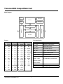
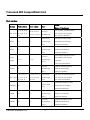
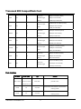
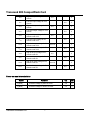
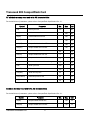
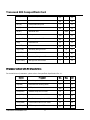
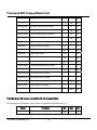
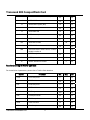
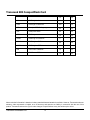
TTrraannsscceenndd 8800X
XC
Coom
mppaaccttFFllaasshh C
Caarrdd
Features
Description
The
Transcend
CF
80X
is
a
High
• RoHS compliant products
Speed
CompactFlash Card with high quality Flash Memory
• Single Power Supply: 5V ± 10% or 3.3V ± 10%
assembled on a printed circuit board.
• Compliant to CompactFlash, PCMCIA, and ATA
standards
• Support PIO mode 0 to PIO mode 6
Placement
• Operating Temperature: 0oC to 70oC
• Storage Temperature: -25oC to 85oC
• On-the-fly ECC
• Host Interface: 8/16-bit access
Flash Interface: 8-bit access
• Endurance: 1,000,000 Program/Erase cycles
A
• Durability of Connector: 10,000 times
• MTBF: 1,000,000 hours
D
B
Transcend Information Inc.
Dimensions
C
1
Side
Millimeters
Inches
A
36.40 ± 0.150
1.43 ± 0.005
B
42.80 ± 0.100
1.69 ± 0.004
C
3.30 ± 0.100
0.13 ± 0.004
D
0.63 ± 0.070
0.02 ± 0.003
TTrraannsscceenndd 8800X
XC
Coom
mppaaccttFFllaasshh C
Caarrdd
Block Diagram
POR
Program memory
(Mask ROM )
RC-OSC
MCU Core
Data memory
(SRAM)
Attribute
Memory
Data Mux
ECC
Flash Interface
CF Interface
Buffer Interface
Buffer Banks
Pinouts
Pin Identification
Pin
Pin
No.
Name
01
Pin
Pin
Symbol
Function
Pin
Pin
Pin
Pin
No. Name
No.
Name
No.
Name
D0 ~ D15
Data Bus (Bi-directional)
VSS
14
A6
27
D11
40
NC
A0 ~ A10
Address Bus (Input)
02
D3
15
A5
28
D12
41
RESET
/CE1,/CE2
Card Enable (Input)
03
D4
16
A4
29
D13
42
/WAIT
/OE, /WE
Output / Write Enable (Input)
04
D5
17
A3
30
D14
43
/INPACK
/REG
Register Select (Input)
05
D6
18
A2
31
D15
44
/REG
/IORD, /IOWR
I/O Access (Input)
06
D7
19
A1
32
/CE2
45
DASP
/IREQ, /IOIS16,
07
/CE1
20
A0
33
VSS
46
PDIAG
RESET, CSEL,
08
A10
21
D0
34
/IORD
47
D8
/INPACK, /WAIT,
09
/OE
22
D1
35
/IOWR
48
D9
DASP, PDIAG
10
A9
23
D2
36
/WE
49
D10
VSS
Ground
11
A8
24 /IOIS16 37
/IREQ
50
VSS
VCC
Vcc Power Input
12
A7
25
VSS
38
VCC
13
VCC
26
VSS
39
CSEL
Transcend Information Inc.
2
I/O Handshaking (Input/Output)
TTrraannsscceenndd 8800X
XC
Coom
mppaaccttFFllaasshh C
Caarrdd
Host interface
Pin Name
Pin No. (100pin)
17, 20, 22, 25, 27,
HA0 ~ HA10
29, 30, 33, 35, 37,
39
HBVD1
HBVD2
HCE1#,
HCE2#
HCSEL#
HD0 ~ HD15
HINPACK#
HIORD#
HIOWR#
43
40
Pin No. (128pin)
Type
20, 25, 29, 33, 35,
5V/3.3V In,
37, 38, 41, 43, 45, 47
Schmitt Trigger
52
48
15, 18
36,
HA0 ~ HA10 (PC Card Memory Mode)
HA0 ~ HA10 (PC Card I/O Mode)
HA0 ~ HA2 (True IDE Mode)
BVD1 (PC Card Memory Mode)
Schmitt Trigger,
STSCHG# (PC Card I/O Mode)
4mA
PDIAG# (True IDE Mode)
5V/3.3V In/Out,
BVD2 (PC Card Memory Mode)
Schmitt Trigger,
SPKR# (PC Card I/O Mode)
4mA
DASP# (True IDE Mode)
Schmitt Trigger,
Pull up
28
(Refer to CF Specification)
5V/3.3V In/Out,
5V/3.3V In,
14, 16
Function
CE1#, CE2# (PC Card Memory Mode)
CE1#, CE2# (PC Card I/O Mode)
Card Enable
CS0#, CS1# (True IDE Mode)
5V/3.3V In,
CSEL# (PC Card Memory Mode)
Schmitt Trigger,
CSEL# (PC Card I/O Mode)
Pull up
CSEL# (True IDE Mode)
1, 2, 3, 4, 5, 7, 9,
1, 2, 3, 4, 5, 7, 9, 11,
5V/3.3V In/Out,
HD0 ~ HD15 (PC Card Memory Mode)
11, 12, 13, 42, 44,
12, 13, 50, 54, 56,
Schmitt Trigger,
HD0 ~ HD15 (PC Card I/O Mode)
45, 47, 48, 50
59, 61, 65
8mA
HD0 ~ HD15 (True IDE Mode)
36
19
21
Transcend Information Inc.
44
23
27
5V/3.3V Output,
4mA
INPACK# (PC Card Memory Mode)
INPACK# (PC Card I/O Mode)
INPACK# (True IDE Mode)
5V/3.3V In,
IORD# (PC Card Memory Mode)
Schmitt Trigger,
IORD# (PC Card I/O Mode)
Pull up
IORD# (True IDE Mode)
5V/3.3V In,
IOWR# (PC Card Memory Mode)
Schmitt Trigger,
IOWR# (PC Card I/O Mode)
Pull up
IOWR# (True IDE Mode)
3
TTrraannsscceenndd 8800X
XC
Coom
mppaaccttFFllaasshh C
Caarrdd
HOE#
18
HRDY
22
26
HREG#
34
38
HRST
46
31
HWAIT#
39
34
HWE#
42
24
HWP
32
49
63
5V/3.3V In,
OE# (PC Card Memory Mode)
Schmitt Trigger,
OE# (PC Card I/O Mode)
Pull up
ATASEL# (True IDE Mode)
5V/3.3V Output,
4mA
RDY/BSY# (PC Card Memory Mode)
IREQ# (PC Card I/O Mode)
INTRQ (True IDE Mode)
5V/3.3V In,
REG# (PC Card Memory Mode)
Schmitt Trigger,
REG# (PC Card I/O Mode)
Pull up
REG# (True IDE Mode)
5V/3.3V In,
RESET (PC Card Memory Mode)
Schmitt Trigger,
RESET (PC Card I/O Mode)
Pull up
RESET# (True IDE Mode)
5V/3.3V Output,
4mA
WAIT# (PC Card Memory Mode)
WAIT# (PC Card I/O Mode)
IORDY (True IDE Mode)
5V/3.3V In,
WE# (PC Card Memory Mode)
Schmitt Trigger,
WE# (PC Card I/O Mode)
Pull up
WE# (True IDE Mode)
WP (PC Card Memory Mode)
5V/3.3V In,
Schmitt Trigger
IOIS16# (PC Card I/O Mode)
IOIS16# (True IDE Mode)
Flash interface
Pin Name
Pin No. (100)
Type
Function
54, 55, 56, 57, 58,
FD0 ~ FD15
59, 60, 61, 63, 66,
Flash Data Bus 0 ~ 7. Connect to flash memory
In/Out, 3mA
pins FD0 ~ FD7.
67, 68, 69, 70, 71, 72
FALE
90
Out, 3mA
FCLE
89
Out, 3mA
Transcend Information Inc.
Flash Address Latch Enable. Connect to flash
memory pin ALE
Flash Command Latch Enable. Connect to flash
memory pin CLE
4
TTrraannsscceenndd 8800X
XC
Coom
mppaaccttFFllaasshh C
Caarrdd
FRE#, FWE#
88 , 91
FCE0# ~
73, 74, 75, 76, 80,
FCE7#
81, 82, 83
FCE8# ~
pin RE/WE.
Flash Chip Enable. Connect to flash memory pin
Out, 2mA
-
Out, 2mA
FWP#
92
Out, 3mA
FRDY
87
In
FCE15#
Flash Read/Write Enable. Connect to flash memory
Out, 3mA
CE.
Flash Chip Enable. Connect to flash memory pin
CE.
Flash Write-Protect. Connect to flash memory pin
WP.
Flash Ready/BSY signal. Connect to flash memory
pin Ready/Busy#.
System interface & power pins
Pin Name
Pin No. (100)
Type
Function
SEL_CLK
86
In
SEL_RST
77
In
TEST
79
In
Test mode enable pin. Connected to GND.
RX
-
In
Test pin. Connected to 3.3V or GND.
TX
-
Out, 3mA
CLKI
94
In
Connected to 3.3V to select internal oscillator, or
GND for external clock.
Connected to 3.3V to select internal power-on-reset
or GND for external reset
Test pin. Not connected.
Clock input
Reset input if reset is provided externally. If
RESET#
97
In
SEL_RST is high, this pin is connected to GND
through a capacitor.
Connected to the same power source as VDDA
ROSC
99
Analog In
REG_EN
-
In
Regulator enable
IROM_SEL
-
In
Test pin. Connected to 3.3V or NC.
VDDPQ
10, 41
GNDPQ
8, 23, 46
VDDQ
64, 85
3.3V power for flash interface
GNDQ
62, 84
Ground for flash interface
Transcend Information Inc.
through a resistor to configure oscillator frequency
Power for CF interface (3.3V or 5V)
Ground for CF interface
5
TTrraannsscceenndd 8800X
XC
Coom
mppaaccttFFllaasshh C
Caarrdd
VDDC
15, 65,
3.3V power for core
GNDC
6, 32, 78
VDD5
52
VDD3
53
GNDR
51
Ground for LDO regulator
VDDA
98
3.3V power for reset circuit
GNDA
100
Ground for analog circuit
VDDCLK
96
3.3V power for oscillator
GNDCLK
93
Ground for oscillator
Ground for core
Power input for LDO regulator (3.3V or 5V)
O
3.3V LDO regulator output
Electrical specifications
Absolute maximum ratings
Symbol
Description
Value
Unit
Notes
VCC
VCC Voltage
- 0.3 to +6.5
V
VDDPQ
VDD
VDD Voltage
- 0.3 to +4.6
V
VDDC, VDDQ
- 0.3 to VCC + 0.3
V
CF interface
- 0.3 to VDD + 0.3
V
Other I/O except CF interface
- 25 to +125
°C
VIN, VOUT
VIN, VOUT
Tstg
All input/output voltages
Storage temperature range
Recommended operating conditions
Symbol
Parameter
VCC
VCC voltage
VDD
VDD voltage
TOPR
Operating temperature
Min.
Typ.
Max.
Unit
4.5
5
5.5
V
3.15
3.3
3.45
V
3.15
3.3
3.45
0
70
V
o
C
DC characteristics
Symbol
Transcend Information Inc.
Parameter
Min.
6
Typ.
Max.
Unit
TTrraannsscceenndd 8800X
XC
Coom
mppaaccttFFllaasshh C
Caarrdd
VIH3
High level input voltage for 3.3V
domain
VIL3
Low level input voltage for 3.3V
domain
VOH3
High level output voltage for 3.3V
domain
VOL3
Low level output voltage for 3.3V
domain
VIH53
High level input voltage for 5V
domain under 3.3V
VIL53
Low level input voltage for 5V
domain under 3.3V
VOH53
High level output voltage for 5V
domain under 3.3V
VOL53
Low level output voltage for 5V
domain under 3.3V
VIH55
High level input voltage for 5V
domain under 5V
VIL55
Low level input voltage for 5V
domain under 5V
VOH55
High level output voltage for 5V
domain under 5V
VOL55
Low level output voltage for 5V
domain under 5V
2.4
V
0.6
2.4
V
V
0.4
2.4
V
V
0.6
Vcc-0.8
V
V
0.4
4.0
V
V
0.8
Vcc-0.8
V
V
0.4
V
Typ.
Unit
Power-on-reset characteristics
Symbol
Parameter
VT(POR)
Threshold voltage of power-on-reset
2.8
V
VT(BOR)
Threshold voltage for brown-out-reset
2.6
V
Transcend Information Inc.
7
TTrraannsscceenndd 8800X
XC
Coom
mppaaccttFFllaasshh C
Caarrdd
CF attribute memory read and write AC characteristics
For the definitions of parameters, please refer to CompactFlash Specification Rev. 2.1.
Symbol
Parameter
Min.
Max.
300
Unit
Ns
tcR
Read cycle time
ta(A)
Address access time
300
Ns
ta(CE)
Card Enable access time
300
ns
ta(OE)
Output Enable access time
150
ns
tdis(CE)
Output disable time from CE
100
ns
tdis(OE)
Output disable time from OE
100
ns
tsu(A)
Address setup time
30
ns
ten(CE)
Output enable time from CE
5
ns
ten(OE)
Output enable time from OE
5
ns
tv(A)
Data valid time from address change
0
ns
tcW
Write cycle time
250
ns
tw(WE)
Write pulse width
150
ns
trec(WE)
Write recovery time
30
ns
tsu(D-WEH)
Data setup time for WE
80
ns
th(D)
Data hold time
30
ns
Common memory read and write AC characteristics
For the definitions of parameters, please refer to CompactFlash Specification Rev. 2.1.
Symbol
Parameter
Min.
Max.
Unit
ta(OE)
Output Enable access time
125
ns
tdis(OE)
Output disable time from OE
100
ns
Transcend Information Inc.
8
TTrraannsscceenndd 8800X
XC
Coom
mppaaccttFFllaasshh C
Caarrdd
tsu(A)
Address setup time
30
ns
th(A)
Address hold time
20
ns
tsu(CE)
Card Enable setup time
9
ns
th(CE)
Card Enable hold time
20
ns
tw(WT)
Wait width time
tw(WE)
Write pulse time
150
ns
tsu(D-WEH)
Data setup time for WE
80
ns
th(D)
Data hold time
30
ns
trec(WE)
Write recover time
30
ns
tv(WT-OE)
Wait delay falling from OE
35
ns
tv(D-WT)
Data setup for wait release
0
Ns
tv(WT-WE1)
Wait delay falling from WE
35
ns
tv(WT-WE2)
WE high from wait release
3000
0
ns
ns
I/O access read and write AC characteristics
For the definitions of parameters, please refer to CompactFlash Specification Rev. 2.1.
Symbol
Parameter
td(IORD)
Data delay after IORD
th(IORD)
Data hold time following IORD
tw(IORD)
Min.
Max.
Unit
100
ns
0
ns
IORD pulse width
165
ns
tsuA(IORD)
Address setup time for IORD
70
ns
thA(IORD)
Address hold time from IORD
20
ns
tsuCE(IORD)
Card Enable setup time for IORD
5
ns
thCE(IORD)
Card Enable hold time from IORD
20
ns
tsuREG(IORD)
REG setup time for IORD
5
ns
Transcend Information Inc.
9
TTrraannsscceenndd 8800X
XC
Coom
mppaaccttFFllaasshh C
Caarrdd
thREG(IORD)
REG hold time from IORD
0
tdfINP(IORD)
INPACK delay falling from IORD
0
tdrINP(IORD)
ns
45
ns
INPACK delay rising from IORD
45
ns
tdfIO16(IORD)
IOIS16 delay falling from address
35
ns
tdrIO16(IORD)
IOIS16 delay rising from address
35
ns
tdWT(IORD)
Wait delay falling from IORD
35
ns
td(WT)
Data delay from wait rising
0
ns
tsu(IOWR)
Data setup time for IOWR
60
ns
th(IOWR)
Data hold time from IOWR
30
ns
tw(IOWR)
IOWR pulse width
165
ns
tsuA(IOWR)
Address setup time for IOWR
70
ns
thA(IOWR)
Address hold time from IOWR
20
ns
tsuCE(IOWR)
Card Enable setup time for IOWR
5
ns
thCE(IOWR)
Card Enable hold time from IOWR
20
ns
tsuREG(IOWR)
REG setup time for IOWR
5
ns
thREG(IOWR)
REG hold time from IOWR
0
ns
tdWT(IOWR)
Wait delay falling from IOWR
tdrIOWR(WT)
IOWR high from wait high
tw(WT)
Wait width time
35
0
ns
ns
3000
ns
Max.
Unit
True-IDE mode I/O access read and write AC characteristics
For the definitions of parameters, please refer to CompactFlash Specification Rev. 2.1.
Symbol
t0
Transcend Information Inc.
Parameter
Min.
120
Cycle time
10
ns
TTrraannsscceenndd 8800X
XC
Coom
mppaaccttFFllaasshh C
Caarrdd
t1
Address valid to IORD/IOWR setup
25
ns
t2
IORD/IOWR
70
ns
t2
IORD/IOWR register (8bit)
70
ns
t3
IOWR data setup
20
ns
t4
IOWR data hold
10
ns
t5
IORD data setup
20
ns
t6
IORD data hold
5
ns
t6Z
30
IORD data tri-state
ns
IORD/IOWR to address valid hold
10
ns
Read data valid to IORDY active, if IORDY
initially low after tA
0
ns
tA
IORDY setup time
35
ns
tB
IORDY pulse width
tC
IORDY assertion to release
t9
tRD
1250
ns
5
ns
Max.
Unit
Read/write timing for NAND type flash
For the definition of parameters, please refer to Toshiba flash datasheet
Symbol
Parameter
Min.
tCLS
FCLE setup time
0
ns
tCLH
FCLE hold time
10
ns
tCS
FCE# setup time
0
ns
tCH
FCE# hold time
10
ns
tCEH
FCE# high hold time
100
ns
tWP
FWE# pulse width
25
ns
tALS
FALE setup time
0
ns
tALH
FALE hold time
10
ns
tDS
Data Setup time
20
ns
Transcend Information Inc.
11
TTrraannsscceenndd 8800X
XC
Coom
mppaaccttFFllaasshh C
Caarrdd
tDH
Data hold time
10
ns
tWH
FWE# high hold time
15
ns
tWW
FWP high to FWE# low
100
ns
tRR
Ready-to-FRE# Falling edge
20
ns
tRP
FRE# pulse width
25
ns
tREH
FRE# high hold time
15
ns
tRHW
FRE# high to FWE# low
0
ns
tWHC
FWE# high to FCE# low
30
ns
tWHR
FWE# high to FRE# low
60
ns
tAR
FALE low to FRE# low
10
ns
tCLR
FCLE low to FRE# low
10
ns
Above technical information is based on industry standard data and tested to be reliable. However, Transcend makes no
warranty, either expressed or implied, as to its accuracy and assumes no liability in connection with the use of this
product. Transcend reserves the right to make changes in specifications at any time without prior notice.
Transcend Information Inc.
12