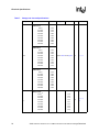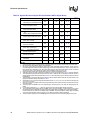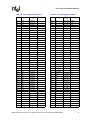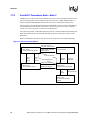
1
Intel® Celeron® Processor on
0.13 Micron Process in the
478-Pin Package
Datasheet
■
■
■
■
■
■
■
Available at 2 GHz, 2.10 GHz, 2.20 GHz,
2.30 GHz, 2.40 GHz, 2.50 GHz, 2.60 GHz,
2.70 GHz, and 2.80 GHz
Binary compatible with applications
running on previous members of the Intel
microprocessor line
System bus frequency at 400 MHz
Rapid Execution Engine: Arithmetic Logic
Units (ALUs) run at twice the processor
core frequency
Hyper Pipelined Technology
Advanced Dynamic Execution
— Very deep out-of-order execution
— Enhanced branch prediction
8-KB Level 1 data cache
■
■
■
■
■
Level 1 Execution Trace Cache stores 12K
micro-ops and removes decoder latency
from main execution loops
128-KB Advanced Transfer Cache (on-die,
full speed Level 2 (L2) cache) with Error
Correction Code (ECC)
144 Streaming SIMD Extensions 2 (SSE2)
Instructions
Power Management capabilities
— System Management mode
— Multiple low-power states
Optimized for 32-bit applications running
on advanced 32-bit operating systems
The Intel® Celeron® processor on 0.13 micron process in the 478-pin package expands Intel’s
processor family into the value-priced PC market segment. Celeron processors provide the value
customer the capability to get onto the Internet affordably, and use educational programs, homeoffice software and productivity applications. All of the Celeron processors include an integrated
L2 cache, and are built on Intel's advanced CMOS process technology. The Celeron processor is
backed by over 30 years of Intel experience in manufacturing high-quality, reliable
microprocessors.
November 2003
Document Number: 251748-007
INFORMATION IN THIS DOCUMENT IS PROVIDED IN CONNECTION WITH INTEL® PRODUCTS. NO LICENSE, EXPRESS OR IMPLIED, BY
ESTOPPEL OR OTHERWISE, TO ANY INTELLECTUAL PROPERTY RIGHTS IS GRANTED BY THIS DOCUMENT. EXCEPT AS PROVIDED IN
INTEL'S TERMS AND CONDITIONS OF SALE FOR SUCH PRODUCTS, INTEL ASSUMES NO LIABILITY WHATSOEVER, AND INTEL DISCLAIMS
ANY EXPRESS OR IMPLIED WARRANTY, RELATING TO SALE AND/OR USE OF INTEL PRODUCTS INCLUDING LIABILITY OR WARRANTIES
RELATING TO FITNESS FOR A PARTICULAR PURPOSE, MERCHANTABILITY, OR INFRINGEMENT OF ANY PATENT, COPYRIGHT OR OTHER
INTELLECTUAL PROPERTY RIGHT. Intel products are not intended for use in medical, life saving, or life sustaining applications.
Intel may make changes to specifications and product descriptions at any time, without notice.
Designers must not rely on the absence or characteristics of any features or instructions marked “reserved” or “undefined.” Intel reserves these for
future definition and shall have no responsibility whatsoever for conflicts or incompatibilities arising from future changes to them.
The Intel® Celeron® processor may contain design defects or errors known as errata which may cause the product to deviate from published
specifications. Current characterized errata are available on request.
Contact your local Intel sales office or your distributor to obtain the latest specifications and before placing your product order.
Intel, Celeron, Pentium, and the Intel logo are trademarks or registered trademarks of Intel Corporation or its subsidiaries in the United States and
other countries.
*Other names and brands may be claimed as the property of others.
Copyright © 2002–2003, Intel Corporation
2
Intel® Celeron® Processor on 0.13 Micron Process in the 478-Pin Package Datasheet
Contents
1
Introduction .................................................................................................................. 9
1.1
1.2
2
Electrical Specifications ........................................................................................13
2.1
2.2
2.3
2.4
2.5
2.6
2.7
2.8
2.9
2.10
2.11
2.12
2.13
2.14
3
System Bus and GTLREF ...................................................................................13
Power and Ground Pins ......................................................................................13
Decoupling Guidelines ........................................................................................13
2.3.1 VCC Decoupling .....................................................................................14
2.3.2 System Bus AGTL+ Decoupling.............................................................14
2.3.3 System Bus Clock (BCLK[1:0]) and Processor Clocking .......................14
Voltage Identification ...........................................................................................15
2.4.1 Phase Lock Loop (PLL) Power and Filter...............................................16
Reserved, Unused Pins, and TESTHI[12:0]........................................................18
System Bus Signal Groups .................................................................................19
Asynchronous GTL+ Signals...............................................................................20
Test Access Port (TAP) Connection....................................................................20
System Bus Frequency Select Signals (BSEL[1:0])............................................20
Maximum Ratings................................................................................................21
Processor DC Specifications...............................................................................21
2.11.1 Flexible Motherboard Guidelines (FMB).................................................21
AGTL+ System Bus Specifications .....................................................................28
System Bus AC Specifications ............................................................................29
Processor AC Timing Waveforms .......................................................................32
System Bus Signal Quality Specifications ....................................................41
3.1
3.2
3.3
4
Terminology........................................................................................................... 9
1.1.1 Processor Packaging Terminology.........................................................10
References ..........................................................................................................11
System Bus Clock (BCLK) Signal Quality Specifications ....................................41
System Bus Signal Quality Specifications and Measurement Guidelines...........42
System Bus Signal Quality Specifications and Measurement Guidelines...........45
3.3.1 Overshoot/Undershoot Guidelines .........................................................45
3.3.2 Overshoot/Undershoot Magnitude .........................................................45
3.3.3 Overshoot/Undershoot Pulse Duration...................................................45
3.3.4 Activity Factor .........................................................................................46
3.3.5 Reading Overshoot/Undershoot Specification Tables............................46
3.3.6 Conformance Determination to Overshoot/Undershoot
Specifications .........................................................................................47
Package Mechanical Specifications .................................................................51
4.1
4.2
4.3
4.4
4.5
Package Load Specifications ..............................................................................54
Processor Insertion Specifications ......................................................................55
Processor Mass Specifications ...........................................................................55
Processor Materials.............................................................................................55
Processor Markings.............................................................................................55
Intel® Celeron® Processor on 0.13 Micron Process in the 478-Pin Package Datasheet
3
5
Pin Listing and Signal Definitions..................................................................... 59
5.1
5.2
6
Thermal Specifications and Design Considerations ................................. 81
6.1
7
7.3
8.3
8.4
Introduction ......................................................................................................... 91
Mechanical Specifications................................................................................... 92
8.2.1 Boxed Processor Cooling Solution Dimensions ..................................... 92
8.2.2 Boxed Processor Fan Heatsink Weight.................................................. 93
8.2.3 Boxed Processor Retention Mechanism and Heatsink Assembly.......... 93
Electrical Requirements ...................................................................................... 94
8.3.1 Fan Heatsink Power Supply ................................................................... 94
Thermal Specifications........................................................................................ 97
8.4.1 Boxed Processor Cooling Requirements ............................................... 97
8.4.2 Variable Speed Fan ............................................................................... 98
Debug Tools Specifications............................................................................... 101
9.1
4
Power-On Configuration Options ........................................................................ 85
Clock Control and Low Power States.................................................................. 85
7.2.1 Normal State—State 1 ........................................................................... 85
7.2.2 AutoHALT Powerdown State—State 2 .................................................. 86
7.2.3 Stop-Grant State—State 3 ..................................................................... 87
7.2.4 HALT/Grant Snoop State—State 4 ........................................................ 87
7.2.5 Sleep State—State 5.............................................................................. 88
Thermal Monitor .................................................................................................. 88
7.3.1 Thermal Diode........................................................................................ 90
Boxed Processor Specifications ....................................................................... 91
8.1
8.2
9
Processor Thermal Specifications....................................................................... 82
6.1.1 Thermal Specifications ........................................................................... 82
6.1.2 Thermal Metrology ................................................................................. 83
6.1.2.1 Processor Case Temperature Measurement ............................ 83
Features ....................................................................................................................... 85
7.1
7.2
8
Processor Pin Assignments ................................................................................ 59
Alphabetical Signals Reference .......................................................................... 72
Logic Analyzer Interface (LAI)........................................................................... 101
9.1.1 Mechanical Considerations .................................................................. 101
9.1.2 Electrical Considerations...................................................................... 101
Intel® Celeron® Processor on 0.13 Micron Process in the 478-Pin Package Datasheet
Figures
1
2
3
4
5
6
7
8
9
10
11
12
13
14
15
16
17
18
19
20
21
22
23
24
25
26
27
28
29
30
31
32
33
34
35
36
37
38
39
40
41
42
43
44
45
VCCVID Pin Voltage and Current Requirements ................................................15
Typical VCCIOPLL, VCCA and VSSA Power Distribution ..................................17
Phase Lock Loop (PLL) Filter Requirements ......................................................17
VCC Static and Transient Tolerance...................................................................24
ITPCLKOUT[1:0] Output Buffer Diagram ............................................................27
AC Test Circuit ....................................................................................................32
TCK Clock Waveform..........................................................................................33
Differential Clock Waveform................................................................................33
Differential Clock Crosspoint Specification..........................................................34
System Bus Common Clock Valid Delay Timings...............................................34
System Bus Reset and Configuration Timings....................................................35
Source Synchronous 2X (Address) Timings .......................................................35
Source Synchronous 4X Timings ........................................................................36
Power Up Sequence ...........................................................................................37
Power Down Sequence.......................................................................................37
Test Reset Timings .............................................................................................38
THERMTRIP# Power Down Sequence...............................................................38
ITPCLKOUT Valid Delay Timing .........................................................................38
FERR#/PBE# Valid Delay Timing .......................................................................39
TAP Valid Delay Timing ......................................................................................39
BCLK Signal Integrity Waveform.........................................................................42
Low-to-High System Bus Receiver Ringback Tolerance.....................................43
High-to-Low System Bus Receiver Ringback Tolerance.....................................43
Low-to-High System Bus Receiver Ringback Tolerance for PWRGOOD
and TAP Buffers ..................................................................................................44
High-to-Low System Bus Receiver Ringback Tolerance for PWRGOOD
and TAP Buffers ..................................................................................................44
Maximum Acceptable Overshoot/Undershoot Waveform ...................................49
Exploded View of Processor Components on a System Board ..........................51
Processor Package .............................................................................................52
Processor Cross-Section and Keep-In ................................................................53
Processor Pin Detail............................................................................................53
IHS Flatness Specification ..................................................................................54
Processor Markings.............................................................................................55
Processor Pinout Coordinates (Top View, Left Side) ..........................................56
Processor Pinout Coordinates (Top View, Right Side)........................................57
Example Thermal Solution (Not to Scale) ...........................................................81
Guideline Locations for Case Temperature (TC) Thermocouple Placement ......83
Stop Clock State Machine ...................................................................................86
Mechanical Representation of the Boxed Processor ..........................................91
Side View Space Requirements for the Boxed Processor ..................................92
Top View Space Requirements for the Boxed Processor ...................................93
Boxed Processor Fan Heatsink Power Cable Connector Description.................95
MotherBoard Power Header Placement Relative to Processor Socket ..............96
Boxed Processor Fan Heatsink Airspace Keep-Out Requirements
(Side 1 View) .......................................................................................................97
Boxed Processor Fan Heatsink Airspace Keep-Out Requirements
(Side 2 View) .......................................................................................................98
Boxed Processor Fan Heatsink Set Points .........................................................99
Intel® Celeron® Processor on 0.13 Micron Process in the 478-Pin Package Datasheet
5
Tables
1
2
3
4
5
6
7
8
9
10
11
12
13
14
15
16
17
18
19
20
21
22
23
24
25
26
27
28
29
30
31
32
33
34
35
36
37
38
39
40
41
42
6
References.......................................................................................................... 11
VCCVID Pin Voltage Requirements.................................................................... 15
Voltage Identification Definition........................................................................... 16
System Bus Pin Groups ...................................................................................... 19
BSEL[1:0] Frequency Table for BCLK[1:0] ......................................................... 20
Processor DC Absolute Maximum Ratings ......................................................... 21
Voltage and Current Specifications..................................................................... 22
VCC Static and Transient Tolerance................................................................... 23
System Bus Differential BCLK Specifications ..................................................... 25
AGTL+ Signal Group DC Specifications ............................................................. 25
Asynchronous GTL+ Signal Group DC Specifications ........................................ 26
PWRGOOD and TAP Signal Group DC Specifications ...................................... 26
ITPCLKOUT[1:0] DC Specifications.................................................................... 27
BSEL [1:0] and VID[4:0] DC Specifications......................................................... 27
AGTL+ Bus Voltage Definitions........................................................................... 28
System Bus Differential Clock Specifications...................................................... 29
System Bus Common Clock AC Specifications .................................................. 29
System Bus Source Synch AC Specifications AGTL+ Signal Group .................. 30
Miscellaneous Signals AC Specifications ........................................................... 31
System Bus AC Specifications (Reset Conditions) ............................................. 31
TAP Signals AC Specifications ........................................................................... 31
ITPCLKOUT[1:0] AC Specifications.................................................................... 32
BCLK Signal Quality Specifications .................................................................... 41
Ringback Specifications for AGTL+ and Asynchronous GTL+ Signals
Groups ................................................................................................................ 42
Ringback Specifications for PWRGOOD Input and TAP Signal Group .............. 43
1.525V VID Source Synchronous (400 MHz) AGTL+ Signal Group
Overshoot/Undershoot Tolerance ....................................................................... 47
1.525 V VID Source Synchronous (200 MHz) AGTL+ Signal Group
Overshoot/Undershoot Tolerance ....................................................................... 48
1.525 V VID Common Clock (100 MHz) AGTL+ Signal Group
Overshoot/Undershoot Tolerance ....................................................................... 48
1.525 V VID Asynchronous GTL+, PWRGOOD Input, and TAP Signal
Group Overshoot/Undershoot Tolerance ............................................................ 48
Description Table for Processor Dimensions ...................................................... 52
Package Dynamic and Static Load Specifications .............................................. 54
Processor Mass .................................................................................................. 55
Processor Material Properties............................................................................. 55
Pin Listing by Pin Name ...................................................................................... 60
Pin Listing by Pin Number................................................................................... 66
Signal Description ............................................................................................... 72
Processor Thermal Design Power ...................................................................... 83
Power-On Configuration Option Pins .................................................................. 85
Thermal Diode Parameters ................................................................................. 90
Thermal Diode Interface...................................................................................... 90
Fan Heatsink Power and Signal Specifications................................................... 95
Boxed Processor Fan Heatsink Set Points ......................................................... 99
Intel® Celeron® Processor on 0.13 Micron Process in the 478-Pin Package Datasheet
Revision History
Revision
Description
Date
-002
Updated document with 2.10 GHz and 2.20 GHz specifications.
November 2002
-003
Added 2.30 GHz and 2.40 GHz specifications.
March 2003
-004
Added 2.50 GHz and 2.60 GHz specifications. Updated thermal
specifications and thermal monitor sections. Updated PROCHOT# pin
definition.
June 2003
-005
Updated Title page.
August 2003
-006
Added 2.70 GHz specifications. Updated Table 20 and Figure 11.
September 2003
-007
Added 2.80 GHz specifications. Updated Table 19.
November 2003
Intel® Celeron® Processor on 0.13 Micron Process in the 478-Pin Package Datasheet
7
This page is intentionally left blank.
8
Intel® Celeron® Processor on 0.13 Micron Process in the 478-Pin Package Datasheet
Introduction
Introduction
1
The Intel® Celeron® processor on 0.13 micron process and in the 478-pin package uses Flip-Chip
Pin Grid Array (FC-PGA2) package technology, and plugs into a 478-pin surface mount, Zero
Insertion Force (ZIF) socket, referred to as the mPGA478B socket. The Celeron processor on
0.13 micron process maintains the tradition of compatibility with IA-32 software. In this
document, the Celeron processor on 0.13 micron process may be referred to as the “Celeron
processor” or simply “the processor.”
The Celeron processor on 0.13 micron process is designed for uni-processor based Value PC
desktop systems. Features of the processor include hyper pipelined technology, a 400 MHz system
bus, and an execution trace cache. The 400 MHz system bus is a quad-pumped bus running off a
100 MHz system clock making 3.2 GB/s data transfer rates possible. The execution trace cache is a
first level cache that stores approximately 12k decoded micro-operations, which removes the
decoder from the main execution path.
Additional features include advanced dynamic execution, advanced transfer cache, enhanced
floating point and multi-media unit, and Streaming SIMD Extensions 2 (SSE2). The advanced
dynamic execution improves speculative execution and branch prediction internal to the processor.
The advanced transfer cache is a 128 KB, on-die level 2 (L2) cache. The floating point and multimedia units have 128-bit wide registers with a separate register for data movement. SSE2 support
includes instructions for double-precision floating point, SIMD integer, and memory management.
Power management capabilities such as AutoHALT, Stop-Grant, and Sleep have been retained.
The Celeron processor on 0.13 micron process 400 MHz system bus uses a split-transaction,
deferred reply protocol. This system bus is not compatible with the P6 processor family bus. The
400 MHz system bus uses Source-Synchronous Transfer (SST) of address and data to improve
throughput by transferring data four times per bus clock (4X data transfer rate, as in AGP 4X).
Along with the 4X data bus, the address bus can deliver addresses two times per bus clock, and is
referred to as a “double-clocked” or 2X address bus. Working together, the 4X data bus and 2X
address bus provide a data bus bandwidth of up to 3.2 GB/s.
Intel will be enabling support components for the Celeron processor on 0.13 micron process
including a heatsink, heatsink retention mechanism, and socket. Manufacturability is a high
priority; hence, mechanical assembly can be completed from the top of the motherboard and should
not require any special tooling. The processor system bus uses a variant of GTL+ signalling
technology called Assisted Gunning Transceiver Logic (AGTL+) signalling technology.
The processor includes an address bus powerdown capability which removes power from the
address and data pins when the system bus is not in use. This feature is always enabled on the
processor.
1.1
Terminology
A ‘#’ symbol after a signal name refers to an active low signal, indicating that the signal is in the
active state when driven to a low level. For example, when RESET# is low, a reset has been
requested. Conversely, when NMI is high, a nonmaskable interrupt has occurred. In the case of
signals where the name does not imply an active state but describes part of a binary sequence
(such as address or data), the ‘#’ symbol implies that the signal is inverted. For example,
D[3:0] = ‘HLHL’ refers to a hex ‘A’, and D[3:0]# = ‘LHLH’ also refers to a hex ‘A’ (H= High logic
level, L= Low logic level).
Intel® Celeron® Processor on 0.13 Micron Process in the 478-Pin Package Datasheet
9
Introduction
“System Bus” refers to the interface between the processor and system core logic (the chipset
components). The system bus is a multiprocessing interface to processors, memory, and I/O.
1.1.1
Processor Packaging Terminology
The following are commonly used terms:
• Intel® Celeron® processor on 0.13 micron process and in the 478-pin package (also
referred as the Intel® Celeron® processor on 0.13 micron process or processor) —
0.13 micron processor core in the 478-pin FC-PGA2 package with a 128-KB L2 cache.
• Intel£ Celeron£ processor in the 478-pin package — 0.18 micron processor core in the
478-pin FC-PGA2 package with a 128-KB L2 cache.
• Intel£ Pentium£ 4 processor with 512-KB L2 cache on 0.13 micron process —
0.13 micron process version of Pentium 4 processor in the 478-pin FC-PGA2 package with a
512-KB L2 cache.
• Processor — For this document, the term processor means Celeron processor on 0.13 micron
process.
• Keep-Out Zone — The area on or near the processor that system design can not use. This area
must be kept free of all components to make room for the processor package, retention
mechanism, heatsink, and heatsink clips.
• Intel® 850 chipset — Chipset that supports RDRAM* memory technology for Celeron
processor on 0.13 micron process.
• Intel® 845 chipset — Chipset that supports PC133 and DDR memory technology for the
Celeron processor on 0.13 micron process.
• Intel® 845G chipset — Chipset with embedded graphics that supports DDR memory
technology for the Celeron processor on 0.13 micron process.
• Intel® 845E chipset — Chipset that supports DDR memory technology for the Celeron
processor on 0.13 micron process.
• Processor core — Celeron processor on 0.13 micron process core die with integrated
L2 cache.
• FC-PGA2 package — Flip-Chip Pin Grid Array package with 50-mil pin pitch and Integrated
Heat Spreader.
• mPGA478B socket — Surface mount, 478 pin, Zero Insertion Force (ZIF) socket with 50-mil
pin pitch. The socket mates the processor to the system board.
• Integrated heat spreader — The surface used to make contact between a heatsink or other
thermal solution and the processor. Abbreviated IHS.
• Retention mechanism — The structure mounted on the system board that provides support
and retention of the processor heatsink.
10
Intel® Celeron® Processor on 0.13 Micron Process in the 478-Pin Package Datasheet
Introduction
1.2
References
The following documents should be referenced for additional information:
Table 1.
References
Document
Intel®
Intel®
Pentium®
Document Number/Source
4 Processor in the 478 Pin Package and
850 Chipset Platform Design Guide
http://developer.intel.com/design/
pentium4/guides/249888.htm
Intel® Pentium® 4 Processor in the 478 Pin Package and
Intel® 845 Chipset Platform for DDR Design Guide
http://developer.intel.com/design/
chipsets/designex/298605.htm
Intel® Pentium® 4 Processor in the 478 Pin Package and
Intel® 845 Chipset Platform for SDR Design Guide
http://developer.intel.com/design/
pentium4/guides/298354.htm
Intel® Pentium® 4 Processor in the 478 Pin Package and
Intel® 845E Chipset Platform for DDR Design Guide
http://developer.intel.com/design/
chipsets/designex/298653.htm
Intel® Pentium® 4 Processor in 478-pin Package and
Intel® 845G/845GL Chipset Platform Design Guide
http://developer.intel.com/design/
chipsets/designex/298654.htm
Intel® Pentium® 4 Processor in the 478-pin Package Thermal Design
Guidelines
http://developer.intel.com/design/
pentium4/guides/249889.htm
Intel® Pentium® 4 Processor VR-Down Design Guidelines
http://developer.intel.com/design/
Pentium4/guides/249891.htm
Intel® Pentium® 4 Processor 478-pin Socket (mPGA478B) Design
Guidelines
http://developer.intel.com/design/
pentium4/guides/249890.htm
Intel® Pentium® 4 Processor CK00 Clock Synthesizer/Driver Design
Guidelines
http://developer.intel.com/design/
pentium4/guides/249206.htm
CK408 Clock Design Guidelines
Contact Intel field representative.
Intel®
IA-32
Architecture Software Developer’s Manual,
Volume 1: Basic Architecture
http://developer.intel.com/design/
pentium4/manuals/245470.htm
IA-32 Intel® Architecture Software Developer’s Manual,
Volume 2: Instruction Set Reference
http://developer.intel.com/design/
pentium4/manuals/245471.htm
IA-32 Intel® Architecture Software Developer’s Manual,
Volume 3: System Programming Guide
http://developer.intel.com/design/
pentium4/manuals/245472.htm
ITP700 Debug Port Design Guide
http://developer.intel.com/design/
Xeon/guides/249679.htm
AP-485 Intel® Processor Identification and the CPUID Instruction
http://developer.intel.com/design/
xeon/applnots/241618.htm
Intel® Celeron® Processor on 0.13 Micron Process in the 478-Pin Package Datasheet
11
Introduction
This page is intentionally left blank.
12
Intel® Celeron® Processor on 0.13 Micron Process in the 478-Pin Package Datasheet
Electrical Specifications
Electrical Specifications
2.1
2
System Bus and GTLREF
Most Celeron processor on 0.13 micron process system bus signals use Assisted Gunning
Transceiver Logic (AGTL+) signalling technology. As with the P6 family of microprocessors, this
signalling technology provides improved noise margins and reduced ringing through low voltage
swings and controlled edge rates. Like the Intel£ Pentium£ 4 processor, the termination voltage
level for the Celeron processor on 0.13 micron process AGTL+ signals is VCC, which is the
operating voltage of the processor core. The use of a termination voltage that is determined by the
processor core allows better voltage scaling on the system bus for Celeron processor on
0.13 micron process. Because of the speed improvements to data and address bus, signal integrity
and platform design methods have become more critical than with previous processor families.
Design guidelines for the Celeron processor on 0.13 micron process system bus are described in the
appropriate Platform Design Guide (refer to Table 1).
The AGTL+ inputs require a reference voltage (GTLREF) that is used by the receivers to determine
whether a signal is a logical 0 or a logical 1. GTLREF must be generated on the system board.
Termination resistors are provided on the processor silicon, and are terminated to the processor
core voltage (VCC). Intel chipsets also provide on-die termination, thus eliminating the need to
terminate most AGTL+ signals on the system board.
Some AGTL+ signals do not include on-die termination and must be terminated on the system
board. See Table 4 for details regarding these signals.
The AGTL+ bus depends on incident wave switching. Therefore, timing calculations for AGTL+
signals are based on flight time as opposed to capacitive deratings. Analog signal simulation of the
system bus, including trace lengths, is highly recommended when designing a system.
2.2
Power and Ground Pins
For clean on-chip power distribution, the Celeron processor on 0.13 micron process has 85 VCC
(power) and 181 VSS (ground) inputs. All power pins must be connected to VCC, and all VSS pins
must be connected to a system ground plane.The processor VCC pins must be supplied with the
voltage defined by the VID (Voltage ID) pins and the loadline specifications (see Figure 4).
2.3
Decoupling Guidelines
Because of the large number of transistors and high internal clock speeds, the processor is capable
of generating large average current swings between low and full power states. This may cause
voltages on power planes to sag below their minimum values if bulk decoupling is not adequate.
Care must be taken in the board design to ensure that the voltage provided to the processor remains
within the specifications listed in Table 7. Failure to do so can result in timing violations and/or
affect the long term reliability of the processor. For further information and design guidelines, refer
to Table 1 for the appropriate Platform Design Guide, and the Intel£ Pentium£ 4 Processor
VR-Down Design Guidelines.
Intel® Celeron® Processor on 0.13 Micron Process in the 478-Pin Package Datasheet
13
Electrical Specifications
2.3.1
VCC Decoupling
Regulator solutions must provide bulk capacitance with a low Effective Series Resistance (ESR)
and keep a low interconnect resistance from the regulator to the socket. Bulk decoupling for the
large current swings when the part is powering on or is entering or exiting low power states must
be provided by the voltage regulator solution (VR). For design guidelines, refer to Table 1 for the
appropriate Platform Design Guide, and to the Intel£ Pentium£ 4 Processor VR-Down Design
Guidelines.
2.3.2
System Bus AGTL+ Decoupling
The Celeron processor on 0.13 micron process integrates signal termination on the die and
incorporates high frequency decoupling capacitance on the processor package. Decoupling must
also be provided by the system motherboard for proper AGTL+ bus operation. For more
information, refer to the appropriate platform design guide listed in Table 1.
2.3.3
System Bus Clock (BCLK[1:0]) and Processor Clocking
BCLK[1:0] directly control the system bus interface speed as well as the core frequency of the
processor. As in previous generation processors, the Celeron processor on 0.13 micron process core
frequency is a multiple of the BCLK[1:0] frequency.
Like the Celeron processor in the 478-pin package, the Celeron processor on 0.13 micron process
uses a differential clocking implementation. For more information on clocking, refer to the CK408
Clock Design Guidelines and also the CK00 Clock Synthesizer/Driver Design Guidelines.
14
Intel® Celeron® Processor on 0.13 Micron Process in the 478-Pin Package Datasheet
Electrical Specifications
2.4
Voltage Identification
The VID specification for Celeron processor on 0.13 micron process is supported by the Intel£
Pentium£ 4 Processor VR-Down Design Guidelines. The voltage set by the VID pins is the
maximum voltage allowed by the processor. A minimum voltage is provided in Table 7 and
changes with frequency. This allows processors running at a higher frequency to have a relaxed
minimum voltage specification. The specifications have been set such that one voltage regulator
can work with all supported frequencies.
The Celeron processor on 0.13 micron process uses five voltage identification pins, VID[4:0], to
support automatic selection of power supply voltages. The VID pins for the Celeron processor on
0.13 micron process are open drain outputs driven by the processor VID circuitry. The VID signals
rely on pull-up resistors tied to a 3.3 V (max) supply to set the signal to a logic high level. These
pull-up resistors may be either external logic on the motherboard, or internal to the Voltage
Regulator. Table 3 specifies the voltage levels corresponding to the states of VID[4:0]. A 1 in this
table refers to a high voltage level, and a 0 refers to low voltage level. The definition provided in
Table 3 is not related in any way to previous P6 processors or VRs, but is compatible with the
Pentium 4 processor in the 478-pin package. If the processor socket is empty (VID[4:0] = 11111) or
the voltage regulation circuit cannot supply the voltage that is requested, it must disable itself. See
the Intel£ Pentium£ 4 Processor VR-Down Design Guidelines for more details.
Power source characteristics must be stable whenever the supply to the voltage regulator is stable.
Refer to the Figure 14 for timing details of the power up sequence. Also refer to the appropriate
platform design guide listed in Table 1 for implementation details.
The Voltage Identification circuit requires an independent 1.2 V supply. This voltage must be
routed to the processor VCCVID pin. Table 2 and Figure 1 describe the voltage and current
requirements of the VCCVID pin.
Table 2.
VCCVID Pin Voltage Requirements
Symbol
VCCVID
Parameter
VCC for voltage identification circuit.
Min
Typ
Max
Unit
–5%
1.2
+10%
V
Notes
1
NOTES:
This specification applies to both static and transient components. The rising edge of VCCVID must be
monotonic from 0 to 1.1 V. See Figure 1 for current requirements. In this case, monotonic is defined as continuously increasing with less than 50 mV of peak to peak noise for any width greater than 2 ns superimposed on the rising edge.
1.
Figure 1. VCCVID Pin Voltage and Current Requirements
1.2 V + 10%
1.2 V - 5%
1.0 V
VCCVID
VIDs latched
30 mA
1 mA
4 ns
Intel® Celeron® Processor on 0.13 Micron Process in the 478-Pin Package Datasheet
15
Electrical Specifications
Table 3.
Voltage Identification Definition
Processor Pins
Vcc_max
2.4.1
VID4
VID3
VID2
VID1
VID0
1
1
1
1
1
VRM output off
1
1
1
1
0
1.100
1
1
1
0
1
1.125
1
1
1
0
0
1.150
1
1
0
1
1
1.175
1
1
0
1
0
1.200
1
1
0
0
1
1.225
1
1
0
0
0
1.250
1
0
1
1
1
1.275
1
0
1
1
0
1.300
1
0
1
0
1
1.325
1
0
1
0
0
1.350
1
0
0
1
1
1.375
1
0
0
1
0
1.400
1
0
0
0
1
1.425
1
0
0
0
0
1.450
0
1
1
1
1
1.475
0
1
1
1
0
1.500
0
1
1
0
1
1.525
0
1
1
0
0
1.550
Phase Lock Loop (PLL) Power and Filter
VCCA and VCCIOPLL are power sources required by the PLL clock generators on the Celeron
processor on 0.13 micron process. Since these PLLs are analog in nature, they require quiet power
supplies for minimum jitter. Jitter is detrimental to the system—it degrades external I/O timings, as
well as internal core timings (i.e., maximum frequency). To prevent this degradation, these supplies
must be low pass filtered from VCC. A typical filter topology is shown in Figure 2.
The AC low-pass requirements, with input at VCC and output measured across the capacitor
(CA or CIO in Figure 2), is as follows:
•
•
•
•
< 0.2 dB gain in pass band
< 0.5 dB attenuation in pass band < 1 Hz
> 34 dB attenuation from 1 MHz to 66 MHz
> 28 dB attenuation from 66 MHz to core frequency
The filter requirements are illustrated in Figure 3. For recommendations on implementing the filter,
refer to the appropriate Platform Design Guide listed in Table 1.
16
Intel® Celeron® Processor on 0.13 Micron Process in the 478-Pin Package Datasheet
Electrical Specifications
Figure 2. Typical VCCIOPLL, VCCA and VSSA Power Distribution
L
VCC
VCCA
CA
PLL
Processor
Core
VSSA
CIO
VCCIOPLL
L
.
Figure 3. Phase Lock Loop (PLL) Filter Requirements
0.2 dB
0 dB
–0.5 dB
Forbidden
Zone
Forbidden
Zone
–28 dB
–34 dB
DC
1 Hz
fpeak
1 MHz
66 MHz
Passband
fcore
High
Frequency
Band
Filter_Spec
NOTES:
1. Diagram not to scale.
2. No specification for frequencies beyond fcore (core frequency).
3. fpeak, if existent, should be less than 0.05 MHz.
Intel® Celeron® Processor on 0.13 Micron Process in the 478-Pin Package Datasheet
17
Electrical Specifications
2.5
Reserved, Unused Pins, and TESTHI[12:0]
All RESERVED pins must remain unconnected. Connection of these pins to VCC, VSS, or to any
other signal (including each other) can result in component malfunction or incompatibility with
future processors. See Chapter 5 for a processor pin listing, and the location of all RESERVED
pins.
For reliable operation, always connect unused inputs or bidirectional signals that are not terminated
on the die to an appropriate signal level. Note that on-die termination has been included on the
Celeron processor on 0.13 micron process to allow signals to be terminated within the processor
silicon. Unused active low AGTL+ inputs may be left as no connects if AGTL+ termination is
provided on the processor silicon. Table 4 lists details on AGTL+ signals that do not include on-die
termination. Unused active high inputs should be connected through a resistor to ground (VSS).
Refer to the appropriate platform design guide in Table 1 for the appropriate resistor values.
Unused outputs can be left unconnected. However, this may interfere with some TAP functions,
may complicate debug probing, and may prevent boundary scan testing. A resistor must be used
when tying bidirectional signals to power or ground. When tying any signal to power or ground, a
resistor will allow for system testability. For unused AGTL+ input or I/O signals that do not have
on-die termination, use pull-up resistors of the same value in place of the on-die termination
resistors (RTT). See Table 15.
The TAP, Asynchronous GTL+ inputs, and Asynchronous GTL+ outputs do not include on-die
termination. Inputs and used outputs must be terminated on the system board. Unused outputs can
be terminated on the system board or can be left unconnected. Signal termination for these signal
types is discussed in the appropriate Platform Design Guide listed in Table 1, and the
ITP700 Debug Port Design Guide.
The TESTHI pins should be tied to the processor VCC using a matched resistor with a resistance
value within ± 20% of the impedance of the board transmission line traces. For example, if the
trace impedance is 50 Ω, then a value between 40 Ω and 60 Ω is required.
The TESTHI pins may use individual pull-up resistors, or may be grouped together as follows. A
matched resistor should be used for each group:
1. TESTHI[1:0]
2. TESTHI[5:2]
3. TESTHI[10:8]
4. TESTHI[12:11]
Additionally, if the ITPCLKOUT[1:0] pins are not used (refer to Section 5.2), they can be
connected individually to VCC using matched resistors, or can be grouped with TESTHI[5:2] with
a single matched resistor. If they are being used, individual termination with 1 kΩ resistors is
required. Tying ITPCLKOUT[1:0] directly to VCC or sharing a pull-up resistor to VCC will
prevent use of debug interposers. This implementation is strongly discouraged for system boards
that do not implement an inboard debug port.
As an alternative, group2 (TESTHI[5:2]), and the ITPCLKOUT[1:0] pins may be tied directly to
the processor VCC. This has no impact on system functionality. TESTHI[0] and TESTHI[12] may
also be tied directly to the processor VCC if resistor termination is a problem, but matched resistor
termination is recommended. In the case of the ITPCLKOUT[1:0] pins, a direct tie to VCC is
strongly discouraged for system boards that do not implement an onboard debug port.
18
Intel® Celeron® Processor on 0.13 Micron Process in the 478-Pin Package Datasheet
Electrical Specifications
2.6
System Bus Signal Groups
To simplify the following discussion, the system bus signals have been combined into groups by
buffer type. AGTL+ input signals have differential input buffers that use GTLREF as a reference
level. In this document, the term “AGTL+ Input” refers to the AGTL+ input group as well as the
AGTL+ I/O group when receiving. Similarly, “AGTL+ Output” refers to the AGTL+ output group
as well as the AGTL+ I/O group when driving.
With the implementation of a source synchronous data bus, there is a need to specify two sets of
timing parameters. One set is for common clock signals which are dependent upon the rising edge
of BCLK0 (ADS#, HIT#, HITM#, etc.), and the second set is for the source synchronous signals
that are relative to their respective strobe lines (data and address) as well as the rising edge of
BCLK0. Asychronous signals are still present (A20M#, IGNNE#, etc.) and can become active at
any time during the clock cycle. Table 4 identifies which signals are common clock, source
synchronous, and asynchronous.
Table 4.
System Bus Pin Groups
Signals1
Signal Group
Type
AGTL+ Common Clock Input
Common Clock
BPRI#, DEFER#, RESET#2, RS[2:0]#, RSP#, TRDY#
AGTL+ Common Clock I/O
Synchronous
AP[1:0]#, ADS#, BINIT#, BNR#, BPM[5:0]#2, BR0#2,
DBSY#, DP[3:0]#, DRDY#, HIT#, HITM#, LOCK#, MCERR#
Signals
REQ[4:0]#, A[16:3]#3
A[35:17]#3
D[15:0]#, DBI0#
D[31:16]#, DBI1#
D[47:32]#, DBI2#
D[63:48]#, DBI3#
Associated Strobe
ADSTB0#
ADSTB1#
DSTBP0#, DSTBN0#
DSTBP1#, DSTBN1#
DSTBP2#, DSTBN2#
DSTBP3#, DSTBN3#
AGTL+ Source Synchronous
I/O
Source
Synchronous
AGTL+ Strobes
Common Clock
ADSTB[1:0]#, DSTBP[3:0]#, DSTBN[3:0]#
Asynchronous GTL+ Input3,4
Asynchronous
A20M#, IGNNE#, INIT#, LINT0/INTR, LINT1/NMI, SMI#,
SLP#, STPCLK#
Asynchronous GTL+ Output 4
Asynchronous
FERR#, IERR#, THERMTRIP#, PROCHOT#
TAP Input 4
Synchronous
to TCK
TCK, TDI, TMS, TRST#
TAP Output 4
Synchronous
to TCK
TDO
System Bus Clock
N/A
BCLK[1:0], ITP_CLK[1:0]5
Power/Other
N/A
VCC, VCCA, VCCIOPLL, VCCVID, VID[4:0], VSS, VSSA,
GTLREF[3:0], COMP[1:0], RESERVED, TESTHI[5:0, 12:8],
ITPCLKOUT[1:0], THERMDA, THERMDC, PWRGOOD,
SKTOCC#, VCC_SENSE, VSS_SENSE, BSEL[1:0], DBR#5
NOTES:
Refer to Section 5.2 for signal descriptions.
These AGTL+ signals do not have on-die termination. Refer to Section 2.5 and the appropriate Platform Design
Guide listed in Table 1 for termination requirements and further details.
3.
The value of these pins during the active-to-inactive edge of RESET# defines the processor configuration
options. See Section 7.1 for details.
4.
These signal groups are not terminated by the processor. Refer to Section 2.5, the ITP700 Debug Port Design
Guide, and the appropriate Platform Design Guide listed in Table 1 for termination requirements and further
details
5.
In processor systems where there is no debug port implemented on the system board, these signals are used
to support a debug port interposer. In systems with the debug port implemented on the system board, these
signals are no connects.
1.
2.
Intel® Celeron® Processor on 0.13 Micron Process in the 478-Pin Package Datasheet
19
Electrical Specifications
2.7
Asynchronous GTL+ Signals
The Celeron processor on 0.13 micron process does not use CMOS voltage levels for any signals
that connect to the processor. As a result, legacy input signals such as A20M#, IGNNE#, INIT#,
LINT0/INTR, LINT1/NMI, SMI#, SLP#, and STPCLK# use GTL+ input buffers. Legacy output
FERR# and other non-AGTL+ signals (THERMTRIP# and PROCHOT#) use GTL+ output
buffers. All of these signals follow the same DC requirements as AGTL+ signals. However, the
outputs are not actively driven high (during a logical 0 to 1 transition) by the processor (the major
difference between GTL+ and AGTL+). These signals do not have setup or hold time specifications
in relation to BCLK[1:0]. However, all of the Asynchronous GTL+ signals must be asserted for at
least two BCLKs for the processor to recognize them. See Section 2.11 and Section 2.13 for the DC
and AC specifications for the Asynchronous GTL+ signal groups. See Section 7.2 for additional
timing requirements for entering and leaving the low power states.
2.8
Test Access Port (TAP) Connection
Because of the voltage levels supported by other components in the Test Access Port (TAP) logic,
it is recommended that the Celeron processor on 0.13 micron process be first in the TAP chain and
be followed by any other components within the system. A translation buffer should be used to
connect to the rest of the chain unless one of the other components is capable of accepting an input
of the appropriate voltage level. Similar considerations must be made for TCK, TMS, and TRST#.
Two copies of each signal may be required, with each driving a different voltage level.
2.9
System Bus Frequency Select Signals (BSEL[1:0])
The BSEL[1:0] are output signals that are used to select the frequency of the processor input clock
(BCLK[1:0]). Table 5 defines the possible combinations of the signals, and the frequency
associated with each combination. The required frequency is determined by the processor, chipset,
and clock synthesizer. All agents must operate at the same frequency.
The Celeron processor on 0.13 micron process currently operates at a 400 MHz system bus
frequency (selected by a 100 MHz BCLK[1:0] frequency). Individual processors will operate only
at their specified system bus frequency.
For more information about these pins, refer to Section 5.2 and the appropriate Platform Design
Guide.
Table 5.
BSEL[1:0] Frequency Table for BCLK[1:0]
BSEL1
20
BSEL0
Function
L
L
100 MHz
L
H
RESERVED
H
L
RESERVED
H
H
RESERVED
Intel® Celeron® Processor on 0.13 Micron Process in the 478-Pin Package Datasheet
Electrical Specifications
2.10
Maximum Ratings
Table 6 lists the processor’s maximum environmental stress ratings. The processor should not
receive a clock while subjected to these conditions. Functional operating parameters are listed in
the AC and DC tables. Extended exposure to the maximum ratings may affect device reliability.
Furthermore, although the processor contains protective circuitry to resist damage from Electro
Static Discharge (ESD), one should always take precautions to avoid high static voltages or electric
fields.
Table 6.
Processor DC Absolute Maximum Ratings
Symbol
Parameter
Min
Max
Unit
Notes
TSTORAGE
Processor storage temperature
-40
85
°C
1
VCC
Any processor supply voltage with respect to VSS
-0.3
1.75
V
2
VinAGTL+
AGTL+ buffer DC input voltage with respect to
VSS
-0.1
1.75
V
VinAsynch_GTL+
Asynch GTL+ buffer DC input voltage with
respect to VSS
-0.1
1.75
V
IVID
Max VID pin current
5
mA
NOTES:
Contact Intel for storage requirements in excess of one year.
This rating applies to any processor pin.
1.
2.
2.11
Processor DC Specifications
The processor DC specifications in this section are defined at the processor core silicon unless
noted otherwise. See Chapter 5 for the pin signal definitions and signal pin assignments. Most of
the signals on the processor system bus are in the AGTL+ signal group. The DC specifications for
these signals are listed in Table 10.
Previously, legacy signals and Test Access Port (TAP) signals to the processor used low-voltage
CMOS buffer types. However, these interfaces now follow DC specifications similar to GTL+. The
DC specifications for these signal groups are listed in Table 11.
Table 7 through Table 11 list the DC specifications for the Celeron processor on 0.13 micron
process and are valid only while meeting specifications for case temperature, clock frequency, and
input voltages. Care should be taken to read all notes associated with each parameter.
2.11.1
Flexible Motherboard Guidelines (FMB)
The FMB guidelines are an estimation of the maximum value the Celeron processor on
0.13 micron process will have over a certain time period. The value is only an estimate, and actual
specifications for future processors may differ.
Multiple VID processors will be shipped either at VID=1.475 V, VID=1.500 V, or VID=1.525 V.
Processors with multiple VID have Icc_max of the highest VID for the specified frequency. For
example for the processors through 2.40 GHz, the Icc-max would be the one at VID=1.525 V.
Intel® Celeron® Processor on 0.13 Micron Process in the 478-Pin Package Datasheet
21
Electrical Specifications
Table 7.
Voltage and Current Specifications
Symbol
Parameter
Min
Typ
Max
Unit
Notes1
VCC for Processor at
VID=1.475 V:
2 GHz
1.315
2.10 GHz
1.310
2.20 GHz
1.310
2.30 GHz
1.305
2.40 GHz
1.300
2.50 GHz
1.300
2.60 GHz
1.295
2.70 GHz
1.290
2.80 GHz
1.290
VCC for Processor at
VID=1.500 V:
VCC
2 GHz
1.340
2.10 GHz
1.335
2.20 GHz
1.335
2.30 GHz
1.330
2.40 GHz
1.325
2.50 GHz
1.325
2.60 GHz
1.320
2.70 GHz
1.315
2.80 GHz
1.315
Refer to Table 8 and Figure 4
V
2, 3, 4, 5, 6
A
4, 5, 6, 7, 8,
9,10
VCC for Processor at
VID=1.525 V:
2 GHz
1.370
2.10 GHz
1.360
2.20 GHz
1.360
2.30 GHz
1.355
2.40 GHz
1.355
2.50 GHz
1.350
2.60 GHz
1.345
2.70 GHz
1.340
2.80 GHz
1.340
ICC for Processor with
Multiple VIDs:
ICC
22
2 GHz 12
43.8
2.10 GHz
46.4
2.20 GHz
47.9
2.30 GHz
49.2
2.40 GHz
50.7
2.50 GHz
52.0
2.60 GHz
53.5
2.70 GHz
54.5
2.80 GHz
55.9
Intel® Celeron® Processor on 0.13 Micron Process in the 478-Pin Package Datasheet
Electrical Specifications
Table 7.
Voltage and Current Specifications
Symbol
Parameter
Min
Typ
Max
Notes1
Unit
ICC Stop-Grant
2 GHz
18
2.10 GHz
23
2.20 GHz
23
ISGNT
2.30 GHz
23
Islp
2.40 GHz
23
2.50 GHz
23
2.60 GHz
23
2.70 GHz
23
2.80 GHz
A
9, 11, 12
8, 9
23
ITCC
ICC TCC active
ICC
A
ICC PLL
ICC for PLL pins
60
mA
9
NOTES:
Unless otherwise noted, all specifications in this table are based on the latest silicon measurements available
at time of publication.
2.
These voltages are targets only. A variable voltage source should exist on systems in the event that a different
voltage is required. See Section 2.4 and Table 3 for more information. The VID bits will set the maximum VCC
with the minimum being defined according to current consumption at that voltage.
3.
The voltage specification requirements are measured across VCC_SENSE and VSS_SENSE pins at the
socket with a 100 MHz bandwidth oscilloscope, 1.5 pF maximum probe capacitance, and 1 MΩ minimum impedance. The maximum length of ground wire on the probe should be less than 5 mm. Ensure that external
noise from the system is not coupled in the scope probe.
4.
Refer to Table 8 and Figure 4 for the minimum, typical, and maximum VCC allowed for a given current. The
processor should not be subjected to any VCC and ICC combination wherein VCC exceeds VCC_MAX for a
given current. Moreover, VCC should never exceed the VID voltage. Failure to adhere to this specification
can affect the long term reliability of the processor.
5.
VCC_MIN is defined at ICC_MAX.
6.
FMB is the flexible motherboard guideline. These guidelines are estimates based on the data available at the
time of publication. FMB2 Guideline is calculated at VID of 1.525 V.
7.
FMB1 guidelines intend to support both the Celeron processor on 0.13 micron process, and the Celeron processor in the 478-pin package.
8.
The maximum instantaneous current the processor will draw while the thermal control circuit is active as indicated by the assertion of PROCHOT# is the same as the maximum ICC for the processor.
9.
These specifications apply to processor with maximum VID setting 1.525 V.
10. Also applies to processors with fixed VID=1.525 V
11. The current specified is also for the AutoHALT State and applies to all frequencies.
12. ICC Stop-Grant and ICC Sleep are specified at VCC_MAX.
1.
Table 8.
VCC Static and Transient Tolerance (Sheet 1 of 2)
Voltage Deviation from VID Setting (V)1,2,3,4
ICC (A)
Maximum
Typical
Minimum
0
0.000
–0.025
–0.050
5
–0.010
–0.036
–0.062
10
–0.019
–0.047
–0.075
15
–0.029
–0.058
–0.087
20
–0.038
–0.069
–0.099
25
–0.048
–0.079
–0.111
30
–0.057
–0.090
–0.124
35
–0.067
–0.101
–0.136
40
–0.076
–0.112
–0.148
45
–0.085
–0.123
–0.160
50
–0.095
–0.134
–0.173
Intel® Celeron® Processor on 0.13 Micron Process in the 478-Pin Package Datasheet
23
Electrical Specifications
Table 8.
VCC Static and Transient Tolerance (Sheet 2 of 2)
Voltage Deviation from VID Setting (V)1,2,3,4
ICC (A)
Maximum
Typical
Minimum
55
–0.105
–0.145
–0.185
60
–0.114
–0.156
–0.197
65
–0.124
–0.166
–0.209
70
–0.133
–0.177
–0.222
NOTES:
The loadline specifications include both static and transient limits.
This table is intended to aid in reading discrete points on the following loadline figure and applies to any VID
setting.
3.
The loadlines specify voltage limits at the die measured at VCC_SENSE and VSS_SENSE pins. Voltage regulation feedback for voltage regulator circuits must be taken from processor VCC and VSS pins. Refer to the
Intel£ Pentium£ 4 Processor VR-Down Design Guidelines for VCC and VSSsocket loadline specifications
and VR implementation details.
4.
Adherence to this loadline specification for the Celeron processor on 0.13 micron process is required to ensure reliable processor operation.
1.
2.
Figure 4. VCC Static and Transient Tolerance
VID +50 mV
VID
VCC
Maximum
VCC (V)
VID -50 mV
VID -100 mV
VCC
Typical
VID -150 mV
VCC
Minimum
VID -200 mV
VID -250 mV
0
10
20
40
30
50
60
70
ICC (A)
NOTES:
1. The loadline specification includes both static and transient limits.
2. This loadline figure applies to any VID setting. Refer to Table 8 for the specific offsets from VID voltage.
3. The loadlines specify voltage limits at the die measured at VCC_SENSE and VSS_SENSE pins. Voltage
regulation feedback for voltage regulator circuits must be taken from processor VCC and VSS pins. Refer to
the Intel£ Pentium£ 4 Processor VR-Down Design Guidelines, VCC and VSS socket loadline specifications,
and VR implementation details.
4. Adherence to this loadline specification for the Celeron processor on 0.13 micron process is required to
ensure reliable processor operation.
24
Intel® Celeron® Processor on 0.13 Micron Process in the 478-Pin Package Datasheet
Electrical Specifications
Table 9.
System Bus Differential BCLK Specifications
Symbol
Notes1
Parameter
Min
Typ
Max
Unit
Fig
VL
Input Low Voltage
–0.150
0.000
N/A
V
8
VH
Input High Voltage
0.660
0.710
0.850
V
8
VCROSS(abs)
Absolute Crossing
Point
0.250
N/A
0.550
V
8, 9
2, 3, 4
VCROSS(rel)
Relative Crossing
Point
V
8, 9
2, 3, 4, 5
∆VCROSS
Range of Crossing
Points
N/A
N/A
0.140
V
8, 9
2, 6
VOV
Overshoot
N/A
N/A
VH + 0.3
V
8
7
VUS
Undershoot
–0.300
N/A
N/A
V
8
8
VRBM
Ringback Margin
0.200
N/A
N/A
V
8
9
VTM
Threshold Margin
VCROSS – 0.100
N/A
VCROSS + 0.100
V
8
10
0.250 +
0.5(VHavg–0.710)
N/A
0.550 +
0.5(VHavg–0.710)
NOTES:
Unless otherwise noted, all specifications in this table apply to all processor frequencies.
Crossing voltage is defined as the instantaneous voltage value when the rising edge of BCLK0 equals the
falling edge of BCLK1.
3.
VHavg is the statistical average of the VH measured by the oscilloscope.
4.
The crossing point must meet the absolute and relative crossing point specifications simultaneously.
5.
VHavg can be measured directly using “Vtop” on Agilent scopes and “High” on Tektronix scopes.
6.
∆VCROSS is defined as the total variation of all crossing voltages as defined in note 2.
7.
Overshoot is defined as the absolute value of the maximum voltage.
8.
Undershoot is defined as the absolute value of the minimum voltage.
9.
Ringback Margin is defined as the absolute voltage difference between the maximum Rising Edge Ringback
and the maximum Falling Edge Ringback.
10. Threshold Region is defined as a region entered around the crossing point voltage in which the differential
receiver switches. It includes input threshold hysteresis.
1.
2.
Table 10. AGTL+ Signal Group DC Specifications
Symbol
Parameter
GTLREF
Notes1
Min
Max
Unit
Reference Voltage
2/3 VCC – 2%
2/3 VCC + 2%
V
VIH
Input High Voltage
1.10*GTLREF
VCC
V
2, 3
VIL
Input Low Voltage
0.0
0.9*GTLREF
V
3, 4, 5
VOH
Output High Voltage
N/A
VCC
V
6
IOL
Output Low Current
N/A
50
mA
3
IHI
Pin Leakage High
N/A
100
µA
7
ILO
Pin Leakage Low
N/A
500
µA
8
RON
Buffer On Resistance
7
11
Ω
9
NOTES:
Unless otherwise noted, all specifications in this table apply to all processor frequencies.
VIL is defined as the maximum voltage level at a receiving agent that will be interpreted as a logical low value.
The VCC referred to in these specifications is the instantaneous VCC.
VIH is defined as the minimum voltage level at a receiving agent that will be interpreted as a logical high
value.
5.
VIH and VOH may experience excursions above VCC. However, input signal drivers must comply with the
signal quality specifications in this chapter.
6.
Vol max of 0.450 V is guaranteed when driving into a test load of 50 Ω as indicated in Figure 6.
7.
Leakage to VSS with pin held at VCC.
8.
Leakage to VCC with Pin held at 300 mV.
9.
Refer to processor I/O Buffer Models for I/V characteristics.
1.
2.
3.
4.
Intel® Celeron® Processor on 0.13 Micron Process in the 478-Pin Package Datasheet
25
Electrical Specifications
Table 11. Asynchronous GTL+ Signal Group DC Specifications
Symbol
Parameter
Min
Max
Unit
Notes1
VIH
Input High Voltage Asynch GTL+
1.10*GTLREF
VCC
V
2, 3, 4
VIL
Input Low Voltage Asynch. GTL+
0
0.9*GTLREF
V
4
VOH
Output High Voltage
N/A
VCC
V
2, 3, 5
IOL
Output Low Current
N/A
50
mA
6, 7
IHI
Pin Leakage High
N/A
100
µA
8
ILO
Pin Leakage Low
N/A
500
µA
9
Ron
Buffer On Resistance Asynch GTL+
7
11
Ω
4, 10
NOTES:
Unless otherwise noted, all specifications in this table apply to all processor frequencies.
VIH and VOH may experience excursions above VCC. However, input signal drivers must comply with the
signal quality specifications in Chapter 3, “System Bus Signal Quality Specifications”.
3.
The VCC referred to in these specifications refers to instantaneous VCC.
4.
This specification applies to the asynchronous GTL+ signal group.
5.
All outputs are open-drain.
6.
The maximum output current is based on maximum current handling capability of the buffer and is not specified into the test load shown in Figure 6.
7.
VOL max of 0.270 V is guaranteed when driving into a test load of 50 Ω as indicated in Figure 6 for the Asynchronous GTL+ signals.
8.
Leakage to VSS with pin held at VCC.
9.
Leakage to VCC with pin held at 300 mV.
10. Refer to the processor I/O Buffer Models for I/V characteristics.
1.
2.
Table 12. PWRGOOD and TAP Signal Group DC Specifications
Symbol
Parameter
Min
Max
Unit
Notes1
200
300
mV
2
VHYS
Input Hysteresis
VT+
Input Low to High
Threshold Voltage
1/2*(VCC + VHYS_MIN)
1/2*(VCC + VHYS_MAX)
V
3
VT-
Input High to Low
Threshold Voltage
1/2*(VCC – VHYS_MAX)
1/2*(VCC – VHYS_MIN)
V
3
VOH
Output High Voltage
N/A
VCC
V
3, 4, 5
IOL
Output Low Current
N/A
40
mA
6, 7
IHI
Pin Leakage High
N/A
100
µA
8
ILO
Pin Leakage Low
N/A
500
µA
9
RON
Buffer On Resistance
8.75
13.75
Ω
10
NOTES:
Unless otherwise noted, all specifications in this table apply to all processor frequencies.
VHYS represents the amount of hysteresis, nominally centered about 1/2 VCC for all TAP inputs.
The VCC referred to in these specifications refers to instantaneous VCC.
All outputs are open-drain.
The TAP signal group must comply with the signal quality specifications in Chapter 3, “System Bus Signal Quality
Specifications”.
6.
The maximum output current is based on maximum current handling capability of the buffer and is not specified into the test load shown in Figure 6.
7.
Vol max of 0.320 V is guaranteed when driving into a test load of 50 Ω as indicated in Figure 6 for the TAP
signals.
8.
Leakage to VSS with pin held at VCC.
9.
Leakage to VCC with pin held at 300 mV
10. Refer to I/O Buffer Models for I/V characteristics.
1.
2.
3.
4.
5.
26
Intel® Celeron® Processor on 0.13 Micron Process in the 478-Pin Package Datasheet
Electrical Specifications
Table 13. ITPCLKOUT[1:0] DC Specifications
Symbol
Ron
Parameter
Buffer On Resistance
Min
Max
Unit
27
46
Ω
Notes1
2, 3
NOTES:
Unless otherwise noted, all specifications in this table apply to all processor frequencies.
2. These parameters are not tested and are based on design simulations.
3.
See Figure 5 for ITPCLKOUT[1:0] output buffer diagram.
1.
Figure 5. ITPCLKOUT[1:0] Output Buffer Diagram
VCC
RON
To Debug Port
Processor Package
RTEXT
ITPCLKOUT Buff
NOTES:
1. See Table 13 for range of RON.
2. The VCC referred to in this figure is the instantaneous VCC.
3. Refer to the ITP700 Debug Port Design Guide and the Platform Design Guide for the value of Rext.
Table 14. BSEL [1:0] and VID[4:0] DC Specifications
Symbol
Parameter
Min
Max
Unit
Notes1
Ron (BSEL)
Buffer On Resistance
9.2
14.3
Ω
2
Ron (VID)
Buffer On Resistance
7.8
12.8
Ω
2
Pin Leakage Hi
N/A
100
µA
3
IHI
NOTES:
Unless otherwise noted, all specifications in this table apply to all processor frequencies.
These parameters are not tested and are based on design simulations.
Leakage to VSS with pin held at 2.50 V.
1.
2.
3.
Intel® Celeron® Processor on 0.13 Micron Process in the 478-Pin Package Datasheet
27
Electrical Specifications
2.12
AGTL+ System Bus Specifications
Routing topology recommendations can be found in the appropriate Platform Design Guide listed
in Table 1. Termination resistors are not required for most AGTL+ signals because termination
resistors are integrated into the processor silicon.
Valid high and low levels are determined by the input buffers which compare a signal’s voltage
with a reference voltage called GTLREF (known as VREF in previous documentation).
Table 15 lists the GTLREF specifications. The AGTL+ reference voltage (GTLREF) should be
generated on the system board using high precision voltage divider circuits. It is important that the
system board impedance be held to the specified tolerance, and that the intrinsic trace capacitance
for the AGTL+ signal group traces is known and is well-controlled. For more details on platform
design, see the appropriate Platform Design Guide listed in Table 1.
Table 15. AGTL+ Bus Voltage Definitions
Symbol
Parameter
Min
Typ
Max
Units
Notes1
GTLREF
Bus Reference Voltage
2/3 VCC – 2%
2/3 VCC
2/3 VCC + 2%
V
2, 3, 4
RTT
Termination Resistance
45
50
55
Ω
5
COMP[1:0]
COMP Resistance
50.49
51
51.51
Ω
6
NOTES:
Unless otherwise noted, all specifications in this table apply to all processor frequencies.
The tolerances for this specification have been stated generically to enable the system designer to calculate
the minimum and maximum values across the range of VCC.
3.
GTLREF should be generated from VCC by a voltage divider of 1% tolerance resistors, or 1% tolerance
matched resistors. Refer to the appropriate Platform Design Guide listed in Table 1 for implementation details.
4.
The VCC referred to in these specifications is the instantaneous VCC.
5.
RTT is the on-die termination resistance measured at VOL of the AGTL+ output driver. Refer to processor
I/O buffer models for I/V characteristics.
6.
COMP resistance must be provided on the system board with 1% tolerance resistors. See the appropriate
Platform Design Guide for implementation details.
1.
2.
28
Intel® Celeron® Processor on 0.13 Micron Process in the 478-Pin Package Datasheet
Electrical Specifications
2.13
System Bus AC Specifications
The processor system bus timings specified in this section are defined at the processor silicon.
See Chapter 5 for the Celeron processor on 0.13 micron process pin signal definitions.
Table 16 through Table 21 list the AC specifications associated with the processor system bus. All
AGTL+ timings are referenced to GTLREF for both ‘0’ and ‘1’ logic levels unless otherwise
specified.
AGTL+ layout guidelines are available in the appropriate Platform Design Guide (see Table 1).
Care should be taken to read all notes associated with a particular timing parameter.
Table 16. System Bus Differential Clock Specifications
T# Parameter
Min
Nom
System Bus Frequency
T1: BCLK[1:0] Period
10.0
T2: BCLK[1:0] Period Stability
Max
Unit
100
MHz
10.2
ns
200
ps
Notes1
Figure
2
8
3, 4
T3: BCLK[1:0] High Time
3.94
5
6.12
ns
8
T4: BCLK[1:0] Low Time
3.94
5
6.12
ns
8
T5: BCLK[1:0] Rise Time
175
700
ps
8
5
T6: BCLK[1:0] Fall Time
175
700
ps
8
5
NOTES:
Unless otherwise noted, all specifications in this table apply to all processor frequencies.
The period specified here is the average period. A given period may vary from this specification as governed
by the period stability specification (T2).
3.
For the clock jitter specification, refer to the CK408 Clock Design Guidelines.
4.
In this context, period stability is defined as the worst case timing difference between successive crossover
voltages. In other words, the largest absolute difference between adjacent clock periods must be less than
the period stability.
5.
Slew rate is measured between the 35% and 65% points of the clock swing (VL to VH).
1.
2.
Table 17. System Bus Common Clock AC Specifications
T# Parameter
Notes1,2,3
Min
Max
Unit
Figure
T10: Common Clock Output Valid Delay
0.12
1.27
ns
10
4
T11: Common Clock Input Setup Time
0.65
ns
10
5
T12: Common Clock Input Hold Time
0.40
ns
10
5
ms
11
6, 7, 8
T13: RESET# Pulse Width
1
10
NOTES:
Unless otherwise noted, all specifications in this table apply to all processor frequencies.
Not 100% tested. Specified by design characterization.
All common clock AC timings for AGTL+ signals are referenced to the Crossing Voltage (VCROSS) of the
BCLK[1:0] at rising edge of BCLK0. All common clock AGTL+ signal timings are referenced at GTLREF at
the processor core.
4.
Valid delay timings for these signals are specified into the test circuit described in Figure 6 and with GTLREF
at 2/3 VCC ± 2%.
5.
Specification is for a minimum swing defined between AGTL+ VIL_MAX to VIH_MIN. This assumes an edge
rate of 0.4 V/ns to 4.0 V/ns.
6.
RESET# can be asserted asynchronously, but must be deasserted synchronously.
7.
This should be measured after VCC and BCLK[1:0] become stable.
8.
Maximum specification applies only while PWRGOOD is asserted.
1.
2.
3.
.
Intel® Celeron® Processor on 0.13 Micron Process in the 478-Pin Package Datasheet
29
Electrical Specifications
Table 18. System Bus Source Synch AC Specifications AGTL+ Signal Group
Max
Unit
Figure
Notes1, 2, 3, 4
1.20
ns
12, 13
5
0.85
ns
13
5, 6
T22: TVAD: Source Synchronous Data
Output Valid After Strobe
0.85
ns
13
5, 6
T23: TVBA: Source Synchronous
Address Output Valid Before Strobe
1.88
ns
12
5, 6
T24: TVAA: Source Synchronous
Address Output Valid After Strobe
1.88
ns
12
5, 7
T25: TSUSS: Source Synchronous Input
Setup Time to Strobe
0.21
ns
12, 13
8
T26: THSS: Source Synchronous Input
Hold Time to Strobe
0.21
ns
12, 13
8
T27: TSUCC: Source Synchronous Input
Setup Time to BCLK[1:0]
0.65
ns
12, 13
9
T# Parameter
Min
T20: Source Synchronous Data Output
Valid Delay (first data/address only)
0.20
T21: TVBD: Source Synchronous Data
Output Valid Before Strobe
Typ
T28: TFASS: First Address Strobe to
Second Address Strobe
1/2
BCLK
12
10
T29: TFDSS: First Data Strobe to
Subsequent Strobes
n/4
BCLK
13
11, 12
13
T30: Data Strobe ‘n’ (DSTBN#) Output
valid Delay
8.80
10.20
ns
13
T31: Address Strobe Output Valid Delay
2.27
4.23
ns
12
NOTES:
1.
Unless otherwise noted, all specifications in this table apply to all processor frequencies and cache sizes.
2.
Not 100% tested. Specified by design characterization.
3.
All source synchronous AC timings are referenced to their associated strobe at GTLREF. Source synchronous data signals are referenced to the falling edge of their associated data strobe. Source synchronous address signals are referenced to the rising and falling edge of their associated address strobe. All source
synchronous AGTL+ signal timings are referenced to GTLREF at the processor core.
4.
Unless otherwise noted, these specifications apply to both data and address timings.
5.
Valid delay timings for these signals are specified into the test circuit described in Figure 6 and with GTLREF.
6.
This specification represents the minimum time the data or address will be valid before its strobe. Refer to
the appropriate Platform Design Guide listed in Table 1 for more information on the definitions and use of these
specifications.
7.
This specification represents the minimum time the data or address will be valid after its strobe. Refer to the
appropriate Platform Design Guide listed in Table 1.
8.
Specification is for a minimum swing defined between AGTL+ VIL_MAX to VIH_MIN. This assumes an edge rate
of 0.3 V/ns to 4.0 V/ns.
9.
All source synchronous signals must meet the specified setup time to BCLK as well as the setup time to each
respective strobe.
10. The rising edge of ADSTB# must come approximately 1/2 BCLK period (5 ns) after the falling edge of ADSTB#.
11. For this timing parameter, n = 1, 2, and 3 for the second, third, and last data strobes respectively.
12. The second data strobe (falling edge of DSTBN#) must come approximately 1/4 BCLK period (2.5 ns) after
the first falling edge of DSTBp#. The third data strobe (falling edge of DSTBp#) must come approximately
2/4 BCLK period (5 ns) after the first falling edge of DSTBp#. The last data strobe (falling edge of DSTBn#)
must come approximately 3/4 BCLK period (7.5 ns) after the first falling edge of DSTBp#.
13. This specification applies only to DSTBN[3:0]# and is measured to the second falling edge of the strobe.
30
Intel® Celeron® Processor on 0.13 Micron Process in the 478-Pin Package Datasheet
Electrical Specifications
Table 19. Miscellaneous Signals AC Specifications
T# Parameter
Min
T35: Asynch GTL+ Input Pulse Width
Max
2
Unit
Figure
Notes1, 2, 3, 4
BCLKs
T36: PWRGOOD to RESET# deassertion time
1
ms
14
T37: PWRGOOD Inactive Pulse Width
10
10
BCLKs
14
5
T38: PROCHOT# pulse width
500
µs
15
6
0.5
s
17
5
BCLKs
T39: THERMTRIP# to VCC Removal
T40: FERR# Valid Delay from STPCLK# deassertion
0
Section 3
NOTES:
1.
Unless otherwise noted, all specifications in this table apply to all processor frequencies.
2.
All AC timings for the Asynch GTL+ signals are referenced to the BCLK0 rising edge at Crossing Voltage.
All Asynch GTL+ signal timings are referenced at GTLREF. PWRGOOD is referenced to the BCLK0 rising
edge at 0.5 * VCC.
3.
These signals may be driven asynchronously.
4.
See Section 7.2 for additional timing requirements for entering and leaving the low power states.
5.
Refer to the PWRGOOD definition for more details regarding the behavior of this signal.
6. Length of assertion for PROCHOT# does not equal TCC activation time. The processor requires time to enable or disable the TCC after the assertion or deassertion of PROCHOT#. Additionally, time is allocated after
the assertion or deassertion of PROCHOT# for the processor to complete current instruction execution. This
specification applies to PROCHOT# as both an input and an output.
Table 20. System Bus AC Specifications (Reset Conditions)
T# Parameter
Min
Max
T45: Reset Configuration Signals (A[31:3]#, BR0#,
INIT#, SMI#) Setup Time
4
T46: Reset Configuration Signals (A[31:3]#, INIT#,
SMI#) Hold Time
2
20
T47: Reset Configuration Signal BR0# Hold Time
2
2
Unit
Figure
BCLKs
11
1
BCLKs
11
2
11
2
BCLKs
Notes
NOTES:
Before the deassertion of RESET#.
After clock that deasserts RESET#.
1.
2.
Table 21. TAP Signals AC Specifications
Parameter
T55: TCK Period
Min
Max
Unit
Figure
ns
7
60.0
Notes1, 2, 3
T56: TCK Rise Time
10.0
ns
7
4
T57: TCK Fall Time
10.0
ns
7
4
T58: TMS Rise Time
8.5
ns
7
4
T59: TMS Fall Time
8.5
ns
7
4, 5
T61: TDI Setup Time
0
ns
20
6, 7
T62: TDI Hold Time
3
ns
20
6, 7
ns
20
6
TCK
16
8, 5
T63: TDO Clock to Output Delay
T64: TRST# Assert Time
3.5
2
NOTES:
Unless otherwise noted, all specifications in this table apply to all processor frequencies.
Not 100% tested. Specified by design characterization.
All AC timings for the TAP signals are referenced to the TCK signal at 0.5*VCC at the processor pins. All TAP
signal timings (TMS, TDI, etc) are referenced at 0.5*VCC at the processor pins.
4.
Rise and fall times are measured from the 20% to 80% points of the signal swing.
5. It is recommended that TMS be asserted while TRST# is being deasserted.
6.
Referenced to the rising edge of TCK.
7. Specifications for a minimum swing defined between TAP VT- to VT+. This assumes a minimum edge rate
of 0.5 V/ns.
8. TRST# must be held asserted for 2 TCK periods to be guaranteed that it is recognized by the processor.
1.
2.
3.
Intel® Celeron® Processor on 0.13 Micron Process in the 478-Pin Package Datasheet
31
Electrical Specifications
Table 22. ITPCLKOUT[1:0] AC Specifications
Parameter
Min
T65: ITPCLKOUT Delay
T66: Slew Rate
Typ
Max
Unit
400
560
ps
2
8
V/ns
T67: ITPCLKOUT[1:0] High Time
3.89
5
6.17
ns
T68: ITPCLKOUT[1:0] Low Time
3.89
5
6.17
ns
Figure
Notes 1, 2
3
NOTES:
1.
Unless otherwise noted, all specifications in this table apply to all processor frequencies.
2.
These parameters are not tested and are based on design simulations.
3.
This delay is from rising edge of BCLK0 to the falling edge of ITPCLK0.
2.14
Processor AC Timing Waveforms
The following figures are used in conjunction with the AC timing tables, Table 16 through
Table 21.
Note:
For Figure 7 through Figure 16, the following apply:
1. All common clock AC timings for AGTL+ signals are referenced to the Crossing Voltage
(VCROSS) of the BCLK[1:0] at rising edge of BCLK0. All common clock AGTL+ signal
timings are referenced at GTLREF at the processor core.
2. All source synchronous AC timings for AGTL+ signals are referenced to their associated
strobe (address or data) at GTLREF. Source synchronous data signals are referenced to the
falling edge of their associated data strobe. Source synchronous address signals are referenced
to the rising and falling edge of their associated address strobe. All source synchronous
AGTL+ signal timings are referenced at GTLREF at the processor core silicon.
3. All AC timings for AGTL+ strobe signals are referenced to BCLK[1:0] at VCROSS. All
AGTL+ strobe signal timings are referenced at GTLREF at the processor core silicon.
4. All AC timings for the TAP signals are referenced to the TCK signal at 0.5*VCC at the
processor pins. All TAP signal timings (TMS, TDI, etc) are referenced at 0.5*VCC at the
processor pins.
The circuit used to test the AC specifications is shown in Figure 6.
Figure 6. AC Test Circuit
VCC
VCC
Rload = 50 Ω
420 mils, 50 Ω, 169 ps/in.
2.4 nH
1.2 pF
AC Timings test measurements
made here.
32
Intel® Celeron® Processor on 0.13 Micron Process in the 478-Pin Package Datasheet
Electrical Specifications
Figure 7. TCK Clock Waveform
80%
50%
20%
tr = T56, T58 (Rise Time)
tf = T57, T59 (Fall Time)
tp = T55 (TCK Period)
Figure 8. Differential Clock Waveform
Tph
Overshoot
BCLK1
VH
Rising Edge
Ringback
Crossing
Voltage
Threshold
Region
Crossing
Voltage
Ringback
Margin
Falling Edge
Ringback,
BCLK0
VL
Undershoot
Tpl
Tp
Tp = T1 (BCLK[1:0] period)
T2 = BCLK[1:0] Period stability (not shown)
Tph =T3 (BCLK[1:0] pulse high time)
Tpl = T4 (BCLK[1:0] pulse low time)
T5 = BCLK[1:0] rise time through the threshold region
T6 = BCLK[1:0] fall time through the threshold region
Intel® Celeron® Processor on 0.13 Micron Process in the 478-Pin Package Datasheet
33
Electrical Specifications
Figure 9. Differential Clock Crosspoint Specification
650
600
550
Crossing Point (mV)
550 mV
500
450
550 + 0.5(VHavg – 710)
400
250 + 0.5(VHavg – 710)
350
300
250 mV
250
200
660 670 680 690 700 710 720 730 740 750 760 770 780 790 800 810 820 830 840 850
Vhavg (mV)
Figure 10. System Bus Common Clock Valid Delay Timings
T0
T1
T2
BCLK1
BCLK0
TP
Common Clock
Signal (@ driver)
valid
valid
TQ
Common Clock
Signal (@ receiver)
TR
valid
TP = T10: TCO (Data Valid Output Delay)
TQ = T11: TSU (Common Clock Setup)
TR = T12: TH (Common Clock Hold Time)
34
Intel® Celeron® Processor on 0.13 Micron Process in the 478-Pin Package Datasheet
Electrical Specifications
Figure 11. System Bus Reset and Configuration Timings
BCLK
Tt
Reset
Ty
Tv
Tx
Tw
Configuration
A[31:3], SMI#,
INIT#
Valid
Configuration
BR0#
Valid
Tv = T13 (RESET# pulse width)
Tw = T45 (Reset configuration signals setup time)
Tx = T46 (Reset configuration signals A[31:3], SMI#, and INIT# hold time)
Ty = T47 (Reset configuration signal BR0# hold time)
Figure 12. Source Synchronous 2X (Address) Timings
T1
2.5 ns
5.0 ns
T2
7.5 ns
BCLK1
BCLK0
TP
ADSTB# (@ driver)
TR
TH
A# (@ driver)
valid
TJ
TH
TJ
valid
TS
ADSTB# (@ receiver)
TK
A# (@ receiver)
valid
valid
TN
TM
TH = T23: Source Sync. Address Output Valid Before Address Strobe
TJ = T24: Source Sync. Address Output Valid After Address Strobe
TK = T27: Source Sync. Input Setup to BCLK
TM = T26: Source Sync. Input Hold Time
TN = T25: Source Sync. Input Setup Time
TP = T28: First Address Strobe to Second Address Strobe
TS = T20: Source Sync. Output Valid Delay
TR = T31: Address Strobe Output Valid Delay
Intel® Celeron® Processor on 0.13 Micron Process in the 478-Pin Package Datasheet
35
Electrical Specifications
Figure 13. Source Synchronous 4X Timings
T0
T1
2.5 ns
5.0 ns
T2
7.5 ns
BCLK1
BCLK0
DSTBp# (@ driver)
TH
DSTBn# (@ driver)
TA
TB TA
TD
D# (@ driver)
DSTBp# (@ receiver)
TJ
DSTBn# (@ receiver)
TC
D# (@ receiver)
TE TG TE TG
TA = T21: Source Sync. Data Output Valid Delay Before Data Strobe
TB = T22: Source Sync. Data Output Valid Delay After Data Strobe
TC = T27: Source Sync. Setup Time to BCLK
TD = T30: Source Sync. Data Strobe 'N' (DSTBN#) Output Valid Delay
TE = T25: Source Sync. Input Setup Time
TG = T26: Source Sync. Input Hold Time
TH = T29: First Data Strobe to Subsequent Strobes
TJ = T20: Source Sync. Data Output Valid Delay
36
Intel® Celeron® Processor on 0.13 Micron Process in the 478-Pin Package Datasheet
Electrical Specifications
Figure 14. Power Up Sequence
BCLK
Vcc
PWRGOOD
Tc
Td
RESET#
VCCVID
Ta
Tb
VID_GOOD
VID[4:0]
Ta= 1ms minimum (VCCVID > 1V to VID_GOOD high)
Tb= 50ms maximum (VID_GOOD to Vcc valid maximum time)
Tc= T37 (PWRGOOD inactive pulse width)
Td= T36 (PWRGOOD to RESET# de-assertion time)
NOTE: VID_GOOD is not a processor signal. This signal is routed to the output enable pin of the voltage
regulator control silicon. For more information on implementation refer to the Processor Platform Design
Guide.
Figure 15. Power Down Sequence
Vcc
PWRGOOD
VCCVID
VID_GOOD
VID[4:0]
NOTES:
1. This timing diagram is not intended to show specific times. Instead a general ordering of events with respect
to time should be observed.
2. When VCCVID is less than 1V, VID_GOOD must be low.
3. Vcc must be disabled before VID[4:0] becomes invalid.
Note:
VID_GOOD is not a processor signal. This signal is routed to the output enable pin of the voltage
regulator control silicon. For more information on implementation refer to the Processor Platform
Design Guide.
Intel® Celeron® Processor on 0.13 Micron Process in the 478-Pin Package Datasheet
37
Electrical Specifications
Figure 16. Test Reset Timings
V
Tq
T = T64 (TRST# Pulse Width), V=0.5*Vcc
q
T38 (PROCHOT# Pulse Width), V=GTLREF
Figure 17. THERMTRIP# Power Down Sequence
T39
THERMTRIP#
Vcc
T39 < 0.5 seconds
Note: THERMTRIP# driver is inactive when RESET# is active
Figure 18. ITPCLKOUT Valid Delay Timing
Tx
BCLK
ITPCLKOUT
Tx = T65 = BCLK input to ITPCLKOUT output delay
38
Intel® Celeron® Processor on 0.13 Micron Process in the 478-Pin Package Datasheet
Electrical Specifications
Figure 19. FERR#/PBE# Valid Delay Timing
BCLK
SG
Ack
system bus
STPCLK#
Ta
FERR#/PBE#
FERR#
undefined
PBE#
undefined
FERR#
Ta = T40 (FERR# Valid Delay from STPCLK# Deassertion)
Note: FERR# / PBE# is undefined from STPCLK# assertion until the stop grant acknowledge is driven on the processor system bus.
FERR# / PBE# is also undefined for a period of Ta from STPCLK# deassertion. Inside these undefined regions the PBE# signal
is driven. FERR# is driven at all other times.
Figure 20. TAP Valid Delay Timing
V
TCK
Tx
Ts
Th
Signal
V Valid
Tx = T63 (Valid Time)
Ts = T61 (Setup Time)
Th = T62 (Hold Time)
V = 0.5 * Vcc
Intel® Celeron® Processor on 0.13 Micron Process in the 478-Pin Package Datasheet
39
Electrical Specifications
This page is intentionally left blank.
40
Intel® Celeron® Processor on 0.13 Micron Process in the 478-Pin Package Datasheet
System Bus Signal Quality Specifications
System Bus Signal Quality
Specifications
3
Source synchronous data transfer requires the clean reception of data signals and their associated
strobes. Ringing below receiver thresholds, non-monotonic signal edges, and excessive voltage
swing will adversely affect system timings. Ringback and signal non-monotinicity cannot be
tolerated since these phenomena may inadvertently advance receiver state machines. Excessive
signal swings (overshoot and undershoot) are detrimental to silicon gate oxide integrity, and can
cause device failure if absolute voltage limits are exceeded. Additionally, overshoot and
undershoot can cause timing degradation due to the build up of inter-symbol interference (ISI)
effects. For these reasons, it is important that the designer work to achieve a solution that provides
acceptable signal quality across all systematic variations encountered in volume manufacturing.
This section documents signal quality metrics used to derive topology and routing guidelines
through simulation and for interpreting results for signal quality measurements of actual designs.
3.1
System Bus Clock (BCLK) Signal Quality
Specifications
Table 23 describes the signal quality specifications at the processor core silicon for the processor
system bus clock (BCLK) signals. Figure 21 describes the signal quality waveform for the system
bus clock at the processor core silicon.
Table 23. BCLK Signal Quality Specifications
Parameter
Min
Max
Unit
Figure
N/A
0.30
V
21
BCLK[1:0] Undershoot
N/A
0.30
V
21
BCLK[1:0] Ringback Margin
0.20
N/A
V
21
BCLK[1:0] Threshold Region
N/A
0.10
V
21
BCLK[1:0] Overshoot
Notes1
2
NOTES:
Unless otherwise noted, all specifications in this table apply to all Celeron processor on 0.13 micron process
frequencies.
2.
The rising and falling edge ringback voltage specified is the minimum (rising) or maximum (falling) absolute
voltage the BCLK signal can dip back to after passing the VIH (rising) or VIL (falling) voltage limits. This specification is an absolute value.
1.
Intel® Celeron® Processor on 0.13 Micron Process in the 478-Pin Package Datasheet
41
System Bus Signal Quality Specifications
Figure 21. BCLK Signal Integrity Waveform
Overshoot
BCLK1
VH
Rising Edge
Ringback
Crossing
Voltage
Threshold
Region
Crossing
Voltage
Ringback
Margin
Falling Edge
Ringback,
BCLK0
VL
Undershoot
3.2
System Bus Signal Quality Specifications and
Measurement Guidelines
Various scenarios have been simulated to generate a set of AGTL+ layout guidelines that are
available in the Platform Design Guideline.
Table 24 provides the signal quality specifications for all processor signals for use in simulating
signal quality at the processor core silicon. The Celeron processor on 0.13 micron process
maximum allowable overshoot and undershoot specifications are provided in Table 26 through
Table 29. Figure 22 shows the system bus ringback tolerance for low-to-high transitions, and
Figure 23 shows ringback tolerance for high-to-low transitions.
Table 24. Ringback Specifications for AGTL+ and Asynchronous GTL+ Signals Groups
Transition
Maximum Ringback
(with Input Diodes Present)
Unit
Figure
All Signals
0→1
GTLREF + 10%
V
22
All Signals
1→0
GTLREF – 10%
V
23
Signal Group
Notes1,2,3,4,5,6,7
NOTES:
All signal integrity specifications are measured at the processor silicon.
Unless otherwise noted, all specifications in this table apply to all Celeron processor on 0.13 micron process
frequencies.
3.
Specifications are for the edge rate of 0.3 – 4.0 V/ns.
4.
All values specified by design characterization.
5.
See Section 3.3 for maximum allowable overshoot duration.
6.
Ringback between GTLREF + 10% and GTLREF – 10% is not supported.
7.
Intel recommends that simulations not exceed a ringback value of GTLREF ± 200 mV to allow margin for
other sources of system noise.
1.
2.
42
Intel® Celeron® Processor on 0.13 Micron Process in the 478-Pin Package Datasheet
System Bus Signal Quality Specifications
Table 25. Ringback Specifications for PWRGOOD Input and TAP Signal Group
Signal Group
Transition
Maximum Ringback
(with Input Diodes Present)
Unit
Figure
TAP and PWRGOOD
0→1
Vt+(max) TO Vt-(max)
V
24
TAP and PWRGOOD
1→0
Vt-(min) TO Vt+(min)
V
25
Notes1,2,3,4
NOTES:
All signal integrity specifications are measured at the processor silicon.
Unless otherwise noted, all specifications in this table apply to all Celeron processor on 0.13 micron process
frequencies.
3.
See Section 3.3 for maximum allowable overshoot.
4.
See Section 2.11 for the DC specifications.
1.
2.
Figure 22. Low-to-High System Bus Receiver Ringback Tolerance
VCC
+10% GTLREF
GTLREF
-10% GTLREF
Noise
Margin
VSS
Figure 23. High-to-Low System Bus Receiver Ringback Tolerance
VCC
+10% GTLREF
GTLREF
-10% GTLREF
Noise
Margin
VSS
Intel® Celeron® Processor on 0.13 Micron Process in the 478-Pin Package Datasheet
43
System Bus Signal Quality Specifications
Figure 24. Low-to-High System Bus Receiver Ringback Tolerance for PWRGOOD
and TAP Buffers
Vcc
Threshold Region to switch
receiver to a logic 1.
Vt+ (max)
Vt+ (min)
0.5 * Vcc
Vt- (max)
Allowable Ringback
Vss
Figure 25. High-to-Low System Bus Receiver Ringback Tolerance for PWRGOOD
and TAP Buffers
Vcc
Allowable Ringback
Vt+ (min)
0.5 * Vcc
Vt- (max)
Vt- (min)
Threshold Region to switch
receiver to a logic 0.
Vss
44
Intel® Celeron® Processor on 0.13 Micron Process in the 478-Pin Package Datasheet
System Bus Signal Quality Specifications
3.3
System Bus Signal Quality Specifications and
Measurement Guidelines
3.3.1
Overshoot/Undershoot Guidelines
Overshoot (or undershoot) is the absolute value of the maximum voltage above the nominal high
voltage (or below VSS) as shown in Figure 26. The overshoot guideline limits transitions beyond
VCC or VSS because of the fast signal edge rates. The processor can be damaged by repeated
overshoot or undershoot events on any input, output, or I/O buffer if the charge is large enough
(i.e., if the over/undershoot is great enough). Determining the impact of an overshoot/undershoot
condition requires knowledge of the magnitude, the pulse direction, and the activity factor (AF).
Permanent damage to the processor is the likely result of excessive overshoot/undershoot.
When performing simulations to determine impact of overshoot and undershoot, ESD diodes must
be properly characterized. ESD protection diodes do not act as voltage clamps and will not provide
overshoot or undershoot protection. ESD diodes modeled within Intel I/O buffer models do not
clamp undershoot or overshoot, and will yield correct simulation results. If other I/O buffer models
are being used to characterize the Celeron processor on 0.13 micron process system bus, care must
be taken to ensure that ESD models do not clamp extreme voltage levels. Intel I/O buffer models
also contain I/O capacitance characterization. Therefore, removing the ESD diodes from an I/O
buffer model will impact results and may yield excessive overshoot/undershoot.
3.3.2
Overshoot/Undershoot Magnitude
Magnitude describes the maximum potential difference between a signal and its voltage reference
level. For the Celeron processor on 0.13 micron process, both are referenced to VSS. It is important
to note that overshoot and undershoot conditions are separate, and their impact must be determined
independently.
Overshoot/undershoot magnitude levels must observe the absolute maximum specifications listed
in Table 26 through Table 29. These specifications must not be violated at any time regardless of
bus activity or system state. Within these specifications are threshold levels that define different
allowed pulse durations. Provided that the magnitude of the overshoot/undershoot is within the
absolute maximum specifications, the pulse magnitude, duration and activity factor must all be
used to determine whether the overshoot/undershoot pulse is within specifications.
3.3.3
Overshoot/Undershoot Pulse Duration
Pulse duration describes the total time an overshoot/undershoot event exceeds the overshoot/
undershoot reference voltage (maximum overshoot = 1.800 V, maximum undershoot = -0.335 V).
The total time could encompass several oscillations above the reference voltage. Multiple
overshoot/undershoot pulses within a single overshoot/undershoot event may have to be measured
to determine the total pulse duration.
Note:
Oscillations below the reference voltage can not be subtracted from the total overshoot/undershoot
pulse duration.
Intel® Celeron® Processor on 0.13 Micron Process in the 478-Pin Package Datasheet
45
System Bus Signal Quality Specifications
3.3.4
Activity Factor
Activity Factor (AF) describes the frequency of overshoot (or undershoot) occurrence relative to a
clock. Since the highest frequency of assertion of any signal is every other clock, an AF = 1
indicates that the specific overshoot (or undershoot) waveform occurs EVERY OTHER clock
cycle. Thus, an AF = 0.01 indicates that the specific overshoot (or undershoot) waveform occurs
one time in every 200 clock cycles.
For source synchronous signals (address, data, and associated strobes), the activity factor is in
reference to the strobe edge because the highest frequency of assertion of any source synchronous
signal is every active edge of its associated strobe. An AF = 1 indicates that the specific overshoot
(undershoot) waveform occurs every strobe cycle.
The specifications provided in Table 26 through Table 29 show the maximum pulse duration
allowed for a given overshoot/undershoot magnitude at a specific activity factor. Each table entry is
independent of all others, meaning that the pulse duration reflects the existence of overshoot/
undershoot events of that magnitude ONLY. A platform with an overshoot/undershoot that just
meets the pulse duration for a specific magnitude where the AF < 1, means that there can be no
other overshoot/undershoot events, even of lesser magnitude (note that if AF = 1, then the event
occurs at all times and no other events can occur).
Notes:
1. Activity factor for AGTL+ signals is referenced to BCLK[1:0] frequency.
2. Activity factor for source synchronous (2X) signals is referenced to ADSTB[1:0]#.
3. Activity factor for source synchronous (4X) signals is referenced to DSTBP[3:0]# and
DSTBN[3:0]#.
3.3.5
Reading Overshoot/Undershoot Specification Tables
The overshoot/undershoot specification for the Celeron processor on 0.13 micron process is not a
simple single value. Many factors are needed to determine what the over/undershoot specification
is. In addition to the magnitude of the overshoot, the following parameters must also be known: the
width of the overshoot (as measured above VCC), and the activity factor (AF). To determine the
allowed overshoot for a particular overshoot event, the following must be done:
1. Determine the VID voltage, System Bus speed, and signal group that a particular signal falls
into and use the appropriate table.
2. Determine the magnitude of the overshoot (relative to VSS).
3. Determine the activity factor (how often does this overshoot occur?).
4. Next, from the appropriate specification table, determine the maximum pulse duration
(in nanoseconds) allowed.
5. Compare the specified maximum pulse duration to the signal being measured. If the pulse
duration measured is less than the pulse duration shown in the table, then the signal meets the
specifications.
The above procedure is similar for undershoot after the undershoot waveform has been converted
to look like an overshoot. Undershoot events must be analyzed separately from overshoot events
because the two are mutually exclusive.
46
Intel® Celeron® Processor on 0.13 Micron Process in the 478-Pin Package Datasheet
System Bus Signal Quality Specifications
3.3.6
Conformance Determination to Overshoot/Undershoot
Specifications
The overshoot/undershoot specifications listed in the following tables specify the allowable
overshoot/undershoot for a single overshoot/undershoot event. However, most systems will have
multiple overshoot and/or undershoot events, and each has its own set of parameters (duration, AF
and magnitude). While each overshoot on its own may meet the overshoot specification, when you
add the total impact of all overshoot events, the system may fail. The following are guidelines to
ensure that a system passes the overshoot and undershoot specifications:
1. Ensure no signal ever exceeds VCC or –0.25 V
– OR –
2. If only one overshoot/undershoot event magnitude occurs, ensure it meets the over/undershoot
specifications in the following tables
– OR –
3. If multiple overshoots and/or multiple undershoots occur, measure the worst case pulse
duration for each magnitude and compare the results against the AF = 1 specifications. If all of
these worst case overshoot or undershoot events meet the specifications
(measured time < specifications) in the table (where AF=1), then the system passes.
The following notes apply to Table 26 through Table 29.
1. Absolute Maximum Overshoot magnitude of 1.80 V must never be exceeded.
2. Absolute Maximum Overshoot is measured relative to VSS, and Pulse Duration of overshoot
is measured relative to VCC.
3. Absolute Maximum Undershoot and Pulse Duration of undershoot is measured relative to
VSS.
4. Ringback below VCC can not be subtracted from overshoots/undershoots.
Lesser undershoot does not allocate longer or larger overshoot.
5. OEMs are strongly encouraged to follow the Intel provided layout guidelines.
6. All values are specified by design characterization.
Table 26. 1.525V VID Source Synchronous (400 MHz) AGTL+ Signal Group Overshoot/
Undershoot Tolerance
Absolute
Maximum
Overshoot
(V)
Absolute
Maximum
Undershoot
(V)
Pulse
Duration (ns)
AF = 1
Pulse
Duration (ns)
AF = 0.1
Pulse
Duration (ns)
AF = 0.01
1.800
–0.310
0.01
0.15
1.59
1.750
–0.260
0.01
0.43
4.59
1.700
–0.210
0.02
1.22
5.00
1.650
–0.160
0.05
3.56
5.00
1.600
–0.110
0.14
5.00
5.00
1.550
–0.06
0.63
5.00
5.00
Notes 1, 2
NOTES:
1.
These specifications are measured at the processor core silicon.
2.
BCLK period is 10 ns.
Intel® Celeron® Processor on 0.13 Micron Process in the 478-Pin Package Datasheet
47
System Bus Signal Quality Specifications
Table 27. 1.525 V VID Source Synchronous (200 MHz) AGTL+ Signal Group Overshoot/
Undershoot Tolerance
Absolute
Maximum
Overshoot
(V)
Absolute
Maximum
Undershoot
(V)
Pulse
Duration (ns)
AF = 1
Pulse
Duration (ns)
AF = 0.1
Pulse
Duration (ns)
AF = 0.01
1.800
–0.310
0.02
0.24
2.44
1.750
–0.260
0.03
0.26
2.63
1.700
–0.210
0.03
0.32
3.19
1.650
–0.160
0.11
1.05
10.00
1.600
–0.110
0.28
10.00
10.00
1.550
–0.060
1.25
10.00
10.00
Notes 1,2
NOTES:
1. These specifications are measured at the processor core silicon.
2. BCLK period is 10 ns.
Table 28. 1.525 V VID Common Clock (100 MHz) AGTL+ Signal Group Overshoot/
Undershoot Tolerance
Absolute
Maximum
Overshoot
(V)
Absolute
Maximum
Undershoot
(V)
Pulse
Duration (ns)
AF = 1
Pulse
Duration (ns)
AF = 0.1
Pulse
Duration (ns)
AF = 0.01
1.800
–0.310
0.05
0.49
4.89
1.750
–0.260
0.05
0.53
5.26
1.700
–0.210
0.06
0.64
6.38
1.650
–0.160
.21
2.09
20.00
1.600
–0.110
0.56
20.00
20.00
1.550
–0.060
2.49
20.00
20.00
Notes 1, 2
NOTES:
These specifications are measured at the processor core silicon.
BCLK period is 10 ns.
1.
2.
Table 29. 1.525 V VID Asynchronous GTL+, PWRGOOD Input, and TAP Signal Group
Overshoot/Undershoot Tolerance
Absolute
Maximum
Overshoot
(V)
Absolute
Maximum
Undershoot
(V)
Pulse
Duration (ns)
AF = 1
Pulse
Duration (ns)
AF = 0.1
Pulse
Duration (ns)
AF = 0.01
1.800
–0.310
0.15
1.47
14.67
1.750
–0.260
0.16
1.58
15.79
1.700
–0.210
0.19
1.91
19.14
1.650
–0.160
0.63
6.27
60.00
1.600
–0.110
1.67
60.00
60.00
1.550
–0.060
7.48
60.00
60.00
Notes 1, 2
NOTES:
1.
These specifications are measured at the processor core silicon.
2.
BCLK period is 10 ns.
48
Intel® Celeron® Processor on 0.13 Micron Process in the 478-Pin Package Datasheet
System Bus Signal Quality Specifications
Figure 26. Maximum Acceptable Overshoot/Undershoot Waveform
Time-dependent
Overshoot
VMAX
VCC
Maximum
Absolute
Overshoot
GTLREF
VOL
VSS
V MIN
Maximum
Absolute
Undershoot
Intel® Celeron® Processor on 0.13 Micron Process in the 478-Pin Package Datasheet
49
System Bus Signal Quality Specifications
This page is intentionally left blank.
50
Intel® Celeron® Processor on 0.13 Micron Process in the 478-Pin Package Datasheet
Package Mechanical Specifications
Package Mechanical Specifications
4
The Celeron processor on 0.13 micron process is packaged in a Flip-Chip Pin Grid Array
(FC-PGA2) package. Components of the package include an integrated heat spreader (IHS),
processor die, and the substrate that is the pin carrier. Mechanical specifications for the processor
are given in this section. See Section 1.1. for a listing of terminology. The processor socket that
accepts the Celeron processor on 0.13 micron process is referred to as a 478-Pin micro PGA
(mPGA478B) socket. See the Intel£ Pentium£ 4 Processor 478-pin Socket (mPGA478B) Design
Guidelines for complete details on the mPGA478B socket.
Note:
The following notes apply to Figure 27 through Figure 34:
1. Unless otherwise specified, the following drawings are dimensioned in millimeters.
2. Figures and drawings labeled as “Reference Dimensions” are provided for informational
purposes only. Reference dimensions are extracted from the mechanical design database and
are nominal dimensions with no tolerance information applied. Reference dimensions are not
checked as part of the processor manufacturing process. Unless noted as such, dimensions in
parentheses without tolerances are reference dimensions.
3. Drawings are not to scale.
Note:
Figure 27 is not to scale, and is for reference only. The socket and system board are supplied as a
reference only.
Figure 27. Exploded View of Processor Components on a System Board
Heat Spreader
31 mm
3.5m m
2.0m m
Substrate
35m m square
478 pins
System board
mPGA478B
Socket
Intel® Celeron® Processor on 0.13 Micron Process in the 478-Pin Package Datasheet
51
Package Mechanical Specifications
Figure 28. Processor Package
Table 30. Description Table for Processor Dimensions
Dimension (mm)
Code Letter
A1
Notes
Min
Nominal
Max
2.266
2.378
2.490
A2
0.980
1.080
1.180
B1
30.800
31.000
31.200
B2
30.800
31.000
31.200
C1
33.000
Includes Placement Tolerance
C2
33.000
Includes Placement Tolerance
D
34.900
35.000
35.100
D1
31.500
31.750
32.000
G1
13.970
Keep-In Zone Dimension
G2
13.970
Keep-In Zone Dimension
G3
1.250
Keep-In Zone Dimension
H
52
Processors with CPUID = 0xF29 have
a nominal dimension of either
1.080 mm (±0.10 mm) or
0.990 mm (±0.10 mm) with a minimum
dimension of 0.890 mm.
1.270
L
1.950
2.030
2.110
φP
0.280
0.305
0.330
PIN TP
0.254
IHS Flatness
0.05
Diametric True Position (Pin-to-Pin)
Intel® Celeron® Processor on 0.13 Micron Process in the 478-Pin Package Datasheet
Package Mechanical Specifications
Figure 29 shows the keep-in specification for pin-side components. The Celeron processor on
0.13 micron process may contain pin side capacitors mounted to the processor package.
Figure 31 shows the flatness and tilt specifications for the IHS. Tilt is measured with the reference
datum set to the bottom of the processor substrate.
Figure 29. Processor Cross-Section and Keep-In
FCPGA 2
IHS
Substrate
1.25mm
13.97m m
Com ponent Keepin
Socket must allow clearance
for pin shoulders and m ate
flush with this surface
Figure 30. Processor Pin Detail
Ø 0.65 MAX
PINHEAD DIAMETER
Ø 0.305±0.025
Ø 1.032 MAX
KEEP OUT ZONE
0.3 MAX
SOLDER FILLET HEIGHT
2.03±0.08
ALL DIMENSIONS ARE IN MILIMETERS
NOTES:
1. Pin plating consists of 0.2 micrometers Au over 2.0 micrometer Ni.
2. 0.254 mm diametric true position, pin-to-pin.
Intel® Celeron® Processor on 0.13 Micron Process in the 478-Pin Package Datasheet
53
Package Mechanical Specifications
Figure 31. IHS Flatness Specification
IHS
SUBSTRATE
NOTES:
1. Flatness is specified as overall, not per unit of length.
2. All Dimensions are in millimeters.
4.1
Package Load Specifications
Table 31 provides dynamic and static load specifications for the processor IHS. These mechanical
load limits should not be exceeded during heatsink assembly, mechanical stress testing, or standard
drop and shipping conditions. The heatsink attach solutions must not induce continuous stress onto
the processor with the exception of a uniform load to maintain the heatsink-to-processor thermal
interface contact. It is not recommended to use any portion of the processor substrate as a
mechanical reference or load bearing surface for thermal solutions.
Table 31. Package Dynamic and Static Load Specifications
Parameter
Max
Unit
Notes
Static
100
lbf
1, 2
Dynamic
200
lbf
1, 3
NOTES:
This specification applies to a uniform compressive load.
This is the maximum static force that can be applied by the heatsink and clip to maintain
the heatsink and processor interface.
3.
Dynamic loading specifications are defined assuming a maximum duration of 11 ms and
200 lbf is achieved by superimposing a 100 lbf dynamic load (1 lbm at 50 g) on the static
compressive load.
1.
2.
54
Intel® Celeron® Processor on 0.13 Micron Process in the 478-Pin Package Datasheet
Package Mechanical Specifications
4.2
Processor Insertion Specifications
The Celeron processor on 0.13 micron process can be inserted and removed 15 times from a
mPGA478B socket meeting the Intel£ Pentium£ 4 Processor 478-pin Socket (mPGA478B) Design
Guidelines document.
4.3
Processor Mass Specifications
Table 32 specifies the processor’s mass. This includes all components that make up the entire
processor product.
Table 32. Processor Mass
Processor
®
Mass (grams)
®
Intel Celeron processor on 0.13 micron process
4.4
19
Processor Materials
The Celeron processor on 0.13 micron process is assembled from several components. The basic
material properties are described in Table 33.
Table 33. Processor Material Properties
Component
4.5
Material
Integrated Heat Spreader
Nickel over copper
Substrate
Fiber-reinforced resin
Substrate pins
Gold over nickel
Processor Markings
Figure 32 details the processor top-side markings and is provided to aid in the identification of the
Celeron processor on 0.13 micron process.
Figure 32. Processor Markings
S -Spec/Country of Assy
FPO - Serial #
i m © ‘02
CELERON®
2A GHZ/512/400/1.50V
2 GHZ/128/400/1.525V
SYYYY
XXXXXX
Frequency/Cache/Bus/Voltage
SYYYY XXXXXX
FFFFFFFF
-NNNN
m
iFFFFFFFF
©‘01 - NNNN
2-D Matrix Mark
Intel® Celeron® Processor on 0.13 Micron Process in the 478-Pin Package Datasheet
55
Package Mechanical Specifications
Figure 33. Processor Pinout Coordinates (Top View, Left Side)
26
25
24
23
22
21
20
19
18
17
16
15
14
AF
SKTOCC#
RESERVED
RESERVED
BCLK1
BCLK0
VCC
VSS
VCC
VSS
VCC
VSS
VCC
VSS
AE
VSS
DBR#
VSS
VCCIOPLL
VSS
RESERVED
VCC
VSS
VCC
VSS
VCC
VSS
VCC
AD
ITP_CLK1
TESTHI12
TESTHI0
VSS
VSSA
VSS
VCCA
VCC
VSS
VCC
VSS
VCC
VSS
AC
ITP_CLK0
VSS
TESTHI4
TESTHI5
VSS
TESTHI2
TESTHI3
VSS
VCC
VSS
VCC
VSS
VCC
AB
SLP#
RESET#
VSS
PWRGOOD
ITPCLKOUT1
VSS
VSS
VCC
VSS
VCC
VSS
VCC
VSS
AA
VSS
D61#
D63#
VSS
D62#
GTLREF
ITPCLKOUT0
VSS
VCC
VSS
VCC
VSS
VCC
Y
D56#
VSS
D59#
D58#
VSS
D60#
W
D55#
D57#
VSS
DSTBP3#
DSTBN3#
VSS
V
VSS
D51#
D54#
VSS
D53#
DBI3#
U
D48#
VSS
D49#
D50#
VSS
D52#
T
D44#
D45#
VSS
D47#
D46#
VSS
R
VSS
D42#
D43#
VSS
DSTBN2#
D40#
P
DBI2#
VSS
D41#
DSTBP2#
VSS
D34#
N
D38#
D39#
VSS
D36#
D33#
VSS
M
D37#
VSS
D35#
D32#
VSS
D27#
L
VSS
DP3#
COMP0
VSS
D28#
D24#
K
DP2#
DP1#
VSS
D30#
DSTBN1#
VSS
J
DP0#
VSS
D29#
DSTBP1#
VSS
D14#
H
VSS
D31#
D26#
VSS
D16#
D11#
G
D25#
DBI1#
VSS
D18#
D10#
VSS
F
D22#
VSS
D20#
D19#
VSS
DSTBP0#
GTLREF
VCC
VSS
VCC
VSS
VCC
VSS
E
VSS
D21#
D17#
VSS
DSTBN0#
DBI0#
VCC
VSS
VCC
VSS
VCC
VSS
VCC
D
D23#
D15#
VSS
D13#
D5#
VSS
VSS
VCC
VSS
VCC
VSS
VCC
VSS
C
D12#
VSS
D8#
D7#
VSS
D4#
VCC
VSS
VCC
VSS
VCC
VSS
VCC
B
VSS
D9#
D6#
VSS
D1#
D0#
VSS
VCC
VSS
VCC
VSS
VCC
VSS
A
VSS
D3#
VSS
D2#
RESERVED
VSS
VCC
VSS
VCC
VSS
VCC
VSS
VCC
26
25
24
23
22
21
20
19
18
17
16
15
14
56
Intel® Celeron® Processor on 0.13 Micron Process in the 478-Pin Package Datasheet
Package Mechanical Specifications
Figure 34. Processor Pinout Coordinates (Top View, Right Side)
13
12
11
10
9
8
7
6
5
4
3
2
1
VCC
VSS
VCC
VSS
VCC
VSS
VCC
VSS
VCC
VCCVID
RESERVED
VCC
VSS
AF
VSS
VCC
VSS
VCC
VSS
VCC
VSS
VCC
VID0
VID1
VID2
VID3
VID4
AE
VCC
VSS
VCC
VSS
VCC
VSS
VCC
BSEL0
BSEL1
VSS
RESERVED
RESERVED
VSS
AD
VSS
VCC
VSS
VCC
VSS
VCC
VSS
BPM0#
VSS
BPM2#
IERR#
VSS
AP0#
AC
VCC
VSS
VCC
VSS
VCC
VSS
VCC
VSS
BPM1#
BPM5#
VSS
RSP#
A35#
AB
VSS
VCC
VSS
VCC
VSS
VCC
VSS
GTLREF
BPM4#
VSS
BINIT#
TESTHI1
VSS
AA
BPM3#
VSS
STPCLK#
TESTHI10
VSS
A34#
Y
VSS
INIT#
TESTHI9
VSS
A33#
A29#
W
MCERR#
AP1#
VSS
A32#
A27#
VSS
V
TESTHI8
VSS
A31#
A25#
VSS
A23#
U
VSS
A30#
A26#
VSS
A22#
A17#
T
A28#
ADSTB1#
VSS
A21#
A18#
VSS
R
A24#
VSS
A20#
A19#
VSS
COMP1
P
VSS
A16#
A15#
VSS
A14#
A12#
N
A8#
VSS
A11#
A10#
VSS
A13#
M
A5#
ADSTB0#
VSS
A7#
A9#
VSS
L
VSS
REQ1#
A4#
VSS
A3#
A6#
K
TRDY#
VSS
REQ2#
REQ3#
VSS
REQ0#
J
BR0#
DBSY#
VSS
REQ4#
DRDY#
VSS
H
VSS
RS1#
LOCK#
VSS
BNR#
ADS#
G
VCC
VSS
VCC
VSS
VCC
VSS
TMS
GTLREF
VSS
RS2#
HIT#
VSS
RS0#
F
VSS
VCC
VSS
VCC
VSS
VCC
VSS
TRST#
LINT1
VSS
HITM#
DEFER#
VSS
E
VCC
VSS
VCC
VSS
VCC
VSS
VCC
VSS
TDO
TCK
VSS
BPRI#
LINT0
D
VCC
VSS
VCC
VSS
VCC
VSS
A20M#
VSS
THERMDC
PROCHOT#
VSS
TDI
C
VCC
VSS
VCC
VSS
VCC
VSS
VCC
FERR#
SMI#
VSS
THERMDA
IGNNE#
B
VSS
VCC
VSS
VCC
VSS
VCC
RESERVED
TESTHI11
VSS
THERMTRIP#
A
13
12
11
10
9
8
7
6
3
2
VSS
VCC_SENSE VSS_SENSE
5
4
Intel® Celeron® Processor on 0.13 Micron Process in the 478-Pin Package Datasheet
1
57
Package Mechanical Specifications
This page is intentionally left blank.
58
Intel® Celeron® Processor on 0.13 Micron Process in the 478-Pin Package Datasheet
Pin Listing and Signal Definitions
Pin Listing and Signal Definitions
5.1
5
Processor Pin Assignments
Section 5.1 contains the pinlist for the Celeron processor on 0.13 micron process in Table 34 and
Table 35. Table 34 is a listing of all processor pins ordered alphabetically by pin name. Table 35 is
a listing of all processor pins ordered by pin number.
Intel® Celeron® Processor on 0.13 Micron Process in the 478-Pin Package Datasheet
59
Pin Listing and Signal Definitions
Table 34. Pin Listing by Pin Name
Pin Name
60
Pin #
Signal Buffer
Type
Direction
Table 34. Pin Listing by Pin Name
Pin Name
Pin #
Signal Buffer
Type
Direction
A3#
K2
Source Synch
Input/Output
BPM1#
AB5
Common Clk
Input/Output
A4#
K4
Source Synch
Input/Output
BPM2#
AC4
Common Clk
Input/Output
A5#
L6
Source Synch
Input/Output
BPM3#
Y6
Common Clk
Input/Output
A6#
K1
Source Synch
Input/Output
BPM4#
AA5
Common Clk
Input/Output
A7#
L3
Source Synch
Input/Output
BPM5#
AB4
Common Clk
Input/Output
A8#
M6
Source Synch
Input/Output
BPRI#
D2
Common Clk
Input
A9#
L2
Source Synch
Input/Output
BR0#
H6
Common Clk
Input/Output
A10#
M3
Source Synch
Input/Output
BSEL0
AD6
Power/Other
Output
A11#
M4
Source Synch
Input/Output
BSEL1
AD5
Power/Other
Output
A12#
N1
Source Synch
Input/Output
COMP0
L24
Power/Other
Input/Output
A13#
M1
Source Synch
Input/Output
COMP1
P1
Power/Other
Input/Output
A14#
N2
Source Synch
Input/Output
D0#
B21
Source Synch
Input/Output
A15#
N4
Source Synch
Input/Output
D1#
B22
Source Synch
Input/Output
A16#
N5
Source Synch
Input/Output
D2#
A23
Source Synch
Input/Output
A17#
T1
Source Synch
Input/Output
D3#
A25
Source Synch
Input/Output
A18#
R2
Source Synch
Input/Output
D4#
C21
Source Synch
Input/Output
A19#
P3
Source Synch
Input/Output
D5#
D22
Source Synch
Input/Output
A20#
P4
Source Synch
Input/Output
D6#
B24
Source Synch
Input/Output
A21#
R3
Source Synch
Input/Output
D7#
C23
Source Synch
Input/Output
A22#
T2
Source Synch
Input/Output
D8#
C24
Source Synch
Input/Output
A23#
U1
Source Synch
Input/Output
D9#
B25
Source Synch
Input/Output
A24#
P6
Source Synch
Input/Output
D10#
G22
Source Synch
Input/Output
A25#
U3
Source Synch
Input/Output
D11#
H21
Source Synch
Input/Output
A26#
T4
Source Synch
Input/Output
D12#
C26
Source Synch
Input/Output
A27#
V2
Source Synch
Input/Output
D13v
D23
Source Synch
Input/Output
A28#
R6
Source Synch
Input/Output
D14#
J21
Source Synch
Input/Output
A29#
W1
Source Synch
Input/Output
D15#
D25
Source Synch
Input/Output
A30#
T5
Source Synch
Input/Output
D16#
H22
Source Synch
Input/Output
A31#
U4
Source Synch
Input/Output
D17#
E24
Source Synch
Input/Output
A32#
V3
Source Synch
Input/Output
D18#
G23
Source Synch
Input/Output
A33#
W2
Source Synch
Input/Output
D19#
F23
Source Synch
Input/Output
A34#
Y1
Source Synch
Input/Output
D20#
F24
Source Synch
Input/Output
A35#
AB1
Source Synch
Input/Output
D21#
E25
Source Synch
Input/Output
A20M#
C6
Asynch GTL+
Input
D22#
F26
Source Synch
Input/Output
ADS#
G1
Common Clk
Input/Output
D23#
D26
Source Synch
Input/Output
ADSTB0#
L5
Source Synch
Input/Output
D24#
L21
Source Synch
Input/Output
ADSTB1#
R5
Source Synch
Input/Output
D25#
G26
Source Synch
Input/Output
AP0#
AC1
Common Clk
Input/Output
D26#
H24
Source Synch
Input/Output
AP1#
V5
Common Clk
Input/Output
D27#
M21
Source Synch
Input/Output
BCLK0
AF22
Bus Clk
Input
D28#
L22
Source Synch
Input/Output
BCLK1
AF23
Bus Clk
Input
D29#
J24
Source Synch
Input/Output
BINIT#
AA3
Common Clk
Input/Output
D30#
K23
Source Synch
Input/Output
BNR#
G2
Common Clk
Input/Output
D31#
H25
Source Synch
Input/Output
BPM0#
AC6
Common Clk
Input/Output
D32#
M23
Source Synch
Input/Output
Intel® Celeron® Processor on 0.13 Micron Process in the 478-Pin Package Datasheet
Pin Listing and Signal Definitions
Table 34. Pin Listing by Pin Name
Pin Name
Pin #
Signal Buffer
Type
Direction
Table 34. Pin Listing by Pin Name
Pin Name
Pin #
Signal Buffer
Type
Direction
D33#
N22
Source Synch
Input/Output
DSTBN1#
K22
Source Synch
Input/Output
D34#
P21
Source Synch
Input/Output
DSTBN2#
R22
Source Synch
Input/Output
D35#
M24
Source Synch
Input/Output
DSTBN3#
W22
Source Synch
Input/Output
D36#
N23
Source Synch
Input/Output
DSTBP0#
F21
Source Synch
Input/Output
D37#
M26
Source Synch
Input/Output
DSTBP1#
J23
Source Synch
Input/Output
D38#
N26
Source Synch
Input/Output
DSTBP2#
P23
Source Synch
Input/Output
D39#
N25
Source Synch
Input/Output
DSTBP3#
W23
Source Synch
Input/Output
D40#
R21
Source Synch
Input/Output
FERR#
B6
Asynch AGL+
Output
D41#
P24
Source Synch
Input/Output
GTLREF
AA21
Power/Other
Input
D42#
R25
Source Synch
Input/Output
GTLREF
AA6
Power/Other
Input
D43#
R24
Source Synch
Input/Output
GTLREF
F20
Power/Other
Input
D44#
T26
Source Synch
Input/Output
GTLREF
F6
Power/Other
Input
D45#
T25
Source Synch
Input/Output
HIT#
F3
Common Clk
Input/Output
D46#
T22
Source Synch
Input/Output
HITM#
E3
Common Clk
Input/Output
D47#
T23
Source Synch
Input/Output
IERR#
AC3
Common Clk
Output
D48#
U26
Source Synch
Input/Output
IGNNE#
B2
Asynch GTL+
Input
D49#
U24
Source Synch
Input/Output
INIT#
W5
Asynch GTL+
Input
D50#
U23
Source Synch
Input/Output
ITPCLKOUT0
AA20
Power/Other
Output
D51#
V25
Source Synch
Input/Output
ITPCLKOUT1
AB22
Power/Other
Output
D52#
U21
Source Synch
Input/Output
ITP_CLK0
AC26
TAP
input
D53#
V22
Source Synch
Input/Output
ITP_CLK1
AD26
TAP
input
D54#
V24
Source Synch
Input/Output
LINT0
D1
Asynch GTL+
Input
D55#
W26
Source Synch
Input/Output
LINT1
E5
Asynch GTL+
Input
D#56
Y26
Source Synch
Input/Output
LOCK#
G4
Common Clk
Input/Output
D#57
W25
Source Synch
Input/Output
MCERR#
V6
Common Clk
Input/Output
D#58
Y23
Source Synch
Input/Output
PROCHOT#
C3
Asynch GTL+
Input/Output1
D59#
Y24
Source Synch
Input/Output
PWRGOOD
AB23
Power/Other
Input
D60#
Y21
Source Synch
Input/Output
REQ0#
J1
Source Synch
Input/Output
D61#
AA25
Source Synch
Input/Output
REQ1#
K5
Source Synch
Input/Output
D62#
AA22
Source Synch
Input/Output
REQ2#
J4
Source Synch
Input/Output
D63#
AA24
Source Synch
Input/Output
REQ3#
J3
Source Synch
Input/Output
DBI0#
E21
Source Synch
Input/Output
REQ4#
H3
Source Synch
Input/Output
DBI1#
G25
Source Synch
Input/Output
RESERVED
A22
DBI2#
P26
Source Synch
Input/Output
RESERVED
A7
DBI3#
V21
Source Synch
Input/Output
RESERVED
AD2
DBR#
AE25
Power/Other
Output
RESERVED
AD3
DBSY#
H5
Common Clk
Input/Output
RESERVED
AE21
DEFER#
E2
Common Clk
Input
RESERVED
AF3
DP0#
J26
Common Clk
Input/Output
RESERVED
AF24
DP1#
K25
Common Clk
Input/Output
RESERVED
AF25
DP2#
K26
Common Clk
Input/Output
RESET#
AB25
Common Clk
Input
DP3#
L25
Common Clk
Input/Output
RS0#
F1
Common Clk
Input
DRDY#
H2
Common Clk
Input/Output
RS1#
G5
Common Clk
Input
DSTBN0#
E22
Source Synch
Input/Output
RS2#
F4
Common Clk
Input
Intel® Celeron® Processor on 0.13 Micron Process in the 478-Pin Package Datasheet
61
Pin Listing and Signal Definitions
Table 34. Pin Listing by Pin Name
Pin Name
62
Pin #
Signal Buffer
Type
Direction
Table 34. Pin Listing by Pin Name
Pin Name
Pin #
Signal Buffer
Type
RSP#
AB2
Common Clk
Input
VCC
AB9
Power/Other
SKTOCC#
AF26
Power/Other
Output
VCC
AC10
Power/Other
SLP#
AB26
Asynch GTL+
Input
VCC
AC12
Power/Other
SMI#
B5
Asynch GTL+
Input
VCC
AC14
Power/Other
STPCLK#
Y4
Asynch GTL+
Input
VCC
AC16
Power/Other
TCK
D4
TAP
Input
VCC
AC18
Power/Other
TDI
C1
TAP
Input
VCC
AC8
Power/Other
TDO
D5
TAP
Output
VCC
AD11
Power/Other
TESTHI0
AD24
Power/Other
Input
VCC
AD13
Power/Other
TESTHI1
AA2
Power/Other
Input
VCC
AD15
Power/Other
TESTHI2
AC21
Power/Other
Input
VCC
AD17
Power/Other
TESTHI3
AC20
Power/Other
Input
VCC
AD19
Power/Other
TESTHI4
AC24
Power/Other
Input
VCC
AD7
Power/Other
TESTHI5
AC23
Power/Other
Input
VCC
AD9
Power/Other
TESTHI8
U6
Power/Other
Input
VCC
AE10
Power/Other
TESTHI9
W4
Power/Other
Input
VCC
AE12
Power/Other
TESTHI10
Y3
Power/Other
Input
VCC
AE14
Power/Other
TESTHI11
A6
Power/Other
Input
VCC
AE16
Power/Other
TESTHI12
AD25
Power/Other
Input
VCC
AE18
Power/Other
THERMDA
B3
Power/Other
VCC
AE20
Power/Other
THERMDC
C4
Power/Other
VCC
AE6
Power/Other
THERMTRIP#
A2
Asynch GTL+
Output
VCC
AE8
Power/Other
TMS
F7
TAP
Input
VCC
AF11
Power/Other
TRDY#
J6
Common Clk
Input
VCC
AF13
Power/Other
TRST#
E6
TAP
Input
VCC
AF15
Power/Other
VCC
A10
Power/Other
VCC
AF17
Power/Other
VCC
A12
Power/Other
VCC
AF19
Power/Other
VCC
A14
Power/Other
VCC
AF2
Power/Other
VCC
A16
Power/Other
VCC
AF21
Power/Other
VCC
A18
Power/Other
VCC
AF5
Power/Other
VCC
A20
Power/Other
VCC
AF7
Power/Other
VCC
A8
Power/Other
VCC
AF9
Power/Other
VCC
AA10
Power/Other
VCC
B11
Power/Other
VCC
AA12
Power/Other
VCC
B13
Power/Other
VCC
AA14
Power/Other
VCC
B15
Power/Other
VCC
AA16
Power/Other
VCC
B17
Power/Other
VCC
AA18
Power/Other
VCC
B19
Power/Other
VCC
AA8
Power/Other
VCC
B7
Power/Other
VCC
AB11
Power/Other
VCC
B9
Power/Other
VCC
AB13
Power/Other
VCC
C10
Power/Other
VCC
AB15
Power/Other
VCC
C12
Power/Other
VCC
AB17
Power/Other
VCC
C14
Power/Other
VCC
AB19
Power/Other
VCC
C16
Power/Other
VCC
AB7
Power/Other
VCC
C18
Power/Other
Direction
Intel® Celeron® Processor on 0.13 Micron Process in the 478-Pin Package Datasheet
Pin Listing and Signal Definitions
Table 34. Pin Listing by Pin Name
Pin Name
Pin #
Signal Buffer
Type
Direction
Table 34. Pin Listing by Pin Name
Pin Name
Pin #
Signal Buffer
Type
VCC
C20
Power/Other
VSS
AA13
Power/Other
VCC
C8
Power/Other
VSS
AA15
Power/Other
VCC
D11
Power/Other
VSS
AA17
Power/Other
VCC
D13
Power/Other
VSS
AA19
Power/Other
VCC
D15
Power/Other
VSS
AA23
Power/Other
VCC
D17
Power/Other
VSS
AA26
Power/Other
VCC
D19
Power/Other
VSS
AA4
Power/Other
VCC
D7
Power/Other
VSS
AA7
Power/Other
VCC
D9
Power/Other
VSS
AA9
Power/Other
VCC
E10
Power/Other
VSS
AB10
Power/Other
VCC
E12
Power/Other
VSS
AB12
Power/Other
VCC
E14
Power/Other
VSS
AB14
Power/Other
VCC
E16
Power/Other
VSS
AB16
Power/Other
VCC
E18
Power/Other
VSS
AB18
Power/Other
VCC
E20
Power/Other
VSS
AB20
Power/Other
VCC
E8
Power/Other
VSS
AB21
Power/Other
VCC
F11
Power/Other
VSS
AB24
Power/Other
VCC
F13
Power/Other
VSS
AB3
Power/Other
VCC
F15
Power/Other
VSS
AB6
Power/Other
VCC
F17
Power/Other
VSS
AB8
Power/Other
VCC
F19
Power/Other
VSS
AC11
Power/Other
VCC
F9
Power/Other
VSS
AC13
Power/Other
VCCA
AD20
Power/Other
VSS
AC15
Power/Other
VCCIOPLL
AE23
Power/Other
VSS
AC17
Power/Other
VCC_SENSE
A5
Power/Other
Output
VSS
AC19
Power/Other
VCCVID
AF4
Power/Other
Input
VSS
AC2
Power/Other
VID0
AE5
Power/Other
Output
VSS
AC22
Power/Other
VID1
AE4
Power/Other
Output
VSS
AC25
Power/Other
VID2
AE3
Power/Other
Output
VSS
AC5
Power/Other
VID3
AE2
Power/Other
Output
VSS
AC7
Power/Other
VID4
AE1
Power/Other
Output
VSS
AC9
Power/Other
VSS
D10
Power/Other
VSS
AD1
Power/Other
VSS
A11
Power/Other
VSS
AD10
Power/Other
VSS
A13
Power/Other
VSS
AD12
Power/Other
VSS
A15
Power/Other
VSS
AD14
Power/Other
VSS
A17
Power/Other
VSS
AD16
Power/Other
VSS
A19
Power/Other
VSS
AD18
Power/Other
VSS
A21
Power/Other
VSS
AD21
Power/Other
VSS
A24
Power/Other
VSS
AD23
Power/Other
VSS
A26
Power/Other
VSS
AD4
Power/Other
VSS
A3
Power/Other
VSS
AD8
Power/Other
VSS
A9
Power/Other
VSS
AE11
Power/Other
VSS
AA1
Power/Other
VSS
AE13
Power/Other
VSS
AA11
Power/Other
VSS
AE15
Power/Other
Intel® Celeron® Processor on 0.13 Micron Process in the 478-Pin Package Datasheet
Direction
63
Pin Listing and Signal Definitions
Table 34. Pin Listing by Pin Name
Pin Name
64
Pin #
Signal Buffer
Type
Direction
Table 34. Pin Listing by Pin Name
Pin Name
Pin #
Signal Buffer
Type
VSS
AE17
Power/Other
VSS
D3
Power/Other
VSS
AE19
Power/Other
VSS
D6
Power/Other
VSS
AE22
Power/Other
VSS
D8
Power/Other
VSS
AE24
Power/Other
VSS
E1
Power/Other
VSS
AE26
Power/Other
VSS
E11
Power/Other
VSS
AE7
Power/Other
VSS
E13
Power/Other
VSS
AE9
Power/Other
VSS
E15
Power/Other
VSS
AF1
Power/Other
VSS
E17
Power/Other
VSS
AF10
Power/Other
VSS
E19
Power/Other
VSS
AF12
Power/Other
VSS
E23
Power/Other
VSS
AF14
Power/Other
VSS
E26
Power/Other
VSS
AF16
Power/Other
VSS
E4
Power/Other
VSS
AF18
Power/Other
VSS
E7
Power/Other
VSS
AF20
Power/Other
VSS
E9
Power/Other
VSS
AF6
Power/Other
VSS
F10
Power/Other
VSS
AF8
Power/Other
VSS
F12
Power/Other
VSS
B10
Power/Other
VSS
F14
Power/Other
VSS
B12
Power/Other
VSS
F16
Power/Other
VSS
B14
Power/Other
VSS
F18
Power/Other
VSS
B16
Power/Other
VSS
F2
Power/Other
VSS
B18
Power/Other
VSS
F22
Power/Other
VSS
B20
Power/Other
VSS
F25
Power/Other
VSS
B23
Power/Other
VSS
F5
Power/Other
VSS
B26
Power/Other
VSS
F8
Power/Other
VSS
B4
Power/Other
VSS
G21
Power/Other
VSS
B8
Power/Other
VSS
G24
Power/Other
VSS
C11
Power/Other
VSS
G3
Power/Other
VSS
C13
Power/Other
VSS
G6
Power/Other
VSS
C15
Power/Other
VSS
H1
Power/Other
VSS
C17
Power/Other
VSS
H23
Power/Other
VSS
C19
Power/Other
VSS
H26
Power/Other
VSS
C2
Power/Other
VSS
H4
Power/Other
VSS
C22
Power/Other
VSS
J2
Power/Other
VSS
C25
Power/Other
VSS
J22
Power/Other
VSS
C5
Power/Other
VSS
J25
Power/Other
VSS
C7
Power/Other
VSS
J5
Power/Other
VSS
C9
Power/Other
VSS
K21
Power/Other
VSS
D12
Power/Other
VSS
K24
Power/Other
VSS
D14
Power/Other
VSS
K3
Power/Other
VSS
D16
Power/Other
VSS
K6
Power/Other
VSS
D18
Power/Other
VSS
L1
Power/Other
VSS
D20
Power/Other
VSS
L23
Power/Other
VSS
D21
Power/Other
VSS
L26
Power/Other
VSS
D24
Power/Other
VSS
L4
Power/Other
Direction
Intel® Celeron® Processor on 0.13 Micron Process in the 478-Pin Package Datasheet
Pin Listing and Signal Definitions
Table 34. Pin Listing by Pin Name
Pin Name
Pin #
Signal Buffer
Type
Direction
Table 34. Pin Listing by Pin Name
Pin Name
Pin #
Signal Buffer
Type
VSS
M2
Power/Other
VSS
T6
Power/Other
VSS
M22
Power/Other
VSS
U2
Power/Other
VSS
M25
Power/Other
VSS
U22
Power/Other
VSS
M5
Power/Other
VSS
U25
Power/Other
VSS
N21
Power/Other
VSS
U5
Power/Other
VSS
N24
Power/Other
VSS
V1
Power/Other
VSS
N3
Power/Other
VSS
V23
Power/Other
VSS
N6
Power/Other
VSS
V26
Power/Other
VSS
P2
Power/Other
VSS
V4
Power/Other
VSS
P22
Power/Other
VSS
W21
Power/Other
VSS
P25
Power/Other
VSS
W24
Power/Other
VSS
P5
Power/Other
VSS
W3
Power/Other
VSS
R1
Power/Other
VSS
W6
Power/Other
VSS
R23
Power/Other
VSS
Y2
Power/Other
VSS
R26
Power/Other
VSS
Y22
Power/Other
VSS
R4
Power/Other
VSS
Y25
Power/Other
VSS
T21
Power/Other
VSS
Y5
Power/Other
VSS
T24
Power/Other
VSSA
AD22
Power/Other
VSS
T3
Power/Other
VSS_SENSE
A4
Power/Other
Direction
Output
NOTES:
1.
The PROCHOT# signal is input/output only on
CPUID 0xF27 and beyond; otherwise, it is an
output signal.
Intel® Celeron® Processor on 0.13 Micron Process in the 478-Pin Package Datasheet
65
Pin Listing and Signal Definitions
Table 35. Pin Listing by Pin Number
Pin Name
Signal Buffer
Type
A2
THERMTRIP#
Asynch GTL+
A3
VSS
Power/Other
A4
VSS_SENSE
Power/Other
Output
A5
VCC_SENSE
Power/Other
A6
TESTHI11
Power/Other
A7
RESERVED
A8
VCC
Power/Other
A9
VSS
A10
VCC
A11
A12
Pin #
Pin Name
Signal Buffer
Type
Direction
ITPCLK0
Power/Other
Output
AA21
GTLREF
Power/Other
Input
AA22
D62#
Source Synch
Input/Output
Output
AA23
VSS
Power/Other
Input
AA24
D63#
Source Synch
Input/Output
AA25
D61#
Source Synch
Input/Output
AA26
VSS
Power/Other
Power/Other
AB1
A35#
Source Synch
Input/Output
Power/Other
AB2
RSP#
Common Clk
Input
VSS
Power/Other
AB3
VSS
Power/Other
VCC
Power/Other
AB4
BPM5#
Common Clk
Input/Output
A13
VSS
Power/Other
AB5
BPM1#
Common Clk
Input/Output
A14
VCC
Power/Other
AB6
VSS
Power/Other
A15
VSS
Power/Other
AB7
VCC
Power/Other
A16
VCC
Power/Other
AB8
VSS
Power/Other
A17
VSS
Power/Other
AB9
VCC
Power/Other
A18
VCC
Power/Other
AB10
VSS
Power/Other
A19
VSS
Power/Other
AB11
VCC
Power/Other
A20
VCC
Power/Other
AB12
VSS
Power/Other
A21
VSS
Power/Other
AB13
VCC
Power/Other
A22
RESERVED
AB14
VSS
Power/Other
A23
D2#
Source Synch
AB15
VCC
Power/Other
A24
VSS
Power/Other
AB16
VSS
Power/Other
A25
D3#
Source Synch
AB17
VCC
Power/Other
A26
VSS
Power/Other
AB18
VSS
Power/Other
AA1
VSS
Power/Other
AB19
VCC
Power/Other
AA2
TESTHI1
Power/Other
Input
AB20
VSS
Power/Other
AA3
BINIT#
Common Clk
Input/Output
AB21
VSS
Power/Other
AA4
VSS
Power/Other
AB22
ITPCLK1
Power/Other
Output
AA5
BPM4#
Common Clk
Input/Output
AB23
PWRGOOD
Power/Other
Input
AA6
GTLREF
Power/Other
Input
AB24
VSS
Power/Other
AA7
VSS
Power/Other
AB25
RESET#
VCC
Power/Other
Common
Clock
Input
AA8
AA9
VSS
Power/Other
AB26
SLP#
Asynch GTL+
Input
AC1
AP0#
Common Clk
Input/Output
AC2
VSS
Power/Other
AC3
IERR#
Common Clk
Output
AC4
BPM2#
Common Clk
Input/Output
AC5
VSS
Power/Other
AA10
VCC
Power/Other
AA11
VSS
Power/Other
AA13
VCC
VSS
Power/Other
Power/Other
Output
Pin #
AA20
AA12
66
Direction
Table 35. Pin Listing by Pin Number
Input/Output
Input/Output
AA14
VCC
Power/Other
AA15
VSS
Power/Other
AC6
BPM0#
Common
Clock
AA16
VCC
Power/Other
AC7
VSS
Power/Other
AA17
VSS
Power/Other
AC8
VCC
Power/Other
AA18
VCC
Power/Other
AC9
VSS
Power/Other
AA19
VSS
Power/Other
AC10
VCC
Power/Other
Input/Output
Intel® Celeron® Processor on 0.13 Micron Process in the 478-Pin Package Datasheet
Pin Listing and Signal Definitions
Table 35. Pin Listing by Pin Number
Pin #
Pin Name
Signal Buffer
Type
Direction
Table 35. Pin Listing by Pin Number
Pin #
Pin Name
Signal Buffer
Type
Direction
AC11
VSS
Power/Other
AE3
VID2
Power/Other
Output
AC12
VCC
Power/Other
AE4
VID1
Power/Other
Output
AC13
VSS
Power/Other
AE5
VID0
Power/Other
Output
AC14
VCC
Power/Other
AE6
VCC
Power/Other
AC15
VSS
Power/Other
AE7
VSS
Power/Other
AC16
VCC
Power/Other
AE8
VCC
Power/Other
AC17
VSS
Power/Other
AE9
VSS
Power/Other
AC18
VCC
Power/Other
AE10
VCC
Power/Other
AC19
VSS
Power/Other
AE11
VSS
Power/Other
AC20
TESTHI3
Power/Other
Input
AE12
VCC
Power/Other
AC21
TESTHI2
Power/Other
Input
AE13
VSS
Power/Other
AC22
VSS
Power/Other
AE14
VCC
Power/Other
AC23
TESTHI5
Power/Other
Input
AE15
VSS
Power/Other
AC24
TESTHI4
Power/Other
Input
AE16
VCC
Power/Other
AC25
VSS
Power/Other
AE17
VSS
Power/Other
AC26
ITP_CLK0
TAP
AE18
VCC
Power/Other
AD1
VSS
Power/Other
AE19
VSS
Power/Other
AD2
RESERVED
AE20
VCC
Power/Other
AD3
RESERVED
AE21
RESERVED
AD4
VSS
Power/Other
AE22
VSS
Power/Other
AD5
BSEL1
Power/Other
Output
AE23
VCCIOPLL
Power/Other
AD6
BSEL0
Power/Other
Output
AE24
VSS
Power/Other
AD7
VCC
Power/Other
AE25
DBR#
Asynch GTL+
AD8
VSS
Power/Other
AE26
VSS
Power/Other
AD9
VCC
Power/Other
AF1
VSS
Power/Other
AD10
VSS
Power/Other
AF2
VCC
Power/Other
AD11
VCC
Power/Other
AF3
RESERVED
AD12
VSS
Power/Other
AF4
VCCVID
Power/Other
AD13
VCC
Power/Other
AF5
VCC
Power/Other
AD14
VSS
Power/Other
AF6
VSS
Power/Other
AD15
VCC
Power/Other
AF7
VCC
Power/Other
AD16
VSS
Power/Other
AF8
VSS
Power/Other
AD17
VCC
Power/Other
AF9
VCC
Power/Other
AD18
VSS
Power/Other
AF10
VSS
Power/Other
AD19
VCC
Power/Other
AF11
VCC
Power/Other
AD20
VCCA
Power/Other
AF12
VSS
Power/Other
AD21
VSS
Power/Other
AF13
VCC
Power/Other
AD22
VSSA
Power/Other
AF14
VSS
Power/Other
AD23
VSS
Power/Other
AF15
VCC
Power/Other
AD24
TESTHI0
Power/Other
Input
AF16
VSS
Power/Other
AD25
TESTHI12
Power/Other
Input
AF17
VCC
Power/Other
AD26
ITP_CLK1
TAP
input
AF18
VSS
Power/Other
AE1
VID4
Power/Other
Output
AF19
VCC
Power/Other
AE2
VID3
Power/Other
Output
AF20
VSS
Power/Other
input
Intel® Celeron® Processor on 0.13 Micron Process in the 478-Pin Package Datasheet
Output
Input
67
Pin Listing and Signal Definitions
Table 35. Pin Listing by Pin Number
Pin #
68
Pin Name
Signal Buffer
Type
AF21
VCC
Power/Other
AF22
BCLK0
Bus Clock
AF23
BCLK1
Bus Clock
AF24
Table 35. Pin Listing by Pin Number
Direction
Pin #
Pin Name
Signal Buffer
Type
Direction
C14
VCC
Power/Other
Input
C15
VSS
Power/Other
Input
C16
VCC
Power/Other
RESERVED
C17
VSS
Power/Other
AF25
RESERVED
C18
VCC
Power/Other
AF26
SKTOCC#
Power/Other
Output
C19
VSS
Power/Other
B2
IGNNE#
Asynch GTL+
Input
C20
VCC
Power/Other
B3
THERMDA
Power/Other
C21
D4#
Source Synch
B4
VSS
Power/Other
C22
VSS
Power/Other
B5
SMI#
Asynch GTL+
Input
C23
D7#
Source Synch
Input/Output
B6
FERR#
Asynch AGL+
Output
C24
D8#
Source Synch
Input/Output
B7
VCC
Power/Other
C25
VSS
Power/Other
B8
VSS
Power/Other
C26
D12#
Source Synch
Input/Output
B9
VCC
Power/Other
D1
LINT0
Asynch GTL+
Input
B10
VSS
Power/Other
D2
BPRI#
Common Clk
Input
B11
VCC
Power/Other
D3
VSS
Power/Other
B12
VSS
Power/Other
D4
TCK
TAP
Input
B13
VCC
Power/Other
D5
TDO
TAP
Output
B14
VSS
Power/Other
D6
VSS
Power/Other
B15
VCC
Power/Other
D7
VCC
Power/Other
B16
VSS
Power/Other
D8
VSS
Power/Other
B17
VCC
Power/Other
D9
VCC
Power/Other
B18
VSS
Power/Other
D10
VSS
Power/Other
B19
VCC
Power/Other
D11
VCC
Power/Other
B20
VSS
Power/Other
D12
VSS
Power/Other
B21
D0#
Source Synch
Input/Output
D13
VCC
Power/Other
B22
D1#
Source Synch
Input/Output
D14
VSS
Power/Other
B23
VSS
Power/Other
D15
VCC
Power/Other
B24
D6#
Source Synch
Input/Output
D16
VSS
Power/Other
B25
D9#
Source Synch
Input/Output
D17
VCC
Power/Other
B26
VSS
Power/Other
D18
VSS
Power/Other
C1
TDI
TAP
D19
VCC
Power/Other
C2
VSS
Power/Other
D20
VSS
Power/Other
Input
1
Input/Output
Input/Output
C3
PROCHOT#
Asynch GTL+
D21
VSS
Power/Other
C4
THERMDC
Power/Other
D22
D5#
Source Synch
Input/Output
C5
VSS
Power/Other
D23
D13#
Source Synch
Input/Output
C6
A20M#
Asynch GTL+
D24
VSS
Power/Other
C7
VSS
Power/Other
D25
D15#
Source Synch
Input/Output
C8
VCC
Power/Other
D26
D23#
Source Synch
Input/Output
C9
VSS
Power/Other
E1
VSS
Power/Other
C10
VCC
Power/Other
E2
DEFER#
Common Clk
Input
C11
VSS
Power/Other
E3
HITM#
Common Clk
Input/Output
C12
VCC
Power/Other
E4
VSS
Power/Other
C13
VSS
Power/Other
E5
LINT1
Asynch GTL+
Input
Input
Intel® Celeron® Processor on 0.13 Micron Process in the 478-Pin Package Datasheet
Pin Listing and Signal Definitions
Table 35. Pin Listing by Pin Number
Pin #
Pin Name
Signal Buffer
Type
E6
TRST#
TAP
E7
VSS
E8
VCC
E9
Direction
Input
Table 35. Pin Listing by Pin Number
Pin #
Pin Name
Signal Buffer
Type
Direction
Input/Output
F24
D20#
Source Synch
Power/Other
F25
VSS
Power/Other
Power/Other
F26
D22#
Source Synch
Input/Output
VSS
Power/Other
G1
ADS#
Common Clk
Input/Output
E10
VCC
Power/Other
G2
BNR#
Common Clk
Input/Output
E11
VSS
Power/Other
G3
VSS
Power/Other
E12
VCC
Power/Other
G4
LOCK#
Common Clk
Input/Output
E13
VSS
Power/Other
G5
RS1#
Common Clk
Input
E14
VCC
Power/Other
G6
VSS
Power/Other
E15
VSS
Power/Other
G21
VSS
Power/Other
E16
VCC
Power/Other
G22
D10#
Source Synch
Input/Output
E17
VSS
Power/Other
G23
D18#
Source Synch
Input/Output
E18
VCC
Power/Other
G24
VSS
Power/Other
E19
VSS
Power/Other
G25
DBI1#
Source Synch
Input/Output
E20
VCC
Power/Other
G26
D25#
Source Synch
Input/Output
E21
DBI0#
Source Synch
Input/Output
H1
VSS
Power/Other
E22
DSTBN0#
Source Synch
Input/Output
H2
DRDY#
Common Clk
Input/Output
E23
VSS
Power/Other
H3
REQ4#
Source Synch
Input/Output
E24
D17#
Source Synch
Input/Output
H4
VSS
Power/Other
E25
D21#
Source Synch
Input/Output
H5
DBSY#
Common Clk
Input/Output
E26
VSS
Power/Other
H6
BR0#
Common Clk
Input/Output
F1
RS0#
Common Clk
H21
D11#
Source Synch
Input/Output
F2
VSS
Power/Other
H22
D16#
Source Synch
Input/Output
F3
HIT#
Common Clk
Input/Output
H23
VSS
Power/Other
F4
RS2v
Common Clk
Input
H24
D26#
Source Synch
Input/Output
F5
VSS
Power/Other
H25
D31#
Source Synch
Input/Output
F6
GTLREF
Power/Other
Input
H26
VSS
Power/Other
F7
TMS
TAP
Input
J1
REQ0#
Source Synch
F8
VSS
Power/Other
J2
VSS
Power/Other
F9
VCC
Power/Other
J3
REQ3#
Source Synch
Input/Output
F10
VSS
Power/Other
J4
REQ2#
Source Synch
Input/Output
F11
VCC
Power/Other
J5
VSS
Power/Other
F12
VSS
Power/Other
J6
TRDY#
Common Clk
Input
F13
VCC
Power/Other
J21
D14#
Source Synch
Input/Output
F14
VSS
Power/Other
J22
VSS
Power/Other
F15
VCC
Power/Other
J23
DSTBP1#
Source Synch
Input/Output
F16
VSS
Power/Other
J24
D29#
Source Synch
Input/Output
F17
VCC
Power/Other
J25
VSS
Power/Other
F18
VSS
Power/Other
J26
DP0#
Common Clk
Input/Output
F19
VCC
Power/Other
K1
A6#
Source Synch
Input/Output
F20
GTLREF
Power/Other
Input
K2
A3#
Source Synch
Input/Output
F21
DSTBP0#
Source Synch
Input/Output
K3
VSS
Power/Other
F22
VSS
Power/Other
K4
A4#
Source Synch
Input/Output
F23
D19#
Source Synch
K5
REQ1#
Source Synch
Input/Output
Input
Input/Output
Intel® Celeron® Processor on 0.13 Micron Process in the 478-Pin Package Datasheet
Input/Output
69
Pin Listing and Signal Definitions
Table 35. Pin Listing by Pin Number
Pin #
70
Pin Name
Signal Buffer
Type
Direction
K6
VSS
Power/Other
K21
VSS
Power/Other
K22
DSTBN1#
Source Synch
Input/Output
K23
D30#
Source Synch
Input/Output
K24
VSS
Power/Other
K25
DP1#
Common
Clock
Input/Output
Input/Output
Table 35. Pin Listing by Pin Number
Pin #
Pin Name
Signal Buffer
Type
Direction
P1
COMP1
Power/Other
P2
VSS
Power/Other
P3
A19#
Source Synch
Input/Output
P4
A20#
Source Synch
Input/Output
P5
VSS
Power/Other
P6
A24#
Source Synch
Input/Output
P21
D34#
Source Synch
Input/Output
P22
VSS
Power/Other
P23
DSTBP2#
Source Synch
Input/Output
Input/Output
K26
DP2#
Common
Clock
L1
VSS
Power/Other
L2
A9#
Source Synch
Input/Output
P24
D41#
Source Synch
L3
A7#
Source Synch
Input/Output
P25
VSS
Power/Other
L4
VSS
Power/Other
P26
DBI2#
Source Synch
VSS
Power/Other
Input/Output
Input/Output
L5
ADSTB0#
Source Synch
Input/Output
R1
L6
A5#
Source Synch
Input/Output
R2
A18#
Source Synch
Input/Output
L21
D24#
Source Synch
Input/Output
R3
A21#
Source Synch
Input/Output
L22
D28#
Source Synch
Input/Output
R4
VSS
Power/Other
L23
VSS
Power/Other
R5
ADSTB1#
Source Synch
Input/Output
L24
COMP0
Power/Other
Input/Output
R6
A28#
Source Synch
Input/Output
L25
DP3#
Common Clk
Input/Output
R21
D40#
Source Synch
Input/Output
L26
VSS
Power/Other
R22
DSTBN2#
Source Synch
Input/Output
R23
VSS
Power/Other
M1
A13#
Source Synch
M2
VSS
Power/Other
Input/Output
R24
D43#
Source Synch
Input/Output
M3
A10#
Source Synch
Input/Output
R25
D42#
Source Synch
Input/Output
M4
A11#
Source Synch
Input/Output
R26
VSS
Power/Other
M5
VSS
Power/Other
T1
A17#
Source Synch
Input/Output
M6
A8#
Source Synch
Input/Output
T2
A22#
Source Synch
Input/Output
M21
D27#
Source Synch
Input/Output
T3
VSS
Power/Other
M22
VSS
Power/Other
T4
A26#
Source Synch
Input/Output
A30#
Source Synch
Input/Output
M23
D32#
Source Synch
Input/Output
T5
M24
D35#
Source Synch
Input/Output
T6
VSS
Power/Other
M25
VSS
Power/Other
T21
VSS
Power/Other
M26
D37#
Source Synch
Input/Output
T22
D46#
Source Synch
Input/Output
D47#
Source Synch
Input/Output
N1
A12#
Source Synch
Input/Output
T23
N2
A14#
Source Synch
Input/Output
T24
VSS
Power/Other
N3
VSS
Power/Other
T25
D45#
Source Synch
Input/Output
N4
A15#
Source Synch
Input/Output
T26
D44#
Source Synch
Input/Output
Input/Output
U1
A23#
Source Synch
Input/Output
N5
A16#
Source Synch
N6
VSS
Power/Other
U2
VSS
Power/Other
N21
VSS
Power/Other
U3
A25#
Source Synch
Input/Output
N22
D33#
Source Synch
Input/Output
U4
A31#
Source Synch
Input/Output
Input/Output
U5
VSS
Power/Other
N23
D36#
Source Synch
N24
VSS
Power/Other
U6
TESTHI8
Power/Other
Input
N25
D39#
Source Synch
Input/Output
U21
D52#
Source Synch
Input/Output
N26
D38#
Source Synch
Input/Output
U22
VSS
Power/Other
Intel® Celeron® Processor on 0.13 Micron Process in the 478-Pin Package Datasheet
Pin Listing and Signal Definitions
Table 35. Pin Listing by Pin Number
Pin #
Pin Name
Signal Buffer
Type
Direction
Table 35. Pin Listing by Pin Number
Pin #
Pin Name
Signal Buffer
Type
Direction
U23
D50#
Source Synch
Input/Output
W5
INIT#
Asynch GTL+
U24
D49#
Source Synch
Input/Output
W6
VSS
Power/Other
U25
VSS
Power/Other
W21
VSS
Power/Other
U26
D48#
Source Synch
W22
DSTBN3#
Source Synch
Input/Output
V1
VSS
Power/Other
W23
DSTBP3#
Source Synch
Input/Output
V2
A27#
Source Synch
Input/Output
W24
VSS
Power/Other
V3
A32#
Source Synch
Input/Output
W25
D57#
Source Synch
Input/Output
V4
VSS
Power/Other
W26
D55#
Source Synch
Input/Output
V5
AP1#
Common Clk
Input/Output
Y1
A34#
Source Synch
Input/Output
V6
MCERR#
Common Clk
Input/Output
Y2
VSS
Power/Other
V21
DBI3#
Source Synch
Input/Output
Y3
TESTHI10
Power/Other
Input
V22
D53#
Source Synch
Input/Output
Y4
STPCLK#
Asynch GTL+
Input
V23
VSS
Power/Other
Y5
VSS
Power/Other
V24
D54#
Source Synch
Input/Output
Y6
BPM3#
Common Clk
Input/Output
V25
D51#
Source Synch
Input/Output
Y21
D60#
Source Synch
Input/Output
V26
VSS
Power/Other
Y22
VSS
Power/Other
W1
A29#
Source Synch
Input/Output
Y23
D58#
Source Synch
Input/Output
W2
A33#
Source Synch
Input/Output
Y24
D59#
Source Synch
Input/Output
W3
VSS
Power/Other
Y25
VSS
Power/Other
W4
TESTHI9
Power/Other
Y26
D56#
Source Synch
Input/Output
Input
Input
Input/Output
NOTES:
The PROCHOT# signal is input/output only on
CPUID 0xF27 and beyond; otherwise, it is an
output signal.
1.
Intel® Celeron® Processor on 0.13 Micron Process in the 478-Pin Package Datasheet
71
Pin Listing and Signal Definitions
5.2
Alphabetical Signals Reference
Table 36. Signal Description (Sheet 1 of 8)
Name
Type
Input/
Output
A[35:3]#
Description
A[35:3]# (Address) define a 236-byte physical memory address space. In subphase 1 of the address phase, these pins transmit the address of a transaction.
In sub-phase 2, these pins transmit transaction type information. These signals
must connect the appropriate pins of all agents on the Intel® Celeron® processor
on 0.13 micron process. A[35:3]# are protected by parity signals AP[1:0]#.
A[35:3]# are source synchronous signals and are latched into the receiving
buffers by ADSTB[1:0]#.
On the active-to-inactive transition of RESET#, the processor samples a subset
of the A[35:3]# pins to determine power-on configuration. See Section 7.1 for
more details.
A20M#
Input
If A20M# (Address-20 Mask) is asserted, the processor masks physical address
bit 20 (A20#) before looking up a line in any internal cache and before driving a
read/write transaction on the bus. Asserting A20M# emulates the 8086
processor's address wrap-around at the 1-Mbyte boundary. Assertion of A20M#
is supported only in real mode.
A20M# is an asynchronous signal. However, to ensure recognition of this signal
following an Input/Output write instruction, it must be valid along with the TRDY#
assertion of the corresponding Input/Output Write bus transaction.
Input/
Output
ADS#
ADS# (Address Strobe) is asserted to indicate the validity of the transaction
address on the A[35:3]# and REQ[4:0]# pins. All bus agents observe the ADS#
activation to begin parity checking, protocol checking, address decode, internal
snoop, or deferred reply ID match operations associated with the new
transaction.
Address strobes are used to latch A[35:3]# and REQ[4:0]# on their rising and
falling edges. Strobes are associated with signals as follows:
ADSTB[1:0]#
AP[1:0]#
BCLK[1:0]
Input/
Output
Input/
Output
Input
Signals
Associated Strobe
REQ[4:0]#, A[16:3]#
ADSTB0#
A[35:17]#
ADSTB1#
AP[1:0]# (Address Parity) are driven by the request initiator along with ADS#,
A[35:3]#, and the transaction type on the REQ[4:0]#. A correct parity signal is
high if an even number of covered signals are low, and low if an odd number of
covered signals are low. This allows parity to be high when all the covered
signals are high. AP[1:0]# should connect the appropriate pins of all Celeron
processor on 0.13 micron process system bus agents. The following table
defines the coverage model of these signals.
Request Signals
Subphase 1
Subphase 2
A[35:24]#
AP0#
AP1#
A[23:3]#
AP1#
AP0#
REQ[4:0]#
AP1#
AP0#
The differential pair BCLK (Bus Clock) determines the system bus frequency. All
processor system bus agents must receive these signals to drive their outputs
and latch their inputs.
All external timing parameters are specified with respect to the rising edge of
BCLK0 crossing VCROSS.
72
Intel® Celeron® Processor on 0.13 Micron Process in the 478-Pin Package Datasheet
Pin Listing and Signal Definitions
Table 36. Signal Description (Sheet 2 of 8)
Name
Type
Description
BINIT# (Bus Initialization) may be observed and driven by all processor system
bus agents and if used, must connect the appropriate pins of all such agents. If
the BINIT# driver is enabled during power-on configuration, BINIT# is asserted to
signal any bus condition that prevents reliable future operation.
BINIT#
Input/
Output
If BINIT# observation is enabled during power-on configuration and BINIT# is
sampled asserted, symmetric agents reset their bus LOCK# activity and bus
request arbitration state machines. The bus agents do not reset their IOQ and
transaction tracking state machines upon observation of BINIT# activation. Once
the BINIT# assertion has been observed, the bus agents will re-arbitrate for the
system bus and attempt completion of their bus queue and IOQ entries.
If BINIT# observation is disabled during power-on configuration, a central agent
may handle an assertion of BINIT# as appropriate to the error handling
architecture of the system.
BNR#
Input/
Output
BNR# (Block Next Request) is used to assert a bus stall by any bus agent that is
unable to accept new bus transactions. During a bus stall, the current bus owner
cannot issue any new transactions.
BPM[5:0]# (Breakpoint Monitor) are breakpoint and performance monitor signals.
They are outputs from the processor that indicate the status of breakpoints and
programmable counters used for monitoring processor performance. BPM[5:0]#
should connect the appropriate pins of all Celeron processor on 0.13 micron
process system bus agents.
BPM[5:0]#
Input/
Output
BPM4# provides PRDY# (Probe Ready) functionality for the TAP port. PRDY# is
a processor output used by debug tools to determine processor debug
readiness.
BPM5# provides PREQ# (Probe Request) functionality for the TAP port. PREQ#
is used by debug tools to request debug operation of the processor.
Refer to Table 1 for the appropriate Platform Design Guide, and to the ITP700
Debug Port Design Guide for more detailed information.
NOTE: These signals do not have on-die termination. Refer to the appropriate
Platform Design Guide for termination requirements.
BPRI#
Input
BR0#
Input/
Output
BPRI# (Bus Priority Request) is used to arbitrate for ownership of the processor
system bus. It must connect the appropriate pins of all processor system bus
agents. Observing BPRI# active (as asserted by the priority agent) causes all
other agents to stop issuing new requests unless such requests are part of an
ongoing locked operation. The priority agent keeps BPRI# asserted until all of its
requests are completed, then releases the bus by deasserting BPRI#.
BR0# drives the BREQ0# signal in the system and is used by the processor to
request the bus. During power-on configuration, this pin is sampled to determine
the agent ID = 0.
NOTE: This signal does not have on-die termination and must be terminated.
BSEL[1:0]
Input/
Output
BSEL[1:0] (Bus Select) are used to select the processor input clock frequency.
Table 5 defines the possible combinations of the signals and the frequency
associated with each combination. The required frequency is determined by the
processor, chipset and clock synthesizer. All agents must operate at the same
frequency. The Celeron processor on 0.13 micron process operates at a
400 MHz system bus frequency (100 MHz BCLK[1:0] frequency). For more
information about these pins including termination recommendations, refer to
Section 2.9 and the appropriate platform design guidelines.
COMP[1:0]
Analog
COMP[1:0] must be terminated on the system board using precision resistors.
Refer to Table 1 for the appropriate Platform Design Guide for details on
implementation.
Intel® Celeron® Processor on 0.13 Micron Process in the 478-Pin Package Datasheet
73
Pin Listing and Signal Definitions
Table 36. Signal Description (Sheet 3 of 8)
Name
Type
Description
D[63:0]# (Data) are the data signals. These signals provide a 64-bit data path
between the processor system bus agents, and must connect the appropriate
pins on all such agents. The data driver asserts DRDY# to indicate a valid data
transfer.
D[63:0]# are quad-pumped signals and will thus be driven four times in a
common clock period. D[63:0]# are latched off the falling edge of both
DSTBP[3:0]# and DSTBN[3:0]#. Each group of 16 data signals correspond to a
pair of one DSTBP# and one DSTBN#. The following table shows the grouping of
data signals to data strobes and DBI#.
Quad-Pumped Signal Groups
D[63:0]#
Input/
Output
Data Group
DSTBN#/
DSTBP#
DBI#
D[15:0]#
0
0
D[31:16]#
1
1
D[47:32]#
2
2
D[63:48]#
3
3
The DBI# pins determine the polarity of the data signals. Each group of 16 data
signals corresponds to one DBI# signal. When the DBI# signal is active, the
corresponding data group is inverted and therefore sampled active high.
DBI[3:0]# (Data Bus Inversion) are source synchronous and indicate the polarity
of the D[63:0]# signals. The DBI[3:0]# signals are activated when the data on the
data bus is inverted. If more than half the data bits within a 16-bit group would
have been asserted electrically low, the bus agent may invert the data bus
signals for that particular sub-phase for that 16-bit group.
DBI[3:0]# Assignment To Data Bus
DBI[3:0]#
74
Input/
Output
Bus Signal
Data Bus Signals
DBI3#
D[63:48]#
DBI2#
D[47:32]#
DBI1#
D[31:16]#
DBI0#
D[15:0]#
DBR#
Output
DBR# (Data Bus Reset) is used only in processor systems in which no debug
port is implemented on the system board. DBR# is used by a debug port
interposer so that an in-target probe can drive system reset. If a debug port is
implemented in the system, DBR# is a not connect in the system. DBR# is not a
processor signal.
DBSY#
Input/
Output
DBSY# (Data Bus Busy) is asserted by the agent responsible for driving data on
the processor system bus to indicate that the data bus is in use. The data bus is
released after DBSY# is deasserted. This signal must connect the appropriate
pins on all processor system bus agents.
DEFER#
Input
DEFER# is asserted by an agent to indicate that a transaction cannot be
guaranteed in-order completion. Assertion of DEFER# is normally the
responsibility of the addressed memory or Input/Output agent. This signal must
connect the appropriate pins of all processor system bus agents.
DP[3:0]#
Input/
Output
DP[3:0]# (Data parity) provide parity protection for the D[63:0]# signals. They are
driven by the agent responsible for driving D[63:0]#, and must connect the
appropriate pins of all Celeron processor on 0.13 micron process system bus
agents.
Intel® Celeron® Processor on 0.13 Micron Process in the 478-Pin Package Datasheet
Pin Listing and Signal Definitions
Table 36. Signal Description (Sheet 4 of 8)
Name
DRDY#
Type
Input/
Output
Description
DRDY# (Data Ready) is asserted by the data driver on each data transfer,
indicating valid data on the data bus. In a multi-common clock data transfer,
DRDY# may be deasserted to insert idle clocks. This signal must connect the
appropriate pins of all processor system bus agents.
Data strobe used to latch in D[63:0]#.
Signals
DSTBN[3:0]#
Input/
Output
Associated Strobe
D[15:0]#, DBI0#
DSTBN0#
D[31:16]#, DBI1#
DSTBN1#
D[47:32]#, DBI2#
DSTBN2#
D[63:48]#, DBI3#
DSTBN3#
Data strobe used to latch in D[63:0]#.
Signals
DSTBP[3:0]#
FERR#/PBE#
GTLREF
HIT#
HITM#
IERR#
Input/
Output
Associated Strobe
D[15:0]#, DBI0#
DSTBP0#
D[31:16]#, DBI1#
DSTBP1#
D[47:32]#, DBI2#
DSTBP2#
D[63:48]#, DBI3#
DSTBP3#
Output
FERR#/PBE# (floating point error/pending break event) is a multiplexed signal
that is qualified by STPCLK#. When STPCLK# is not asserted, FERR# indicates
a floating-point error and will be asserted when the processor detects an
unmasked floating-point error. When STPCLK# is not asserted, FERR#/PBE# is
similar to the ERROR# signal on the Intel 387 coprocessor, and is included for
compatibility with systems using MS-DOS*-type floating-point error reporting.
When STPCLK# is asserted, an assertion of FERR#/PBE# indicates that the
processor has a pending break event waiting for service. The assertion of
FERR#/PBE# indicates that the processor should be returned to the Normal
state. When FERR#/PBE# is asserted, indicating a break event, it will remain
asserted until STPCLK# is deasserted. For addition information on the pending
break event functionality, including the identification of support of the feature and
enable/disable information, refer to the Intel Architecture Software Developer’s
Manual and the Intel Processor Identification and the CPUID Instruction
application note.
Input
GTLREF determines the signal reference level for AGTL+ input pins. GTLREF
should be set at 2/3 VCC. GTLREF is used by the AGTL+ receivers to determine
if a signal is a logical 0 or a logical 1. Refer to Table 1 for the appropriate Platform
Design Guide for details on implementation.
Input/
Output
Input/
Output
Output
HIT# (Snoop Hit) and HITM# (Hit Modified) convey transaction snoop operation
results. Any system bus agent may assert both HIT# and HITM# together to
indicate that it requires a snoop stall, which can be continued by reasserting
HIT# and HITM# together.
IERR# (Internal Error) is asserted by a processor as the result of an internal
error. Assertion of IERR# is usually accompanied by a SHUTDOWN transaction
on the processor system bus. This transaction may optionally be converted to an
external error signal (e.g., NMI) by system core logic. The processor will keep
IERR# asserted until the assertion of RESET#.
NOTE: This signal does not have on-die termination and must be terminated on
the system board.
Intel® Celeron® Processor on 0.13 Micron Process in the 478-Pin Package Datasheet
75
Pin Listing and Signal Definitions
Table 36. Signal Description (Sheet 5 of 8)
Name
Type
IGNNE#
Input
Description
IGNNE# (Ignore Numeric Error) is asserted to force the processor to ignore a
numeric error and continue to execute noncontrol floating-point instructions. If
IGNNE# is deasserted, the processor generates an exception on a noncontrol
floating-point instruction if a previous floating-point instruction caused an error.
IGNNE# has no effect when the NE bit in control register 0 (CR0) is set.
IGNNE# is an asynchronous signal. However, to ensure recognition of this signal
following an Input/Output write instruction, it must be valid along with the TRDY#
assertion of the corresponding Input/Output Write bus transaction.
INIT#
Input
INIT# (Initialization), when asserted, resets integer registers inside the processor
without affecting its internal caches or floating-point registers. The processor
then begins execution at the power-on Reset vector configured during power-on
configuration. The processor continues to handle snoop requests during INIT#
assertion. INIT# is an asynchronous signal and must connect the appropriate
pins of all processor system bus agents.
If INIT# is sampled active on the active to inactive transition of RESET#, the
processor executes its Built-in Self-Test (BIST).
ITPCLKOUT[1:0]
ITP_CLK[1:0]
LINT[1:0]
Output
ITPCLKOUT[1:0] is an uncompensated differential clock output that is a delayed
copy of BCLK[1:0], which is an input to the processor. This clock output can be
used as the differential clock into the ITP port that is designed onto the
motherboard. If ITPCLKOUT[1:0] outputs are not used, they must be terminated
properly. Refer to Section 2.5 for additional details and termination requirements.
Refer to the ITP700 Debug Port Design Guide for details on implementing a
debug port.
Input
ITP_CLK[1:0] are copies of BCLK that are used only in processor systems where
no debug port is implemented on the system board. ITP_CLK[1:0] are used as
BCLK[1:0] references for a debug port implemented on an interposer. If a debug
port is implemented in the system, ITP_CLK[1:0] are no connects in the system.
These are not processor signals.
Input
LINT[1:0] (Local APIC Interrupt) must connect the appropriate pins of all APIC
Bus agents. When the APIC is disabled, the LINT0 signal becomes INTR, a
maskable interrupt request signal, and LINT1 becomes NMI, a nonmaskable
interrupt. INTR and NMI are backward compatible with the signals of those
names on the Intel® Pentium® processor. Both signals are asynchronous.
Both of these signals must be software configured via BIOS programming of the
APIC register space to be used either as NMI/INTR or LINT[1:0]. Because the
APIC is enabled by default after Reset, operation of these pins as LINT[1:0] is
the default configuration.
LOCK#
Input/
Output
LOCK# indicates to the system that a transaction must occur atomically. This
signal must connect the appropriate pins of all processor system bus agents. For
a locked sequence of transactions, LOCK# is asserted from the beginning of the
first transaction to the end of the last transaction.
When the priority agent asserts BPRI# to arbitrate for ownership of the processor
system bus, it will wait until it observes LOCK# deasserted. This enables
symmetric agents to retain ownership of the processor system bus throughout
the bus locked operation and ensure the atomicity of lock.
MCERR# (Machine Check Error) is asserted to indicate an unrecoverable error
without a bus protocol violation. It may be driven by all processor system bus
agents.
MCERR# assertion conditions are configurable at a system level. Assertion
options are defined by the following options:
MCERR#
Input/
Output
• Enabled or disabled.
• Asserted, if configured, for internal errors along with IERR#.
• Asserted, if configured, by the request initiator of a bus transaction after it
observes an error.
• Asserted by any bus agent when it observes an error in a bus transaction.
For more details regarding machine check architecture, Refer to the IA-32
Software Developer’s Manual, Volume 3: System Programming Guide.
76
Intel® Celeron® Processor on 0.13 Micron Process in the 478-Pin Package Datasheet
Pin Listing and Signal Definitions
Table 36. Signal Description (Sheet 6 of 8)
Name
PROCHOT#
Type
Input/
Output
Description
As an output, PROCHOT# (Processor Hot) will go active when the processor
temperature monitoring sensor detects that the processor has reached its
maximum safe operating temperature. This indicates that the processor Thermal
Control Circuit has been activated, if enabled. As an input, assertion of
PROCHOT# by the system will activate the TCC, if enabled. The TCC will remain
active until the system deasserts PROCHOT#. See Section 7.3 for more details.
NOTE: The PROCHOT# signal is input/output only on CPUID 0xF27 and
beyond; otherwise, it is an output signal.
PWRGOOD
Input
PWRGOOD (Power Good) is a processor input. The processor requires this
signal to be a clean indication that the clocks and power supplies are stable and
within their specifications. ‘Clean’ implies that the signal will remain low (capable
of sinking leakage current), without anomalies, from the time that the power
supplies are turned on until they come within specification. The signal must then
transition monotonically to a high state. Figure 14 illustrates the relationship of
PWRGOOD to the RESET# signal. PWRGOOD can be driven inactive at any
time, but clocks and power must again be stable before a subsequent rising edge
of PWRGOOD. It must also meet the minimum pulse width specification in
Table 19, and be followed by a 1 to 10 ms RESET# pulse.
The PWRGOOD signal must be supplied to the processor; it is used to protect
internal circuits against voltage sequencing issues. It should be driven high
throughout boundary scan operation.
REQ[4:0]#
RESET#
Input/
Output
Input
REQ[4:0]# (Request Command) must connect the appropriate pins of all
processor system bus agents. They are asserted by the current bus owner to
define the currently active transaction type. These signals are source
synchronous to ADSTB0#. Refer to the AP[1:0]# signal description for details on
parity checking of these signals.
Asserting the RESET# signal resets the processor to a known state and
invalidates its internal caches without writing back any of their contents. For a
power-on Reset, RESET# must stay active for at least one millisecond after VCC
and BCLK have reached their proper specifications. On observing active
RESET#, all system bus agents will deassert their outputs within two clocks.
RESET# must not be kept asserted for more than 10 ms while PWRGOOD is
asserted.
A number of bus signals are sampled at the active-to-inactive transition of
RESET# for power-on configuration. These configuration options are described
in the Section 7.1.
NOTE: This signal does not have on-die termination and must be terminated on
the system board.
RS[2:0]#
RSP#
SKTOCC#
Input
Input
Output
RS[2:0]# (Response Status) are driven by the response agent (the agent
responsible for completion of the current transaction), and must connect the
appropriate pins of all processor system bus agents.
RSP# (Response Parity) is driven by the response agent (the agent responsible
for completion of the current transaction) during assertion of RS[2:0]#, the
signals for which RSP# provides parity protection. It must connect to the
appropriate pins of all processor system bus agents.
A correct parity signal is high if an even number of covered signals are low, and
low if an odd number of covered signals are low. While RS[2:0]# = 000, RSP# is
also high, since this indicates it is not being driven by any agent guaranteeing
correct parity.
SKTOCC# (Socket Occupied) will be pulled to ground by the processor. System
board designers may use this pin to determine if the processor is present.
Intel® Celeron® Processor on 0.13 Micron Process in the 478-Pin Package Datasheet
77
Pin Listing and Signal Definitions
Table 36. Signal Description (Sheet 7 of 8)
Name
SLP#
SMI#
Type
Description
Input
SLP# (Sleep), when asserted in Stop-Grant state, causes the processor to enter
the Sleep state. During Sleep state, the processor stops providing internal clock
signals to all units, leaving only the Phase-Locked Loop (PLL) still operating.
Processors in this state will not recognize snoops or interrupts. The processor
will only recognize the assertion of the RESET# signal, deassertion of SLP#, and
removal of the BCLK input while in Sleep state. If SLP# is deasserted, the
processor exits Sleep state and returns to Stop-Grant state, restarting its internal
clock signals to the bus and processor core units.
Input
SMI# (System Management Interrupt) is asserted asynchronously by system
logic. On accepting a System Management Interrupt, the processor saves the
current state and enters System Management Mode (SMM). An SMI
Acknowledge transaction is issued, and the processor begins program execution
from the SMM handler.
If SMI# is asserted during the deassertion of RESET#, the processor will tristate
its outputs.
STPCLK#
Input
Assertion of STPCLK# (Stop Clock) causes the processor to enter a low power
Stop-Grant state. The processor issues a Stop-Grant Acknowledge transaction
and stops providing internal clock signals to all processor core units except the
system bus and APIC units. The processor continues to snoop bus transactions
and service interrupts while in Stop-Grant state. When STPCLK# is deasserted,
the processor restarts its internal clock to all units and resumes execution. The
assertion of STPCLK# has no effect on the bus clock; STPCLK# is an
asynchronous input.
TCK
Input
TCK (Test Clock) provides the clock input for the processor Test Bus (also known
as the Test Access Port).
TDI
Input
TDI (Test Data In) transfers serial test data into the processor. TDI provides the
serial input needed for JTAG specification support.
TDO
Output
TDO (Test Data Out) transfers serial test data out of the processor. TDO provides
the serial output needed for JTAG specification support.
Input
TESTHI[12:8] and TESTHI[5:0] must be connected to a VCC power source
through a resistor for proper processor operation. See Section 2.5 for more
details.
THERMDA
Other
Thermal Diode Anode. See Section 7.3.1.
THERMDC
Other
Thermal Diode Cathode. See Section 7.3.1.
Output
Assertion of THERMTRIP# (Thermal Trip) indicates that the processor junction
temperature has reached a level where permanent silicon damage may occur.
Measurement of the temperature is accomplished through an internal thermal
sensor that is configured to trip at approximately 135 °C. Upon assertion of
THERMTRIP#, the processor will shut off its internal clocks (thus halting program
execution) in an attempt to reduce the processor junction temperature. To protect
the processor, its core voltage (VCC) must be removed following the assertion of
THERMTRIP#. See Figure 17 and Table 19 for the appropriate power down
sequence and timing requirements.
TESTHI[12:8]
TESTHI[5:0]
THERMTRIP#
For processors with CPUID of 0xF27 and beyond:
• Driving of the THERMTRIP# signal is enabled within 10 µs of the assertion
of PWRGOOD, and is disabled on de-assertion of PWRGOOD. Once
activated, THERMTRIP# remains latched until PWRGOOD is de-asserted.
While the de-assertion of the PWRGOOD signal will de-assert
THERMTRIP#, if the processor’s junction temperature remains at or above
the trip level, THERMTRIP# will again be asserted within 10 µs of the
assertion of PWRGOOD.
78
TMS
Input
TMS (Test Mode Select) is a JTAG specification support signal used by debug
tools.
TRDY#
Input
TRDY# (Target Ready) is asserted by the target to indicate that it is ready to
receive a write or implicit writeback data transfer. TRDY# must connect the
appropriate pins of all system bus agents.
Intel® Celeron® Processor on 0.13 Micron Process in the 478-Pin Package Datasheet
Pin Listing and Signal Definitions
Table 36. Signal Description (Sheet 8 of 8)
Name
Type
Description
TRST#
Input
TRST# (Test Reset) resets the Test Access Port (TAP) logic. TRST# must be
driven low during power on Reset. This can be done with a 680 Ω pull-down
resistor.
VCCA
Input
VCCA provides isolated power for the internal processor core PLLs. Refer to
Table 1 for the appropriate Platform Design Guide for details on implementation.
VCCIOPLL
Input
VCCIOPLL provides isolated power for internal processor system bus PLLs.
Follow the guidelines for VCCA, and refer to the appropriate Platform Design
Guide for details on implementation.
VCC_SENSE
VCCVID
VID[4:0]
VSSA
VSS_SENSE
Output
Input
Output
Input
Output
VCC_SENSE is an isolated low impedance connection to processor core power
(VCC). It can be used to sense or measure power near the silicon with little
noise.
An independent 1.2 V supply must be routed to VCCVID pin for the Celeron
processor on 0.13 micron process Voltage Identification circuit.
VID[4:0] (Voltage ID) pins are used to support automatic selection of power
supply voltages (VCC). Unlike previous generations of processors, these are
open drain signals that are driven by the Celeron processor on 0.13 micron
process and must be pulled up to 3.3 V (max.) with 1 kΩ resistors. The voltage
supply for these pins must be valid before the VR can supply VCC to the
processor. Conversely, the VR output must be disabled until the voltage supply
for the VID pins becomes valid. The VID pins are needed to support the
processor voltage specification variations. See Table 3 for definitions of these
pins. The VR must supply the voltage that is requested by the pins, or disable
itself.
VSSA is the isolated ground for internal PLLs.
VSS_SENSE is an isolated low impedance connection to processor core VSS. It
can be used to sense or measure ground near the silicon with little noise.
Intel® Celeron® Processor on 0.13 Micron Process in the 478-Pin Package Datasheet
79
Pin Listing and Signal Definitions
This page is intentionally left blank.
80
Intel® Celeron® Processor on 0.13 Micron Process in the 478-Pin Package Datasheet
Thermal Specifications and Design Considerations
Thermal Specifications and Design
Considerations
6
The Celeron processor on 0.13 micron process has an integrated heat spreader (IHS) for heatsink
attachment that is intended to provide for multiple types of thermal solutions. This section provides
information necessary for development of a thermal solution. See Figure 35 for an exploded view
of an example Celeron processor on 0.13 micron process thermal solution. This is for illustration
purposes. For further thermal solution design details, refer to the Intel® Pentium® 4 Processor in
the 478-pin Package Thermal Design Guidelines.
Note:
The processor is shipped either by itself or with a heatsink for boxed processors. See Chapter 8 for
details on boxed processors.
Figure 35. Example Thermal Solution (Not to Scale)
Clip Assembly
Fan / Shroud
Heatsink
Retention Mechanism
Processor
mPGA478B 478-pin Socket
Intel® Celeron® Processor on 0.13 Micron Process in the 478-Pin Package Datasheet
81
Thermal Specifications and Design Considerations
6.1
Processor Thermal Specifications
The Celeron processor 0.13 micron process requires a thermal solution to maintain temperatures
within the operating limits as set forth in Section 6.1.1. Any attempt to operate the processor
outside these operating limits may result in permanent damage to the processor and potentially
other components in the system. As processor technology changes, thermal management becomes
increasingly crucial when building computer systems. Maintaining the proper thermal environment
is key to reliable, long-term system operation.
A complete thermal solution includes both component and system level thermal management
features. Component-level thermal solutions can include active or passive heatsinks attached to the
processor Integrated Heat Spreader (IHS). Typical system level thermal solutions may consist of
system fans combined with ducting and venting.
For more information on designing a component level thermal solution, refer to Intel® Pentium® 4
Processor with 512-KB L2 Cache on 0.13 Micron Process Thermal Design Guide.
6.1.1
Thermal Specifications
To allow for the optimal operation and long-term reliability of Intel processor-based systems, the
system/processor thermal solution should be designed such that the processor remains within the
minimum and maximum case temperature (TC) specifications when operating at or below the
Thermal Design Power (TDP) value listed per frequency in Table 37. Thermal solutions not
designed to provide this level of thermal capability may affect the long-term reliability of the
processor and system. For more details on thermal solution design, refer to the appropriate
processor thermal design guidelines.
The case temperature is defined at the geometric top center of the processor IHS. Analysis
indicates that real applications are unlikely to cause the processor to consume maximum power
dissipation for sustained periods of time. Intel recommends that complete thermal solution designs
target the Thermal Design Power (TDP) indicated in Table 37 instead of the maximum processor
power consumption. The Thermal Monitor feature is intended to help protect the processor in the
unlikely event that an application exceeds the TDP recommendation for a sustained period of time.
For more details on the usage of this feature, refer to Section 7.3. To ensure maximum flexibility
for future requirements, systems should be designed to the Flexible Motherboard (FMB)
guidelines, even if a processor with a lower thermal dissipation is currently planned. In all cases,
the Thermal Monitor feature must be enabled for the processor to remain within
specification.
Multiple VID processors will be shipped either at VID=1.475 V, VID=1.500 V, or VID=1.525 V.
Processors with multiple VIDs have TDP _max of the highest VID for the specified frequency. For
example, for the processors through 2.40 GHz, the TDP would be 59.8 W.
82
Intel® Celeron® Processor on 0.13 Micron Process in the 478-Pin Package Datasheet
Thermal Specifications and Design Considerations
Table 37. Processor Thermal Design Power
Processor and Core
Frequency
Thermal Design
Power 1,2 (W)
Minimum TC
(°C)
Maximum TC
(°C)
2 GHz 3
52.8
5
68
2.10 GHz
55.5
5
69
2.20 GHz
57.1
5
70
2.30 GHz
58.3
5
70
2.40 GHz
59.8
5
71
2.50 GHz
61.0
5
72
2.60 GHz
62.6
5
72
2.70 GHz
66.8
5
74
2.80 GHz
68.4
5
75
Notes
For Processor with
multiple VIDs:
NOTES:
1. These values are specified at VCC_MAX for the processor. Systems must be designed to ensure that the
processor is not subjected to any static VCC and ICC combination wherein VCC exceeds VCC_MAX at
specified ICC. Refer to loadline specifications in Chapter 2.
2. The numbers in this column reflect Intel’s recommended design point and are not indicative of the maximum
power the processor can dissipate under worst case conditions. For more details refer to the
Intel® Pentium£ 4 Processor in the 478-pin Package Thermal Design Guidelines.
3. Also applies to processors with fixed VID=1.525 V.
6.1.2
Thermal Metrology
6.1.2.1
Processor Case Temperature Measurement
The maximum and minimum case temperature (TC) for the Celeron processor on 0.13 micron
process is specified in Table 37. This temperature specification is meant to ensure correct and
reliable operation of the processor. Figure 36 illustrates where Intel recommends TC thermal
measurements should be made. For detailed guidelines on temperature measurement methodology,
refer to the Intel® Pentium® Processor with 512-KB L2 Cache on 0.13 Micron Processor Thermal
Design Guidelines.
Figure 36. Guideline Locations for Case Temperature (TC) Thermocouple Placement
Measure From Edge of Processor
0.689”
17.5 mm
Measure TC
at this point.
0.689”
17.5 mm
35 mm x 35 mm Package
Thermal interface material
should cover the entire surface
of the Integrated Heat Spreader
Intel® Celeron® Processor on 0.13 Micron Process in the 478-Pin Package Datasheet
83
Thermal Specifications and Design Considerations
This page is intentionally left blank.
84
Intel® Celeron® Processor on 0.13 Micron Process in the 478-Pin Package Datasheet
Features
Features
7.1
7
Power-On Configuration Options
Several configuration options can be configured by hardware. Celeron processor on 0.13 micron
process sample their hardware configuration at reset, on the active-to-inactive transition of
RESET#. For specifications on these options, refer to Table 38.
The sampled information configures the processor for subsequent operation. These configuration
options cannot be changed except by another reset. All resets reconfigure the processor. For reset
purposes, the processor does not distinguish between a “warm” reset and a “power-on” reset.
Table 38. Power-On Configuration Option Pins
Configuration Option
Pin1
Output tristate
SMI#
Execute BIST
INIT#
In Order Queue pipelining (set IOQ depth to 1)
A7#
Disable MCERR# observation
A9#
Disable BINIT# observation
APIC Cluster ID (0-3)
A10#
A[12:11]#
Disable bus parking
A15#
Symmetric agent arbitration ID
BR0#
NOTES:
Asserting this signal during RESET# will select the corresponding option.
1.
7.2
Clock Control and Low Power States
The use of AutoHALT, Stop-Grant, and Sleep states is allowed in Celeron processor on
0.13 micron process based systems to reduce power consumption by stopping the clock to internal
sections of the processor, depending on each particular state. See Figure 37 for a visual
representation of the processor low power states.
7.2.1
Normal State—State 1
This is the normal operating state for the processor.
Intel® Celeron® Processor on 0.13 Micron Process in the 478-Pin Package Datasheet
85
Features
7.2.2
AutoHALT Powerdown State—State 2
AutoHALT is a low power state entered when the processor executes the HALT instruction. The
processor will transition to the Normal state upon the occurrence of SMI#, BINIT#, INIT#, or
LINT[1:0] (NMI, INTR). RESET# will cause the processor to immediately initialize itself.
The return from a System Management Interrupt (SMI) handler can be to either Normal Mode or
the AutoHALT Power Down state. See the Intel® Architecture Software Developer's Manual,
Volume III: System Programmer's Guide for more information.
The system can generate a STPCLK# while the processor is in the AutoHALT Power Down state.
When the system deasserts the STPCLK# interrupt, the processor will return execution to the
HALT state.
While in AutoHALT Power Down state, the processor will process bus snoops and interrupts.
Figure 37. Stop Clock State Machine
2. Auto HALT Power Down State
BCLK running.
Snoops and interrupts allowed.
HALT Instruction and
HALT Bus Cycle generated
INIT#, BINIT#, INTR, NMI,
SMI#, RESET#
1. Normal State
Normal execution.
STPCLK# Asserted
Snoop
Event
Occurs
Snoop
Event
Serviced
4. HALT/Grant Snoop State
BCLK running.
Service Snoops to caches.
STPCLK# Deasserted
Snoop event occurs
Snoop event serviced
STPCLK#
Asserted
STPCLK#
Deasserted
3. Stop Grant State
BCLK running.
Snoops and interrupts allowed.
SLP#
Asserted
SLP# Deasserted
5. Sleep State
BCLK running.
No Snoops and interrupts
allowed.
86
Intel® Celeron® Processor on 0.13 Micron Process in the 478-Pin Package Datasheet
Features
7.2.3
Stop-Grant State—State 3
When the STPCLK# pin is asserted, the Stop-Grant state of the processor is entered 20 bus clocks
after the response phase of the processor-issued Stop-Grant Acknowledge special bus cycle.
Since the AGTL+ signal pins receive power from the system bus, these pins should not be driven
(allowing the level to return to VCC) for minimum power drawn by the termination resistors in this
state. In addition, all other input pins on the system bus should be driven to the inactive state.
BINIT# will not be serviced while the processor is in Stop-Grant state. The event will be latched
and can be serviced by software upon exit from the Stop-Grant state.
RESET# will cause the processor to immediately initialize itself, but the processor will stay in
Stop-Grant state. A transition back to the Normal state will occur with the de-assertion of the
STPCLK# signal. When re-entering the Stop-Grant state from the Sleep state, STPCLK# should
only be de-asserted one or more bus clocks after the de-assertion of SLP#.
A transition to the HALT/Grant Snoop state will occur when the processor detects a snoop on the
system bus (see Section 7.2.4). A transition to the Sleep state (see Section 7.2.5) will occur with the
assertion of the SLP# signal.
While in the Stop-Grant State, SMI#, INIT#, BINIT# and LINT[1:0] will be latched by the
processor, and only serviced when the processor returns to the Normal State. Only one occurrence
of each event will be recognized upon return to the Normal state.
While in Stop-Grant state, the processor will process snoops on the system bus and it will latch
interrupts delivered on the system bus.
The PBE# signal can be driven when the processor is in Stop-Grant state. PBE# will be asserted if
there is any pending interrupt latched within the processor. Pending interrupts that are blocked by
the EFLAGS.IF bit being clear will still cause assertion of PBE#. Assertion of PBE# indicates to
system logic that it should return the processor to the Normal state.
7.2.4
HALT/Grant Snoop State—State 4
The processor will respond to snoop or interrupt transactions on the system bus while in Stop-Grant
state or in AutoHALT Power Down state. During a snoop or interrupt transaction, the processor
enters the HALT/Grant Snoop state. The processor will stay in this state until the snoop on the
system bus has been serviced (whether by the processor or another agent on the system bus) or the
interrupt has been latched. After the snoop is serviced or the interrupt is latched, the processor will
return to the Stop-Grant state or AutoHALT Power Down state, as appropriate.
Intel® Celeron® Processor on 0.13 Micron Process in the 478-Pin Package Datasheet
87
Features
7.2.5
Sleep State—State 5
The Sleep state is a very low power state in which the processor maintains its context, maintains
the phase-locked loop (PLL), and has stopped all internal clocks. The Sleep state can only be
entered from Stop-Grant state. Once in the Stop-Grant state, the processor will enter the Sleep state
upon the assertion of the SLP# signal. The SLP# pin should be asserted only when the processor is
in the Stop Grant state. SLP# assertions while the processor is not in the Stop-Grant state is out of
specification and may result in unapproved operation.
Snoop events that occur while in Sleep State or during a transition into or out of Sleep state will
cause unpredictable behavior.
In the Sleep state, the processor is incapable of responding to snoop transactions or latching
interrupt signals. No transitions or assertions of signals (with the exception of SLP# or RESET#)
are allowed on the system bus while the processor is in Sleep state. Any transition on an input
signal before the processor has returned to Stop-Grant state will result in unpredictable behavior.
If RESET# is driven active while the processor is in the Sleep state and held active as specified in
the RESET# pin specification, the processor will reset itself, ignoring the transition through StopGrant State. If RESET# is driven active while the processor is in the Sleep State, the SLP# and
STPCLK# signals should be deasserted immediately after RESET# is asserted to ensure the
processor correctly executes the Reset sequence.
Once in the Sleep state, the SLP# pin must be de-asserted if another asynchronous system bus
event must occur. The SLP# pin has a minimum assertion of one BCLK period.
When the processor is in Sleep state, it will not respond to interrupts or snoop transactions.
7.3
Thermal Monitor
The Thermal Monitor feature helps control the processor temperature by activating the Thermal
Control Circuit (TCC) when the processor silicon reaches its maximum operating temperature. The
TCC reduces processor power consumption by modulating (starting and stopping) the internal
processor core clocks. The Thermal Monitor feature must be enabled for the processor to be
operating within specifications. The temperature at which Thermal Monitor activates the thermal
control circuit is not user configurable and is not software visible. Bus traffic is snooped in the
normal manner, and interrupt requests are latched (and serviced during the time that the clocks are
on) while the TCC is active.
When the Thermal Monitor feature is enabled, and a high temperature situation exists (i.e., TCC is
active), the clocks will be modulated by alternately turning the clocks off and on at a duty cycle
specific to the processor (typically 30%–50%). Clocks often will not be off for more than 3.0 µs
when the TCC is active. Cycle times are processor speed dependent and will decrease as processor
core frequencies increase. A small amount of hysteresis has been included to prevent rapid active/
inactive transitions of the TCC when the processor temperature is near its maximum operating
temperature. Once the temperature has dropped below the maximum operating temperature, and
the hysteresis timer has expired, the TCC goes inactive and clock modulation ceases.
With a properly designed and characterized thermal solution, it is anticipated that the TCC would
only be activated for very short periods of time when running the most power intensive
applications. The processor performance impact due to these brief periods of TCC activation is
expected to be so minor that it would be immeasurable. An under-designed thermal solution that is
not able to prevent excessive activation of the TCC in the anticipated ambient environment may
cause a noticeable performance loss, and in some cases may result in a TC that exceeds the
88
Intel® Celeron® Processor on 0.13 Micron Process in the 478-Pin Package Datasheet
Features
specified maximum temperature and may affect the long-term reliability of the processor. In
addition, a thermal solution that is significantly under-designed may not be capable of cooling the
processor even when the TCC is active continuously. Refer to the Intel® Pentium® 4 Processor
with 512-KB L2 Cache on 0.13 Micron Process Thermal Design Guide for information on
designing a thermal solution.
The duty cycle for the TCC, when activated by the Thermal Monitor, is factory configured and
cannot be modified. The Thermal Monitor does not require any additional hardware, software
drivers, or interrupt handling routines.
The TCC may also be activated via On-Demand mode. If bit 4 of the ACPI Thermal Monitor
Control Register is written to a 1 the TCC will be activated immediately, independent of the
processor temperature. When using On-Demand mode to activate the TCC, the duty cycle of the
clock modulation is programmable via bits 3:1 of the same ACPI Thermal Monitor Control
Register. In automatic mode, the duty cycle is fixed, however in On-Demand mode, the duty cycle
can be programmed from 12.5% on/ 87.5% off, to 87.5% on/12.5% off in 12.5% increments. OnDemand mode may be used while Automatic mode is enabled. However, if the system tries to
enable the TCC via On-Demand mode while automatic mode is enabled and a high temperature
condition exists, the duty cycle of the automatic mode will override the duty cycle selected by the
On-Demand mode.
An external signal, PROCHOT# (processor hot) is asserted when the processor detects that its
temperature is at the thermal trip point. Bus snooping and interrupt latching are also active while
the TCC is active. The temperature at which the thermal control circuit activates is not user
configurable and is not software visible.
Besides the thermal sensor and TCC, the Thermal Monitor feature also includes one ACPI register,
performance monitoring logic, bits in three model specific registers (MSR), and one I/O pin
(PROCHOT#). All are available to monitor and control the state of the Thermal Monitor feature.
Thermal Monitor can be configured to generate an interrupt upon the assertion or de-assertion of
PROCHOT#.
If automatic mode is disabled, the processor will be operating out of specification. Regardless of
enabling of the automatic or On-Demand modes, in the event of a catastrophic cooling failure, the
processor will automatically shut down when the silicon has reached a temperature of
approximately 135 °C. At this point the system bus signal THERMTRIP# will go active and stay
active until RESET# has been initiated. THERMTRIP# activation is independent of processor
activity and does not generate any bus cycles. If THERMTRIP# is asserted, processor core voltage
(VCC) must be removed within the time frame defined in Table 19.
Intel® Celeron® Processor on 0.13 Micron Process in the 478-Pin Package Datasheet
89
Features
7.3.1
Thermal Diode
The Celeron processor on 0.13 micron process incorporates an on-die thermal diode. A thermal
sensor located on the system board may monitor the die temperature of the processor for thermal
management/long term die temperature change purposes. Table 39 and Table 40 provide the diode
parameter and interface specifications. This thermal diode is separate from the Thermal Monitor’s
thermal sensor and cannot be used to predict the behavior of the Thermal Monitor.
Table 39. Thermal Diode Parameters
Symbol
Parameter
Min
IFW
Forward Bias Current
5
n
Diode Ideality Factor
1.0011
RT
Series Resistance
Typ
1.0021
Max
Unit
300
µA
1.0030
Notes1
1
2, 3, 4
2, 3, 5
3.64
NOTES:
1. Intel does not support or recommend operation of the thermal diode under reverse bias.
2.
Characterized at 75 °C.
3.
Not 100% tested. Specified by design characterization.
4. The ideality factor, n, represents the deviation from ideal diode behavior as exemplified by the diode equation:IFW=Is*(e(qVD/nkT-1)
Where IS = saturation current, q = electronic charge, VD = voltage across the diode, k = Boltzmann Constant,
and T = absolute temperature (Kelvin).
5.
The series resistance, RT, is provided to allow for a more accurate measurement of the diode junction temperature. RT as defined includes the pins of the processor but does not include any socket resistance or
board trace resistance between the socket and the external remote diode thermal sensor. RT can be used
by remote diode thermal sensors with automatic series resistance cancellation to calibrate out this error term.
Another application is that a temperature offset can be manually calculated and programmed into an offset
register in the remote diode thermal sensors as exemplified by the equation:
Terror = [RT*(N-1)*IFWmin]/[(nk/q)*ln N]
Where Terror = sensor temperature error, N = sensor current ration, k = Boltzmann Constant, q = electronic
charge.
Table 40. Thermal Diode Interface
90
Pin Name
Pin Number
Pin Description
THERMDA
B3
Diode anode
THERMDC
C4
Diode cathode
Intel® Celeron® Processor on 0.13 Micron Process in the 478-Pin Package Datasheet
Boxed Processor Specifications
Boxed Processor Specifications
8.1
8
Introduction
The Celeron processor on 0.13 micron process will also be offered as an Intel boxed processor.
Intel boxed processors are intended for system integrators that build systems from motherboards
and standard components. The boxed Celeron processor on 0.13 micron process will be supplied
with a cooling solution. This chapter documents motherboard and system requirements for the
cooling solution that will be supplied with the boxed Celeron processor on 0.13 micron process.
This chapter is particularly important for OEMs that manufacture motherboards for system
integrators. Unless otherwise noted, all figures in this chapter are dimensioned in millimeters and
inches [in brackets]. Figure 38 shows a mechanical representation of a boxed Celeron processor on
0.13 micron process.
Note:
Drawings in this section reflect only the specifications on the Intel boxed processor product. These
dimensions should not be used as a generic keep-out zone for all cooling solutions. It is the system
designer's responsibility to consider their proprietary cooling solution when designing to the
required keep-out zone on their system platform and chassis. Refer to the Intel£ Pentium£ 4
Processor in the 478-pin Package Thermal Design Guidelines for further guidance.
Figure 38. Mechanical Representation of the Boxed Processor
NOTE: The airflow is into the center and out of the sides of the fan heatsink.
Intel® Celeron® Processor on 0.13 Micron Process in the 478-Pin Package Datasheet
91
Boxed Processor Specifications
8.2
Mechanical Specifications
8.2.1
Boxed Processor Cooling Solution Dimensions
This section documents the mechanical specifications of the boxed Celeron processor on
0.13 micron process. The boxed processor will be shipped with an unattached fan heatsink.
Figure 38 shows a mechanical representation of the boxed Celeron processor on 0.13 micron
process.
Clearance is required around the fan heatsink to ensure unimpeded airflow for proper cooling. The
physical space requirements and dimensions for the boxed processor with assembled fan heatsink
are shown in Figure 39 (Side Views), and Figure 40 (Top View). The airspace requirements for the
boxed processor fan heatsink must also be incorporated into new motherboard and system designs.
Airspace requirements are shown in Figure 43 and Figure 44. Note that some figures have center
lines shown (marked with alphabetic designations) to clarify relative dimensioning.
Figure 39. Side View Space Requirements for the Boxed Processor
92
Intel® Celeron® Processor on 0.13 Micron Process in the 478-Pin Package Datasheet
Boxed Processor Specifications
Figure 40. Top View Space Requirements for the Boxed Processor
8.2.2
Boxed Processor Fan Heatsink Weight
The boxed processor fan heatsink will not weigh more than 450 grams. See the Intel£ Pentium£ 4
Processor in the 478-pin Package Thermal Design Guidelines for details on the processor weight
and heatsink requirements.
8.2.3
Boxed Processor Retention Mechanism and Heatsink
Assembly
The boxed processor thermal solution requires a processor retention mechanism and a heatsink
attach clip assembly to secure the processor and fan heatsink in the baseboard socket. The boxed
processor will not ship with retention mechanisms but will ship with the heatsink attach clip
assembly. Motherboards designed for use by system integrators should include the retention
mechanism that supports the boxed Celeron processor on 0.13 micron process. Motherboard
documentation should include appropriate retention mechanism installation instructions.
Note:
The processor retention mechanism based on the Intel reference design should be used to ensure
compatibility with the heatsink attach clip assembly and the boxed processor thermal solution. The
Intel® Celeron® Processor on 0.13 Micron Process in the 478-Pin Package Datasheet
93
Boxed Processor Specifications
heatsink attach clip assembly is latched to the retention tab features at each corner of the retention
mechanism.
The target load applied by the clips to the processor heat spreader for Intel’s reference design is
75 ±15 lbf (maximum load is constrained by the package load capability). It is normal to observe a
bow or bend in the board due to this compressive load on the processor package and the socket.
The level of bow or bend depends on the motherboard material properties and component layout.
Any additional board stiffening devices (like plates) are not necessary and should not be used along
with the reference mechanical components and boxed processor. Using such devices increases the
compressive load on the processor package and socket, likely beyond the maximum load that is
specified for those components. See the Pentium£ 4 Processor in the 478-pin Package in the
478-pin Package Thermal Design Guidelines for details on the Intel reference design.
Chassis that have adequate clearance between the motherboard and chassis wall (minimum
0.250 inch) should be selected to ensure that the board's underside bend does not contact the
chassis.
8.3
Electrical Requirements
8.3.1
Fan Heatsink Power Supply
The boxed processor's fan heatsink requires a +12 V power supply. A fan power cable will be
shipped with the boxed processor to draw power from a power header on the motherboard. The
power cable connector and pinout are shown in Figure 41. Motherboards must provide a matched
power header to support the boxed processor. Table 41 contains specifications for the input and
output signals at the fan heatsink connector. The fan heatsink outputs a SENSE signal, which is an
open-collector output that pulses at a rate of two pulses per fan revolution. A motherboard pull-up
resistor provides VOH to match the system board-mounted fan speed monitor requirements, if
applicable. Use of the SENSE signal is optional. If the SENSE signal is not used, pin 3 of the
connector should be tied to GND.
Note:
The motherboard must supply a constant +12 V to the processor’s power header to ensure proper
operation of the variable speed fan for the boxed processor.
The power header on the baseboard must be positioned to allow the fan heatsink power cable to
reach it. The power header identification and location should be documented in the platform
documentation or on the system board itself. Figure 42 shows the location of the fan power
connector relative to the processor socket. The motherboard power header should be positioned
within 4.33 inches from the center of the processor socket.
94
Intel® Celeron® Processor on 0.13 Micron Process in the 478-Pin Package Datasheet
Boxed Processor Specifications
Figure 41. Boxed Processor Fan Heatsink Power Cable Connector Description
Pin
Signal
1
GND
Straight square pin, 3-pin terminal housing with
polarizing ribs and friction locking ramp.
2
+12 V
0.100" pin pitch, 0.025" square pin width.
3
SENSE
Waldom/Molex P/N 22-01-3037 or equivalent.
Match with straight pin, friction lock header on motherboard
Waldom/Molex P/N 22-23-2031, AMP P/N 640456-3,
or equivalent.
1
2
3
Table 41. Fan Heatsink Power and Signal Specifications
Description
Min
Typ
Max
+12 V: 12 volt fan power supply
10.2
12
13.8
V
740
mA
IC: Fan current draw
SENSE: SENSE frequency
2
Unit
pulses per fan revolution
Notes
1
NOTES:
Motherboard should pull this pin up to VCC with a resistor.
1.
Intel® Celeron® Processor on 0.13 Micron Process in the 478-Pin Package Datasheet
95
Boxed Processor Specifications
Figure 42. MotherBoard Power Header Placement Relative to Processor Socket
96
Intel® Celeron® Processor on 0.13 Micron Process in the 478-Pin Package Datasheet
Boxed Processor Specifications
8.4
Thermal Specifications
This section describes the cooling requirements of the fan heatsink solution used by the boxed
processor.
8.4.1
Boxed Processor Cooling Requirements
The boxed processor may be directly cooled with a fan heatsink. However, meeting the processor's
temperature specification is also a function of the thermal design of the entire system and is
ultimately the responsibility of the system integrator. The processor temperature is specified in
Chapter 6. The boxed processor fan heatsink is able to keep the processor temperature within the
specifications (see Table 37) in chassis that provide good thermal management. For the boxed
processor fan heatsink to operate properly, it is critical that the airflow provided to the fan heatsink
is unimpeded. Airflow is into the center and out of the sides of the fan heatsink. Airspace is
required around the fan to ensure that the airflow through the fan heatsink is not blocked. Blocking
the airflow to the fan heatsink reduces the cooling efficiency and decreases fan life. Figure 43 and
Figure 44 illustrate an acceptable airspace clearance for the fan heatsink. The air temperature
entering the fan should be kept below 40 °C. Again, meeting the processor's temperature
specification is the responsibility of the system integrator.
Figure 43. Boxed Processor Fan Heatsink Airspace Keep-Out Requirements
(Side 1 View)
Intel® Celeron® Processor on 0.13 Micron Process in the 478-Pin Package Datasheet
97
Boxed Processor Specifications
Figure 44. Boxed Processor Fan Heatsink Airspace Keep-Out Requirements
(Side 2 View)
8.4.2
Variable Speed Fan
The boxed processor fan will operate at different speeds over a short range of internal chassis
temperatures. This allows the processor fan to operate at a lower speed and noise level while
internal chassis temperatures are low. If internal chassis temperature increases beyond a lower set
point, the fan speed will rise linearly with the internal temperature until the higher set point is
reached. At that point, the fan speed is at its maximum. As fan speed increases, so does fan noise
levels. Systems should be designed to provide adequate air around the boxed processor fan
heatsink that remains below the lower set point. These set points, represented in Figure 45 and
Table 42, can vary by a few degrees from fan heatsink to fan heatsink. The internal chassis
temperature should be kept below 40 ºC. Meeting the processor’s temperature specification
(see Chapter 6) is the responsibility of the system integrator.
Note:
98
The motherboard must supply a constant +12 V to the processor’s power header to ensure proper
operation of the variable speed fan for the boxed processor.
Intel® Celeron® Processor on 0.13 Micron Process in the 478-Pin Package Datasheet
Boxed Processor Specifications
Figure 45. Boxed Processor Fan Heatsink Set Points
Table 42. Boxed Processor Fan Heatsink Set Points
Boxed Processor Fan
Heatsink Set Point (ºC)
Boxed Processor Fan Speed
33
When the internal chassis temperature is below or equal to this set point,
the fan operates at its lowest speed. Recommended maximum internal
chassis temperature for nominal operating environment.
40
When the internal chassis temperature is at this point, the fan operates
between its lowest and highest speeds. Recommended maximum
internal chassis temperature for worst-case operating environment.
43
When the internal chassis temperature is above or equal to this set point, 1
the fan operates at its highest speed.
Notes
1
NOTES:
Set point variance is approximately ± 1 °C from fan heatsink to fan heatsink.
1.
Intel® Celeron® Processor on 0.13 Micron Process in the 478-Pin Package Datasheet
99
Boxed Processor Specifications
This page is intentionally left blank.
100
Intel® Celeron® Processor on 0.13 Micron Process in the 478-Pin Package Datasheet
Debug Tools Specifications
Debug Tools Specifications
9
Refer to the ITP700 Debug Port Design Guide and the appropriate Platform Design Guide for
more detailed information regarding debug tools specifications.
9.1
Logic Analyzer Interface (LAI)
Intel is working with two logic analyzer vendors to provide logic analyzer interfaces (LAIs) for use
in debugging Celeron processor on 0.13 micron process systems. Tektronix and Agilent should be
contacted to get specific information about their logic analyzer interfaces. The following
information is general in nature. Specific information must be obtained from the logic analyzer
vendor.
Because of the complexity of Celeron processor on 0.13 micron process systems, the LAI is critical
in providing the ability to probe and capture system bus signals. There are two sets of
considerations to keep in mind when designing a Celeron processor on 0.13 micron process system
that can make use of an LAI: mechanical and electrical.
9.1.1
Mechanical Considerations
The LAI is installed between the processor socket and the processor. The LAI pins plug into the
socket, while the processor pins plug into a socket on the LAI. Cabling that is part of the LAI
egresses the system to allow an electrical connection between the processor and a logic analyzer.
The maximum volume occupied by the LAI, known as the keep-out volume, as well as the cable
egress restrictions, should be obtained from the logic analyzer vendor. System designers must
make sure that the keep-out volume remains unobstructed inside the system. Note that it is possible
that the keep-out volume reserved for the LAI may differ from the space normally occupied by the
Celeron processor on 0.13 micron process heatsink. If this is the case, the logic analyzer vendor
will provide a cooling solution as part of the LAI.
9.1.2
Electrical Considerations
The LAI will also affect the electrical performance of the system bus; therefore, it is critical to
obtain electrical load models from each of the logic analyzer vendors to allow running system level
simulations to prove that their tool will work in the system. Contact the logic analyzer vendor for
electrical specifications and load models for the LAI solution they provide.
Intel® Celeron® Processor on 0.13 Micron Process in the 478-Pin Package Datasheet
101
Debug Tools Specifications
This page is intentionally left blank.
102
Intel® Celeron® Processor on 0.13 Micron Process in the 478-Pin Package Datasheet