1
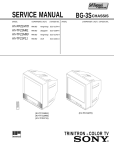
KV-1499M7J
RM-952
TABLE OF CONTENTS
Section
Title
Page
SELF DIAGNOSIS FUNCTION ................................ 4
Section
5-1.
5-2.
5-3
5-4.
(1)
(2)
(3)
5-5.
2. DISASSEMBLY
Rear Cover Removal ................................................
Chassis Assy Removal .............................................
F Bracket Removal ..................................................
Service Position .......................................................
Replacement of Parts ...............................................
2-5-1.
2-5-2.
2-6.
2-7.
2-8.
Replacement of Control Button .......................
Replacement of Light Guide ............................
Terminal Bracket Removal ......................................
Degauss Coil Removal .............................................
Picture Tube Removal ..............................................
18
18
18
18
19
19
19
19
19
20
Beam Landing ..........................................................
Convergence .............................................................
Focus Adjustment ....................................................
G2 (Screen) and White Balance Adjustments .........
6-1.
4-5.
Adjustments with Commander ................................
Adjustment Method .................................................
Picture Quality Adjustments ....................................
A Board Adjustment After IC003 (Memory)
Replacement .............................................................
Picture Distortion Adjustment .................................
35
38
40
41
43
47
54
59
Chassis ..................................................................... 62
7. ELECTRICAL PARTS LIST ...................................... 64
21
22
24
24
4. CIRCUIT ADJUSTMENT
4-1.
4-2.
4-3.
4-4.
Block Diagram .........................................................
Frame Schematic Diagram ......................................
Circuit Boards Location ..........................................
Schematic Diagrams and Printed Wiring Boards ...
Schematic Diagram of A (1/2) Board ......................
Schematic Diagram of A (2/2) Board ......................
Schematic Diagrams of C3 and F Boards ...............
Semiconductors ........................................................
6. EXPLODED VIEW
3. SET-UP ADJUSTMENTS
3-1.
3-2.
3-3.
3-4.
Page
5. DIAGRAMS
1. GENERAL ........................................................................ 8
2-1.
2-2.
2-3.
2-4.
2-5.
Title
25
26
31
31
32
–3–