
1
Order Number: MCUK980101C8
Service Manual
G600 Personal Cellular Telephone
Handheld Portable
EB-G600
Battery Packs
EB-BS600
EB-BM600
EB-BL600
Handsfree Car Mount Kit
EB-HF600Z
Easy Fit Car Kit
EB-HF601Z
Hands Free Car Kit
EB-HF600
Simple Car Kit
EB-KD600
DC Adaptor
EB-CD600
Dual Charger
EB-CR600
AC Adaptor
EB-CA600
Data Interface Cable
EB-PA600
SMS Interface Cable
EB-RS600
Issue 1
Revision 0
This Service Manual is copyright and issued on the strict understanding that it is not to be reproduced, copied, or
disclosed to any third party, either in whole or part, without the prior written consent of Matsushita Communication
Industrial UK Ltd.
Every care has been taken to ensure that the contents of this manual give an accurate representation of the
equipment. However, Matsushita Communication Industrial UK Ltd. accepts no responsibility for inaccuracies which
may occur and reserves the right to make changes to specification or design without prior notice.
The information contained in this manual and all rights in any designs disclosed therein, are and remain the
exclusive property of Matsushita Communication Industrial UK Ltd.
Other patents applying to material contained in this publication:
BULL CP8 PATENTS
Comments or correspondence concerning this manual should be addressed to:
Customer Support Department,
Matsushita Communication Industrial UK Ltd.,
Colthrop,
Thatcham,
Berkshire. RG19 4ZD.
ENGLAND
© 1998 Matsushita Communication Industrial UK Ltd.
Issue 1
Revision 0
ii
MCUK980101C8
Service Manual
TABLE OF CONTENTS
1
2
3
4
5
INTRODUCTION
1.1
Purpose of this Manual . . . . . . . . . . . . . . . . . . . . . . . . . . . . . . . . . . . . . . . . . . . . . 1-1
1.2
Structure of the Manual . . . . . . . . . . . . . . . . . . . . . . . . . . . . . . . . . . . . . . . . . . . . . 1-1
1.3
Servicing Responsibilities . . . . . . . . . . . . . . . . . . . . . . . . . . . . . . . . . . . . . . . . . . . . 1-1
GENERAL DESCRIPTION
2.1
General . . . . . . . . . . . . . . . . . . . . . . . . . . . . . . . . . . . . . . . . . . . . . . . . . . . . . 2-1
2.2
Handportable Main Kit . . . . . . . . . . . . . . . . . . . . . . . . . . . . . . . . . . . . . . . . . . . . . . 2-1
2.3
Handsfree Car Mount Kit . . . . . . . . . . . . . . . . . . . . . . . . . . . . . . . . . . . . . . . . . . . . 2-2
2.4
Easy Fit Car Kit . . . . . . . . . . . . . . . . . . . . . . . . . . . . . . . . . . . . . . . . . . . . . . . . . 2-3
2.5
Simple Car Kit . . . . . . . . . . . . . . . . . . . . . . . . . . . . . . . . . . . . . . . . . . . . . . . . . . 2-4
2.6
AC Adaptor . . . . . . . . . . . . . . . . . . . . . . . . . . . . . . . . . . . . . . . . . . . . . . . . . . . 2-4
2.7
SMS Interface Cable
2.8
DC Adaptor . . . . . . . . . . . . . . . . . . . . . . . . . . . . . . . . . . . . . . . . . . . . . . . . . . . 2-5
. . . . . . . . . . . . . . . . . . . . . . . . . . . . . . . . . . . . . . . . . . . . . . 2-5
2.9
Holder Kit . . . . . . . . . . . . . . . . . . . . . . . . . . . . . . . . . . . . . . . . . . . . . . . . . . . . 2-6
2.10
Dual Charger and Carry Case . . . . . . . . . . . . . . . . . . . . . . . . . . . . . . . . . . . . . . . . . . 2-6
2.11
Battery Packs . . . . . . . . . . . . . . . . . . . . . . . . . . . . . . . . . . . . . . . . . . . . . . . . . . 2-7
2.12
PC Card . . . . . . . . . . . . . . . . . . . . . . . . . . . . . . . . . . . . . . . . . . . . . . . . . . . . . 2-7
2.13
Documentation
2.14
Accessories . . . . . . . . . . . . . . . . . . . . . . . . . . . . . . . . . . . . . . . . . . . . . . . . . . . 2-8
. . . . . . . . . . . . . . . . . . . . . . . . . . . . . . . . . . . . . . . . . . . . . . . . . 2-8
OPERATING INSTRUCTIONS
3.1
General . . . . . . . . . . . . . . . . . . . . . . . . . . . . . . . . . . . . . . . . . . . . . . . . . . . . . 3-1
3.2
LCD Display . . . . . . . . . . . . . . . . . . . . . . . . . . . . . . . . . . . . . . . . . . . . . . . . . . . 3-1
3.3
Location of Controls . . . . . . . . . . . . . . . . . . . . . . . . . . . . . . . . . . . . . . . . . . . . . . . 3-2
3.4
Concept of Operation . . . . . . . . . . . . . . . . . . . . . . . . . . . . . . . . . . . . . . . . . . . . . . 3-3
3.5
Alpha Entry . . . . . . . . . . . . . . . . . . . . . . . . . . . . . . . . . . . . . . . . . . . . . . . . . . . 3-3
3.6
Incoming Calling Line Identification (CLI) . . . . . . . . . . . . . . . . . . . . . . . . . . . . . . . . . . . . 3-4
3.7
Features Menu Structure . . . . . . . . . . . . . . . . . . . . . . . . . . . . . . . . . . . . . . . . . . . . 3-4
3.8
Public Man Machine Interface (MMI) . . . . . . . . . . . . . . . . . . . . . . . . . . . . . . . . . . . . . . 3-5
3.9
Troubleshooting . . . . . . . . . . . . . . . . . . . . . . . . . . . . . . . . . . . . . . . . . . . . . . . . . 3-8
3.10
Important Error Messages . . . . . . . . . . . . . . . . . . . . . . . . . . . . . . . . . . . . . . . . . . . . 3-9
3.11
Security Codes . . . . . . . . . . . . . . . . . . . . . . . . . . . . . . . . . . . . . . . . . . . . . . . . . 3-10
3.12
GSM Services Supported by PC Card . . . . . . . . . . . . . . . . . . . . . . . . . . . . . . . . . . . . . 3-10
3.13
GSM Network Codes and Names . . . . . . . . . . . . . . . . . . . . . . . . . . . . . . . . . . . . . . . 3-11
3.14
Glossary of Terms . . . . . . . . . . . . . . . . . . . . . . . . . . . . . . . . . . . . . . . . . . . . . . . 3-15
INSTALLATION GUIDE
4.1
General . . . . . . . . . . . . . . . . . . . . . . . . . . . . . . . . . . . . . . . . . . . . . . . . . . . . . 4-1
4.2
Handsfree Car Mount Kit . . . . . . . . . . . . . . . . . . . . . . . . . . . . . . . . . . . . . . . . . . . . 4-1
4.3
DC Adaptor . . . . . . . . . . . . . . . . . . . . . . . . . . . . . . . . . . . . . . . . . . . . . . . . . . . 4-6
4.4
Simple Car Kit . . . . . . . . . . . . . . . . . . . . . . . . . . . . . . . . . . . . . . . . . . . . . . . . . . 4-6
DISASSEMBLY/REASSEMBLY INSTRUCTIONS
5.1
General . . . . . . . . . . . . . . . . . . . . . . . . . . . . . . . . . . . . . . . . . . . . . . . . . . . . . 5-1
5.2
Handportable Unit . . . . . . . . . . . . . . . . . . . . . . . . . . . . . . . . . . . . . . . . . . . . . . . . 5-2
5.3
Dual Charger
5.4
Handsfree Unit
5.5
Easy Fit Unit . . . . . . . . . . . . . . . . . . . . . . . . . . . . . . . . . . . . . . . . . . . . . . . . . . 5-11
MCUK980101C8
Service Manual
. . . . . . . . . . . . . . . . . . . . . . . . . . . . . . . . . . . . . . . . . . . . . . . . . . 5-6
. . . . . . . . . . . . . . . . . . . . . . . . . . . . . . . . . . . . . . . . . . . . . . . . . 5-8
iii
Issue 1
Revision 0
6
7
8
9
10
TECHNICAL SPECIFICATIONS
6.1
General . . . . . . . . . . . . . . . . . . . . . . . . . . . . . . . . . . . . . . . . . . . . . . . . . . . . . 6-1
6.2
Handportable Unit . . . . . . . . . . . . . . . . . . . . . . . . . . . . . . . . . . . . . . . . . . . . . . . . 6-1
6.3
Handsfree Unit
6.4
Dual Charger
6.5
AC Adaptor . . . . . . . . . . . . . . . . . . . . . . . . . . . . . . . . . . . . . . . . . . . . . . . . . . . 6-6
6.6
DC Adaptor . . . . . . . . . . . . . . . . . . . . . . . . . . . . . . . . . . . . . . . . . . . . . . . . . . . 6-6
6.7
Battery Packs . . . . . . . . . . . . . . . . . . . . . . . . . . . . . . . . . . . . . . . . . . . . . . . . . . 6-7
6.8
Features of Lithium-Ion (Li-Ion) batteries . . . . . . . . . . . . . . . . . . . . . . . . . . . . . . . . . . . . 6-8
. . . . . . . . . . . . . . . . . . . . . . . . . . . . . . . . . . . . . . . . . . . . . . . . . 6-5
. . . . . . . . . . . . . . . . . . . . . . . . . . . . . . . . . . . . . . . . . . . . . . . . . . 6-5
TEST AND MEASUREMENT
7.1
Introduction . . . . . . . . . . . . . . . . . . . . . . . . . . . . . . . . . . . . . . . . . . . . . . . . . . . 7-1
7.2
External Testing . . . . . . . . . . . . . . . . . . . . . . . . . . . . . . . . . . . . . . . . . . . . . . . . . 7-1
7.3
Complete Unit Test Setup . . . . . . . . . . . . . . . . . . . . . . . . . . . . . . . . . . . . . . . . . . . . 7-3
7.4
Channel Box Test Commands
7.5
Adjustment Mode . . . . . . . . . . . . . . . . . . . . . . . . . . . . . . . . . . . . . . . . . . . . . . . . 7-9
7.6
Lock Code . . . . . . . . . . . . . . . . . . . . . . . . . . . . . . . . . . . . . . . . . . . . . . . . . . . 7-21
7.7
SIM Personalisation . . . . . . . . . . . . . . . . . . . . . . . . . . . . . . . . . . . . . . . . . . . . . . 7-22
. . . . . . . . . . . . . . . . . . . . . . . . . . . . . . . . . . . . . . . . . 7-7
CIRCUIT DIAGRAMS
8.1
Handheld Unit . . . . . . . . . . . . . . . . . . . . . . . . . . . . . . . . . . . . . . . . . . . . . . . . . . 8-1
8.2
Handsfree . . . . . . . . . . . . . . . . . . . . . . . . . . . . . . . . . . . . . . . . . . . . . . . . . . . . 8-5
8.3
Easy-Fit Handsfree . . . . . . . . . . . . . . . . . . . . . . . . . . . . . . . . . . . . . . . . . . . . . . . 8-6
PCB LAYOUT DIAGRAMS
9.1
Handheld Unit . . . . . . . . . . . . . . . . . . . . . . . . . . . . . . . . . . . . . . . . . . . . . . . . . . 9-1
9.2
Handsfree . . . . . . . . . . . . . . . . . . . . . . . . . . . . . . . . . . . . . . . . . . . . . . . . . . . . 9-3
9.3
Easy-Fit Handsfree . . . . . . . . . . . . . . . . . . . . . . . . . . . . . . . . . . . . . . . . . . . . . . . 9-4
PARTS LIST
10.1
Handheld Unit . . . . . . . . . . . . . . . . . . . . . . . . . . . . . . . . . . . . . . . . . . . . . . . . . 10-1
10.2
Handsfree Unit . . . . . . . . . . . . . . . . . . . . . . . . . . . . . . . . . . . . . . . . . . . . . . . . . 10-2
10.3
Handheld Replacement Parts List . . . . . . . . . . . . . . . . . . . . . . . . . . . . . . . . . . . . . . . 10-3
10.4
Handsfree Replacement Parts List . . . . . . . . . . . . . . . . . . . . . . . . . . . . . . . . . . . . . . 10-15
10.5
Printed Material . . . . . . . . . . . . . . . . . . . . . . . . . . . . . . . . . . . . . . . . . . . . . . . . 10-22
10.6
Dual Charger . . . . . . . . . . . . . . . . . . . . . . . . . . . . . . . . . . . . . . . . . . . . . . . . . 10-22
10.7
DC Adaptor . . . . . . . . . . . . . . . . . . . . . . . . . . . . . . . . . . . . . . . . . . . . . . . . . . 10-22
10.8
PC Card. . . . . . . . . . . . . . . . . . . . . . . . . . . . . . . . . . . . . . . . . . . . . . . . . . . . 10-22
Issue 1
Revision 0
iv
MCUK980101C8
Service Manual
WARNINGS AND CAUTIONS
WARNING
The equipment described in this manual contains polarized capacitors utilising liquid electrolyte. These devices
are entirely safe provided that neither a short-circuit nor a reverse polarity connection is made across the
capacitor terminals. FAILURE TO OBSERVE THIS WARNING COULD RESULT IN DAMAGE TO THE
EQUIPMENT OR, AT WORST, POSSIBLE INJURY TO PERSONNEL RESULTING FROM ELECTRIC SHOCK
OR THE AFFECTED CAPACITOR EXPLODING. EXTREME CARE MUST BE EXERCISED AT ALL TIMES
WHEN HANDLING THESE DEVICES.
Caution
The equipment described in this manual contains electrostatic sensitive devices (ESDs). Damage can occur to
these devices if the appropriate handling procedure is not adhered to.
ESD Handling precautions:
A working area where ESDs may be safely handled without undue risk of damage from electrostatic discharge,
must be available. The area must be equipped as follows:
Working Surfaces - All working surfaces must have a dissipative bench mat, SAFE for use with live equipment,
connected via a 1M2 resistor (usually built into the lead) to a common ground point.
Wrist Strap - A quick release skin contact device with a flexible cord, which has a built in safety resistor of between
5k2 and 1M2 shall be used. The flexible cord must be attached to a dissipative earth point.
Containers - All containers and storage must be of the conductive type.
Batteries
This equipment may contain an internal battery in addition to the external battery packs. These batteries are
recyclable and should be disposed of in accordance with local legislation. They must not be incinerated, or
disposed of as ordinary rubbish.
MCUK980101C8
Service Manual
v
Issue 1
Revision 0
This page is intentionally blank
Issue 1
Revision 0
vi
MCUK980101C8
Service Manual
INTRODUCTION
1
1.1
INTRODUCTION
Purpose of this Manual
This Service Manual contains the information and procedures required for installing, operating and servicing the
Panasonic GSM Personal Cellular Mobile Telephone system operating on the GSM Digital Cellular Network.
1.2
Structure of the Manual
The manual is structured to provide service engineering personnel with the following information and procedures:
1. General and technical information - provides a basic understanding of the equipment, kits and options, together
with detailed information for each of the major component parts.
2. Installation and operating information - provides instructions for unpacking, installing and operating the
equipment.
3. Servicing information - provides complete instructions for the testing, disassembly, repair and reassembly of
each major component part. Step-by-step troubleshooting information is given to enable the isolation and
identification of a malfunction, and thus determine what corrective action should be taken. The test information
enables verification of the integrity of the equipment after any remedial action has been carried out.
4. Illustrated parts list - provided to enable the identification of all equipment components, for the ordering of
spare/replacement parts.
1.3
Servicing Responsibilities
The procedures described in this manual must be performed by qualified service engineering personnel, at an
authorised service centre.
The service engineering personnel are responsible for fault diagnosis and repair of all equipment described in this
manual.
MCUK980101C8
Service Manual
Section 1
1-1
Issue 1
Revision 0
INTRODUCTION
This page is intentionally blank
Issue 1
Revision 0
Section 1
1-2
MCUK980101C8
Service Manual
GENERAL DESCRIPTION
2
2.1
GENERAL DESCRIPTION
General
This section provides a general description and kit composition details for the GSM Handportable Telephone
system and optional kits.
The GSM handportable may be configured as:
1. Handportable unit.
2. Vehicle-powered (DC adaptor) handportable unit.
3. Handsfree vehicle-mounted unit.
4. PC fax: send and receive (via PCMCIA Interface card).
2.2
Handportable Main Kit
The handportable main kit provides a standalone class 4 GSM telephone. The plug-in SIM contains the subscriber
and network information necessary to operate the phone on a GSM network.
Figure 1: Handportable Main Unit Kit
IDENTIFICATION NUMBER
1
2
3
—
MCUK980101C8
Service Manual
600-0201
DESCRIPTION
Main unit
Battery
Adaptor
Documentation
Section 2
2-1
PART NUMBER
EB-G600
EB-BS600
EB-CA600
See Section 2.13
Issue 1
Revision 0
GENERAL DESCRIPTION
2.3
Handsfree Car Mount Kit
The Handsfree Car Mount Kit enables the handportable to be mounted in a vehicle, and to operate in handsfree
mode.
The Handsfree Unit contains a speaker, with separate volume control. Speech is via a microphone mounted on the
dashboard or the sun visor.
The telephone can be operated in handheld mode by removing it from the Holder. This will use the external
antenna and power from the Handsfree Unit.
The handsfree unit also provides external power for the handheld internal charger.
Figure 2: Handsfree Car Mount Kit
IDENTIFICATION NUMBER
1
2
3
4
5
6
Issue 1
Revision 0
600-0202
DESCRIPTION
Handsfree unit
Holder
Handsfree microphone
Adjustable angle bracket
Adjustable angle bracket
Power supply cable
Section 2
2-2
PART NUMBER
EB-HF600
EB-KA600
EBM1177
EBN0001
EBN0002
EBW70090
MCUK980101C8
Service Manual
GENERAL DESCRIPTION
2.4
Easy Fit Car Kit
The Easy Fit Car Mount Kit is very similar to the Handsfree Car Mount Kit. The main difference with the Easy Fit
Car Mount kit is the addition of a cigar lighter adaptor for the supply of power. The cigar lighter adaptor makes
installation of the kit very simple.
The Handsfree Unit contains a speaker, with separate volume control. Speech is via a microphone mounted on the
dashboard or the sun visor.
Due to the length of cable from the Handsfree Unit to the telephone the telephone can only be used in handsfree
mode.
The Handsfree Unit also provides external power for the handheld internal charger.
Figure 4: Easy Fit Car Mount Kit
IDENTIFICATION NUMBER
1
2
3
4
5
MCUK980101C8
Service Manual
600-0203
DESCRIPTION
Handsfree unit
Holder
Handsfree microphone
Adjustable angle bracket
Car lighter adaptor
Section 2
2-3
PART NUMBER
EB-HF601
EB-KA600
EBM1177
EBN0001
WC70187A
Issue 1
Revision 0
GENERAL DESCRIPTION
2.5
Simple Car Kit
The Simple Car Kit enables the handportable unit to be powered from a vehicle battery, provided that the vehicle
has a cigar lighter socket, and also has an external antenna connector for better signal quality when in a vehicle.
One end of the DC adaptor plugs into the handportable with the telephone battery connected. The other end of the
adaptor is pushed into the cigar lighter socket. The external antenna connector is an FME type.
Figure 5: Simple Car Kit
2.6
600-0208
IDENTIFICATION NUMBER
DESCRIPTION
1
Simple Car Kit
PART NUMBER
EB-KD600
AC Adaptor
The AC Adaptor kit is supplied with UK or European input plug type; other country specific types are available. The
adaptor enables the handportable unit to be powered from a 230/110/100 VAC supply.
One end of the AC adaptor plugs into the handportable with the telephone battery connected. The other end of the
adaptor is pushed into the electrical supply socket.
1
Figure 2: AC Adaptor
IDENTIFICATION NUMBER
1
Issue 1
Revision 0
600-0212
DESCRIPTION
AC Adaptor
Section 2
2-4
PART NUMBER
EB-CA600
MCUK980101C8
Service Manual
GENERAL DESCRIPTION
2.7
SMS Interface Cable
The SMS Interface Cable enables Short Text Messages (SMS) and Phonebook data to be edited, stored and
created.
One end of the SMS Interface Cable is connected to the standalone class 4 GSM telephone and the other end of
the SMS Interface Cable is connected to the RS232 serial port on an IBM compatible PC.
1
Figure 3: SMS Interface Cable
2.8
600-0213
IDENTIFICATION NUMBER
DESCRIPTION
1
SMS I/F Cable
PART NUMBER
EB-RS600
DC Adaptor
The DC Adaptor kit enables the handportable unit to be powered from a vehicle battery, provided that the vehicle
has a cigar lighter socket.
One end of the DC adaptor plugs into the handportable with the telephone battery connected. The other end of the
adaptor is pushed into the cigar lighter socket.
Figure 6: DC Adaptor
IDENTIFICATION NUMBER
1
MCUK980101C8
Service Manual
600-0209
DESCRIPTION
DC Adaptor unit
Section 2
2-5
PART NUMBER
EB-CD600
Issue 1
Revision 0
GENERAL DESCRIPTION
2.9
Holder Kit
The holder kit allows convenient mounting of the telephone in a vehicle. In conjunction with the DC adaptor this can
make a simple car mount kit. The adjustable angle bracket and telephone holder are attached to a convenient fixing
point in the vehicle.
1
2
Figure 7: Holder Kit
600-0204
IDENTIFICATION NUMBER
1
2
DESCRIPTION
PART NUMBER
Holder
Adjustable Angle Bracket
EB-KA600
EBN0002
2.10 Dual Charger and Carry Case
The dual charger has two charging slots, enabling the telephone battery to be charged individually or as a part of
the whole telephone assembly.
2
1
Figure 8: Dual Charger and Carry Case
Issue 1
Revision 0
500-0205
IDENTIFICATION NUMBER
DESCRIPTION
1
2
Dual charger
Carry case
Section 2
2-6
PART NUMBER
EB-CR600
EB-YK400
MCUK980101C8
Service Manual
GENERAL DESCRIPTION
2.11 Battery Packs
There is a choice of three battery packs available. The Battery Pack (S) is 400mAh (Li-Ion); the Battery Pack (M) is
650mAh (Ni-MH and the Battery Pack (L) is 1200mAh (Li-Ion).
2
1
3
Figure 9: Battery Packs
IDENTIFICATION NUMBER
1
2
3
600-0211
DESCRIPTION
Battery Pack (S)
Battery Pack (M)
Battery Pack (L)
PART NUMBER
EB-BS600
EB-BM600
EB-BL600
2.12 PC Card
The PC Card interface is used with the handportable and a laptop personal computer to provide a PC fax and
modem facility.
Figure 10: PC Card
600-0207
IDENTIFICATION NUMBER
DESCRIPTION
1
PC Card
Handsfree unit
– connection
Telephone
– connection
2
3
MCUK980101C8
Service Manual
Section 2
2-7
PART NUMBER
EB-PA600
—
—
Issue 1
Revision 0
GENERAL DESCRIPTION
2.13 Documentation
The following documentation packs are available and contain Operating Instructions, Quick Start information and
warranty information. Some markets may require additional documentation, e.g. a specific warranty, that is not
listed.
DOCUMENTATION PACKS
Austria
Belgium
Czech Republic
Denmark
Finland
France
Germany
Greece
Italy
Kuwait
Lebanon
Netherlands
Poland
Portugal
Russia
Slovakia
Spain
Sweden
Switzerland
Turkey
United Kingdom
Yugoslav Republic
G600DOCAS
G600DOCBE
G600DOCCZ
G600DOCDE
G600DOCFI
G600DOCFR
G600DOCGE
G600DOCGR
G600DOCIT
G600DOCKU
G600DOCLE
G600DOCNL
G600DOCPL
G600DOCPO
G600DOCRU
G600DOCSK
G600DOCES
G600DOCSW
G600DOCCH
G600DOCTU
G600DOCUK
G600DOCYU
2.14 Accessories
In addition to the kit contents listed in this section, all kits also contain user documentation. Some markets may
require additional documentation, e.g. a specific warranty, that is not listed.
OPTIONAL ACCESSORIES
Handsfree Car Mount Kit
Car Mount Kit
Easy Fit Car Mount Kit
Simple Car Kit
DC Adaptor
Holder Kit
Dual Charger
Carry Case
Battery Pack (S)
Battery Pack (M)
Battery Pack (L)
AC Adaptor
SMS Interface Cable
Data Interface Card
Issue 1
Revision 0
EB-HF600
EBHF600Z
EB-HF601Z
EB-KD600
EB-CD600
EB-KA600
EB-CR600
EB-YK600
EB-BS600
EB-BM600
EB-BL600
EB-CA600
EB-RS600
EB-PA600
Section 2
2-8
MCUK980101C8
Service Manual
OPERATING INSTRUCTIONS
3
OPERATING INSTRUCTIONS
3.1
General
This section provides a brief guide to the operation and facilities available on the G600 handportable unit. Refer to
the Operating Instructions for full operational information.
3.2
LCD Display
The G600 handportable unit has a graphical chip on glass liquid crystal display in conjunction with the following
icons:
Option
Area
Menu
Number
Figure 1: LCD display
600-0301
T
Indicates received signal strength: T strong signal area;\ weak signal area.
S
Indicates that it is possible to make an emergency call.
Menu
Number
The number of the feature pointed to by the pointer. To access a feature enter the menu number on
the keypad.
H
Displays the battery charge level: H Battery is at full charge; K Battery
requires recharging;
G The battery icon flashes during charging. During car mount use, when the battery is fully
charged, the battery icon will not light.
Displays a small icon related to the current status of the telephone:
Y telephone is roaming on a none home network;
t using the “Call Divert” feature or the telephone has Call Divert set; u Call Divert profile 1 is set;
] shows that the vibration alert is switched on;
[ shows that telephone is in silent mode - no tones;
Menu
Icon
N indicates there are unread Short Text Messages (SMS.). Lit when SMS area is full;
O the telephone is locked;
U shows that normal character have been entered in Alpha Entry;
V shows that Greek character have been entered in Alpha Entry;
W shows that extended character have been entered in Alpha Entry;
X shows that numbers have been entered in Alpha Entry.
p
Indicates that the navigation key (g) can be pressed. Each arrow will light individually to indicate
which direction is valid.
Option
Area
Pressing the select key (B) will select the option displayed in the option area of the display.
Following some operations the display will automatically clear after three seconds or after pressing any key except
E.
MCUK980101C8
Service Manual
Section 3
3-1
Issue 1
Revision 0
OPERATING INSTRUCTIONS
3.3
Location of Controls
Incoming/Charge indicator:
Green – incoming call.
Red – charging battery pack.
External connector:
Used to connect to external accessories or charging equipment.
Figure 2: Location of controls for G600
600-0302
:
Memo Key. Record a conversation for approximately 40 seconds during a call.
g
Navigation Key. Scrolls through options or features menu and increases or decreases volume.
B
Select Key. Selects option shown in the Option Area of the display.
A
Phonebook Key. Browses through the Phonebook or stores a number in the Phonebook. Changes the
type of characters entered during Alpha Entry.
D
Send Key. Makes a call.
C
Clear Key. Clears the last digit entered, clears all digits when pressed and held or returns to the previous
display.
E
End Key. Ends a call or switches the telephone on/off when pressed and held.
Digit keys 0 to 9, and where appropriate the 0 key will enter the international access code “+”, wild
numbers or pauses when pressed and held. The # key, when pressed and held, enables or disables the
vibrator.
Issue 1
Revision 0
Section 3
3-2
MCUK980101C8
Service Manual
OPERATING INSTRUCTIONS
3.4
Concept of Operation
There is a close relationship between the Select Key, Navigation Key and display.
Figure 3: Concept of Operation
600-0303
Pressing up and down (e) will move the pointer up and down and scroll through more information in the main area
of the display.
Pressing left and right (f) will scroll through options in the option area of the display. To choose the option press
the Select Key (B).
3.5
Alpha Entry
Alpha Entry is used to enter alphanumeric characters into Phonebook, Short Messages and the Greeting Message.
Character/Operation
Key
U
V
W
X
1
“@–,.;:!¡?¿()‘&%+–/<>=£$¥¤§
2
ABCabc
ΑΒΓ
AÄÅÆBCÇaàbc
2
3
DEFdef
∆ΕΖ
DEÉFdeèéf
3
4
GHIghi
ΗΘΙ
GHIghiì
4
5
JKLjkl
ΚΛΜ
JKLjkl
5
6
MNOmno
ΝΞΟ
MNÑOÖømnñoòö
6
7
PQRSpqrs
ΠΡΣ
PQRSpqrsß
7
8
TUVtuv
ΤΥΦ
TUÜVtuùüv
8
9
WXYZwxyz
ΞΨΩ
WXYZwxyz
9
C
Deletes the character above the cursor, deletes the character to the left when at the end of the line or
clears the entire entry when pressed and held.
1
Each time a key is pressed it will display the next character. When another key is pressed or no key is pressed for
a short time the cursor will move to the next position.
To cycle between Greek characters (V), extended characters (W), numerals (X) and normal characters (U)
press A.
3.5.1 Editing Alpha Entry
Pressing e will move you up or down one line. Pressing f will move you left or right one character. When the
cursor is moved over a character and another key pressed this will insert the new character.
Pressing C will delete the character to the left of the cursor.
MCUK980101C8
Service Manual
Section 3
3-3
Issue 1
Revision 0
OPERATING INSTRUCTIONS
3.6
Incoming Calling Line Identification (CLI)
When a call is received the last 6 digits of the CLI information is matched with the phonebook. Therefore an
incoming call could match to the wrong phonebook entry.
3.7
Features Menu Structure
Figure 4: Feature Menu
Issue 1
Revision 0
600-0304
Section 3
3-4
MCUK980101C8
Service Manual
OPERATING INSTRUCTIONS
3.8
Public Man Machine Interface (MMI)
It is possible to operate all GSM telephones in the same way using the Public MMI. The following operations will
work with all GSM telephones. However, this information is restricted to those operations that are supported by
G600.
The * and # in the following procedures should be replaced by * and #, respectively. Also <SND> and <END>
should be replaced with D and E keys.
3.8.1 Reading Phonebook Memory Location
# <MEMORY LOCATION>
Leading zeros can be left out of the location number, e.g. 007 can be 7.
3.8.2 Presentation of IMEI
*#06#
3.8.3 Security
Change PIN
* * 0 4 * <OLD PIN> * <NEW PIN> * <NEW PIN> #
Change PIN2
* * 0 4 2 * <OLD PIN2> * <NEW PIN2> * <NEW PIN2> #
Unblock PIN
* * 0 5 * <PIN UNBLOCKING KEY> * <NEW PIN> * <NEW PIN> #
Unblock PIN2
* * 0 5 2 * <PIN2 UNBLOCKING KEY> * <NEW PIN2> * <NEW PIN2> #
3.8.4 Call Hold
Place a call on hold
2 <SND>
Recall a held call
2 <SND>
Make a second call
<TELEPHONE NUMBER> <SND>
Swap between two held calls
2 <SND>
End held call
O <SND>
End active call
1 <SND>
Reject incoming call
0 <SND>
MCUK980101C8
Service Manual
Section 3
3-5
Issue 1
Revision 0
OPERATING INSTRUCTIONS
3.8.5 Call Waiting
Enable Call Waiting
* 4 3 * # <SND>
Disable Call Waiting
# 4 3 * # <SND>
Call Waiting Status
* # 4 3 * # <SND>
3.8.6 Calling Line Identification
Calling Line Identification Feature
Service Code
Calling Line Identification Presentation (CLIP)
30
Calling Line Identification Restriction (CLIR)
31
Connected Line Presentation (CLOP)
76
Connected Line Restriction (CLOR)
77
Enable
* <SERVICE CODE> * # <SND>
Disable
# <SERVICE CODE> * # <SND>
Temporary suppress identification
# 3 1 # <TELEPHONE NUMBER> <SND>
Temporary display identification * 3 1 # <TELEPHONE NUMBER> <SND>
3.8.7 Call Divert
Call Divert Type
Service Code
Divert all calls
21
Divert calls if busy
67
Divert calls if no reply
61
Divert if not reachable
62
Set (except “No Reply” Call Bar
* * <SERVICE CODE> * <FORWARD TELEPHONE NUMBER> * <TELECOMMUNICATION SERVICE> # <SND>
Set “No Reply” Call Bar
* * <SERVICE CODE> * <FORWARD TELEPHONE NUMBER> * <TELECOMMUNICATION SERVICE> *
<TIME TO RING (seconds) # <SND>
Clear
# # <SERVICE CODE> * <TELECOMMUNICATION SERVICE> * # <SND>
Status
* # <SERVICE CODE> * <TELECOMMUNICATION SERVICE> * # <SND>
Clear all Call Diverts
##002#
Issue 1
Revision 0
Section 3
3-6
MCUK980101C8
Service Manual
OPERATING INSTRUCTIONS
3.8.8 Call Bar
Call Bar Type
Service Code
All outgoing calls
33
Outgoing international calls
331
Outgoing international calls except those to your PLMN country
332
All incoming calls
35
Incoming international calls when roaming
351
Set
* <PASSWORD> * <TELECOMMUNICATION SERVICE> # <SND>
Clear
# <PASSWORD> * <TELECOMMUNICATION SERVICE> # <SND>
Status
* # <TELECOMMUNICATION SERVICE> # <SND>
Clear all Call Bar Types
# 3 3 0 * <PASSWORD> # <SND>
Change Call Bar Password
* * 0 3 * * <OLD PASSWORD> * <NEW PASSWORD> * <NEW PASSWORD> # <SND>
3.8.9 Telecommunication Services Used for Public MMI
Teleservice
Service
MMI Service Code
All teleservices
10
Telephony
11
All data teleservices
12
Facsimile services
13
Short Message Services (SMS)
16
All teleservices except SMS
19
Voice group services
17
Bearer Service
Service
MMI Service Code
All bearer services
20
All asynchronous services
21
All synchronous services
22
All data synchronous services
24
All data asynchronous services
25
All dedicated packet access
26
All dedicated PAD access
27
MCUK980101C8
Service Manual
Section 3
3-7
Issue 1
Revision 0
OPERATING INSTRUCTIONS
3.9
Troubleshooting
The user is given the following information and advised to contact the dealer if the problems persist:
Problem
Telephone will not
switch on
Cause
Extremely short
battery life for a new
battery pack
The network you are using and the
condition of the battery pack can
affect battery life
Short battery life for
an old battery pack
The battery pack was worn out
Short battery life for
Ni-MH battery pack
The battery level
indicator H does
not light when
charging
Calls cannot be
made
Calls cannot be
made from Fixed
Dial Store
Calls cannot be
received
Emergency calls
cannot be made
Telephone numbers
cannot be recalled
Issue 1
Revision 0
Remedy
Check that the battery pack is fully charged and
correctly connected to the telephone
Avoid areas of poor reception. Ensure batteries
are fully charged. Additionally, for NiMH batteries,
ensure batteries are also discharged fully before
recharging.
Replace with a new one
To maintain maximum performance always use
until the Low Battery Warning and then fully
recharge the battery pack
The life of the battery pack is affected
by improper charging, this is inherent To revive the Battery Pack use the telephone until
the Low Battery Warning and then fully recharge
in all Ni-MH batteries
three times. However, if the battery life still is short,
the battery pack has eventually worn out. Replace
with a new one
If a battery is deeply discharged it will
take a short time before there is
Leave to charge for several minutes in
sufficient power in the telephone to
temperatures between +5°C and +35°C
light the battery level indicator H
Unlock the telephone (Menu: Security: Phone
The telephone is locked
Lock)
Disable the outgoing call barring (Menu: Security:
Outgoing calls are barred
Call Bar)
The telephone is not registered to a
Move to a coverage area and operate your
network
telephone after it has registered with a network
Check your SIM supports Fixed Dial
Check if the Fixed Dial is switched on (Menu:
Security: Fixed Dial)
Check the telephone number is stored in the Fixed
Dial
The telephone is not switched on
Switch the telephone on
Disable the incoming call barring (Menu: Security:
Incoming calls are barred
Call Bar)
The telephone is not registered to a
Move to a coverage area and operate your
network
telephone after it has registered with a network
You are not in a GSM coverage area
The telephone is locked
Fixed Dial is switched on
Section 3
3-8
Check that the antenna symbol S is displayed.
Move to a coverage area and operate your
telephone when the antenna symbol is displayed
Unlock the telephone (Menu: Security: Phone
Lock)
Switch off Fixed Dial (Menu: Security: Fixed Dial)
MCUK980101C8
Service Manual
OPERATING INSTRUCTIONS
3.10 Important Error Messages
The following table is a list of error messages that may occur during use of the telephone, with a description and
suggested course of action:
Area not
Allowed
Roaming in the selected area is not allowed
Network
not Allowed
Roaming with the selected network is not allowed
Security
Failure
The network has detected authentication failure because your SIM is not registered with that
network. Contact your Service Provider
SIM
Blocked
The SIM is blocked because the wrong PUK has been entered ten times. Contact your Service
Provider
SIM Error
The telephone has detected a problem with the SIM. Switch the telephone off and then back on. If
the message does not disappear contact your Service Provider
Message
Rejected
Store Full
A message has been received but the message store is full. To receive messages, delete some of
the currently stored messages or set messages to automatically clear (Menu: Messages:
Parameters: Auto Delete)
PIN2
Invalidated
The PIN2 is blocked permanently because the wrong PUK2 has been entered 10 times. Services
controlled by PIN2 cannot be used. Contact your Service Provider
Warning
Store Full
Continue?
The message area is full. Your messages cannot be stored until some of the currently stored
messages are deleted
Auto Redial
List Full
Redial list of unsuccessfully dialled numbers is full. Switch the telephone off and then on again
MCUK980101C8
Service Manual
Section 3
3-9
Issue 1
Revision 0
OPERATING INSTRUCTIONS
3.11 Security Codes
NUMBER OF
DIGITS
CODE TYPE
DESCRIPTION
Personal Identification
Number (PIN)
4 to 8
Controls SIM security. Supplied by the service provider.
PIN 2
4 to 8
Controls memory security. Supplied by the service provider.
PIN/PIN 2 Unblocking Key
(PUK/PUK 2)
8
Used to unblock PIN and PIN 2. A PIN or PIN 2 will become
blocked if the wrong PIN or PIN 2 is entered three times.
When the blocked PIN or PIN 2 is unblocked, a new PIN or
PIN 2 must be entered. If the wrong PUK or PUK 2 is entered
10 times, your SIM will be unusable.
Supplied by the service provider.
Password
4
Controls the call bar function. If the wrong password is
entered three times, this service will be revoked. Supplied by
the service provider.
Lock Code
4
Controls telephone security.
Factory set to “0000”.
3.12 GSM Services Supported by PC Card
Bearer
Service
Number
Bearer Service Rate
Access
Structure
Access Rate
Information
Transfer
Error
Correction
Options
21
Asynchronous 300 bps
Asynch
300 bps
UDI or
modem
T or NT
22
Asynchronous 1.2 kbps
Asynch
1.2 kbps
UDI or
modem
T or NT
23
Asynchronous 1200/75 bps
Asynch
1200/75 bps
UDI or
modem
T or NT
24
Asynchronous 2.4 kbps
Asynch
2.4 kbps
UDI or
modem
T or NT
25
Asynchronous 4.8 kbps
Asynch
4.8 kbps
UDI or
modem
T or NT
26
Asynchronous 9.6 kbps
Asynch
9.6 kbps
UDI or
modem
T or NT
41
Dedicated PAD Access 300
bps
Asynch
300 bps
UDI
T or NT
42
Dedicated PAD Access 1.2
kbps
Asynch
1.2 kbps
UDI
T or NT
44
Dedicated PAD Access 2.4
kbps
Asynch
2.4 kbps
UDI
T or NT
45
Dedicated PAD Access 4.8
kbps
Asynch
4.8 kbps
UDI
T or NT
46
Dedicated PAD Access 9.6
kbps
Asynch
9.6 kbps
UDI
T or NT
Issue 1
Revision 0
Section 3
3 - 10
MCUK980101C8
Service Manual
OPERATING INSTRUCTIONS
3.13 GSM Network Codes and Names
Country
Access
Code
Albania
+355
AMC
276
01
Andorra
+376
STA -Mobiland
213
03
TELECOM Australia
505
01
OPTUS Communications Pty Ltd.
505
02
Vodafone PTY
505
03
Mobilkom Austria
232
01
max.mobil
232
03
Azercell
400
01
Cronet
218
01
PTT Bosnia
218
19
Belgacom Mobile
206
01
Mobistar
206
10
Australia
+61
Network Operator
Network
Code
Austria
+43
Azerbaijan
+994
Bosnia & Herzegowina
+387
Belgium
+32
Bulgaria
+359
MOBILTEL AD
284
01
Bahrein
+973
BAHREIN Telecommunications Co.
426
01
Brunei Darussalam
+673
DSTCom
528
11
Jabatan Telekom
528
01
Canada
+1
Microcell
302
37
China
+86
Guangdong MCC
460
00
China United Telecommuni-cations Corporation
460
01
Cameroon
+237
PTT Cameroon Cellnet
624
01
Cyprus
+357
Cyprus Telecommunication Authority
280
01
Czech Republic
+42
Eurotel Praha
230
02
Radio Mobil
230
01
Germany
+49
DeTeMobil GmbH
262
01
Mannesmann Mobilfunk
262
02
Denmark
+45
TELE Danmark Mobile
238
01
Dansk Mobil Telefon DMT
238
02
Estonia
+372
Eesti Mobiiltelefon
248
01
RADIOLINJA EESTI AS
248
02
Egypt
+20
Arento
602
01
Ethiopia
+251
ETA
636
01
France Telecom
208
01
SFR
208
10
Bouygues Telekom
208
20
SRR
647
10
TIKIPHONE
547
20
Telecom Finland
244
91
Finnet
244
09
OY Radiolinja AB
244
05
Vodafone
542
01
Geocell
282
01
Magticom
282
02
France
Finland
+33
+358
Fiji
+679
Georgia
+995
MCUK980101C8
Service Manual
Section 3
3 - 11
Issue 1
Revision 0
OPERATING INSTRUCTIONS
Ghana
+233
ScanCom
620
01
Gibralta
+350
GIBTEL
266
01
Greece
+30
Panafon S.A
202
05
STET HELLAS
202
10
Hungary
+36
Westel 900 GSM RT
216
30
Pannon GSM RT
216
01
Hong Kong Telecom CSL Ltd.
454
00
Hutchison Telephone Co. Ltd.
454
04
SmarTone Mobile Communications Ltd.
454
06
HPT
219
01
OMNITEL PRONTO ITALIA
222
10
TELECOM ITALIA MOBILE
222
01
Bharti Cellular Limited
404
10
BPL SYSTEMS & PROJECTS LTD. INDIA
404
21
Skycell
404
40
PT Telekomunikasi Indonesia
510
10
PT. SATELIT PALAPA INDONESIA
510
01
PT EXCELCOMINDO PRATAMA
510
11
T.C.I
432
11
Telecom Ireland
272
01
Digifone
272
02
Post & Simi
274
01
Comstr
612
01
Ivoiris
612
03
Loteny Telecom
612
05
Hongkong
+852
Myanmar
+95
Italy
+39
India
Indonesia
+91
+62
Iran (Islamic Republic of)
+98
Ireland
+353
Iceland
+354
Ivory Coast
+225
Jordan
+962
JMTS
416
01
Kuwait
+965
Mobile Telecommunications Co.
419
02
Luxembourg
+352
P & T Luxembourg
270
01
Lao
(People’s Democratic
Republic)
+856
Lao Shinawatra
457
01
Lebanon
+961
Libancell
415
03
Cellis
415
01
Liechtenstein
+4175
Natel-D
228
01
Lithuania
+370
Bite GSM
246
02
Omnitel
246
01
Lesotho
+266
Vodacom
651
01
Luxembourg
+352
P&T LUXGSM
270
01
Latvia
+371
Latvian Mobile Telephone Co.Ltd.
247
01
Macau
+853
C.T.M.
455
01
Monaco
+377
France Telecom
208
01
SFR
208
10
Macedonia
+389
PTT Makedonija
294
01
Malta
+356
Telecell
278
01
Morocco
+212
ONPT MOROCCO
604
01
Mauritius
+60
MAURITIUS TELECOM LTD.
617
01
Issue 1
Revision 0
Section 3
3 - 12
MCUK980101C8
Service Manual
OPERATING INSTRUCTIONS
Malawi
+265
TNL
650
01
Malaysia
+60
Celcom
502
19
BINARIANG COMMUNICATIONS SDN BHD.
502
12
Norway
+47
Telenor Mobil AS
242
01
NetCom GSM A/S
242
02
Namibia
+264
MTC
649
01
New Caledonia
+687
Mobilis
546
01
Netherlands
+31
LIBERTEL
204
04
PTT Telecom
204
08
Newzealand
+64
BELLSOUTH
530
01
Oman
+968
General Telecoms
422
02
Telecomunicaçoes Moveis Nacionais (TMN)
268
06
TELECEL
268
01
Portugal
+351
Pakistan
+92
Mobilink
410
01
Papua New Guinea
+675
Pacific
310
01
Philippines
+63
Globe Telecom GMCR Inc
515
02
Isla Communications Co. Inc.
515
01
Plus GSM
260
01
ERA GSM
260
02
Poland
+48
Qatar
+974
Q-TEL
427
01
Reunion
+262
SRR
647
10
MobiFon
226
01
MobilRom
226
10
+701
Mobile Telesystems
250
01
+701
North-West GSM
250
02
Telia Mobitel
240
01
COMVIQ GSM AB
240
07
EUROPOLITAN AB
240
08
VODACOM
655
01
Mobile Telephone Networks
655
10
Al Jawal
420
01
EAE
420
07
Romania
Russian Federation
Sweden
+40
+46
South Africa
+27
Saudi Arabia
+966
Sudan
+249
Mobitel
634
01
Senegal
+221
Sonatel
608
01
Singapore
+65
Singapore Telecom
525
01
MobileOne
525
03
San Marino
+378
Omnitel
222
10
Telecom Italia Mobile
222
01
Saudi Arabia
+966
ELECTRONIC APPLICATIONS ESTABLISHMENT
420
07
Seychelles
+248
SEZ SEYCEL
633
01
Slovakia
(Slovak Republic)
+42
Eurotel
231
02
Globtel
231
01
Slovenia
+386
Mobitel
293
41
South Africa
+27
Vodacom
655
01
MTN
655
10
Sri Lanka
+94
MTN NETWORKS (PVT) SRI LANKA
413
02
MCUK980101C8
Service Manual
Section 3
3 - 13
Issue 1
Revision 0
OPERATING INSTRUCTIONS
TELEFONICA MOVILES
214
07
AIRTEL SPAIN
214
01
+41
Swiss Telecom PTT
228
01
Syria
+963
Mobile Syria
417
09
Taiwan
+886
LDTA
466
92
Thailand
+66
Advanced Info Service Public Company Limited
520
01
Turkey
+90
PTT Turkey
286
01
PTT Turkey
286
02
Tanazania
(United Republic of)
+255
Tritel
640
01
Ukraine
+380
Mobile comms
255
01
Golden Telecom
255
05
United Arab Emirates
+971
ETISALAT
424
02
Uganda
+256
Celtel Cellular
641
01
Vodafone
234
15
Cellnet
234
10
GUERNSEY TELECOMS
234
55
Jersey Telecoms
234
50
MANX TELECOM
234
58
Daewoo GSM
434
04
Coscom
434
05
MTSC
452
01
DGPT
452
02
Spain
+34
Switzerland
United Kingdom
(Guernsey)
(Jersey)
(Isle of Man)
+44
Uzbekistan
+7
Viet Nam
+84
Yugoslavia
+381
Mobile Telekom
220
01
Zimbabwe
+263
NET ONE
648
01
Issue 1
Revision 0
Section 3
3 - 14
MCUK980101C8
Service Manual
OPERATING INSTRUCTIONS
3.14 Glossary of Terms
DTMF
Dual Tone Multiple Frequency tones. The numeric keys 0 to 9, and ∗ and # will generate
different DTMF tones when pressed during conversation. These are used to access voice
mail, paging and computerised home banking.
GSM
Global System for Mobile communications. The name given to the advanced digital
technology that your telephone uses.
Home country
The country where your home network operates.
Home network
The GSM network on which your subscription details are held.
Lock code
Used for security of your telephone. Factory set to “0000”.
Message Centre
Where messages are sent before they are forwarded onto their destination. The Message
Centre telephone number may be programmed into your SIM or supplied by your service
provider.
Network
operator
The organisation responsible for operating a GSM network. Each country will have at least
one network operator.
Password
Used for the control of the call bar function. Supplied by your service provider.
PIN
Personal Identification Number used for SIM security. Supplied by your service provider.
PIN2
Personal Identification Number used for the control of Fixed Dial Memory and call charge
metering. Supplied by your service provider.
PUK/ PUK2
PIN/PIN2 Unblocking Key. Used to unblock the PIN/PIN2. Supplied by your service provider.
Registration
The act of locking on to a GSM network. This is usually performed automatically by your
telephone.
Roaming
The ability to use your telephone on networks other than your Home network.
Service provider
The organisation responsible for providing access to the GSM network.
SIM
Subscriber Identification Module. A small smart-card which stores unique subscriber and
user-entered information such as Phone Book, Fixed Dial Memory and short messages.
Supplied by your service provider.
Supplementary
service
Network-controlled GSM functions which your telephone will support. Supplementary services
may only be available on a subscription bases.
Wild numbers
Spaces in a stored telephone number. When the telephone number is recalled pressing a
numeric key will fill in a space. This can be used to restrict dialling to a specific area.
MCUK980101C8
Service Manual
Section 3
3 - 15
Issue 1
Revision 0
OPERATING INSTRUCTIONS
This page is intentionally blank
Issue 1
Revision 0
Section 3
3 - 16
MCUK980101C8
Service Manual
INSTALLATION GUIDE
4
INSTALLATION GUIDE
4.1
General
This section describes the procedure used to install the GSM handportable unit into a negative-grounded vehicle.
Caution:
Do not attempt to install this equipment into a positive-grounded vehicle.
Do not attempt to supply power to the equipment from a positive-grounded vehicle.
Installation will be performed using one of the following kits:
1. Handsfree car mount kit
2. DC adaptor
3. Simple car kit
4.2
Handsfree Car Mount Kit
Figure 1: Handsfree Car Mount Kit
MCUK980101C8
Service Manual
600-0401
Section 4
4-1
Issue 1
Revision 0
INSTALLATION GUIDE
4.2.1 Selecting the Location for the Handsfree Unit
The following points should be considered when choosing a location for the handsfree unit:
• Ensure that the location does not obstruct normal operation/functioning of the vehicle.
• Ensure that the location does not affect passenger accommodation, or is subject to excessive shocks.
• Ensure that the location will allow easy operation of the unit.
• Ensure that the location provides a secure fixing for the unit.
• Avoid direct exposure to the sun’s rays, or to rain.
• Ensure that the location takes due consideration of cable routing requirements.
• Considering the points listed above, the recommended locations for mounting the handsfree unit are the
Dashboard, Arm Rest Storage Compartment or the Centre Console.
Figure 2: Handsfree Cradle Unit Locations
Issue 1
Revision 0
600-0402
Section 4
4-2
MCUK980101C8
Service Manual
INSTALLATION GUIDE
4.2.2 Wiring
Locations for the handsfree unit will vary according to the type of vehicle, as will the routing of power and
interconnecting cables. The following precautions should be observed:
• DO NOT install or connect the unit into a positive (+) grounded vehicle. This equipment must be installed into a
12V negative (-) ground vehicle.
• Mount cables to the vehicle so that they are not prone to displacement or disconnection through vibration.
• Route cables through existing holes in the dashboard, bulkheads etc. where possible.
• Site cables so that contact with moving parts (brake/clutch pedals, seat mechanisms etc.) is avoided.
• Site cables as far away as possible from existing cabling, to avoid electrical induction.
• Shield cables to protect interference with the vehicle electronics.
• When connecting cables to the vehicle circuitry, ensure that the vehicle functions are not affected.
A typical car installation is illustrated below, the actual location of units may vary according to vehicle type.:
Figure 3: Car installation
600-0403
Wiring guide
Colour
Connection
Fuse
Black
Ground
4A
Blue
Ignition
3A
Red
Battery (+)
3A
Yellow
Radio Mute
—
MCUK980101C8
Service Manual
Section 4
4-3
Issue 1
Revision 0
INSTALLATION GUIDE
4.2.3 Installation with the Adjustable Angle Bracket
The Adjustable Angle Bracket can be used to install the Handsfree Unit in the following configurations:
Figure 4: Adjustable angle bracket configurations
Issue 1
Revision 0
Section 4
4-4
600-0404
MCUK980101C8
Service Manual
INSTALLATION GUIDE
4.2.4 Installing the Handsfree Microphone
The following points should be considered when installing the handsfree microphone:
That it does not obstruct the operation of the vehicle.
That it does not affect the normal passenger accommodation.
That the microphone should face the driver’s mouth, at a distance of approximately 30cm.
Mounting the Microphone to the Sun Visor
1. Mount the microphone onto the sun visor clip by inserting the projection of the clip into the hole of the
microphone base.
2. Mount the microphone onto the sun visor as shown in figure 5.
3. Connect the microphone to the flying lead from the handsfree cradle.
Mounting the Microphone to the Dashboard
1. Attach the adhesive pad to the dashboard clip.
2. Drill a 1mm hole at the mounting location and mount the clip using a M2.5 self-tapping screw.
3. Insert the projection of the clip into the microphone base, ensuring that it points towards the drivers mouth.
4. Connect the handsfree microphone to the handsfree cradle.
Figure 5: Microphone Installation
MCUK980101C8
Service Manual
600-0405
Section 4
4-5
Issue 1
Revision 0
INSTALLATION GUIDE
4.3
DC Adaptor
The telephone is powered directly from the +12V cigar lighter socket. Switch the telephone power off and fit the DC
power cable.
Figure 6: DC Adaptor Installation
4.4
600-0406
Simple Car Kit
The telephone is powered directly from the +12V cigar lighter socket. To improve signal quality the external
antenna is connected to the FME type connector.
Switch the power off and fit the connector to the telephone.
Figure 7: Simple Car Kit Installation
Issue 1
Revision 0
600-0407
Section 4
4-6
MCUK980101C8
Service Manual
DISASSEMBLY/REASSEMBLY INSTRUCTIONS
5
DISASSEMBLY/REASSEMBLY INSTRUCTIONS
5.1
General
This section provides disassembly and reassembly procedures for the main components of the G600 system.
These procedures MUST be performed by qualified service personnel, at an authorized service centre.
The following warnings and precautions MUST be observed during ALL disassembly/reassembly operations:
WARNING
The equipment described in this manual contains polarised capacitors utilising liquid electrolyte. These devices
are entirely safe provided that neither a short-circuit nor a reverse polarity connection is made across the
capacitor terminals. FAILURE TO OBSERVE THIS WARNING COULD RESULT IN DAMAGE TO THE
EQUIPMENT OR, AT WORST, POSSIBLE INJURY TO PERSONNEL RESULTING FROM ELECTRIC SHOCK
OR THE AFFECTED CAPACITOR EXPLODING. EXTREME CARE MUST BE EXERCISED AT ALL TIMES
WHEN HANDLING THESE DEVICES.
Caution
The equipment described in this manual contains electrostatic sensitive devices (ESDs). Damage can occur to
these devices if the appropriate handling procedure is not adhered to.
ESD Handling precautions:
A working area where ESDs may be safely handled without undue risk of damage from electrostatic discharge,
must be available. The area must be equipped as follows:
Working Surfaces - All working surfaces must have a dissipative bench mat, SAFE for use with live equipment,
connected via a 1M2 resistor (usually built into the lead) to a common ground point.
Wrist Strap - A quick release skin contact device with a flexible cord, which has a built in safety resistor of between
5k2 and 1M2 shall be used. The flexible cord must be attached to a dissipative earth point.
Containers - All containers and storage must be of the conductive type.
MCUK980101C8
Service Manual
Section 5
5-1
Issue 1
Revision 0
DISASSEMBLY/REASSEMBLY INSTRUCTIONS
5.2
Handportable Unit
5.2.1 Disassembly
1. (Figure 1) Press the release clip, then tilt upwards to remove the battery from the telephone.
Figure 1: Battery removal
600-0501
2. (Figure 2) Remove the back from the telephone case (4 screws).
Figure 2: Case disassembly
600-0502
3. (Figure 3) Remove the PCB assembly.
Figure 3: PCB assembly removal
Issue 1
Revision 0
600-0503
Section 5
5-2
MCUK980101C8
Service Manual
DISASSEMBLY/REASSEMBLY INSTRUCTIONS
4. (Figure 4) Separate the RF board from the Logic board.
Figure 4: RF board removal
600-0504
5. (Figure 5) Remove the screw attaching the Vibrator assembly to the Logic board (1 screw).
Figure 5: Releasing the Vibrator assembly
600-00505
6. (Figure 6) Unclip the Vibrator power connect and remove the assembly from the RF board.
Figure 6: Vibrator assembly removal
MCUK980101C8
Service Manual
600-0506
Section 5
5-3
Issue 1
Revision 0
DISASSEMBLY/REASSEMBLY INSTRUCTIONS
9. (Figure 7) Unplug the speaker connector from the logic PCB.
Figure 7: Speaker removal
600-0508
10. (Figure 8) Gently bend the lugs on the LCD holder outwards and lift from the logic PCB.
Figure 8: LCD/earpiece holder removal
600-0509
11. (Figure 9) Disconnect the LCD from the logic PCB.
Figure 9: LCD disassembly (2)
Issue 1
Revision 0
600-0510
Section 5
5-4
MCUK980101C8
Service Manual
DISASSEMBLY/REASSEMBLY INSTRUCTIONS
5.2.2 Reassembly
1. (Figure 10) Care must be taken when reinstalling the back onto the telephone case. Ensure that the securing
screws are not over-tightened as this may affect the operation of the keypad.
Figure 10: Case reassembly
MCUK980101C8
Service Manual
600-0512
Section 5
5-5
Issue 1
Revision 0
DISASSEMBLY/REASSEMBLY INSTRUCTIONS
5.3
Dual Charger
5.3.1 Disassembly
1. (Figure 11) Place the Dual Charger upside-down on a flat work surface. Remove the two case screws.
Figure 11: Case screw removal
600-0518
2. (Figure 12) Remove the case from the cover assembly.
Figure 12: Case removal
600-0519
3. (Figure 13) Remove the PCB assembly fixing screws.
Figure 13: Screw removal
Issue 1
Revision 0
600-0520
Section 5
5-6
MCUK980101C8
Service Manual
DISASSEMBLY/REASSEMBLY INSTRUCTIONS
4. (Figure 14) Raise and tilt the charger PCB to expose the connector cable.
Figure 14: Charger PCB removal (1)
600-0521
5. (Figure 15) Disconnect and remove the charger PCB.
Figure 15: Charger PCB removal (2)
MCUK980101C8
Service Manual
600-0522
Section 5
5-7
Issue 1
Revision 0
DISASSEMBLY/REASSEMBLY INSTRUCTIONS
5.4
Handsfree Unit
5.4.1 Disassembly
1. (Figure 16) Remove the holder from the handsfree unit (2 screws).
Figure 16: Holder removal
600-0513
2. (Figure 17) Remove the front cover from the handsfree assembly by removing the cover securing screw and
disconnecting the speaker lead from the handsfree PCB.
Figure 17: Handsfree cover removal
600-0514
3. (Figure 18) Remove the handsfree PCB (3 screws).
Figure 18: Handsfree PCB removal
Issue 1
Revision 0
600-0515
Section 5
5-8
MCUK980101C8
Service Manual
DISASSEMBLY/REASSEMBLY INSTRUCTIONS
5.4.2 Reassembly
1. (Figure 19) Reinstall the handsfree PCB into the case (3 screws).
Figure 19: Handsfree PCB reinstallation
600-0516
2. (Figure 20) Position the cables into the case moulding.
Figure 20: Handsfree cable positioning
600-0517
1. (Figure 21) Reinstall the front cover onto the handsfree assembly by reconnecting the speaker lead onto the
handsfree PCB and reinstalling the cover securing screw.
Figure 21: Handsfree cover replacement
MCUK980101C8
Service Manual
600-0514
Section 5
5-9
Issue 1
Revision 0
DISASSEMBLY/REASSEMBLY INSTRUCTIONS
2. (Figure 22) Reinstall the holder onto the handsfree unit (2 screws).
Figure 22: Holder replacement
Issue 1
Revision 0
600-0513
Section 5
5 - 10
MCUK980101C8
Service Manual
DISASSEMBLY/REASSEMBLY INSTRUCTIONS
5.5
Easy Fit Unit
5.5.1 Disassembly
1. (Figure 21) Remove the holder from the unit (2 screws).
Figure 21: Holder removal
600-0523
2. (Figure 22) Remove the back cover from the unit by removing the cover securing screw.
Figure 22: Easy Fit unit, cover removal
600-0524
3. (Figure 23) Pull back on the PCB retaining clip and lift the PCB. Disconnect the phone interface cable and
speaker cable from the PCB.
Figure 23: Easy Fit unit, PCB removal
MCUK980101C8
Service Manual
600-0525
Section 5
5 - 11
Issue 1
Revision 0
DISASSEMBLY/REASSEMBLY INSTRUCTIONS
5.5.2 Reassembly
1. (Figure 24) Position the cables into the case moulding; ensuring the interface cable grommet is seated securely
in the case moulding and the microphone socket is also located in the case moulding.
Ensure that the microphone
socket is located in the
case moulding
Install the phone interface cable
into the case, ensuring that the
cable grommet is seated securely
in the case moulding.
Figure 24: Easy Fit unit, cable positioning
600-0527
2. (Figure 22) Replace the back cover of the unit and tighten the cover securing screw (1 screw).
Figure 22: Easy Fit unit, cover replacement
Issue 1
Revision 0
600-0524
Section 5
5 - 12
MCUK980101C8
Service Manual
TECHNICAL SPECIFICATIONS
6
TECHNICAL SPECIFICATIONS
6.1
General
1
Frequency range
Tx:
Rx:
2
Tx/Rx frequency separation
45MHz
3
RF channel bandwidth
200kHz
4
Number of RF channels
124
5
Speech coding
Full rate/Half rate
6
Operating temperature
-20°C to +55°C
6.2
890 - 915MHz
935 - 960MHz
Handportable Unit
6.2.1 General
Unless stated these specifications are with Battery Pack (EB-BS600) fitted.
Battery life figures are dependent on network conditions.
1
Type
Class 4 Handheld (GSM Phase 2)
2
Dimensions
Height:
Width:
Depth:
3
Volume
120cc
4
Weight
128g
5
Display
Graphical chip on glass liquid crystal, Alphanumeric
16 x 3 characters, 5 icons and 6 x 1 characters
6
Illumination
Green:
4 LEDs for the LCD
10 LEDs for the keyboards
1 LED Incoming call
Red:
1 LED Charging indicator
7
Keypad
17 keys, Navigation key, Memo key on side
8
SIM
Plug-in type only
9
Battery
4.8V Ni-MH
7.2V Li-Ion
10
Standby Battery Life
DRX 5 – ECTEL recommendation
Battery Pack (EB-BS600):
Battery Pack (EB-BM600):
Battery Pack (EB-BL600):
74h
80h
220h
11
Conversation Battery Life
PL 7, DTX 50% – ECTEL recommendation
Battery Pack (EB-BS600):
Battery Pack (EB-BM600):
Battery Pack (EB-BL600):
3h
4h
10h
12
External DC Supply Voltage
6.7V
13
Antenna Terminal Impedance
50Ω
14
Antenna VSWR
<2.1 : 1
15
RF Output Power
2W maximum (GSM class 4)
16
Modulation
GMSK (BT = 0.3)
17
Connection
8 ch/TDMA
MCUK980101C8
Service Manual
Section 6
6-1
132mm
45.5mm
18mm
Issue 1
Revision 0
TECHNICAL SPECIFICATIONS
18
Voice digitizing
13kbps RPE-LTP
19
Transmission speed
270.3 kbps
20
Diversity
Frequency hopping
21
Signal Reception
Double superheterodyne
22
Intermediate Frequency
1st:
2nd:
1136 - 1161 MHz
Tx 246 MHz, Rx 201 MHz
6.2.2 Tx Characteristics
1. Frequency error:
±0.1ppm max., relative to base station frequency.
2. Modulation phase error:
RMS: ≤5°
Peak: ≤20°
3. Output RF Spectrum due to Modulation:
Offset from Centre Frequency (kHz)
Maximum Level Relative to the Carrier (dB)
+0.5
-30
-33
-54 (Integral antenna)
±100
±200
±250
±400 to 1800
4. Output RF Spectrum due to Switching Transients:
Maximum Level (dBm)
Offset from Centre Frequency (kHz)
-23
-26
-32
-36
±400
±600
±1200
±1800
Measurement conditions for output RF spectrum measurements:
Frequency Span:
Measurement Bandwidth:
Video Bandwidth:
Peak Hold
Issue 1
Revision 0
0Hz
30kHz
100kHz
Section 6
6-2
MCUK980101C8
Service Manual
TECHNICAL SPECIFICATIONS
5. Spurious Emissions at the Antenna Connector:
Limits (dBm)
Active Mode
Idle Mode
Measurement
BW (kHz)
Offset from carrier
(in Tx band)
≥1.8
≥6.0
≤ -36
≤ -36
—
—
30
100
100
300
Offset from Tx band edge
≥2.0
≥5.0
≥10.0
≥20.0
≥30.0
≤ -36
≤ -36
≤ -36
≤ -36
≤ -36
—
—
—
—
—
30
100
300
1MHz
3MHz
100
300
1MHz
3MHz
10MHz
≤ -79 (a&b)
≤ -67 (a&b)
≤ -71 (a&b)
—
—
—
≤ -57
≤ -57
≤ -57
≤ -47
100
100
100
100
100
100
100
100
100
100
100
100
100
100
Frequency (MHz)
Frequency bands
935 - 960
925 - 935
1805 - 1880
0.009 - 1000
1710 - 1785
1805 - 1880
1000 - 12750
Video
BW (kHz)
Measurement conditions:
Peak Hold
Modulated Carrier
a)
Measurement averaged over a burst and then averaged again over 50 bursts.
b)
In each of the bands 925-960 MHz and 1805-1880 MHz up to 5 spurious measurements can fail these
limits, in which case the limit ≤ -36dBm shall apply.
6. Output Level, Dynamic Operation:
Power Control Level
(defined by GSM 05.05)
Peak Power (dBm)
5
Tolerance for Conditions (dB)
Normal
Extreme
33
±2
±2.5
6
31
±3
±4
7
29
±3
±4
8
27
±3
±4
9
25
±3
±4
10
23
±3
±4
11
21
±3
±4
12
19
±3
±4
13
17
±3
±4
14
15
±3
±4
15
13
±3
±4
7. Residual Peak Power:
MCUK980101C8
Service Manual
≤70dBc (BW = 300kHz)
Section 6
6-3
Issue 1
Revision 0
TECHNICAL SPECIFICATIONS
6.2.3 Rx Characteristics
1. Sensitivity
The reference sensitivity performance in terms of frame erasure, bit error, or residual bit error rates (whichever is
appropriate) is specified in the following table, according to the propagation conditions.
PROPAGATION CONDITIONS
Type of Channel
Static
TU50
(no FH)
TU50
(ideal FH)
RA250
(no FH)
HT100
(no FH)
TCH/FS (FER)
Class Ib (RBER)
Class II (RBER)
0.1α%
0.4/α%
2%
6α%
0.4/α%
8%
3α%
0.3/α%
8%
2α%
0.2/α%
7%
7α%
0.5/α%
9%
The reference sensitivity level is <-102dBm.
NOTE:
1 ≤ α ≤ 1.6. The value of α can be different for each channel condition but must remain the same for FER
and class Ib RBER measurements for the same channel condition.
2. Blocking:
Interferer Frequency (MHz)
Interferer Level (dBm)
Offset from wanted carrier
(in band 915 - 980MHz)
≥600kHz
≥800kHz
≥1.6MHz
-43
-33
-23
Out of band frequency bands
0.1 - 915
980 - 12750
0
0
Measurement Conditions:
Wanted carrier is 3dB above reference sensitivity.
Interferer is CW
Spurious response exceptions:
6 exceptions are permitted IN band 915 - 980MHz
24 exceptions are permitted OUTSIDE band 915 - 980MHz.
3. Intermodulation Characteristics:
Interferer Level (f1 & f2) dBm
Interferer Frequencies (f1 & f2)
Wanted frequency =
2f1 - f2, and | f2 - f1 | = 800kHz
-49
Issue 1
Revision 0
Section 6
6-4
MCUK980101C8
Service Manual
TECHNICAL SPECIFICATIONS
6.3
Handsfree Unit
This specification is applicable to the Handsfree Car Kit and Easy Fit Handsfree Car Kit
6.4
Input voltage
13.8V ± 20%
Over voltage protection
18 ± 1.0V
Current consumption
Operation:
Idle mode:
Standby:
2.0A max. (normal sound)
150mA max. (no sound)
1mA max. (logic power off)
Ignition signal
H Level:
L Level:
ON
OFF
Speaker output power
1.5W
Speaker impedance
8Ω
Antenna (H/F mode)
External antenna
Operating temperature range
-10 to +55 °C
Storage temperature range
-20 to +60 °C
Charging temperature range
-5 to +35 °C
Dual Charger
Input voltage
9.2V maximum
Input current
700mA
Charging slots
Front:
Rear:
Charge time (front slot)
Battery Pack (EB-BS600):
Battery Pack (EB-BM600):
Battery Pack (EB-BL600):
100m
175m
240m
Charge time (rear slot)
Battery Pack (EB-BS600):
Battery Pack (EB-BM600):
Battery Pack (EB-BL600):
100m
175m
240m
Charge indicator (front slot)
Telephone display
Main unit
Battery pack only
G:
Charging
H:
OFF:
End of charge – telephone ON
End of charge – telephone OFF
Charge indicator (rear slot)
Red LED:
Charging
Orange LED: Discharging
Green LED: End of charge
Charge voltage
9.2V ± 0.2V
Charge current
440 ± 30 mA
Operating temperature range
+5 to +35 °C
Storage temperature range
-20 to +60 °C
Charging temperature range
+5 to +35 °C
MCUK980101C8
Service Manual
Section 6
6-5
Issue 1
Revision 0
TECHNICAL SPECIFICATIONS
6.5
6.6
AC Adaptor
Input voltage
UK, EU:
TW:
CH:
230VAC ±10%
110VAC ±10%
100VAC ±10%
Input current
20mA maximum
Input plug type
UK:
EU:
Other:
Output voltage
9.2VDC
Output current
400mAh
Ripple voltage
50mV peak to peak, at 600mAh
Charge time
Battery Pack (EB-BS600):
Battery Pack (EB-BM600):
Battery Pack (EB-BL600):
Output connector
MQ138-MA75-165-CVL
Operating temperature range
+5 to +40 °C
Storage temperature range
-20 to +60 °C
Charging temperature range
+5 to +35 °C
Type BF
Type C-4/C-7
Country specific
90m
160m
240m
DC Adaptor
This specification is applicable to the DC Adaptor and Simple Car Kit.
Input voltage
13.8VDC ±20% Negative earth only
Output voltage
9.2VDC
Current consumption
Operation:
Standby:
Charge time
Battery Pack (EB-BS600):
Battery Pack (EB-BM600):
Battery Pack (EB-BL600):
Display
Red LED (power status)
Reverse voltage protection
Diode across input
Short circuit protection
Input:
Output:
Operating temperature range
+5 to +60 °C
Storage temperature range
-20 to +80 °C
Charging temperature range
+5 to +35 °C
Issue 1
Revision 0
Section 6
6-6
500mA
34mA max (no load)
90m
160m
240m
2A fuse
8.2V zener diode
MCUK980101C8
Service Manual
TECHNICAL SPECIFICATIONS
6.7
Battery Packs
6.7.1 Battery Pack (EB-BS600)
Type
Li-Ion (2 cells)
Weight
44 ±2g
Voltage
7.2V
Capacity
400mAh
Storage temperature range
-20 to +40 °C (6 months)
6.7.2 Battery Pack (EB-BM600)
Type
Ni-MH (4 cells)
Weight
75 ±2g
Voltage
4.8V
Capacity
650mAh
Storage temperature range
-20 to +40 °C (6 months)
6.7.3 Battery Pack (EB-BL600)
Type
Li-Ion (2 cells)
Weight
95 ±2g
Voltage
7.2V
Capacity
1200mAh
Storage temperature range
-20 to +40 °C (6 months)
6.7.4 Circuit diagram of Ni-MH battery
Figure 1: Circuit diagram of Ni-MH battery
MCUK980101C8
Service Manual
600-0606
Section 6
6-7
Issue 1
Revision 0
TECHNICAL SPECIFICATIONS
6.8
Features of Lithium-Ion (Li-Ion) batteries
Lithium-Ion batteries have several features that make them more suitable for use in portable handphones than
other materials used, such as Nickel Hydride.
Lithium-Ion batteries are better for the environment as they do not contain any regulated materials, such as
mercury, cadmium, lead etc.
You may be mistakenly lead to believe by the name that Lithium-Ion batteries contain Lithium metal. In fact they
contain no Lithium metal and are therefore safe to carry by air transport.
A great advantage of Lithium-Ion batteries is their ability to be recharged for between 300 and 500 times. LithiumIon batteries exhibit no “memory effect”, as is observed with repetitive shallow discharge and charging of Ni-Cad
batteries
6.8.1 Circuit diagram of Li-Ion battery
Figure 2: Circuit diagram of Li-Ion battery
600-0607
6.8.2 Charging Li-Ion batteries
The following points should be born in mind for the charging of Li-Ion batteries:
Li-Ion batteries require a constant charge voltage of 8.4V for all G600 battery chargers (dual charger EB-CR600
and handsfree charger).
Charging will be at 1.5CmA (where C is the nominal capacity of the battery). The charging current will naturally
decrease to OA while the battery voltage remains constant.
Issue 1
Revision 0
Section 6
6-8
MCUK980101C8
Service Manual
TECHNICAL SPECIFICATIONS
6.8.3 Characteristics of Li-Ion batteries
Figure 3: Voltage/Time discharge characteristics
600-0601
Figure 4: Capacity/Temperature discharge characteristics
600-0602
Figure 5: Residual Capacity/Storage Period characteristics
600-0603
MCUK980101C8
Service Manual
Section 6
6-9
Issue 1
Revision 0
TECHNICAL SPECIFICATIONS
Figure 6: Capacity/Charging Cycle characteristics
600-0605
Figure 7: Capacity/Charging Temperature characteristics
600-0604
Issue 1
Revision 0
Section 6
6 - 10
MCUK980101C8
Service Manual
TEST AND MEASUREMENT
7
TEST AND MEASUREMENT
7.1
Introduction
This section provides information on testing the G600 telephone. The layout is as follows:
1. Section 7.2 External testing: describes equipment requirements and general set up procedure.
2. Section 7.3 Channel box test commands: provides detailed explanation of the different commands available
using the test equipment and channel-box software.
3. Section 7.4 Adjustment mode: describes adjustments available on the G600 handheld unit.
4. Section 7.5 Lock code: describes the procedure to check or reset the lock code using the Channel box
software.
5. Section 7.6 SIM personalisation: describes the procedure to personalise the telephone to a particular SIM.
7.2
External Testing
The G600 unit can be connected to a compatible personal computer for electronic adjustment and fault diagnosis.
This section provides a description of the equipment required to perform those tasks.
Testing and adjustment of the handheld unit can be performed with the outer case in place. For in-depth fault
finding the unit should be disassembled (section 5), and the extended card used to connect the PCBs together
externally as they would be found in normal use. Fault tracing can then be performed on the PCBs using suitable
test equipment, such as spectrum analysers and oscilloscopes.
7.2.1 Jigs and Tools
Test Equipment Descriptions
1. Interface box, Part No. IFB002 (Figure 1)
The IFB002 provides:
a) Voltage regulation for +7.2V, +5.6V or 4.8V DC outputs. The +7.2V switch setting is used as a supply to LiIon type batteries, the 5.6V switch setting is used for PCB testing and the 4.8V switch setting is used for testing
the complete unit.
b) RS 232 interface. Ensures that the Unit Under Test is supplied with the correct signal levels and format.
Figure 1: Interface Box IFB002
600-0701
2. Personal Computer (PC)
The PC (IBM compatible) is used as a Unit Under Test controller. This in conjunction with the channel box
software, allows all of the test facilities normally provided through the keypad of the Unit Under Test.
3. Power Supply (not shown - see complete unit test setup)
Provides 12V DC supply to the Interface Box IFB002
MCUK980101C8
Service Manual
Section 7
7-1
Issue 1
Revision 0
TEST AND MEASUREMENT
4. External Battery Supply Unit (Figure 2)
Provides 7.2V DC supply to the Interface Box IFB002 to compensate for the current drain when the Unit Under
Test is used at full transmit power.
Figure 2: External Battery Supply Unit
600-0702
5. Extender PCB, Part No. G6EXT PCB 001 (Figure 3).
The extender PCB is provided to allow connection of the logic PCB to the RF PCB when the PCBs have been
removed from the main unit.
Figure 3: Extender PCB
600-0703
6. GSM Tester
This unit acts as a base station providing all the necessary GSM signalling requirements and also provides GSM
signal measuring facilities.
7. Channel Box Software
This is the test software for the G600 unit and should be installed onto the personal computer used for testing.
Issue 1
Revision 0
Section 7
7-2
MCUK980101C8
Service Manual
TEST AND MEASUREMENT
7.3
Complete Unit Test Setup
Figure 4: Complete unit test setup
MCUK980101C8
Service Manual
600-0705
Section 7
7-3
Issue 1
Revision 0
TEST AND MEASUREMENT
7.3.1 External Testing Setup Procedure
IMPORTANT NOTE:
To allow accurate measurement of the complete unit the test equipment must be connected as shown (figure 5).
The PCB Test Setup must be used to enable repair to PCBs. Once repair/replacement is complete, the assembled
unit must be tested and calibrated with the jigs and tools connected as shown in figure 5.
Full Test Equipment Requirements
For testing the handheld unit the following equipment is required:
1. Interface box
2. 12V power supply
3. Personal computer (IBM compatible) with RS232 interface
4. RS232 interface cable (9 pin straight through connection)
5. GSM test station
Figure 5 shows a typical setup for testing the G600 unit. The channel box software (supplied on floppy disk) should
be installed onto the main drive of the personal computer.
The RF cable is connected to the GSM test station via a suitable adapter. The 12V supply is connected to the rear
socket of the Interface box.
Two modes are available for testing the handheld unit:
1. Test Mode.
The Test Mode facility allows various sections of the handheld unit to be individually activated.
2. Normal Mode.
The Normal Mode facility allows the handheld unit to be powered externally for call origination/receiving
operations.
NOTE: A suitable test SIM card will be required which is compatible with the GSM test station.
Power On into Test Mode
1. (Figure 5) Connect the test equipment into test mode configuration.
RF to GSM Tester
Figure 5: External test equipment setup
Issue 1
Revision 0
600-0706
Section 7
7-4
MCUK980101C8
Service Manual
TEST AND MEASUREMENT
2. Ensure that the following settings are made:
a) Interface box IFB002
Power:
UP position
IGN:
DOWN position
Mode
UP position
Voltage
Dependent upon operation:
7.2V for Lithium Ion battery
5.6V for PCB testing
4.8V for Nickel Metal Hydride battery
b) Power supply
+12V DC:
OFF
c) PC
Channel box software loaded and the screen indicating as shown (figure 6):
Figure 6: PC Screen (SCRN10)
600-0720
3. Press ENTER on the PC keyboard.
4. Switch on the +12V supply.
5. At the PC press F10.
6. At the Interface box switch the power to ON.
7. Steps 5 and 6 above must be carried out within 1 second or power ON will time-out.
NOTE:
The display will read:
GET STATION
ADDRESS = _ _
INFO = _ _
The back light will be illuminated and all LEDs will be lit.
Go to section 7.4 (Channel Box Test Commands) for further testing information.
Power On in Normal Mode
1. ( Figure 7) Connect together the test equipment.
Figure 7: External test equipment setup
MCUK980101C8
Service Manual
600-0706
Section 7
7-5
Issue 1
Revision 0
TEST AND MEASUREMENT
2. Ensure that the following settings are made:
a) Interface box IFB002
Power:
DOWN position
IGN:
DOWN position
HH/HF:
DOWN HH position
MODE:
UP position
b) Power supply
+12V DC:
c)
OFF
PC
Channel box software loaded and the screen indicating as shown (figure 8):
Figure 8: PC Screen (SCRN9)
600-0720
3. On the PC press ENTER.
4. Switch on the 12V supply.
5. At the PC press F10.
6. At the Interface box switch the POWER to ON.
Entering Call Mode from Test Mode
The screen of the PC will resemble the one shown in figure 8:
Figure 9: PC Screen (SCRN11)
500-0721
1. At the PC change the SOFT SIM field to read <ENB>. Press ENTER.
2. At the PC change the TEST field to read <TERM>. Press ENTER.
The UUT will power down and up again. If the UUT is connected to a GSM test set, after a delay of
approximately 5 seconds the UUT will register service.
3. To return to test mode, set SOFT SIM field to <DIS> and set TEST field to <Test>. Press ENTER.
Issue 1
Revision 0
Section 7
7-6
MCUK980101C8
Service Manual
TEST AND MEASUREMENT
7.4
Channel Box Test Commands
The following table outlines the commands available using the channel-box software.
After the handheld unit has been switched on (section 7.3), use the up/down scroll keys on the personal computer
keyboard to select the channel-box command. Use the left/right scroll keys to display the required indication and
press the ENTER key to select the displayed function.
CHANNEL BOX COMMAND
INDICATION
FUNCTION
<TERM>
Terminates test mode.
<ReST>
Restarts test mode.
INITIALIZE
<INIT>
When RETURN is pressed this will
reset the default channel settings.
CHANGE CH
<xxx>
Sets up predefined channel
settings.
POWER LEVEL
<xxx>
Allows a specified power level to be
set at the UUT.
TEST MODE
TX DATA
Sets TX Modulation to:
Normal burst DATA all 0s
Normal burst DATA all 1s
Normal burst DATA all random
Access burst DATA random
<NRL 0>
<NRL 1>
<NRL R>
<ACC R>
RSSI (DBM)
<xxx>
Provides an RSSI reading on the
User specified channel.
SET AGC 1
SET AGC 2
SET AGC 3
<xxx>
<xxx>
<xxx>
Allows changes to AGC levels on
LOW, MIDDLE, HIGH channels.
SP LOOP BACK
PATH CONT
<START>
Provides an audio path for use with
the GSM test station.
<STOP>
Sets audio loop-back from TX
audio to RX audio without
processing by the CODEC
Sets audio paths:
MIC off speaker off
MIC external speaker internal
MIC external speaker external
MIC internal speaker internal
MIC internal speaker external
<MOSO>
<MESI>
<MESE>
<MISI>
<MISE>
VOL. BUZZ
<xx>
Sets buzzer volume between
values
0 to 3 (Min to Max)
VOL. SIDE
<xx>
Sets 4 side tone volume levels
between
0dB and -18dB
VOL. MIC
<xx>
Sets 8 MIC volume levels between
26dB and 40dB
TAM CONT
PLAY ON
PLAY OFF
REC ON
REC OFF
Switches on Voice Memo Playback
Switches off Voice Memo Playback
Record Voice Memo on
Record Voice Memo off
VOL. SP1
<xx>
Sets speaker pre-amp volume
levels
VOL. SP2
<xx>
Sets speaker volume levels
GET KEY CODE
<ENABLE><DISABLE>
Displays the value of a key pressed
on the keypad
MCUK980101C8
Service Manual
Section 7
7-7
Issue 1
Revision 0
TEST AND MEASUREMENT
CHANNEL BOX COMMAND
INDICATION
FUNCTION
<LED R>
<LED B>
<CHARGE ON>
<LED C>
<HF ON>
<ALL OFF>
<ALL ON>
Switches on Incoming LED
Switches on Backlight LEDs
Switches charge sequence on LCD
Switches on Charging LED
Switches on handsfree mode
Switches off all above
Switches on all above
<P1>
Provides 50% visual display of
check pattern on the UUT LCD
<P2>
Provides 50% visual display of
check pattern on the UUT LCD
<ENABLE>
Unit error codes will be displayed
on the UUT display
<DISABLE>
Unit error codes will not be
displayed on the UUT display
SOFT SIM
<ENABLE> <DISABLE>
With ENABLE set and TEST
MODE <TERM> the UUT is
removed from test mode and can
be placed into call mode
TEST MODE
<TERM>
With SOFT SIM <ENABLED> the
UUT will be removed from test
mode and can be placed into a call
SIM STATUS
<SHOW>
Checks and displays the SIM status
CHECK SUM
<SHOW>
Displays the software checksum
CONTROL OUT
CHECK LCD1
SET ER.DISP
Issue 1
Revision 0
Section 7
7-8
MCUK980101C8
Service Manual
TEST AND MEASUREMENT
7.5
Adjustment Mode
NOTE:
See section 7.2.1 for a list of the equipment and setup procedures required to perform the following adjustment and
calibration procedures.
The following procedures MUST be performed after replacement or repair of one or both of the PCBs in the
handheld unit. Failure to do so may result in incorrect operation of the telephone.
The following adjustments MUST be made on BOARD PAIRS.
There are four distinct calibration procedures to adjust RF performance. These procedures are:
1.
Ramping gain (Section 7.5.1)
2.
RSSI (Section 7.5.2)
3.
I and Q values (Section 7.5.3)
The adjustment data selected during calibration is stored in the telephone EEPROM.
NOTE:
As G600 has two battery types available, Lithium Ion and Nickel Metal Hydride, all calibration procedures must be
carried out for each battery type.
Figure 10: Test software screen
600-0721
7.5.1 Ramping Gain
The carrier power must be measured and calibrated for each power level at channel 62.
Target
Power Level
Peak Power
(dBm)
Tolerance
(dB)
Initial Calibration Value
Change per dB
4.8V
7.2V
4.8V
7.2V
PL5
33
±2
192
170
14.29
40.00
PL6
31
±3
157
150
12.50
20.00
PL7
29
±3
134
130
5.56
10.00
PL8
27
±3
118
116
7.69
7.14
PL9
25
±3
106
104
5.88
6.25
PL10
23
±3
96
94
5.00
5.26
PL11
21
±3
87
85
4.00
4.25
PL12
19
±3
117
115
5.00
5.00
PL13
17
±3
108
106
4.00
4.35
PL14
15
±3
101
99
3.45
3.57
PL15
13
±3
95
93
2.94
3.03
PL16
11
±5
90
87
2.56
2.63
PL17
9
±5
85
83
2.17
2.22
MCUK980101C8
Service Manual
Section 7
7-9
Issue 1
Revision 0
TEST AND MEASUREMENT
Target
Power Level
Peak Power
(dBm)
Tolerance
(dB)
Initial Calibration Value
Change per dB
PL18
7
±5
82
79
1.89
2.04
PL19
5
±5
78
76
1.67
1.72
Calibration of output power on each power level
To be able to calibrate the ramping gain it is first necessary to switch the unit into Test Mode (section 7.3).
This procedure must be followed for all power levels PL5-PL19, for low, medium and high channels:
1. Set the Channel box controls to Channel 62 at Power Level 5, normal burst modulated with random data as
follows:
a)
Press the down arrow until CHANGE CH <62> is highlighted and then press ENTER.
b) Press the down arrow until PL <L19> is highlighted. Press the move left arrow until <5> appears in the
highlighted field. Press ENTER.
c)
(Figure 11) Press the down arrow until TX DATA <OFF> is highlighted.
Press the move arrow until <NRL R> appears in the highlighted field. Press ENTER.
Figure 11: Tx data field
600-0722
2. At the GSM test unit measure the Peak Power.
3. If the measured power is in the range of the target power (see previous table), then proceed to step 10.
4. (Figure 12) At the Channel box press F7 to view the TRIM for the mid-channel.
Figure 12: Power level view 1.
Issue 1
Revision 0
600-0723
Section 7
7 - 10
MCUK980101C8
Service Manual
TEST AND MEASUREMENT
5. (Figure 13) Select VIEW TRIM PL MCH, and make a note of this value.
Figure 13: Power level view 2
600-0724
6. Perform the following calculation:
Set RGAIN - PL% = Value recorded in step 5 (± change in PL to meet specified value for change per dB). Make a
note of the result.
7. (Figure 14) At the Channel box press F6 to program the TRIM for the mid-channel.
Figure 14: Power level selection 1.
600-0725
Figure Power level selection 1.
8. (Figure 15) Select PROGRAM TRIM PL MCH.
Figure 15: Power level selection 2.
MCUK980101C8
Service Manual
600-0727
Section 7
7 - 11
Issue 1
Revision 0
TEST AND MEASUREMENT
9. (Figure 16) Highlight the PL5 field and press ENTER.
Figure 16: Power level selection 3.
600-0728
10. Enter the value calculated in step 6 into the data field and then press ENTER.
11. Press ESC.
12. At the GSM test unit re-measure the peak power.
13. Repeat steps 2 to 11 of this procedure for power levels PL6 to PL19.
14. After calibrating at channel 62, the carrier power must be measured and calibrated at low and high channels for
power levels 5 to 19.
15. Repeat step 2 to 14 for the Ni-MH battery settings.
Issue 1
Revision 0
Section 7
7 - 12
MCUK980101C8
Service Manual
TEST AND MEASUREMENT
7.5.2 RSSI
This procedure describes the calibration of RSSI on the mid channel (Mch = Ch 62). This process must be carried
out for Low Channel, Mid Channel and High Channel. The following channel settings are used in this procedure:
1. Set up the test equipment as described in Section 7.3 and switch the unit into test mode as described.
2. Apply a carrier frequency of +68KHz to the UUT (for Ch 62 = 947.468MHz) at an input level of -60dBm.
3. At the Channel box highlight the CHANGE CH <62> field and press ENTER.
4. Highlight the SET AGC 2 field and change the set value to 36dB and press ENTER.
5. (Figure 17) Highlight the RSSI dBm <> field and press ENTER.
Figure 17: RSSI dB field
600-0729
6. If the measured value is not 60 ±2 then make the following calculation:
RSSI offset value = -(60+MEASURED RSSI VALUE) for example -(60+(-75)) = 15
Record the result.
7. (Figure 18) At the Channel box press F7 to view data.
Figure 18: RSSI reading 1
MCUK980101C8
Service Manual
600-0730
Section 7
7 - 13
Issue 1
Revision 0
TEST AND MEASUREMENT
8. (Figure 19) Select TRIM OTHER and make a note of the RSSI on the measured channel reading.
Figure 19: RSSI reading 2.
600-0731
9. Press ESC.
10. (Figure 20) At the Channel box press F6 to program data.
Figure 20: RSSI reading 3.
600-0732
11. Select TRIM OTHER and press ENTER.
12. Make the following calculation:
RSSI offset value (from step 11) + reading noted in step 6. Enter the result into RSSI M field (Figure 21) for
example: 15 + 5 = 20.
Figure 21: RSSI reading 4.
Issue 1
Revision 0
600-0733
Section 7
7 - 14
MCUK980101C8
Service Manual
TEST AND MEASUREMENT
13. Press ENTER.
14. Press ESC.
15. Measure the RSSI level again by highlighting the RSSI dBm field and press ENTER.
16. Steps 6 to 15 must be repeated for both LOW and HIGH channels.
7.5.3 I and Q Values
NOTE:
With the I, Qch adjustment procedures the transmitter must be set to Power Level 5 (this presents the worst case of
non-linearity) so care must be taken that the spectrum analyser used can accept a signal input of 33dBm. If not an
appropriate attenuator must be used.
I, Q ch Offsets
Spectrum Analyser setup
centre frequency = 902.4MHz
RBW = 10kHz
VBW = 1kHz
span = 1MHz
sweep time = 2sec
1. Set the Channel box controls to channel 62 at power level 5, normal burst modulated with all 0’s.
a) Press the down arrow until CHANGE CH > is highlighted and then press ENTER.
b) Press the down arrow until PL is highlighted. Press ENTER.
c) (Figure 22) Press the down arrow until TX DATA is highlighted. Press the move arrow until “NRL 0”
appears in the highlighted field. Press ENTER.
Figure 22: Channel box setup
MCUK980101C8
Service Manual
600-0735
Section 7
7 - 15
Issue 1
Revision 0
TEST AND MEASUREMENT
2. (Figure 23) On the spectrum analyser measure the carrier leakage ratio. Carrier leakage ratio is measured as
the ratio of peak power and the power at 68kHz below peak frequency.
Example:
peak power (902.468MHz) = 33dBm
power at 68kHz below peak power = 0dBm
carrier leakage ratio = 33dBm - 0dBm = 33dBm
Figure 23: Carrier leakage ratio
600-0726
3. If carrier leakage ratio is greater than 30dBc then unit is OK. (offset calibration is complete).
4. If carrier leakage ratio less than 30dBc then go to Ich check.
Ich check
1. (Figure 24) At the Channel box check Ich offset data by selecting F7 then VIEW TRIM OTHER.
Figure 24: I, Q data field selection 1.
600-0736
2. (Figure 25) At the Channel box set Ich offset to 147, press F6 to program TRIM OTHER.
Figure 25: I,Q data field selection 2.
Issue 1
Revision 0
600-0737
Section 7
7 - 16
MCUK980101C8
Service Manual
TEST AND MEASUREMENT
3. (Figure 26) Select Ich OFFSET
Figure 26: I,Q data field selection 3.
600-0738
4. (Figure 27) Enter 147 for Ich OFFSET and press ENTER.
Figure 27: I,Q data field selection 4.
600-0739
5. Using the Spectrum Analyser, measure the new carrier leakage ratio.
6. If the new carrier leakage ratio is greater than 30dBc then the unit is OK (offset calibration is complete).
7. If the original carrier leakage ration (see I,Q OFFSETS step 2) is greater than the new carrier leakage ratio go
to I Dec Calibration.
8. If the original carrier leakage ratio is less than the new carrier leakage ratio go to I Inc Calibration.
I Dec Calibration
1. Set Ich offset to 107 (see Ich Check step 2).
2. Using the spectrum analyser measure the new carrier leakage ratio.
3. If the carrier leakage ratio is greater than 30dBc then unit is OK (offset calibration is complete).
4. If not then repeat steps 1, 2 and 3 above for Ich offset values: 87, 67, 47, 27 and 7.
5. If the carrier leakage ratio is still not greater than 30dBc then go to Qch Check.
I Inc Calibration
1. Set Ich offset to 167 (see Ich check step 2).
2. Using the spectrum analyser measure the carrier leakage ratio.
3. If the carrier leakage ratio is greater than 30dBc then the unit is OK. (offset calibration is complete).
4. If not then repeat steps 1, 2 and 3 above for Ich offset values: 187, 207, 227, 247.
5. If the carrier leakage ratio is still not greater than 30dBc then go to Qch Check.
MCUK980101C8
Service Manual
Section 7
7 - 17
Issue 1
Revision 0
TEST AND MEASUREMENT
Qch Check
1. Set Ich offset to 127.
2. Set Qch offset to 147.
a) At the Channel box press F6.
b) (Figure 26) Press move down arrow until QCH OFFSET appears in the field. Press ENTER.
c) (Figure 27) Enter 3 into the data field and press enter.
3. Measure the new carrier leakage ratio.
4. If the carrier leakage ratio is greater than 30dBc the unit is OK. (offset calibration is complete).
5. If the original carrier leakage ratio (see I, Q ch Offsets step 2) is greater than new carrier leakage ratio then go
to Q Dec Calibration.
6. If the original carrier leakage ratio is less than new carrier leakage ratio then go to Q Inc Calibration.
Q Dec Calibration
1. Set Qch offset to 107 (see Qch Check step 2).
2. Measure carrier leakage ratio.
3. If the carrier leakage ratio is greater than 30dBc then unit is OK. (offset calibration is complete).
4. If not then repeat steps 1, 2 and 3 above for Qch offset values: 87, 67, 47, 27, 7.
5. If the carrier leakage ratio is still less than 30dBc then unit is a fail.
Q Inc Calibration
1. Set Qch offset to 167 (see Qch Check step 2).
2. Measure carrier leakage ratio.
3. If carrier leakage ratio is greater than 30dBc then unit is OK. (offset calibration is complete).
4. If carrier leakage ratio is less than 30dBc then repeat steps 1, 2 and 3 above for Qch offset values:187, 207,
227, 247.
5. If carrier leakage ratio is less than 30dBc then unit is a fail.
Issue 1
Revision 0
Section 7
7 - 18
MCUK980101C8
Service Manual
TEST AND MEASUREMENT
I, Qch Gain
IMPORTANT: I, Qch offset calibration should be done before this calibration.
Spectrum Analyser Setup.
centre frequency = 902.4MHz
RBW = 10kHz
VBW = 1kHz
span = 1MHz
sweep time = 2sec
1. Set the Channel box controls to channel 62 at power level 5, normal burst modulated with all 0’s.
a) Press the down arrow until CHANGE CH > is highlighted and then press ENTER.
b) Press the down arrow until PL is highlighted. Press ENTER.
c) Press the down arrow until TX DATA is highlighted. Press the move arrow until O appears in the
highlighted field. Press ENTER
2. (Figure 28) Using the spectrum analyser measure the image leak ratio. Image leak ratio is the measured ratio
of peak power and the power at 135kHz below peak frequency.
Example:
peak power (902.468Mhz) = 33dBm
power at 135kHz below peak power = -9dBm
image leak ratio = 33dBm - (-9dBm) = 42dBm
Figure 28: Image leak ratio
600-0726
3. If image leak ratio is greater than 30dBc then unit is OK. (offset calibration is complete).
4. If image leak ratio is less than 30dBc then go to Ich gain calibration.
IQch Gain Calibration
1. Set IQch gain to -0.25dB.
a) On the Channel box press F6.
b) (Figure 26) Press move left arrow until IQCH GAIN field is highlighted. Press ENTER.
c) (Figure 27) Enter 2 into the data field. Press ENTER.
2. Measure the image leak ratio.
3. If image leak ratio is greater than 30dBc then unit is OK. (offset calibration is complete)
4. If image leak ratio is less than 30dBc then repeat steps 1, 2 and 3 above with IQch gain values: -0.50dB, 0.75dB.
5. If image leak ratio is still less than 30dBc then the unit is a fail.
MCUK980101C8
Service Manual
Section 7
7 - 19
Issue 1
Revision 0
TEST AND MEASUREMENT
7.5.4 Simple Receiver Test
The following procedure gives a method by which the Unit Under Test (UUT) can be placed into a condition
allowing the service technician to probe the entire receive RF path. Input level and frequency can also be specified.
To perform the following procedure the UUT must first be placed into Test Mode. Perform the following steps:
1. At the Channel box highlight the CHANGE CH field and set the required test channel. Press ENTER.
2. Highlight the SET AGC 1,2,3 field and enter the required gain value.
3. At the GSM test unit input an RF signal at the required frequency and level.
The unit has now been placed in a state which will allow the received signal path to be monitored.
7.5.5 Simple Transmitter Test
The following procedure gives a method by which the Unit Under Test (UUT) can be placed into a condition
allowing the service technician to probe the entire transmit RF path. Input level and frequency can also be
specified.
To perform the following procedure the UUT must first be placed into Test Mode. Perform the following steps:
1. At the Channel box highlight the CHANGE CH field and set the required test channel.
2. Press ENTER.
3. Highlight the PL field and set the required test power level.
4. Press ENTER.
5. Highlight the TX_DATA field and select the required modulation type and data.
6. Press ENTER.
The UUT is now in the required state to allow probing of the transmit RF path.
Issue 1
Revision 0
Section 7
7 - 20
MCUK980101C8
Service Manual
TEST AND MEASUREMENT
7.6
Lock Code
NOTE:
See section 7.2.1 for a list of the equipment and setup procedures required to perform the following adjustment and
calibration procedures.
To perform the following procedures the UUT must be placed into Test Mode.
7.6.1 Check current lock code
1. (Figure 29) At the Channel box press F4 and highlight VIEW LOCK CONDITION. Press ENTER.
Figure 29: View lock code
600-0740
2. The display will show the current lock status and lock code for the UUT.
7.6.2 Change current lock code
1. At the Channel box press SHIFT and F4 and highlight PROG LOCK CONDITION. Press ENTER.
2. (Figure 30) Press ENTER to unlock the UUT. The current lock code will be used.
Figure 30: Program lock code
600-0741
3. Enter “0000” to reset the UUT to factory defaults. The UUT will be locked using the lock code “0000”.
MCUK980101C8
Service Manual
Section 7
7 - 21
Issue 1
Revision 0
TEST AND MEASUREMENT
7.7
SIM Personalisation
7.7.1 Introduction
SIM personalisation will limit the use of G600 to a single SIM, a SIM supplied by one Network/Sub-network/Service
Provider or a SIM purchased by a company (corporation). If a personalised G600 contains a SIM that is from a
different source it will display the message “SIM ERROR” when switched on. This personalisation of G600 is
sometimes referred to as SIM lock or SIM latch.
7.7.2 Testing
To test a personalised G600, when the user has not supplied the SIM, a SIM configured for test purposes (e.g. test
SIM or soft SIM) should be used. The mobile will recognise that the SIM is for testing purposes only and operate as
normal.
7.7.3 Personalisation Function
Personalisation is activated during manufacture and then enabled at a later stage. Enabling/disabling is available
by entering a special key sequence immediately after power on. Once the enable/disable menu is shown it is
possible to select the type of personalisation. When personalisation is enabled it is only possible to disable it if the
mobile contains an illegal SIM and the sixteen digit Control Key (CK) is known. When enabled the CK is withheld
from the user and cannot be read, for security reasons.
There are two special key sequences to enter the enable/disable menu:
Key sequence
7 4 6 B B
5 2 8 2 4 B B
Notes
Can only disable personalisation
Can both enable and disable personalisation
7.7.4 Disabling Procedure
1. F 7 4 6 B B or 5 2 8 2 4 B B
2. F e to point at;
“SIM” for SIM Personalisation
”Network” for Network Personalisation
“Subnetwork” for Subnetwork Personalisation
”SP” for Service Provider Personalisation or
”Corporate” for Company Personalisation
600-0707
3. F B
4. F the 16 digit Control Key
5. F B
6. F the 16 digit Control Key
7. F B
The display will confirm which type of Personalisation has been disabled.
Issue 1
Revision 0
Section 7
7 - 22
MCUK980101C8
Service Manual
TEST AND MEASUREMENT
7.7.5 Enabling Procedure
1. 5 2 8 2 4 B B
2. F e to point at;
“SIM” for SIM Personalisation
”Network” for Network Personalisation
“Subnetwork” for Subnetwork Personalisation
”SP” for Service Provider Personalisation or
”Corporate” for Company Personalisation
600-0707
3. F B
4. F the 16 digit Control Key
5. F B
6. F the 16 digit Control Key
7. F B
The display will confirm which type of Personalisation has been enabled.
MCUK980101C8
Service Manual
Section 7
7 - 23
Issue 1
Revision 0
TEST AND MEASUREMENT
This page is intentionally blank
Issue 1
Revision 0
Section 7
7 - 24
MCUK980101C8
Service Manual
CIRCUIT DIAGRAMS
8
8.1
CIRCUIT DIAGRAMS
Handheld Unit
8.1.1 RF
The waveforms shown below relate to the RF circuit diagrams on the following pages. The waveforms shown are
for reference purposes only.
Figure 1: WF1
600-0802
Figure 2: WF2
600-0803
Figure 3: WF3
600-0804
MCUK980101C8
Service Manual
Section 8
8-1
Issue 1
Revision 0
CIRCUIT DIAGRAMS
Figure 4: WF4
600-0805
8.1.2 Logic
The waveform shown below relates to the logic circuit diagram on the following pages. The waveform is for
reference purposes only.
Figure 5: WF5
600-0801
.
Issue 1
Revision 0
Section 8
8-2
MCUK980101C8
Service Manual
CIRCUIT DIAGRAMS
RF
EG70607h
MCUK980101C8
Service Manual
Section 8
8-3
Issue 1
Revision 0
CIRCUIT DIAGRAMS
Logic
EG70638h
Issue 1
Revision 0
Section 8
8-4
MCUK980101C8
Service Manual
CIRCUIT DIAGRAMS
8.2
Handsfree
EG70696d
MCUK980101C8
Service Manual
Section 8
8 - 5
Issue 1
Revision 0
CIRCUIT DIAGRAMS
8.3
Easy-Fit Handsfree
EG70716f
Issue 1
Revision 0
Section 8
8 - 6
MCUK980101C8
Service Manual
PCB LAYOUT DIAGRAMS
9
9.1
PCB LAYOUT DIAGRAMS
Handheld Unit
9.1.1 RF
EG70607h - back
EG70638h - front
MCUK980101C8
Service Manual
Section 9
9 - 1
Issue 1
Revision 0
PCB LAYOUT DIAGRAMS
9.1.2 Logic
EG70638h - back
EG70638h - front
Issue 1
Revision 0
Section 9
9 - 2
MCUK980101C8
Service Manual
PCB LAYOUT DIAGRAMS
9.2
Handsfree
EG70696d - back
EG70696d - front
MCUK980101C8
Service Manual
Section 9
9 - 3
Issue 1
Revision 0
PCB LAYOUT DIAGRAMS
9.3
Easy-Fit Handsfree
EG70716f - front (Single sided)
Issue 1
Revision 0
Section 9
9 - 4
MCUK980101C8
Service Manual
PARTS LIST
10 PARTS LIST
10.1 Handheld Unit
Figure 1: Handheld Unit
MCUK980101C8
Service Manual
Ref.
Parts No
Name
1
G600RFAS01
Assembled RF PCB
2
G600LOGAS01
Assembled Logic PCB
3
G600CVR01G
G600CVR01B
Cover Assy – Black
Cover Assy – Blue
A0101
AA70048A
LCD Module
B370
BD70025A
Vibrator Motor Assembly
E151
AN70073A
Fixed Antenna
REC
HH70007A
Receiver
X301
JS8A00005
SIM Holder
J0001
JA70047A
I/O Connector
LS0390
HB70010A
Buzzer
M102
5P70094A
LCD Panel
M105
5V70105AB
5V70105AA
Key Sheet - Gold
Key Sheet - Blue
M108
5S70070A
LCD Backlight
M109
5670019A
Receiver Holder
M110
5X70019A
Mic Bushing
M111
5Q70055A
Chassis
M112
5Y70110A
Vibrator Holder
M113
5X70020A
Vibrator Bushing
M114
5E70164A
Buzzer Cushion
M115
5M70145B
Case
M116
1D70220A
Antenna Terminal
M117
4G70003B
Antenna Holder
M123
G5MDS002C
Patent Label
M118 M121
3Z70027A
Screw
MK101
WM62CCT505
Microphone Assy
600-1001
Section 10
10 - 1
Issue 1
Revision 0
PARTS LIST
10.2 Handsfree Unit
Ref.
Parts No
Name
M0401
5N70086A
Cover
M0402
6V10031A
Speaker net
M0403
4R8209B
Speaker
packing
M0404
1B70071A
Speaker
bracket
M0405
XTB256GFX
–M0406
Screw (x2)
M0410
5M70076A
Case
M0411
1BC5819A
Plate
M0412
7X70119A
Name plate
M0413
XSB35FX
Screw
M0420
1C70128A
Shield Case 1
M0421
1C70129A
Shield Case 2
M0422
1E70008A
Radiator
M0423
5G10500A
Insulator
M0424
1M270900102 Clamp
M0425
5FJ5129AB
Volume knob
M0426
XYN3J6FX
Screw
M0427
XTB2510GFX Screw (x2)
–M0428
Figure 2: Handsfree Unit
Issue 1
Revision 0
M0429
XTB256GFX
Screw
M0440
XYN3F30FN
Screw
M0441
5U70008B
Top cushion
W0001
WP70005AZ
Power Supply
Cable
W0201
WC70109A
Curly Cord
W0202
WC70110A
Interconnecting
Cable
W0302
WG70003A
External
Microphone
Cable
600-1002
Section 10
10 - 2
MCUK980101C8
Service Manual
10.3 Handheld Replacement Parts List
10.3.1 Logic
Model :
EB-G600
NAME :
Logic
Reference
Part Number
Description
Remarks
C0429
YGM1F105Z1AT
CAP CERAMIC 1UF 10V SM 1608
C0430
YGM1F105Z1AT
CAP CERAMIC 1UF 10V SM 1608
C0431
YGM1F105Z1AT
CAP CERAMIC 1UF 10V SM 1608
C0432
YGM3F475Z1AT
CAP CERAMIC 4.7UF 10V SM 1608
C0433
YGM1C101J1HT
CAP CERAMIC 100pF +/-5% 50V SM 1608
C0434
YGM1C101J1HT
CAP CERAMIC 100pF +/-5% 50V SM 1608
Model :
EB-G600
NAME :
Logic
Reference
Part Number
Description
Remarks
C0401
ECUV1C104KBV
CAP 100nF +/-10% 16V X7R SM 0603
C0402
ECUV1C104KBV
CAP 100nF +/-10% 16V X7R SM 0603
C0403
YGM1F105Z1AT
CAP CERAMIC 1UF 10V SM 1608
C0434
YGM5C101J1HT
CAP 100PF +/-5% 50V CERAMIC SM1005
C0404
YGM1F105Z1AT
CAP CERAMIC 1UF 10V SM 1608
C0434
YGM5C101K1HT
CAP 100PF +/-10% 50V CERAMIC SM 1005
C0405
YCSJ3009M105
CAPACITOR 1uF + - 20% 16V TANTALUM
TMCM-A
C0435
YGM1C101J1HT
CAP CERAMIC 100pF +/-5% 50V SM 1608
C0406
ECUV1C104KBV
CAP 100nF +/-10% 16V X7R SM 0603
C0435
YGM5C101J1HT
CAP 100PF +/-5% 50V CERAMIC SM1005
C0435
YGM5C101K1HT
CAP 100PF +/-10% 50V CERAMIC SM 1005
C0436
YGM1C101J1HT
CAP CERAMIC 100pF +/-5% 50V SM 1608
C0436
YGM5C101J1HT
CAP 100PF +/-5% 50V CERAMIC SM1005
C0436
YGM5C101K1HT
CAP 100PF +/-10% 50V CERAMIC SM 1005
C0437
YGM1C101J1HT
CAP CERAMIC 100pF +/-5% 50V SM 1608
C0438
YGM1F105Z1AT
CAP CERAMIC 1UF 10V SM 1608
C0439
YGM1F105Z1AT
CAP CERAMIC 1UF 10V SM 1608
C0440
YGM1C101J1HT
CAP CERAMIC 100pF +/-5% 50V SM 1608
C0441
YGM1F105Z1AT
CAP CERAMIC 1UF 10V SM 1608
C0442
ECUV1C104KBV
CAP 100nF +/-10% 16V X7R SM 0603
C0443
ECUV1C104KBV
CAP 100nF +/-10% 16V X7R SM 0603
C0444
ECUV1C104KBV
CAP 100nF +/-10% 16V X7R SM 0603
C0445
YGM1F105Z1AT
CAP CERAMIC 1UF 10V SM 1608
C0446
YGM1F105Z1AT
CAP CERAMIC 1UF 10V SM 1608
C0447
YGM1F105Z1AT
CAP CERAMIC 1UF 10V SM 1608
C0448
ECUV1H102KBV
CAP 1nF +/-10% 50V X7R SM 0603
C0449
ECUV1C104KBV
CAP 100nF +/-10% 16V X7R SM 0603
C0450
YGM1F105Z1AT
CAP CERAMIC 1UF 10V SM 1608
C0451
ECUV1H102KBV
CAP 1nF +/-10% 50V X7R SM 0603
C0452
YGM1F105Z1AT
CAP CERAMIC 1UF 10V SM 1608
C0501
ECUV1C104KBV
CAP 100nF +/-10% 16V X7R SM 0603
C0407
YGM1C221J1HT
CAPACITOR
C0408
YGM1C271J1HT
CAP CERAMIC 270pF +/-5% 50V SM 1608
C0409
ECUV1C104KBV
CAP 100nF +/-10% 16V X7R SM 0603
C0410
ECUV1C104KBV
CAP 100nF +/-10% 16V X7R SM 0603
C0411
ECUV1C104KBV
CAP 100nF +/-10% 16V X7R SM 0603
C0412
ECUV1C104KBV
CAP 100nF +/-10% 16V X7R SM 0603
C0413
ECUV1C104KBV
CAP 100nF +/-10% 16V X7R SM 0603
C0414
ECUV1C104KBV
CAP 100nF +/-10% 16V X7R SM 0603
C0415
ECUV1C104KBV
CAP 100nF +/-10% 16V X7R SM 0603
C0416
ECUV1C104KBV
CAP 100nF +/-10% 16V X7R SM 0603
C0418
YGM1C470J1HT
CAPACITOR CHIP 47PF +/-5%
C0419
YGM1F105Z1AT
CAP CERAMIC 1UF 10V SM 1608
C0420
ECUV1C104KBV
CAP 100nF +/-10% 16V X7R SM 0603
C0421
ECUV1C104KBV
CAP 100nF +/-10% 16V X7R SM 0603
C0422
ECUV1C104KBV
CAP 100nF +/-10% 16V X7R SM 0603
C0423
ECUV1C104KBV
CAP 100nF +/-10% 16V X7R SM 0603
C0424
ECUV1C104KBV
CAP 100nF +/-10% 16V X7R SM 0603
C0425
ECUV1C104KBV
CAP 100nF +/-10% 16V X7R SM 0603
C0426
YGM1C101J1HT
CAP CERAMIC 100pF +/-5% 50V SM 1608
C0427
YGM1C101J1HT
CAP CERAMIC 100pF +/-5% 50V SM 1608
C0428
YGM1C101J1HT
CAP CERAMIC 100pF +/-5% 50V SM 1608
MCUK980101C8
Service Manual
Section 10
10 - 3
Issue 1
Revision 0
Issue 1
Revision 0
Section 10
10 - 4
MCUK980101C8
Service Manual
Model :
EB-G600
NAME :
Logic
Model :
EB-G600
NAME :
Logic
Reference
Part Number
Description
Remarks
Reference
Part Number
Description
Remarks
C0503
ECUV1C104KBV
CAP 100nF +/-10% 16V X7R SM 0603
D0425
MAZS0470GL
ZENER DIODE 4V7 SM 1608
C0505
YGM1C101J1HT
CAP CERAMIC 100pF +/-5% 50V SM 1608
D0428
MAZS0470GL
ZENER DIODE 4V7 SM 1608
C0506
ECUV1C104KBV
CAP 100nF +/-10% 16V X7R SM 0603
D0501
YRB491DT146
20V 1A DIODE
C0510
YGM1C101J1HT
CAP CERAMIC 100pF +/-5% 50V SM 1608
D0502
YDRTU0005
30V 200mA DIODE
C0511
YGM1C101J1HT
CAP CERAMIC 100pF +/-5% 50V SM 1608
D0503
YRB461FT106
20V 700mA DIODE
C0512
YGM1C101J1HT
CAP CERAMIC 100pF +/-5% 50V SM 1608
D0504
YDRTU0005
30V 200mA DIODE
C0513
YCSJ3007M226
CAPACITOR 22uF + - 20% 16V TANTALUM
TMCM-A
D0505
YDRTU0005
30V 200mA DIODE
D0506
YDRTU0005
30V 200mA DIODE
C0514
YGM1C101J1HT
CAP CERAMIC 100pF +/-5% 50V SM 1608
D0507
YRB461FT106
20V 700mA DIODE
C0516
YCCSM028Z106
CAPACITOR 10uF 10V SM3216
DS0402
CL155URGDT
2 COLOUR LED 5V 25mA 3.2Lx2.7Wx1.1H
C0517
YGM1C470J1HT
CAPACITOR CHIP 47PF +/-5%
DS0404
SML310MWT86
2.2V 20mA GREEN LED
C0518
YCSJ3010M156
CAPACITOR 15uF + - 20% 16V TANTALUM
TMCM-A
DS0405
SML310MWT86
2.2V 20mA GREEN LED
C0519
YCSJ3010M156
CAPACITOR 15uF + - 20% 16V TANTALUM
TMCM-A
DS0406
SML310MWT86
2.2V 20mA GREEN LED
DS0407
SML310MWT86
2.2V 20mA GREEN LED
C0520
ECUV1C104KBV
CAP 100nF +/-10% 16V X7R SM 0603
DS0408
SML310MWT86
2.2V 20mA GREEN LED
C0521
ECUV1C104KBV
CAP 100nF +/-10% 16V X7R SM 0603
DS0409
SML310MWT86
2.2V 20mA GREEN LED
C0522
YGM1C221J1HT
CAPACITOR
DS0410
SML310MWT86
2.2V 20mA GREEN LED
C0523
YCSJ3006M686
CAPACITOR 68uF + - 20% 16V TANTALUM
TMCM-A
DS0411
SML310MWT86
2.2V 20mA GREEN LED
SML310MWT86
2.2V 20mA GREEN LED
YCSJ3004M156
CAPACITOR 15uF + - 20% 7V TANTALUM
TMCM-A
DS0412
C0524
DS0413
SML310MWT86
2.2V 20mA GREEN LED
C0525
ECUV1C104KBV
CAP 100nF +/-10% 16V X7R SM 0603
DS0414
SML310MWT86
2.2V 20mA GREEN LED
C0526
YCSJ3004M156
CAPACITOR 15uF + - 20% 7V TANTALUM
TMCM-A
DS0415
SML310MWT86
2.2V 20mA GREEN LED
DS0426
MAZS0470GL
ZENER DIODE 4V7 SM 1608
C0527
ECUV1C104KBV
CAP 100nF +/-10% 16V X7R SM 0603
DS0427
MAZS0470GL
ZENER DIODE 4V7 SM 1608
C0528
ECUV1C104KBV
CAP 100nF +/-10% 16V X7R SM 0603
FLASH
G600ROM01
G600 FLASH ROM (PROGRAMMED)
C0529
ECUV1H103KBV
CAP 10nF +/-10% 50V X7R SM 0603
J0401
528931890
CONNECTOR 18WAY MOLEX
D0401
YDRTU0005
30V 200mA DIODE
J0402
528830608
60 PIN 500mA CONNECTOR
D0417
YHZM6.8FATR
6.8V 200mW DIODE
J0404
525590692
6 PIN FPCB CONNECTOR
D0421
YDRTU0005
30V 200mA DIODE
L0401
LL1608FH82NK
INDUCTOR 82nH +/-10% SM1608
D0422
YDRTU0005
30V 200mA DIODE
L0402
LL1608FH82NK
INDUCTOR 82nH +/-10% SM1608
D0423
YDRTU0005
30V 200mA DIODE
L0501
LQH3C101KT
CHIP COIL 100uH +/-10% SM 3.2Lx2.5Wx2.0H
Model :
EB-G600
NAME :
Logic
Model :
EB-G600
NAME :
Logic
Reference
Part Number
Description
Remarks
Reference
Part Number
Description
Remarks
L0502
LC70005A
10UH 712mA INDUCTOR
R0416
ERJ2GEJ103X
CHIP RESISTOR 10K OHM 1005 +/-5% 1/16W
L0503
LC70006A
68UH 320mA INDUCTOR
R0417
ERJ2GEJ103X
CHIP RESISTOR 10K OHM 1005 +/-5% 1/16W
LCD
G600LCDPA01
G500 LCD PRE ASSEMBLY
R0418
ERJ6GEYJ151V
LOGIC
G600LOG02
G6 LOGIC SIDE 1 & 2 COMPLETE
CHIP RESISTOR 150 OHM +/-5% 1/10W SM
2012
LOGIC
G600LOG01
G6 LOGIC SIDE 1 COMPLETE
R0419
ERJ3GEYJ182V
CHIP RESISTOR 1K8 OHM +/-5% 1/16W SM
1608
MIC
G600MICPA01
G600 HANDHELD MICROPHONE ASSEMBLY
R0419
ERJ3GEYJ332V
P0403
PAMU00001
2 PIN 700 mA CONNECTOR
CHIP RESISTOR 3K3 OHM +/-5% 1/16W SM
1608
PCB
EG70638F
G600 LOGIC BARE PCB
R0420
EXBV4V331JV
CHIP 2 RESISTOR ARRAY 330 OHM +/-5%
62.5MW 1608
Q0401
2SA1774TLR
TRANSISTOR PNP EM3
R0421
ERJ3GEYJ470V
CHIP RESISTOR 47 OHM +/-5% 1/16W SM1608
Q0401
2SB1462JTX
TRANSISTOR PNP SS-MINI
Q0402
UN9213JTX
150MHz 50V 125mW TRANSISTOR
R0422
EXBV4V331JV
CHIP 2 RESISTOR ARRAY 330 OHM +/-5%
62.5MW 1608
Q0403
UN921MJTX
150MHz 50V 125mW TRANSISTOR
R0423
ERJ2GEJ331X
CHIP RESISTOR 330 OHM 1005 +/-5% 1/16W
Q0404
UN9213JTX
150MHz 50V 125mW TRANSISTOR
R0423
ERJ3GEYJ181V
CHIP RESISTOR 180 OHM +/-5% 1/16W SM1608
Q0405
UN9213JTX
150MHz 50V 125mW TRANSISTOR
R0424
EXBV4V331JV
Q0501
2SB1073QRTX
TRANSISTOR
CHIP 2 RESISTOR ARRAY 330 OHM +/-5%
62.5MW 1608
Q0502
2SD2216TX
150MHz 50V 125mW NPN TRANSISTOR
R0425
ERJ2GEJ391X
CHIP RESISTOR 390 OHM +/-5% 1/16W SM1005
R0425
ERJ3GEYJ221V
CHIP RESISTOR 220 OHM +/-5% 1/16W SM1608
R0426
EXBV4V331JV
CHIP 2 RESISTOR ARRAY 330 OHM +/-5%
62.5MW 1608
R0427
ERJ3GEYJ271V
CHIP RESISTOR 270 OHM +/-5% 1/16W SM
1608
R0428
EXBV4V331JV
CHIP 2 RESISTOR ARRAY 330 OHM +/-5%
62.5MW 1608
R0430
EXBV4V331JV
CHIP 2 RESISTOR ARRAY 330 OHM +/-5%
62.5MW 1608
R0431
ERJ3GEYJ120V
CHIP RESISTOR 12 OHM +/-5% 1/16W SM1608
R0431
ERJ2GEJ120X
CHIP RESISTOR 12 OHM +/-5% 1/16W SM 1005
R0432
ERJ3GEYJ120V
CHIP RESISTOR 12 OHM +/-5% 1/16W SM1608
R0432
ERJ2GEJ120X
CHIP RESISTOR 12 OHM +/-5% 1/16W SM 1005
R0433
ERJ2GEJ152X
CHIP RESISTOR 1K5 OHM +/-5% 1/16W SM1005
R0434
ERJ2GEJ152X
CHIP RESISTOR 1K5 OHM +/-5% 1/16W SM1005
R0435
ERJ2GEJ331X
CHIP RESISTOR 330 OHM 1005 +/-5% 1/16W
R0436
ERJ2GEJ331X
CHIP RESISTOR 330 OHM 1005 +/-5% 1/16W
Q0503
YSI3441DVT1
TRANSISTOR PWR MOSFET -20V 2W
Q0504
UN9213JTX
150MHz 50V 125mW TRANSISTOR
Q0505
UN9113JTX
150MHz 50V 125mW TRANSISTOR
Q0506
YSI3455DVT1
TRANSISTOR PWR MOSFET -30V 2W
R0401
ERJ2GEJ104X
CHIP RESISTOR 100K OHM 1005 +/-1% 1/16W
R0402
ERJ3GEYJ221V
CHIP RESISTOR 220 OHM +/-5% 1/16W SM1608
R0403
ERJ3GEYJ221V
CHIP RESISTOR 220 OHM +/-5% 1/16W SM1608
R0405
ERJ2GEJ473X
CHIP RESISTOR 47K OHM +/-5% 1/16W SM
1005
R0406
ERJ2GEJ104X
CHIP RESISTOR 100K OHM 1005 +/-1% 1/16W
R0411
ERJ2GEJ104X
CHIP RESISTOR 100K OHM 1005 +/-1% 1/16W
R0412
ERJ2GEJ104X
CHIP RESISTOR 100K OHM 1005 +/-1% 1/16W
R0413
ERJ2GEJ103X
CHIP RESISTOR 10K OHM 1005 +/-5% 1/16W
R0414
ERJ2GEJ104X
CHIP RESISTOR 100K OHM 1005 +/-1% 1/16W
R0415
ERJ2GEJ223X
CHIP RESISTOR 22K OHM 1005 +/-5% 1/16W
MCUK980101C8
Service Manual
Section 10
10 - 5
Issue 1
Revision 0
Issue 1
Revision 0
Section 10
10 - 6
MCUK980101C8
Service Manual
Model :
EB-G600
NAME :
Logic
Model :
EB-G600
NAME :
Logic
Reference
Part Number
Description
Remarks
Reference
Part Number
Description
Remarks
R0437
ERJ3GEYJ332V
CHIP RESISTOR 3K3 OHM +/-5% 1/16W SM
1608
R0510
ERJ2GEJ104X
CHIP RESISTOR 100K OHM 1005 +/-1% 1/16W
R0511
ERJ2GEJ104X
CHIP RESISTOR 100K OHM 1005 +/-1% 1/16W
R0438
ERJ2GEJ103X
CHIP RESISTOR 10K OHM 1005 +/-5% 1/16W
R0512
ERJ2GEJ103X
CHIP RESISTOR 10K OHM 1005 +/-5% 1/16W
R0439
ERJ6GEYJ102V
CHIP RESISTOR 1K OHM +/-5% 1/10W SM 2012
R0513
YRNHP001FR15
250mW 0.15 OHM RESISTOR
R0440
ERJ2GEJ103X
CHIP RESISTOR 10K OHM 1005 +/-5% 1/16W
R0441
ERJ2GEJ104X
CHIP RESISTOR 100K OHM 1005 +/-1% 1/16W
R0514
ERJ3GEYF204V
CHIP RESISTOR 200K OHM +/-1% 1/16W SM
1608
R0442
ERJ2GEJ104X
CHIP RESISTOR 100K OHM 1005 +/-1% 1/16W
R0515
ERJ3GEYF334V
CHIP RESISTOR 330K OHM +/-1% 1/16W SM
1608
R0443
ERJ2GEJ561X
CHIP RESISTOR 560 OHM +/-5% 1/16W SM
1005
R0516
ERJ2GEJ104X
CHIP RESISTOR 100K OHM 1005 +/-1% 1/16W
R0449
ERJ2GEJ104X
CHIP RESISTOR 100K OHM 1005 +/-1% 1/16W
R0517
ERJ2GEJ104X
CHIP RESISTOR 100K OHM 1005 +/-1% 1/16W
R0450
ERJ2GEJ331X
CHIP RESISTOR 330 OHM 1005 +/-5% 1/16W
R0521
ERJ2GEJ104X
CHIP RESISTOR 100K OHM 1005 +/-1% 1/16W
R0451
ERJ2GEJ331X
CHIP RESISTOR 330 OHM 1005 +/-5% 1/16W
R0523
ERJ2GE0R00X
CHIP RESISTOR 0 OHM 1/16W SM 1005
R0452
ERJ2GEJ331X
CHIP RESISTOR 330 OHM 1005 +/-5% 1/16W
RECEIVER
G600RECPA01
G600 RECEIVER PRE-ASSEMBLY
R0453
ERJ2GEJ331X
CHIP RESISTOR 330 OHM 1005 +/-5% 1/16W
U0401
YF711801
R0454
ERJ2GEJ331X
CHIP RESISTOR 330 OHM 1005 +/-5% 1/16W
GSM BASEBAND CONTROLLER (GEMMINI)
TQFP144
R0455
ERJ2GEJ331X
CHIP RESISTOR 330 OHM 1005 +/-5% 1/16W
U0402
UY70102A
GSM/DCS BASEBAND/RF IF (VEGA3+) TQFP80
U0403
YUMSC0053
2MBIT 3V SRAM
U0404
YUMQI0057
FLASH MEMORY 8Mb TSOP48
U0404
YUMQI0070
FLASH MEMORY 16Mb TSOP48
U0406
UM70023B
EEPROM G500 8 PIN SOIC
U0408
YUY0B0001
CHIPCORDER IC
R0456
ERJ2GEJ331X
CHIP RESISTOR 330 OHM 1005 +/-5% 1/16W
R0457
ERJ2GEJ331X
CHIP RESISTOR 330 OHM 1005 +/-5% 1/16W
R0458
ERJ2GEJ331X
CHIP RESISTOR 330 OHM 1005 +/-5% 1/16W
R0459
ERJ2GEJ331X
CHIP RESISTOR 330 OHM 1005 +/-5% 1/16W
R0460
ERJ2GEJ331X
CHIP RESISTOR 330 OHM 1005 +/-5% 1/16W
R0461
ERJ2GEJ103X
CHIP RESISTOR 10K OHM 1005 +/-5% 1/16W
U0409
YULLW0031
IC C2MOS BILATERAL SWITCH 200MW SSOP5P-A
R0501
ERJ2GEJ104X
CHIP RESISTOR 100K OHM 1005 +/-1% 1/16W
U0410
YULLW0150
OCTAL D-FLIP FLOP
R0502
ERJ3GEYJ470V
CHIP RESISTOR 47 OHM +/-5% 1/16W SM1608
U0410
YULT00004
OCTAL D-FLIP FLOP
R0503
ERJ2GEJ104X
CHIP RESISTOR 100K OHM 1005 +/-1% 1/16W
U0411
YULLW0039
NOR GATE
R0504
ERJ2GEJ473X
CHIP RESISTOR 47K OHM +/-5% 1/16W SM
1005
U0412
YULLW0051
IC 2-INPUT OR GATE 200MW SSOP5-P-A
R0505
ERJ2GEJ103X
CHIP RESISTOR 10K OHM 1005 +/-5% 1/16W
U0413
YULLW0051
IC 2-INPUT OR GATE 200MW SSOP5-P-A
U0501
UY70092A
BA3896KV CHARGING IC
U0502
YURIH0022
REGULATOR STEP UP SM SOT23-5
U0503
YURT00027
5.0V REGULATOR
U0503
YTK11250BMCL
VOLTAGE REGULATOR 5.0V
U0504
YMAX1627ESAT
DC-DC CONVERTER
R0506
ERJ6GEYJ470V
CHIP RESISTOR 47 OHM +/-5% 1/10W SM 2012
R0507
ERJ2GEJ103X
CHIP RESISTOR 10K OHM 1005 +/-5% 1/16W
R0508
ERJ3GEYJ123V
CHIP RESISTOR 12K OHM +/-5% 1/16W SM1608
R0509
YRNHP001FR15
250mW 0.15 OHM RESISTOR
Model :
EB-G600
NAME :
Logic
Reference
Part Number
Description
Remarks
U0505
YRN5RZ30BATL
VOLTAGE REGULATOR 3.0V
U0506
YRN5RZ30BATL
VOLTAGE REGULATOR 3.0V
U0507
YURIH0028
VOLTAGE REGULATOR 2.7V
U1
YTCM4400
GSM/DCS BASEBAND/RF IF (VEGA3) TQFP80
MCUK980101C8
Service Manual
Section 10
10 - 7
Issue 1
Revision 0
Issue 1
Revision 0
Section 10
10 - 8
10.3.2 RF
MODEL:
EB-G600
NAME :
RF
Reference
Part Number
Description
Remarks
BARE-PCB
EG70607G
G600 RF BARE PCB
C0101
ECUV1H101JCV
CAP 100pF +/-5% 50V NPO SM 0603
C0102
ECUV1H101JCV
CAP 100pF +/-5% 50V NPO SM 0603
C0103
ECUV1H181JCV
CAPACITOR 180P
C0104
ECUV1H181JCV
CAPACITOR 180P
C0107
YGM1C390J1HT
CAPACITOR 39PF 1608 +/-5% 50V
C0108
ECUV1H103KBV
CAP 10nF +/-10% 50V X7R SM 0603
C0109
ECUV1H101JCV
CAP 100pF +/-5% 50V NPO SM 0603
C0110
ECUV1H101JCV
CAP 100pF +/-5% 50V NPO SM 0603
C0111
ECUV1H103KBV
CAP 10nF +/-10% 50V X7R SM 0603
C0112
ECUV1H101JCV
CAP 100pF +/-5% 50V NPO SM 0603
C0113
ECUV1H101JCV
CAP 100pF +/-5% 50V NPO SM 0603
C0114
ECUV1H101JCV
CAP 100pF +/-5% 50V NPO SM 0603
C0115
ECUV1H101JCV
CAP 100pF +/-5% 50V NPO SM 0603
C0116
ECUV1H101JCV
CAP 100pF +/-5% 50V NPO SM 0603
C0117
ECUV1H101JCV
CAP 100pF +/-5% 50V NPO SM 0603
C0118
ECUV1H101JCV
CAP 100pF +/-5% 50V NPO SM 0603
C0119
ECUV1H101JCV
CAP 100pF +/-5% 50V NPO SM 0603
C0120
ECUV1H101JCV
CAP 100pF +/-5% 50V NPO SM 0603
C0121
ECUV1H101JCV
CAP 100pF +/-5% 50V NPO SM 0603
C0122
ECUV1H101JCV
CAP 100pF +/-5% 50V NPO SM 0603
C0123
ECUV1H101JCV
CAP 100pF +/-5% 50V NPO SM 0603
C0124
ECUV1H101JCV
CAP 100pF +/-5% 50V NPO SM 0603
C0125
ECUV1H101JCV
CAP 100pF +/-5% 50V NPO SM 0603
C0126
ECUV1H103KBV
CAP 10nF +/-10% 50V X7R SM 0603
C0127
ECUV1H101JCV
CAP 100pF +/-5% 50V NPO SM 0603
C0128
ECUV1H101JCV
CAP 100pF +/-5% 50V NPO SM 0603
C0129
ECUV1H101JCV
CAP 100pF +/-5% 50V NPO SM 0603
MCUK980101C8
Service Manual
MODEL:
EB-G600
NAME :
RF
Reference
Part Number
Description
Remarks
BARE-PCB
EG70607G
G600 RF BARE PCB
C0130
ECUV1H101JCV
CAP 100pF +/-5% 50V NPO SM 0603
C0133
YGM1C030C1HT
CAPACITOR 3PF 1608 +/- .25PF 50V
C0134
ECUV1H101JCV
CAP 100pF +/-5% 50V NPO SM 0603
C0135
YGM1C030C1HT
CAPACITOR 3PF 1608 +/- .25PF 50V
C0150
ECUV1H101JCV
CAP 100pF +/-5% 50V NPO SM 0603
C0152
ECUV1H103KBV
CAP 10nF +/-10% 50V X7R SM 0603
C0153
YGM1C100D1HT
CAPACITOR 10PF 1608 +/- .5PF 50V
C0154
ECUV1H101JCV
CAP 100pF +/-5% 50V NPO SM 0603
C0155
ECUV1C333KBV
CAP 33nF +/-10% 16V X7R SM 0603
C0156
ECUV1H221JCV
CAP 220pF +/-5% 50V NPO SM 0603
C0157
ECUV1H101JCV
CAP 100pF +/-5% 50V NPO SM 0603
C0158
YGM1C070D1HT
CAPACITOR
C0159
ECUV1H101JCV
CAP 100pF +/-5% 50V NPO SM 0603
C0160
ECUV1H101JCV
CAP 100pF +/-5% 50V NPO SM 0603
C0162
ECUV1H101JCV
CAP 100pF +/-5% 50V NPO SM 0603
C0163
ECUV1H101JCV
CAP 100pF +/-5% 50V NPO SM 0603
C0164
ECUV1H561JCV
CAPACITOR 560P
C0165
ECUV1H271JCV
CAP 270pF +/-5% 50V NPO SM 0603
C0166
ECUV1H331JCV
CAP 330pF +/-5% 50V NPO SM 0603
C0167
ECUV1H103KBV
CAP 10nF +/-10% 50V X7R SM 0603
C0168
ECUV1H103KBV
CAP 10nF +/-10% 50V X7R SM 0603
C0170
YCSJ3008M106
CAPACITOR 10uF + - 20% 16V TANTALUM
TMCM-A
C0171
YCSJ3008M106
CAPACITOR 10uF + - 20% 16V TANTALUM
TMCM-A
C0172
YGM1C070D1HT
CAPACITOR
C0203
YGM1C010C1HT
CAPACITOR 1PF 1608 +/- .25PF 50V
C0204
YGM1C040C1HT
CAPACITOR
C0205
ECUV1H101JCV
CAP 100pF +/-5% 50V NPO SM 0603
C0208
ECUV1H101JCV
CAP 100pF +/-5% 50V NPO SM 0603
C0210
ECUV1H102KBV
CAP 1nF +/-10% 50V X7R SM 0603
MODEL:
EB-G600
NAME :
RF
MODEL:
EB-G600
NAME :
RF
Reference
Part Number
Description
Remarks
Reference
Part Number
Description
Remarks
BARE-PCB
EG70607G
G600 RF BARE PCB
BARE-PCB
EG70607G
G600 RF BARE PCB
C0211
ECUV1H101JCV
CAP 100pF +/-5% 50V NPO SM 0603
C0253
YGM1C070D1HT
CAPACITOR
C0212
ECUV1H101JCV
CAP 100pF +/-5% 50V NPO SM 0603
C0254
ECUV1H471JCV
CAP 470pF +/-5% 50V NPO SM 0603
C0214
YGM1C020C1HT
CAPACITOR 2PF 1608 +/- .25PF 50V
C0255
ECUV1H471JCV
CAP 470pF +/-5% 50V NPO SM 0603
C0215
ECUV1H101JCV
CAP 100pF +/-5% 50V NPO SM 0603
C0301
YCSPP001M335
CAP 3.3uF 16V TANT SM
C0216
ECUV1H101JCV
CAP 100pF +/-5% 50V NPO SM 0603
C0302
ECUV1H103KBV
CAP 10nF +/-10% 50V X7R SM 0603
C0217
YGM1C100D1HT
CAPACITOR 10PF 1608 +/- .5PF 50V
C0303
YCSJ3004M156
C0219
ECUV1H102KBV
CAP 1nF +/-10% 50V X7R SM 0603
CAPACITOR 15uF + - 20% 7V TANTALUM
TMCM-A
C0220
ECUV1H101JCV
CAP 100pF +/-5% 50V NPO SM 0603
C0304
ECUV1H101JCV
CAP 100pF +/-5% 50V NPO SM 0603
C0221
ECUV1H101JCV
CAP 100pF +/-5% 50V NPO SM 0603
C0305
ECUV1H103KBV
CAP 10nF +/-10% 50V X7R SM 0603
C0222
ECUV1H101JCV
CAP 100pF +/-5% 50V NPO SM 0603
C0306
ECUV1H101JCV
CAP 100pF +/-5% 50V NPO SM 0603
C0223
ECUV1H103KBV
CAP 10nF +/-10% 50V X7R SM 0603
C0307
YGM1C100D1HT
CAPACITOR 10PF 1608 +/- .5PF 50V
C0308
ECUV1H103KBV
CAP 10nF +/-10% 50V X7R SM 0603
C0309
ECUV1H101JCV
CAP 100pF +/-5% 50V NPO SM 0603
C0310
YGM1C040C1HT
CAPACITOR
C0311
ECUV1H103KBV
CAP 10nF +/-10% 50V X7R SM 0603
C0313
ECUV1H561JCV
CAPACITOR 560P
C0315
ECUV1H103KBV
CAP 10nF +/-10% 50V X7R SM 0603
C0316
YGM3B225K1AT
CAP CERAMIC 2.2UF 10V SM
C0317
ECUV1H101JCV
CAP 100pF +/-5% 50V NPO SM 0603
C0318
ECUV1H103KBV
CAP 10nF +/-10% 50V X7R SM 0603
C0319
YGM1C330J1HT
CAPACITOR 33PF 1608 +/-5% 50V
C0320
ECUV1H103KBV
CAP 10nF +/-10% 50V X7R SM 0603
C0321
ECUV1H101JCV
CAP 100pF +/-5% 50V NPO SM 0603
C0322
ECUV1C393KBV
CAP 39nF +/-10% 16V X7R SM 0603
C0323
YGM1C100D1HT
CAPACITOR 10PF 1608 +/- .5PF 50V
C0324
ECUV1H271JCV
CAP 270pF +/-5% 50V NPO SM 0603
C0325
ECUV1H562KBV
CAP 5n6 +/-10% 50V X7R SM 0603
C0326
ECUV1H472KBV
CAP 4n7F +/-10% 50V X7R SM 0603
C0327
ECUV1C104KBV
CAP 100nF +/-10% 16V X7R SM 0603
C0328
ECUV1H101JCV
CAP 100pF +/-5% 50V NPO SM 0603
C0224
ECUV1H103KBV
CAP 10nF +/-10% 50V X7R SM 0603
C0225
ECUV1H101JCV
CAP 100pF +/-5% 50V NPO SM 0603
C0226
YGM1C020C1HT
CAPACITOR 2PF 1608 +/- .25PF 50V
C0229
YGM1C020C1HT
CAPACITOR 2PF 1608 +/- .25PF 50V
C0230
YGM1C020C1HT
CAPACITOR 2PF 1608 +/- .25PF 50V
C0232
YGM1C0R5C1HT
0.5PF CAPACITOR 1608 +/-.25PF
C0234
YGM1C080D1HT
CAPACITOR 8PF 1608 +/- .5PF 50V
C0235
YGM1C080D1HT
CAPACITOR 8PF 1608 +/- .5PF 50V
C0236
ECUV1C333KBV
CAP 33nF +/-10% 16V X7R SM 0603
C0237
ECUV1C333KBV
CAP 33nF +/-10% 16V X7R SM 0603
C0238
YGM1C030C1HT
CAPACITOR 3PF 1608 +/- .25PF 50V
C0239
ECUV1H101JCV
CAP 100pF +/-5% 50V NPO SM 0603
C0240
ECUV1H103KBV
CAP 10nF +/-10% 50V X7R SM 0603
C0242
ECUV1H101JCV
CAP 100pF +/-5% 50V NPO SM 0603
C0244
YGM1C020C1HT
CAPACITOR 2PF 1608 +/- .25PF 50V
C0245
YGM1C030C1HT
CAPACITOR 3PF 1608 +/- .25PF 50V
C0250
YGM1C070D1HT
CAPACITOR
C0251
YGM1C070D1HT
CAPACITOR
C0252
YGM1C070D1HT
CAPACITOR
MCUK980101C8
Service Manual
Section 10
10 - 9
Issue 1
Revision 0
Issue 1
Revision 0
Section 10
10 - 10
MCUK980101C8
Service Manual
MODEL:
EB-G600
NAME :
RF
MODEL:
EB-G600
NAME :
RF
Reference
Part Number
Description
Remarks
Reference
Part Number
Description
Remarks
BARE-PCB
EG70607G
G600 RF BARE PCB
BARE-PCB
EG70607G
G600 RF BARE PCB
C0329
YCSJ3002M106
CAPACITOR 10uF + - 20% 10V TANTALUM
TMCM-A
C0361
YGM1C070D1HT
CAPACITOR
C0362
ECUV1H101JCV
CAP 100pF +/-5% 50V NPO SM 0603
C0330
ECUV1H101JCV
CAP 100pF +/-5% 50V NPO SM 0603
C0363
YGM1C470J1HT
CAPACITOR CHIP 47PF +/-5%
C0331
ECUV1H101JCV
CAP 100pF +/-5% 50V NPO SM 0603
C0364
ECUV1H101JCV
CAP 100pF +/-5% 50V NPO SM 0603
C0332
ECUV1C104KBV
CAP 100nF +/-10% 16V X7R SM 0603
C0365
ECUV1H101JCV
CAP 100pF +/-5% 50V NPO SM 0603
C0333
ECUV1C333KBV
CAP 33nF +/-10% 16V X7R SM 0603
C0366
YGM3B225K1AT
CAP CERAMIC 2.2UF 10V SM
C0334
ECUV1C333KBV
CAP 33nF +/-10% 16V X7R SM 0603
C0367
YGM1F105Z1AT
CAP CERAMIC 1UF 10V SM 1608
C0335
ECUV1C104KBV
CAP 100nF +/-10% 16V X7R SM 0603
C0368
YGM1C070D1HT
CAPACITOR
C0336
ECUV1H101JCV
CAP 100pF +/-5% 50V NPO SM 0603
C0370
ECUV1H101JCV
CAP 100pF +/-5% 50V NPO SM 0603
C0337
YGM1C150J1HT
CAPACITOR 15PF 1608 +/-5% 50V
C0371
ECUV1C104KBV
CAP 100nF +/-10% 16V X7R SM 0603
C0338
ECUV1H101JCV
CAP 100pF +/-5% 50V NPO SM 0603
C0372
ECUV1H101JCV
CAP 100pF +/-5% 50V NPO SM 0603
C0339
ECUV1H102KBV
CAP 1nF +/-10% 50V X7R SM 0603
C0373
ECUV1H101JCV
CAP 100pF +/-5% 50V NPO SM 0603
C0340
YGM1C120J1HT
CAPACITOR 12pF +/-5% 50V SM1608
C0374
ECUV1H101JCV
CAP 100pF +/-5% 50V NPO SM 0603
C0341
YGM1C030C1HT
CAPACITOR 3PF 1608 +/- .25PF 50V
C0375
ECUV1H103KBV
CAP 10nF +/-10% 50V X7R SM 0603
C0342
YGM1C100D1HT
CAPACITOR 10PF 1608 +/- .5PF 50V
C0376
ECUV1H102KBV
CAP 1nF +/-10% 50V X7R SM 0603
C0343
YGM1C100D1HT
CAPACITOR 10PF 1608 +/- .5PF 50V
C0377
YGM1C820J1HT
CAP 82pF 5% 50V X7R SM1608
C0344
ECUV1H102KBV
CAP 1nF +/-10% 50V X7R SM 0603
C0378
YGM1C150J1HT
CAPACITOR 15PF 1608 +/-5% 50V
C0347
YGM1C030C1HT
CAPACITOR 3PF 1608 +/- .25PF 50V
C0379
YGM1C030C1HT
CAPACITOR 3PF 1608 +/- .25PF 50V
C0348
ECUV1H101JCV
CAP 100pF +/-5% 50V NPO SM 0603
C0380
ECUV1H103KBV
CAP 10nF +/-10% 50V X7R SM 0603
C0349
ECUV1H103KBV
CAP 10nF +/-10% 50V X7R SM 0603
C0381
ECUV1H103KBV
CAP 10nF +/-10% 50V X7R SM 0603
C0350
ECUV1H103KBV
CAP 10nF +/-10% 50V X7R SM 0603
C0382
ECUV1H102KBV
CAP 1nF +/-10% 50V X7R SM 0603
C0351
ECUV1H101JCV
CAP 100pF +/-5% 50V NPO SM 0603
C0383
YGM1C150J1HT
CAPACITOR 15PF 1608 +/-5% 50V
C0354
ECUV1H103KBV
CAP 10nF +/-10% 50V X7R SM 0603
C0384
YGM1C070D1HT
CAPACITOR
C0355
YCSPP001M335
CAP 3.3uF 16V TANT SM
C0390
ECUV1H101JCV
CAP 100pF +/-5% 50V NPO SM 0603
C0356
ECUV1H103KBV
CAP 10nF +/-10% 50V X7R SM 0603
C0391
ECUV1H101JCV
CAP 100pF +/-5% 50V NPO SM 0603
C0357
YCSJ3002M106
CAPACITOR 10uF + - 20% 10V TANTALUM
TMCM-A
C0392
YGM1C030C1HT
CAPACITOR 3PF 1608 +/- .25PF 50V
YGM1C070D1HT
CAPACITOR
YCSJ3002M106
CAPACITOR 10uF + - 20% 10V TANTALUM
TMCM-A
C0394
C0358
C0395
ECUV1H101JCV
CAP 100pF +/-5% 50V NPO SM 0603
C0359
ECUV1H101JCV
CAP 100pF +/-5% 50V NPO SM 0603
CO345
YGM1C100D1HT
CAPACITOR 10PF 1608 +/- .5PF 50V
C0360
ECUV1H331JCV
CAP 330pF +/-5% 50V NPO SM 0603
D0101
YHSMS2805L31
DIODE
MODEL:
EB-G600
NAME :
RF
MODEL:
EB-G600
NAME :
RF
Reference
Part Number
Description
Remarks
Reference
Part Number
Description
Remarks
BARE-PCB
EG70607G
G600 RF BARE PCB
BARE-PCB
EG70607G
G600 RF BARE PCB
D0301
MA376TX
VARI CAP DOIDE S-MINI 2 PINS
L0210
ELJNDR15JF
INDUCTOR
D0302
MA77TX
DIODE S-MINI 2 PINS
L0211
ELJRE56NJF3
INDUCTOR 56nH 1500MHz SM1608
D0303
MA77TX
DIODE S-MINI 2 PINS
L0211
ELJRE68NJF3
INDUCTOR 68nH 1500MHz SM1608
D0370
MA112TX
DIODE SWITCHING 40V 200MA SM 2-PIN SMINI
L0212
ELJRE56NJF3
INDUCTOR 56nH 1500MHz SM1608
L0212
ELJRE68NJF3
INDUCTOR 68nH 1500MHz SM1608
L0301
ELJRE15NJF2
INDUCTOR 15nH +/-5% SM1608
L0303
ELJRE3N9ZF2
INDUCTOR 3n9H 3100MHz SM1608
L0304
ELJRE5N6ZF2
INDUCTOR 5n6H +/- 0n2H SM1608
L0305
ELJRE8N2JF2
INDUCTOR 8n2H +/-5% SM1608
L0306
ELJRE18NJF2
INDUCTOR 18nH +/-5% SM1608
L0307
ELJRE39NJF2
INDUCTOR 39nH +/-5% SM1608
LS0390
HB70010A
G600 BUZZER
M0112
5X70020A
VIBRATOR BUSHING (CUSHION) G600
M0113
5Y70110A
G600 VIBRATOR HOLDER
M0114
5E70164A
BUZZER CUSHION G600
P0002
536230608
60 PIN 500mA CONNECTOR
Q0150
XP0331200L
DUAL TRANSISTOR NPN PNP 150mW S-MINI
5 TERMINALS
E0150
EYSM00012
G600 COUPLER
FL0101
EFCH902MMNY5
SAW FILTER TX 902MHZ
FL0102
EFCH902MMTY4
SAW FILTER TX 902MHZ
FL0104
HWYN205
902MHz SAW FILTER
FL0202
EFCH947MMNY6
SAW FILTER 947MHz SM 3.8 X 3.8
FL0203
EFCH201MDQP1
SAW FILTER 201MHz -20 +70oC SM 10PIN
J0001
JA70047A
G600 I/O CONNECTOR
J0003
JAMU00001
G600 2 PIN 700mA CONNECTOR
L0101
ELJRE39NJF2
INDUCTOR 39nH +/-5% SM1608
L0102
ELJRE6N8ZF2
INDUCTOR 6n8H +/-0n2H SM1608
L0103
ELJRE6N8ZF2
INDUCTOR 6n8H +/-0n2H SM1608
L0104
ELJRE39NJF2
INDUCTOR 39nH +/-5% SM1608
L0105
ELJRE39NJF2
INDUCTOR 39nH +/-5% SM1608
L0106
ELJRE2N7DF2
INDUCTOR 3200MHZ 2.7NH
Q0151
UN9213JTX
150MHz 50V 125mW TRANSISTOR
L0107
ELJRE15NJF2
INDUCTOR 15nH +/-5% SM1608
Q0302
2SD2216TX
150MHz 50V 125mW NPN TRANSISTOR
L0108
ELJRE10NJF2
INDUCTOR 2800MHZ 10NH
Q0303
2SD2345STTX
TRANSISTOR
L0150
ELJRE5N6ZF2
INDUCTOR 5n6H +/- 0n2H SM1608
Q0304
XP0331200L
L0151
ELJRE15NJF2
INDUCTOR 15nH +/-5% SM1608
DUAL TRANSISTOR NPN PNP 150mW S-MINI
5 TERMINALS
L0152
ELJRE27NJF2
INDUCTOR 2000MHZ 27NH
Q0305
YUPA801TT1
1GHz 20V 200mW TRANSISTOR
L0202
ELJRE3N9ZF2
INDUCTOR 3n9H 3100MHz SM1608
Q0306
UN9213JTX
150MHz 50V 125mW TRANSISTOR
L0203
ELJRE5N6ZF2
INDUCTOR 5n6H +/- 0n2H SM1608
Q0307
2SC4226T1B01
TRANSISTOR NPN SOT323
L0204
ELJRE22NJF2
INDUCTOR 22nH +/-5% SM1608
Q0350
XP0338300L
TRANSISTOR NPN/PNP DUAL S-MINI 5
TERMS
L0205
ELJRE22NJF2
INDUCTOR 22nH +/-5% SM1608
Q0370
2SD1511RSTX
L0207
ELJNDR15JF
INDUCTOR
TRANSISTOR NPN (DARLINGTON
CONNECTION) SM
L0208
ELJNDR10JF
INDUCTOR
R0101
ERJ2GEJ392X
CHIP RESISTOR 3K9 OHM +/-5% 1/16W SM
1005
L0209
ELJND82NJF
INDUCTOR 82NH 800MHZ +/-5%
MCUK980101C8
Service Manual
Section 10
10 - 11
Issue 1
Revision 0
Issue 1
Revision 0
Section 10
10 - 12
MCUK980101C8
Service Manual
MODEL:
EB-G600
NAME :
RF
MODEL:
EB-G600
NAME :
RF
Reference
Part Number
Description
Remarks
Reference
Part Number
Description
Remarks
BARE-PCB
EG70607G
G600 RF BARE PCB
BARE-PCB
EG70607G
G600 RF BARE PCB
R0102
ERJ2GEJ392X
CHIP RESISTOR 3K9 OHM +/-5% 1/16W SM
1005
R0156
ERJ2GEJ561X
CHIP RESISTOR 560 OHM +/-5% 1/16W SM
1005
R0103
ERJ2GEJ153X
CHIP RESISTOR 15K OHM +/-5% 1/16W SM
1005
R0157
ERJ2GEJ332X
CHIP RESISTOR 3K3 OHM +/-5% 1/16W
SM1005
R0104
ERJ2GEJ153X
CHIP RESISTOR 15K OHM +/-5% 1/16W SM
1005
R0158
ERJ2GEJ123X
CHIP RESISTOR 12K OHM +/-5% 1/16W SM
1005
R0105
ERJ2GEJ153X
CHIP RESISTOR 15K OHM +/-5% 1/16W SM
1005
R0159
ERJ2GEJ472X
CHIP RESISTOR 3K7 OHM +/-5% 1/16W SM
1005
R0106
ERJ2GEJ153X
CHIP RESISTOR 15K OHM +/-5% 1/16W SM
1005
R0161
ERJ2GEJ103X
CHIP RESISTOR 10K OHM 1005 +/-5% 1/16W
R0162
ERJ2GEJ103X
CHIP RESISTOR 10K OHM 1005 +/-5% 1/16W
R0107
ERJ3GEY0R00V
CHIP RESISTOR 0 OHM 1/16W SM 1608
R0163
ERJ2GEJ562X
CHIP RESISTOR 5.6K OHM 1005 +/-5% 1/16W
R0108
ERJ3GEY0R00V
CHIP RESISTOR 0 OHM 1/16W SM 1608
R0164
ERJ2GEJ103X
CHIP RESISTOR 10K OHM 1005 +/-5% 1/16W
R0109
ERJ2GEJ151X
CHIP RESISTOR 150 OHM +/-5% 1/16W SM
1005
R0165
ERJ2GEJ102X
CHIP RESISTOR 1K OHM 1005 +/-1% 1/16W
R0110
ERJ2GEJ391X
CHIP RESISTOR 390 OHM +/-5% 1/16W
SM1005
R0166
ERJ2GEJ332X
CHIP RESISTOR 3K3 OHM +/-5% 1/16W
SM1005
R0111
ERJ2GEJ270X
CHIP RESISTOR 27 OHM +/-5% 1/16W SM
1005
R0167
ERJ2GEJ153X
CHIP RESISTOR 15K OHM +/-5% 1/16W SM
1005
ERJ2GEJ104X
CHIP RESISTOR 100K OHM 1005 +/-1% 1/16W
ERJ2GEJ222X
CHIP RESISTOR 2K2 OHM +/-5% 1/16W SM
1005
R0170
R0112
R0171
ERJ2GEJ823X
ERJ2GEJ150X
CHIP RESISTOR 15 OHM +/-5% 1/16W SM
1005
CHIP RESISTOR 82K OHM +/-5% 1/16W SM
1005
R0202
ERJ2GEJ102X
CHIP RESISTOR 1K OHM 1005 +/-1% 1/16W
R0114
ERJ2GEJ122X
CHIP RESISTOR 1K2 OHM +/-5% 1/16W SM
1005
R0204
ERJ2GEJ101X
CHIP RESISTOR 100 OHM +/-5% 1/16W SM
1005
R0115
ERJ2GEJ222X
CHIP RESISTOR 2K2 OHM +/-5% 1/16W SM
1005
R0205
ERJ2GEJ101X
CHIP RESISTOR 100 OHM +/-5% 1/16W SM
1005
R0116
ERJ2GEJ222X
CHIP RESISTOR 2K2 OHM +/-5% 1/16W SM
1005
R0206
ERJ2GEJ103X
CHIP RESISTOR 10K OHM 1005 +/-5% 1/16W
R0117
ERJ2GEJ331X
CHIP RESISTOR 330 OHM 1005 +/-5% 1/16W
R0207
ERJ2GEJ103X
CHIP RESISTOR 10K OHM 1005 +/-5% 1/16W
R0118
ERJ2GE0R00X
CHIP RESISTOR 0 OHM 1/16W SM 1005
R0208
ERJ3GEY0R00V
CHIP RESISTOR 0 OHM 1/16W SM 1608
R0151
ERJ2GEJ471X
CHIP RESISTOR 470 OHM 1005 +/-5% 1/16W
R0262
ERJ2GEJ273X
CHIP RESISTOR 27K OHM +/-5% 1/16W SM
1005
R0152
ERJ2GEJ120X
CHIP RESISTOR 12 OHM +/-5% 1/16W SM
1005
R0263
ERJ2GEJ273X
CHIP RESISTOR 27K OHM +/-5% 1/16W SM
1005
R0153
ERJ2GEJ471X
CHIP RESISTOR 470 OHM 1005 +/-5% 1/16W
R0264
ERJ2GEJ273X
CHIP RESISTOR 27K OHM +/-5% 1/16W SM
1005
ERJ2GEJ472X
CHIP RESISTOR 3K7 OHM +/-5% 1/16W SM
1005
R0113
R0154
MODEL:
EB-G600
NAME :
RF
MODEL:
EB-G600
NAME :
RF
Reference
Part Number
Description
Remarks
Reference
Part Number
Description
Remarks
BARE-PCB
EG70607G
G600 RF BARE PCB
BARE-PCB
EG70607G
G600 RF BARE PCB
R0265
ERJ2GEJ273X
CHIP RESISTOR 27K OHM +/-5% 1/16W SM
1005
R0311
ERJ2GEJ150X
CHIP RESISTOR 15 OHM +/-5% 1/16W SM
1005
R0266
ERJ2GEJ684X
CHIP RESISTOR 680K OHM +/-5% 1/16W SM
1005
R0312
ERJ2GEJ472X
CHIP RESISTOR 3K7 OHM +/-5% 1/16W SM
1005
R0267
ERJ2GEJ684X
CHIP RESISTOR 680K OHM +/-5% 1/16W SM
1005
R0313
ERJ2GEJ123X
CHIP RESISTOR 12K OHM +/-5% 1/16W SM
1005
R0268
ERJ2GEJ684X
CHIP RESISTOR 680K OHM +/-5% 1/16W SM
1005
R0314
ERJ2GEJ821X
CHIP RESISTOR 820 OHM +/-5% 1/16W SM
1005
R0269
ERJ2GEJ684X
CHIP RESISTOR 680K OHM +/-5% 1/16W SM
1005
R0316
ERJ2GEJ104X
CHIP RESISTOR 100K OHM 1005 +/-1% 1/16W
R0317
ERJ2GEJ104X
CHIP RESISTOR 100K OHM 1005 +/-1% 1/16W
R0270
ERJ3GEYJ682V
CHIP RESISTOR 6K8 OHM +/-5% 1/16W
SM1608
R0318
ERJ2GEJ104X
CHIP RESISTOR 100K OHM 1005 +/-1% 1/16W
R0271
ERJ3GEYJ682V
CHIP RESISTOR 6K8 OHM +/-5% 1/16W
SM1608
R0319
ERJ2GEJ470X
CHIP RESISTOR 47 OHM 1005 +/-5% 1/16W
R0320
ERJ2GEJ103X
CHIP RESISTOR 10K OHM 1005 +/-5% 1/16W
R0272
ERJ3GEYJ682V
CHIP RESISTOR 6K8 OHM +/-5% 1/16W
SM1608
R0321
ERJ2GEJ221X
CHIP RESISTOR 220 OHM +/-5% 1/16W SM
1005
R0273
ERJ3GEYJ682V
CHIP RESISTOR 6K8 OHM +/-5% 1/16W
SM1608
R0322
ERJ2GEJ822X
CHIP RESISTOR 8K2 OHM +/-5% 1/16W SM
1005
R0301
ERJ2GEJ101X
CHIP RESISTOR 100 OHM +/-5% 1/16W SM
1005
R0323
ERJ2GEJ472X
CHIP RESISTOR 3K7 OHM +/-5% 1/16W SM
1005
R0302
ERJ2GEJ472X
CHIP RESISTOR 3K7 OHM +/-5% 1/16W SM
1005
R0324
ERJ2GEJ393X
CHIP RESISTOR 39K OHM +/-5% 1/16W SM
1005
R0303
ERJ2GEJ471X
CHIP RESISTOR 470 OHM 1005 +/-5% 1/16W
R0325
ERJ2GEJ392X
ERJ2GEJ123X
CHIP RESISTOR 12K OHM +/-5% 1/16W SM
1005
CHIP RESISTOR 3K9 OHM +/-5% 1/16W SM
1005
R0326
ERJ2GEJ392X
CHIP RESISTOR 3K9 OHM +/-5% 1/16W SM
1005
ERJ2GEJ153X
CHIP RESISTOR 15K OHM +/-5% 1/16W SM
1005
R0327
ERJ2GEJ151X
ERJ2GEJ391X
CHIP RESISTOR 390 OHM +/-5% 1/16W
SM1005
CHIP RESISTOR 150 OHM +/-5% 1/16W SM
1005
R0328
ERJ2GEJ222X
CHIP RESISTOR 2K2 OHM +/-5% 1/16W SM
1005
ERJ2GEJ101X
CHIP RESISTOR 100 OHM +/-5% 1/16W SM
1005
R0329
ERJ2GEJ222X
ERJ2GEJ151X
CHIP RESISTOR 150 OHM +/-5% 1/16W SM
1005
CHIP RESISTOR 2K2 OHM +/-5% 1/16W SM
1005
R0330
ERJ2GEJ822X
ERJ2GEJ150X
CHIP RESISTOR 15 OHM +/-5% 1/16W SM
1005
CHIP RESISTOR 8K2 OHM +/-5% 1/16W SM
1005
R0331
ERJ2GEJ221X
ERJ2GEJ150X
CHIP RESISTOR 15 OHM +/-5% 1/16W SM
1005
CHIP RESISTOR 220 OHM +/-5% 1/16W SM
1005
R0332
ERJ2GEJ222X
CHIP RESISTOR 2K2 OHM +/-5% 1/16W SM
1005
R0304
R0305
R0306
R0307
R0308
R0309
R0310
MCUK980101C8
Service Manual
Section 10
10 - 13
Issue 1
Revision 0
Issue 1
Revision 0
Section 10
10 - 14
MCUK980101C8
Service Ma


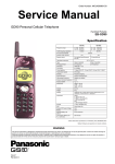
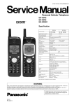
![ÿþs mv ½eå]û0ÖSqb¬− føfP 1](http://vs1.manualzilla.com/store/data/006594046_2-2209192e2508c1d6e49a82d5a3594049-150x150.png)
