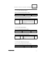
1
STP2002QFP
Revision 1.0–April 1996
STP2002QFP
Fast Ethernet, Parallel Port, SCSI
(FEPS)
USER’S GUIDE
OVERVIEW
1
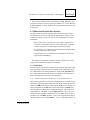
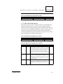
1.1 Introduction
The STP2002QFP FEPS (Fast Ethernet®, Parallel, SCSI) is an ASIC that provides integrated high-performance SCSI, 10/100 Base-T Ethernet, and a Centronics compatible parallel port.
1.2 Features
FEPS features include the following:
• IEEE 1496 SBus master interface with support for 64-bit mode access
• IEEE 1496 SBus slave interface, 32-bit mode only
• 20 MB/s fast and wide single-ended SCSI using a QLogic FAS366 core
• 10/100-Mb/sec Ethernet on the motherboard
• MII (Media Independent Interface) interface to support external transceivers
• DMA2-compatible Centronics parallel port with a maximum throughput of 4
MB/s
• Supports use on an SBus card device
• Provides a path to an FCode PROM for use on SBus boards
• JTAG support for boundary and internal scan testing
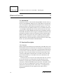
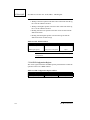
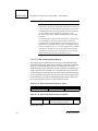
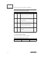
1.3 Overview
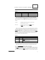
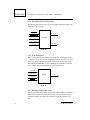
FEPS contains four major blocks: SBus Adapter (SBA), SCSI_Channel,
ENET_Channel, and PP_Channel. Each channel uses the Channel Engine In-
STP2002QFP
Fast Ethernet, Parallel Port, SCSI (FEPS) - STP2002QFP
terface (CEI) for slave and DMA transfers with the SBus (via SBA). The SBA
provides buffering and bus conversion between the SBus and the channel engine interface. Interrupts from the channel engine go directly to the SBus. The
SBA contains no software-accessible registers.
The channel engine interface provides a common interface to the three
channel engines thus reducing verification time. This interface limits the
amount of “awareness” that the SBA has concerning DMA transactions.
The SBA supports only 32-bit programmed I/O on the SBus. There are two
64-byte DMA write buffers, to allow buffered writes. A round-robin arbitration scheme will be used between the three channel engines.
The SCSI_Channel contains the SCSI DVMA and the FAS366. The SCSI
channel can perform 64-bit SBus DMA transfer. The SCSI DVMA provides
the two 64-byte buffers to transfer data to/from FAS366. The FAS366 allows
for a 16-bit SCSI data path and a throughput of 20 Mbytes/sec. The programming model of the SCSI DVMA follows the DMA2’s SCSI. All programmed
I/O access to the FAS366 is driven by the SCSI DMA.
The Ethernet DMA can perform 64-bit SBus DMA transfers.The Ethernet
DMA has two 2K-byte FIFOs (one for transmit and one for receive). The
transmit portion of the Ethernet DMA can assist in TCP checksum generation. This requires the entire frame to be loaded into the TxFIFO before the
checksum can be inserted into the frame (that resides in the TxFIFO). The
receive portion of the Ethernet DMA can assist in checking the checksum of
an incoming frame. The receive DMA can also pass incoming frames from
the BigMac (Media Access Conmtroller) before the entire frame has been
buffered in the RxFIFO.
1.4 Technology Information
Technology features of FEPS are as follows:
• 240-pin PQFP
• 112K gates + 4K bytes dual-ported RAM
• 5-V operation only
• 1.5-W maximum power consumption
• 16–25-MHz SBus interface and parallel port, 40-MHz SCSI core, 25-MHz Fast
Ethernet core
• 48-mA SCSI, 16-mA MII direct interconnect-capable drivers
1.5 Compliance
This part is fully compliant with IEEE 1496 SBus, ANSI SCSI-2 X3T9.2/86-
2
Sun Microelectronics
Fast Ethernet, Parallel Port, SCSI (FEPS) - STP2002QFP
STP2002QFP
109 rev10h, ISO/IEC 8802-3, IEEE 802.3u 100 Base-T, IEEE 1149.1 (
JTAG), Centronics-protocol-compatible parallel port, and the Sun4u system
architecture.
Sun Microsystems,
3
STP2002QFP
Fast Ethernet, Parallel Port, SCSI (FEPS) - STP2002QFP
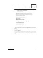
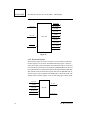
SBus
SBA
Channel Engine Interface
ENET_IRQ
SCSI_IRQ
PP_IRQ
SCSI DVMA
ENET DMA
PP DMA
FAS366
BigMac
PP Core
SCSI_Channel
SCSI
Bus
ENET_Channel
PP_Channel
MII
Interface
Boot PROM
Parallel Port
Figure 1. STP2002QFP Block Diagram
4
Sun Microelectronics
Fast Ethernet, Parallel Port, SCSI (FEPS) - STP2002QFP
STP2002QFP
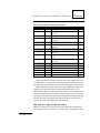
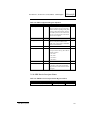
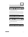
1.6 Pin Descriptions
The signal pins are grouped by function in the following tables.
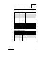
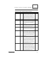
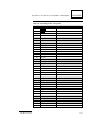
Table 1: SBus Signals
Signal Name
Type
Pin Count
Description
SB_D[31:0]
I/O
32
SBus data
SB_A[27:0]
I/O
28
SBus address
SB_SEL
I
1
SBus slave select
SB_BR
O
1
SBus DVMA request
SB_BG
I
1
SBus DVMA grant
SB_ACK[2:0]
I/O
3
SBus acknowledge codes
SB_SIZ[2:0]
I/O
3
SBus transfer size
SB_RD
I/O
1
SBus direction
SB_CLK
I
1
SBus clock
SB_RESET
I
1
SBus reset
SB_AS
I
1
SBus address strobe
SB_LERR
I
1
SBus late error
SB_DATAPAR
I/O
1
SBus data parity
SB_SC_INT
O
1
SCSI interrupt request to the system
SB_ET_INT
O
1
Ethernet interrupt request to the system
SB_PP_INT
O
1
Parallel port interrupt request to system
Total SBus
78
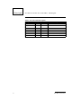
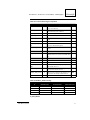
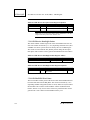
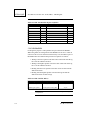
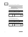
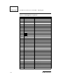
Table 2: SCSI Signals
Signal Name
Sun Microsystems,
Type
Pin Count
SCSI_D[15:0]
I/O
16
SCSI data
Description
SCSI_DP[1:0]
I/O
2
SCSI data parity
SCSI_SEL
I/O
1
SCSI select
SCSI_BSY
I/O
1
SCSI busy
SCSI_REQ
I/O
1
SCSI request
SCSI_ACK
I/O
1
SCSI acknowledge
SCSI_MSG
I/O
1
SCSI message phase
SCSI_CD
I/O
1
SCSI command/not data
SCSI_IO
I/O
1
SCSI direction
SCSI_ATN
I/O
1
SCSI attention
SCSI_RST
I/O
1
SCSI reset
5
STP2002QFP
Fast Ethernet, Parallel Port, SCSI (FEPS) - STP2002QFP
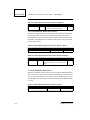
Table 2: SCSI Signals
Signal Name
Type
Pin Count
Description
SCSI_XTAL2
O
1
SCSI crystal output
SCSI_XTAL1
I
1
SCSI crystal input
POD
I
1
SCSI power detect
Total SCSI
30
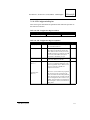
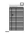
Table 3: Ethernet Signals
Signal Name
Pin Count
Description
ENET_TX_CLK
I
1
Ethernet transmit clock input
ENET_TXD[3:0]
O
4
Ethernet transmit data
ENET_TX_EN
O
1
Ethernet transmit enable
ENET_COL
I
1
Ethernet transmit collision detected
ENET_CRS
I
1
Ethernet carrier sense
ENET_RX_CLK
I
1
Ethernet receive clock
ENET_RXD[3:0]
I
4
Ethernet receive data
ENET_RX_DV
I
1
Ethernet receive data valid
ENET_RX_ER
I
1
Ethernet receive error
ENET_MDC
O
1
Ethernet management device clock
ENET_MDIO0
I/O
1
Ethernet management device I/O data for
on-board transceiver
ENET_MDIO1
I/O
1
Ethernet management device I/O data for
on-board transceiver
ENET_BUFFER_EN
_0
O
1
Ethernet buffer enable
ENET_TX_CLKO
O
1
Ethernet transmit clock output
Total Ethernet
6
Type
20
Sun Microelectronics
Fast Ethernet, Parallel Port, SCSI (FEPS) - STP2002QFP
STP2002QFP
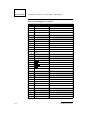
Table 4: Parallel Port Signals
Type
Pin Count
PP_DATA[7:0]
Signal Name
I/O
8
Parallel port data bus
Description
PP_STB
I/O
1
Parallel port data strobe
PP_BSY
I/O
1
Parallel port busy
PP_ACK
I/O
1
Parallel port acknowledge
PP_PE
I
1
Parallel port paper error
PP_SLCT
I
1
Parallel port select
PP_ERROR
I
1
Parallel port error
PP_INIT
O
1
Parallel port initialize/ALE high address byte
PP_SLCT_IN
O
1
Parallel port select in
PP_AFXN
O
1
Parallel port audio feed/ALE low address byte
PP_DSDIR
O
1
Parallel port data strobe direction
PP_BSYDIR
O
1
Parallel port busy direction
PP_ACKDIR
O
1
Parallel port ack direction
PP_DDIR
ID_CS
O
1
Parallel port data direction
I/O
1
ID PROM chip select
Total Parallel Port
22
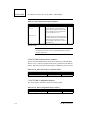
Table 5: JTAG/Miscellaneous Signals
Signal Name
Type
Pin Count
JTAG_TDO
O
1
JTAG test data out
JTAG_TDI
I
1
JTAG test data in
JTAG_TMS
I
1
JTAG test mode select
JTAG_CLK
I
1
JTAG clock
JTAG_RESET
I
1
JTAG TAP reset
STOP_CLOCK
I
1
Stop clock input
CLK_10M
O
1
10-MHz clock output
Total JTAG
Sun Microsystems,
Description
7
7
STP2002QFP
Fast Ethernet, Parallel Port, SCSI (FEPS) - STP2002QFP
Table 6: Power/Ground/Other Signals
Signal Name
VDD_CORE
8
Type
Pin Count
Description
4
VSS_CORE
4
VDD
21
VSS
52
Reserved
1
MODE
1
Total
83
Mode select (stand alone/chipset)
Sun Microelectronics
Fast Ethernet, Parallel Port, SCSI (FEPS) - STP2002QFP
STP2002QFP
SBUS ADAPTER
2
2.1 Introduction
The SBus Adapter (SBA) is the layer between the Channel Engine Interface
(CEI) and the SBus. It provides one master port on the SBus side to funnel
three DMA channel engines (CE) onto the SBus, and one slave port for SBus
accesses to the CEs. The SBA can be viewed as a block of data path and flow
control between SBus and channel engine interface.
2.2 SBus Capabilities
2.2.1 Slave Accesses
• Supports byte/half-word/word access, but not burst transfer
• Supports 32-bit transfer mode
• Parity generation/checking
• Does not generate late error
• Does not generate Rerun Ack
• Maximum latency < 22 SBus clocks
2.2.2 Master Accesses
• Compliant to IEEE 1496
• Supports 64-bit/32-bit transfer mode
• Supports byte/half-word/word transfer size
• Supports burst transfer size from 8 bytes to 64 bytes
• Parity generation/checking
• Does not issue atomic transaction
• Does not support bus sizing
2.2.3 Address Decoding
In order to eliminate the need of NEXUS driver in between FEPS device driver and the kernel there are no registers insides the SBA block (a register inside
SBA would be a global register which means a NEXUS driver is needed).
However, SBA does decode the physical address input and the access size for
Sun Microsystems,
9
STP2002QFP
Fast Ethernet, Parallel Port, SCSI (FEPS) - STP2002QFP
slave accesses from SBus. The physical address is decoded to select a target
CE to respond to the access. A physical address that cannot be resolved to the
selection of any channel engine will cause SBus Adapter to return Error Ack.
The access size is decoded to Error Ack 64-bit transfer mode or burst transfer
that is not supported by FEPS.
2.3 Theory of Operation
2.3.1 Master Operations
All master operations are originated from the channel engines. The operations
start when one or more bus requests are asserted on the channel engine interface.
2.3.1.1 DVMA Write
DVMA write cycle starts when the channel engine with highest priority asserts BR signal on CEI with RD (bit[63] of CE_DOUT signal) signal de-asserted. The arbiter inside SBA asserts grant signal (BG) to the requesting CE
and kick off the CEI write state machine. CEI write state machine first latches
the DVMA address, transfer size and channel ID from the requesting CE and
then begin to move data from CEI and write them to the current DVMA data
write buffer. When the whole burst of write data are written to the write buffer, the CEI state machine places a write request into the request command
queue of the SBus Master Port State machine and, at the mean time, it release
the arbiter to arbitrate the next request on the CEI. The master port state machine wakes up and requests the SBus whenever there is a request in the
queue. When the whole burst of Data is written to the SBus, the master port
state machine return the acknowledgment (MEMDONE) and status
(CE_DWERR) to the corresponding CE.
When a CE is granted for DMA write, the CEI bus is locked until the whole
burst of write data is moved over to the write data buffer. During this period,
only the slave write operation from the SBus can occur on the CEI. A slave
read would have to wait until the DMA write cycle is done. On the other hand,
a slave read operation will have the same effect as DMA write that will also
lock up the CEI for the duration of the whole transaction.
2.3.1.2 DVMA Read
DVMA Read cycle starts with the highest priority channel engine asserts BR
signal on CEI with RD (bit[63] of CE_DOUT signal) signal asserted. The arbiter latches the DVMA address, transfer size and channel ID and places a
Read request into the request command queue of the SBus master port state
10
Sun Microelectronics
Fast Ethernet, Parallel Port, SCSI (FEPS) - STP2002QFP
STP2002QFP
machine. After this the arbiter is available to arbitrate and grant the next request on the CEI provided that there is a DMA write or read buffer still available. The master port state machine wakes up and request the SBus whenever
there is a request in the queue. When SBus is granted, the master port state
machine asserted BG to the corresponding CE and pass the read data over to
the CEI bus.
2.3.2 Slave Operation
When both AS and SEL input signals are asserted, the slave port begin to respond to the slave access from the SBus. Based on the physical address, one
of the channel engines is selected to respond to the slave access. Slave writes
goes directly through to the CEI bus without arbitration because it share the
CEI data-in data bus with DVMA read which is mutually exclusive to slave
operation. Slave reads share the CEI data-out bus with all other CEI operations and have to go through arbiter to compete with channel engines.
Because a SBus DVMA read operation may encounter a retry, there is condition that a CE is being granted with DVMA read and a slave access still
comes in. The CE has to make sure that it can still respond to this slave access
under this condition.
Sun Microsystems,
11
STP2002QFP
Fast Ethernet, Parallel Port, SCSI (FEPS) - STP2002QFP
SCSI CHANNEL
3
3.1 Introduction
The SCSI channel consists of SCSI DVMA (also referred to as SCSI channel
engine) and FAS366, a “Fast and Wide” SCSI controller core. The SCSI
DVMA provides two 64-byte buffers used to transfer data to/from the
FAS366. The FAS366 supplies a 16-bit SCSI data path and a throughput of
20 MB/sec. All programmed I/O access to the FAS366 is driven by the SCSI
DVMA.
Several programmable registers can be used by the SCSI device driver to
direct the SCSI engine and FAS366 to move blocks of data to/from host
memory or to/from devices on the SCSI bus. Once the transfer is complete,
an interrupt is generated on the SBus to inform the driver that block movement is complete, freeing it to initiate further transfers.
3.2 SCSI DVMA
SCSI DVMA is responsible for data movement between FAS366 and the host
memory. It contains two 64-byte buffers. The purpose for providing these
buffers is to have prefetch capability. With this scheme of prefetch buffers,
one buffer can be used for writing/reading data on SBus, while the other buffer can be used for reading/writing data from/to FAS366. For SCSI write operation (reading from host memory and writing to FAS366), a chunk of data
is moved from the host memory and stored in the buffers. When FAS366 is
ready to accept data, this data is written to FAS366. For SCSI read operation
(reading from FAS366 and writing to host memory), data being read from
FAS366 is stored in the buffers. This data is written into host memory at a later time. The whole idea of providing buffers is to absorb the difference in data
transfer rate, between SBus and SCSI bus.
3.3 FAS366
FAS366 is a Fast and Wide SCSI controller core and is integrated into FEPS
as a hard macro.
The following are some of the features of the FAS366 core:
• Supports ANSI X3T9.2/86-109 (SCSI-2) standard
• Sustained SCSI data transfer rates:
- 10-MHz synchronous (fast SCSI)
12
Sun Microelectronics
Fast Ethernet, Parallel Port, SCSI (FEPS) - STP2002QFP
STP2002QFP
- 5-MHz synchronous (normal SCSI)
- 6-MHz asynchronous
• REQ/ACK programmable assertion/deassertion control
• Power-on connect/disconnect to SCSI bus (hot plugging)
• Target block transfer sequence
• Initiator block transfer sequence
• Bus idle timer
• Reduced SCSI bus overhead
• On-chip, single-ended SCSI drivers (48 mA)
• Target and initiator modes
• 16-bit recommand counter
• Differential mode support
For more information on FAS366, refer to the FAS366 specification from
Emulex.
3.4 Test Support
The SCSI DVMA will support full internal and boundary scan. The FAS366
core does not support full internal scan. SCSI I/O pads will support boundary
scan.
Sun Microsystems,
13
STP2002QFP
Fast Ethernet, Parallel Port, SCSI (FEPS) - STP2002QFP
PARALLEL PORT CHANNEL
4
4.1 Introduction
The parallel port interface implementation of FEPS is almost identical to the
one on the STP2000 Master I/O controller chip to leverage the existing device
driver. The only difference is that the DIR bit has to be set during a memory
clear operation. It allows the CPU to send data to the standard Centronics
printer in both programmed I/O and DMA modes. The parallel interface can
support bidirectional transfers using Xerox and IBM schemes. A 64-byte
buffer is used to buffer data to and from the channel engine interface and the
parallel port in DMA mode, depending on the direction of the transaction. In
synchronous mode, the port can support data transfer rate up to 4 Mbytes/s.
The parallel port interface also provides the data path to read the FCode
PROM when the FEPS chip is used on a SBus extended card. Two external
8-bit latches are needed to latch the MSB and LSB of the EPROM address.
Refer to the FEPS Application note for more details on this mode.
4.2 Parallel Port FIFO Operation
Between the parallel port and the SBus interface is a 64-byte FIFO (P_FIFO).
This FIFO is bypassed for slave accesses to the parallel port registers. Consistency control ensures that all data written by the external device gets to
main memory in a deterministic manner, and is handled completely in hardware. One of the consistency control mechanisms used on transfers to memory is draining of all P_FIFO data upon the access of any parallel port register.
The conditions that cause data in the P_FIFO to be drained to memory are
as follows:
14
1.
4, 16, or 32 bytes (depending on P_BURST_SIZE) have been
written into the P_FIFO.
2.
The P_INT_PEND bit in the P_CSR is set.
3.
The CPU does a slave write to a parallel port internal register
other than the P_TST_CSR (writing P_ADDR does not cause
draining if P_DIAG is set).
4.
The P_RESET or P_INVALIDATE bit in the P_CSR is set.
5.
The P_ADDR register is loaded from P_NEXT_ADDR when
P_DIAG is not set.
Sun Microelectronics
Fast Ethernet, Parallel Port, SCSI (FEPS) - STP2002QFP
STP2002QFP
None of these conditions will cause draining if P_ERR_PEND = 1, indicating that a memory error has occurred. If condition 4 or 5 occurs when the
P_ERR_PEND bit is 1, the P_FIFO will be invalidated and all dirty data will
be discarded.
4.3 Bidirectional Parallel Port Interface
The parallel port can operate unidirectionally or bidirectionally in either a
programmed I/O mode or in a DMA mode. The hardware interface can be
configured to operate with a wide range of devices through the following
mechanisms:
• Bidirectional signal configuration for the interface control signals—
data strobe, acknowledge, and busy. Each control signal can be individually configured as a unidirectional or bidirectional signal.
• Programmable pulse widths for all generated signals and programmable data setup time for data transfers.
• Programmable protocol definition for all combinations of acknowledge and busy handshaking.
This interface configuration capability will allow operation over a wide
range of data transfer rates and protocol definitions.
4.3.1 DMA Mode
Since no software intervention is required for data transfer, the interface protocol and timing required must be programmed via the configuration registers. DMA transfers are initiated/enabled by setting the P_EN_DMA bit of
the P_CSR. The operation of the interface is dependent on the direction of
transfer and the protocol selected as described below.
4.3.1.1 Unidirectional Operation (Transfers to the Peripheral Device)
This mode of operation is the Centronics implementation of a unidirectional
parallel port. Operation of the parallel port in this mode requires the direction
control bit (DIR) of the transfer control register (TCR) to be 0. Timing variations are handled via the DSS (data setup to data strobe) and DSW (data
strobe width) bits of the hardware configuration register. The timebase for
programmability is the SBus clock. The DSS parameter (7 bits) can be programmed from a minimum of 0 SBus clocks to 127 SBus clocks in steps of
one SBus clock. The DSW parameter (7 bits) is also programmed in steps of
one SBus clocks, however when DSW= 0, 1, 2, or 3, data strobe width is de-
Sun Microsystems,
15
STP2002QFP
Fast Ethernet, Parallel Port, SCSI (FEPS) - STP2002QFP
fined as three SBus clocks. That is, the minimum data strobe width is three
SBus clocks. The following table shows the nominal range of programmability for different SBus clock speeds.
16
Sun Microelectronics
STP2002QFP
Fast Ethernet, Parallel Port, SCSI (FEPS) - STP2002QFP
Table 7:
SBus Clock
DSS
DSW
16.67 MHz
0–7.62 µs
180.0 ns–7.62 µs
20 MHz
0–6.35 µs
150.0 ns–6.3 µs
25 MHz
0–5.08 µs
120.0 ns–5.08 µs
The desired handshake protocol can be selected using the ACK_OP
(acknowledge operation) and BUSY_OP (busy operation) bits of the operations configuration register (OCR). The function of these bits is defined as
follows:
ACK_OP
1 = Handshake complete with receipt of P_ACK (PP_ACK).
0 = P_ACK (PP_ACK) is ignored.
BUSY_OP
1 = Handshake complete with receipt of P_BSY (PP_BSY).
0 = P_BSY (PP_BSY) is not used for handshaking.
These two bits allow selection of one of four possible protocols, however
only three of these protocols make sense and are valid selections. The case of
ACK_OP=BUSY_OP=1, is not supported. For all protocol selections, if
P_BSY (PP_BSY) is active, further data transfers will not occur until P_BSY
(PP_BSY) is negated. The following table summarizes the protocol definitions for transfers to the peripheral device.
Table 8:
BUSY_OP
ACK_OP
0
0
Protocol Definition
0
1
Acknowledge is required for each byte transferred
1
0
P_BSY is used as acknowledge and is required for each byte
transferred. ACK is ignored
1
1
Invalid
No handshaking occurs
The transfer modes are shown and discussed in the following sections.
4.3.1.1.1 No Handshake (BUSY_OP=0, ACK_OP=0)
Data transfers are controlled by the use of P_D_STRB (PP_STB) and optionally P_BSY (PP_BSY). There is no acknowledge in this mode and P_ACK
(PP_ACK) is a don’t care. P_BSY (PP_BSY) is used to gate further transfers
Sun Microsystems,
17
STP2002QFP
Fast Ethernet, Parallel Port, SCSI (FEPS) - STP2002QFP
when the peripheral device cannot receive another byte of data. P_BSY
(PP_BSY) is sampled before data strobe becomes active and after data strobe
becomes inactive, to ensure that a data transfer is not attempted while the device is busy.
It is this mode, which provides the fastest transfer of data over the interface, the fastest cycle time is six SBus clocks per byte. This transfer time is
arrived at as follows: DSS=0, DSW=3 (minimum width of DSW is three
SBus clocks), and three SBus clocks between consecutive data strobes. This
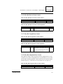
assumes that P_BSY (PP_BSY) is not asserted during the transfer cycle. Reference Figure 2.
P_DATA (O)
1
P_D_STRB (O)
P_ACK (I)
DSS
2
DSW
3
1
DSS
2
DSW
5
4
Don’t Care
P_BSY (I)
1. Data setup as defined in the hardware configuration register.
2. Data strobe width as defined in the hardware configuration register.
3. There is a three SBus clock delay from the end of data strobe to the next byte of data being clocked onto the P_DATA
bus.
4. Acknowledge is a don’t care condition for all data transfers.
5. When P_BSY is active, it gates further data transfers.
Figure 2.
4.3.1.1.2 Handshake with Ack: BUSY_OP=0, ACK_OP=1)
Data transfers are controlled by the use of P_D_STRB (PP_STB), P_ACK
(PP_ACK), and optionally P_BSY (PP_BSY). P_ACK (PP_ACK) is required for each byte transferred. If P_BSY (PP_BSY) is active at the end of
the cycle, further data transfers will be gated until P_BSY (PP_BSY) becomes inactive. If P_BSY (PP_BSY) is not present, then data transfers will
proceed. P_BSY (PP_BSY) is also sampled immediately before P_D_STRB
(PP_STB) is generated to ensure that a data transfer is not attempted while the
device is busy. Reference the data transfer diagram in Figure 3.
18
Sun Microelectronics
STP2002QFP
Fast Ethernet, Parallel Port, SCSI (FEPS) - STP2002QFP
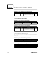
P_DATA (O)
P_D_STRB
1
DSS
2
DSW
5
(O)
3
P_ACK (I)
4
1. Data setup as defined in the hardware configuration register.
2. Data strobe width as defined in the hardware configuration register.
3. Acknowledge is required for each byte transferred.
4. When P_BSY is active, it gates further data transfers.
5. If P_BSY is not present, the next data byte will be gated on to the bus following ACK (there is a minimum of three SBus clocks between
the trailing edge of ACK and the next data byte).
6. All signal polarities shown are at the HIOD pins. Polarities on the interface cable should be inverted (except P_DATA).
Figure 3.
4.3.1.1.3 Handshake with Busy (ACK_OP=0, BUSY_OP=1)
Data transfers are controlled by the use of P_D_STRB (PP_STB) and P_BSY
(PP_BSY). P_ACK (PP_ACK) is a don’t care in this mode. P_BSY
(PP_BSY) is required as an acknowledge after P_D_STRB (PP_STB) and
will gate any further data transfers while it is active. P_BSY (PP_BSY) is also
sampled immediately before P_D_STRB (PP_STB) is generated to ensure
that a data transfer is not attempted while the device is busy. Reference the
data transfer diagram in Figure 4.
P_DATA (O)
P_D_STRB
1
DSS
2
DSW
5
(O)
3
Don’t Care
P_ACK (I)
4
1. Data setup as defined in the hardware configuration register.
2. Data strobe width as defined in the hardware configuration register.
3. Acknowledge is a don’t care condition for all data transfers.
4. P_BSY is required as an acknowledge for each byte transferred. While P_BSY is present, it gates fuirther data transfers.
5. The next byte of data will be gated on to the bus following the trailing edge of P_BSY (there is a minimum of three SBus clocks between
the trailing edge of P_BSY and the next byte of data).
6. All signal polarities shown are at the HIOD pins. Polarities on the interface cable should be inverted (except P_DATA).
Figure 4.
Sun Microsystems,
19
STP2002QFP
Fast Ethernet, Parallel Port, SCSI (FEPS) - STP2002QFP
4.3.1.2 Bidirectional Operation
Bidirectional data transfer over the parallel port can be accomplished by the
use of either of two master/slave protocols. The “master write” protocol or the
“master read/write” protocol. The IBM implementation of a bidirectional parallel port uses the master write protocol in which the master always writes
data to the slave and when the direction of data transfer needs to be reversed,
mastership is exchanged. The Xerox implementation uses the master
read/write protocol where data transfer is performed in either direction under
control of the fixed master. The parallel port will operate as either master or
slave when configured for master write protocol, and only as the master when
configured for the master read/write protocol.
The selection of one of these bidirectional transfer methods is accomplished indirectly through the specification of the bidirectional nature of the
data strobe signal. Since in both methods data strobe resides with the master,
a bidirectional data strobe implies the IBM master write scheme and a fixed
data strobe (output only) implies the Xerox master read/write scheme.
The interface control signals—data strobe, acknowledge, and busy—are
individually configurable as bidirectional or unidirectional pins. The bidirectional signal configuration bits are located in the operation configuration
register. The functions of the bits are as follows:
DS_DSEL
1 = P_DS (PP_DSDIR) is bidirectional, master write protocol selected.
0 = P_DS (PP_DSDIR) is fixed as output. Master read/write protocol
selected.
ACK_DSEL
1 = P_ACK (PP_ACK) is bidirectional.
0 = P_ACK (PP_ACK) is fixed as an input.
BUSY_DSEL
1 = P_BSY (PP_BSY) is bidirectional.
0 = P_BSY (PP_BSY) is fixed as an input.
To allow external driver/receiver connection, each of these control signals
and the data bus has a corresponding direction control pin. The DIR bit of the
transfer control register is used to switch the direction of the data bus and the
pins that have been configured as bidirectional. The state of the DIR bit is
reflected on the P_D_DIR (PP_DDIR) pin for external transceiver control
and direction control communication to the attached device. While DIR=0,
all pins remain in their unidirectional sense which is defined to be consistent
with the unidirectional parallel port as follows:
20
Sun Microelectronics
Fast Ethernet, Parallel Port, SCSI (FEPS) - STP2002QFP
STP2002QFP
Table 9:
Signal
P_D_STRB (PP_STB)
I/O
DIR_Pin
O
P_DS_DIR (PP_DSDIR)
State
1
P_ACK (PP_ACK)
I
P_ACK_DIR (PP_ACKDIR)
0
P_BSY (PP_BSY)
I
P_BSY_DIR (PP_BSYDIR)
0
P_DATA (PP_DATA)
O
P_D_DIR (PP_DDIR)
1
When DIR is set to 1, the pins configured as bidirectional change direction
and their corresponding direction control pins are set accordingly. Note that
the input status pins (ERR, SLCT, PE), which are readable in the input register, are not configurable. They are fixed as inputs. Similarly, the output pins
(PP_AFXN, PP_INIT, PP_SLCT_IN) of the output register are fixed as
outputs.
The transfer modes are shown and discussed in the following sections.
4.3.1.3 Master Write Protocol, Slave Operation
This section describes the parallel port operation as a slave when it is configured for master write protocol (DS_DSEL=1). Operation as a master is the
same as is described in the “Unidirectional Operation (Transfers to the Peripheral Device)” section on page 15.
In this mode, acknowledge and/or busy can be generated in response to a
data strobe. The width of the P_ACK (PP_ACK) pulse can be defined using
the DSW bits of the hardware configuration register. The P_BSY (PP_BSY)
hold time and P_ACK (PP_ACK) positioning after the trailing edge of data
strobe are defined using the DSS bits. However, note that in this mode DSS
has a tolerance of +3 to 4 SBus clocks, due to synchronization delays. The
nominal programmability range is the same as was specified in the “Unidirectional Operation (Transfers to the Peripheral Device)” section on page 15.
The ACK_OP and BUSY_OP bits are used to specify handshake protocol.
The function of the bits take on a new meaning when the parallel port is a
slave.
ACK_OP
1 = Generate P_ACK (PP_ACK) in response to a data strobe.
0 = P_ACK (PP_ACK) is not generated. P_ACK is held in an inactive state.
BUSY_OP
1 = Generate P_BSY (PP_BSY) as an acknowledge, in response to data strobe.
0 = P_BSY (PP_BSY) is not generated for each byte transferred, but is asserted
as required.
Sun Microsystems,
21
STP2002QFP
Fast Ethernet, Parallel Port, SCSI (FEPS) - STP2002QFP
These two bits allow selection of one of four possible handshake protocols.
The following table summarizes the protocol definitions for transfers to the
parallel port from the peripheral device.
For all protocol selections, P_BSY (PP_BSY) will become active if one of
the following conditions occur: The P_DMA_ON bit is reset indicating
DMA cannot proceed; or the
P_FIFO is unable to accept more data. Internally, P_BSY (PP_BSY) will
always be generated for these conditions. However, if the P_BSY (PP_BSY)
pin is not configured as an output, it will not be driven and the external interface will not be able to detect the busy condition. In this case, data could be
lost. In all cases, if P_BSY (PP_BSY) is asserted it will have the following
timing characteristics:
P_D_STRB
(I)
1
2
DSS
1. WHen data strobe is detected, P_BSY will be generated within 3 SBus clocks, if required.
2. P_BSY hold time after data strobe is configurable via DSS.
Figure 5.
The transfer modes are shown and discussed in the following sections.
4.3.1.3.1 No Handshake: (BUSY_OP=0, ACK_OP=0)
No handshake signals are generated in this mode. If P_ACK (PP_ACK) is
configured as an output, it will remain low or inactive. P_BSY (PP_BSY) will
be generated as required to gate further transfers, but not as a handshake signal. The operation of the interface as defined assumes the bidirectional sense
of each signal has been configured as follows: DIR=1, DS_DSEL=1,
ACK_DSEL=X, BUSY_DSEL=1. If P_ACK (PP_ACK) is configured as
an output, it will remain low or inactive. The configuration of P_BSY
(PP_BSY) as an output is suggested to avoid potential data loss. Reference
the parallel port timing section for detailed timing requirements for this mode.
4.3.1.3.2 Handshake with ACK: (BUSY_OP=0, ACK_OP=1)
Data transfers are acknowledged using P_ACK (PP_ACK). The position of
P_ACK (PP_ACK) relative to the trailing edge of data strobe is set using
DSS. Note that in this mode, the actual positioning of P_ACK (PP_ACK) will
be DSS plus 3 to 4 SBus clocks, due to synchronization delays. The width of
P_ACK (PP_ACK) is set using DSW. P_BSY (PP_BSY) will be generated
22
Sun Microelectronics
Fast Ethernet, Parallel Port, SCSI (FEPS) - STP2002QFP
STP2002QFP
as required to gate further transfers but not as a handshake signal. The operation of the interface as defined assumes the bidirectional sense of each signal
has been configured as follows: DIR=1, DS_DSEL=1, ACK_DSEL=1,
BUSY_DSEL=1. The configuration of P_BSY (PP_BSY) as an output is
suggested to avoid potential data loss. Reference the data transfer diagram in
Figure 6.
P_DATA (I)
P_D_STRB
1
DSS
(I)
2
DSW
P_ACK (O)
3
1. Acknowledge position relative to data strobe (DSS - hardware configuration register).
2. Acknowledge width (DSW - hardware configuration register).
3. P_BSY will be asserted if required.
4. All signal polarities shown are at the HIOD pins. Polarities on the interface cable should be inverted (except P_DATA).
Figure 6.
4.3.1.3.3 Handshake with BUSY: (BUSY_OP=1, ACK_OP=0)
Data transfers are acknowledged using P_BSY (PP_BSY). P_BSY
(PP_BSY) will be generated off of the leading edge of P_D_STRB (PP_STB)
and will remain active for the period specified by DSS (plus 3 to 4 SBus
clocks) beyond the end of P_D_STRB (PP_STB). The operation of the interface as defined assumes the bidirectional sense of each signal has been configured as follows: DIR=1, DS_DSEL=1, ACK_DSEL=X,
BUSY_DSEL=1. The configuration of P_ACK as an input will not hinder the
operation of the interface as far as handshaking is concerned. If P_ACK is
configured as an output, it will remain low or inactive. Reference the data
transfer diagram Figure 7.
Sun Microsystems,
23
STP2002QFP
Fast Ethernet, Parallel Port, SCSI (FEPS) - STP2002QFP
P_DATA (I)
P_D_STRB
(I)
Logic 0
P_ACK (O)
1
DSS
1. P_BSY hold time after data strobe (DSS - hardware configuration register)
2. All signal polarities shown are at the HIOD pins. Polarities on the interface cable should be inverted (except P_DATA).
Figure 7.
4.3.1.3.4 Handshake with ACK and BUSY: (BUSY_OP=1, ACK_OP=1)
Both P_ACK (PP_ACK) and P_BSY (PP_BSY) are generated in response to
a data strobe. P_BSY (PP_BSY) will be generated off of the leading edge of
P_D_STRB (PP_STB) and will remain active for 3 SBus clocks beyond the
end of P_ACK (PP_ACK). The position of P_ACK (PP_ACK) relative to the
trailing edge of data strobe is defined by DSS (again DSS has a tolerance of
+3 to 4 SBus clocks). The width of P_ACK (PP_ACK) is set using DSW. The
operation of the interface as defined assumes the bidirectional sense of each
signal has been configured as follows: DIR=1, DS_DSEL=1,
ACK_DSEL=1, BUSY_DSEL=1. Reference the data transfer diagram in
Figure 8.
P_DATA (I)
P_D_STRB
(I)
1
DSS
P_ACK (O)
2
DSW
3
1. Acknowledge position relative to data strobe (DSS - hardware configuration register).
2. Acknowledge width (DSW - hardware configuration register).
3. P_BSY is deasserted 3 SBus clocks following the trailing edge of ACK.
4. All signal polarities shown are at the HIOD pins. Polarities on the interface cable should be inverted (except P_DATA).
Figure 8.
24
Sun Microelectronics
Fast Ethernet, Parallel Port, SCSI (FEPS) - STP2002QFP
STP2002QFP
4.3.1.4 Master Read/Write Protocol (Xerox Mode)
This section describes the parallel port operation while master read cycles are
performed. Operation while master write cycles are performed is the same as
is described in the “Unidirectional Operation (Transfers to the Peripheral Device)” section on page 15.
Data transfer for master read cycles is accomplished by the master generating a data strobe (request for data) with no data present on the P_DATA
(PP_DATA) bus. The peripheral responds by placing data on the P_DATA
(PP_DATA) bus and generating an P_ACK (PP_ACK) which functions as a
strobe. Only one handshake protocol is valid for master read cycles and is
described below.
4.3.1.4.1 Handshake with ACK: (BUSY_OP=0, ACK_OP=1)
Data is transferred to the HIOD by the use of P_ACK (PP_ACK).
P_D_STRB (PP_STB) width is defined by DSW. DSS is used to define the
required interval from P_ACK (PP_ACK) to the next P_D_STRB (PP_STB).
P_BSY (PP_BSY) will gate further data transfers if present. The operation of
the interface as defined assumes the bidirectional sense of each signal has
been configured as follows: DIR=1, DS_DSEL=0, ACK_DSEL=0,
BUSY_DSEL=0. Reference the data transfer diagram in Figure 9.
P_DATA (I)
P_D_STRB
2
DSS
1
DSW
(O)
3
P_ACK (I)
4
1. Data strobe width as defined in the hardware configuration register.
2. DSS is used for ACK to P_D_STRB stiming (Hardware configuration register).
3. Acknowledge is used as a strobe and is required for each byte transferred.
4. If P_BSY is active, it gates further data transfers.
5. All signal polarities shown are at the HIOD pins. Polarities on the interface cable should be inverted (except P_DATA).
Figure 9.
4.3.2 Programmed I/O Mode
Programmed I/O mode is intended to allow the parallel port to operate primarily under software control. Data latching, interrupt, and busy generation are
performed in hardware as required. The following two sections describe opSun Microsystems,
25
STP2002QFP
Fast Ethernet, Parallel Port, SCSI (FEPS) - STP2002QFP
eration for transfers to and from the peripheral device.
4.3.2.1 PIO on Transfers to the Peripheral Device
For transfers to the peripheral device, all signals are under the control of software. There is no hardware assist other than interrupt generation.
4.3.2.2 PIO on Transfers From the Peripheral Device
The two modes of bidirectional operation previously discussed are supported
with hardware-assisted data latching. The bidirectional select bits
(DS_DSEL, ACK_DSEL, BUSY_DSEL) should be set according to the desired configuration. The handshake protocol bits (ACK_OP, BUSY_OP)
have no function in PIO mode.
During operation as a slave under the master write protocol (DS_DSEL=1,
DIR=1), data is sampled and latched once data strobe has been detected.
P_BSY (PP_BSY) becomes active at the same time that data is latched and
must be made inactive under software control.
During operation under master read/write protocol (DS_DSEL=0,
DIR=1), master reads are assisted by sampling and latching the data once
P_ACK (PP_ACK) has been detected. P_BSY (PP_BSY) is not generated in
this mode.
26
Sun Microelectronics
Fast Ethernet, Parallel Port, SCSI (FEPS) - STP2002QFP
STP2002QFP
4.4 Differences from STP2000 (MACIO) Parallel Port
• PP_INIT and PP_AFXN have extra functions: high and low address
latch clocks
• EPROM address is given by parallel port data bus
• DIR bit in the TCR register must be set during memory clear operation
4.5 Test Support
The TST_CSR provides a way for the user to test the DMA engine. The test
consists of moving one block data of the size of a read burst from the host
memory into the FIFO. The user then instructs the engine to drain data back
to the host memory at an address which is programmable.
The maximum size of a read burst is 32 bytes. Since the starting address of
the FIFO register cannot be programmed, the user has no control over which
FIFO registers should be tested. And since the maximum size of the burst is
limited to 32 bytes, the entire FIFO (64 bytes) cannot be tested.
Sun Microsystems,
27
STP2002QFP
Fast Ethernet, Parallel Port, SCSI (FEPS) - STP2002QFP
ETHERNET CHANNEL
5
5.1 Introduction
The Ethernet channel is a dual-channel intelligent DMA controller on the system side, and an IEEE 802.3 Media Access Control (MAC) on the network
side. It is designed as a high-performance full-duplex device, allowing for simultaneous transfers of data from/to host memory to/from the “wire.” The
two main functions of the Ethernet channel are to provide MAC function for
a 10-/100-Mbps CSMA/CD protocol based network and to provide a highperformance two-channel DVMA host interface between the MAC controller
and the SBus. The Ethernet channel supports 10/100-Mbit Fast Ethernet. The
Fast Ethernet standard is backwards compatible with the standard 10-Mb/s
Ethernet standard. The speed is auto-sensed. An RJ-45 connector supports
twisted-pair style of Ethernet. In addition, a Media Independent Interface
(MII) connection is supported through an external transceiver to allow adaptation to any other form of Ethernet (AUI/TP/ThinNet).
5.2 Functional Description
5.2.1 Overview
Packets scheduled for transmission are transferred over the SBus into a local
transmit FIFO and are later transferred to the TX_MAC core for protocol processing and transmission over the medium. A programmable transmit threshold is provided to enable the transmission of the frame. The reverse process
takes place in the receive path. Packets received from the medium are processed by the RX_MAC, loaded into the receive FIFO, and are later transferred to the host memory over the SBus. The receive threshold for data
transfers is 128 bytes.
At the device driver level, the user deals with transmit and receive descriptor-ring data structures for posting packets and checking status. In the
transmit case, packets may be posted to the hardware in multiple buffers
(descriptors), and the transmit DMA engine will perform “data gather.” In the
receive case, the receive DMA engine will store an entire packet in each
buffer that was allocated by the host. “Data scatter” is not supported, but
instead a programmable first byte-alignment offset within a burst is
implemented.
28
Sun Microelectronics
Fast Ethernet, Parallel Port, SCSI (FEPS) - STP2002QFP
STP2002QFP
For TCP packets, hardware support is provided for TCP checksum computation. On transmit, it is assumed that the entire packet is loaded into the local
FIFO before its transmission begins. The checksum is computed on-the-fly
while the packet is being transferred from the host memory into the local
FIFO. The checksum result is then stuffed into the appropriate field in the
packet, and the transmission of the frame begins. On receive, checksum is
computed on the incoming data stream from the MAC core, and the result is
posted to the device driver as part of the packet status in the descriptor.
5.2.2 Functional Blocks
The Ethernet channel is comprised of five major blocks:
• BigMAC core
• Management interface (MIF)
• Ethernet transmit (ETX)
• Ethernet receive (ERX)
• Shared Ethernet block (SEB)
5.2.2.1 BigMAC Core
The BigMAC core implements the IEEE 802.3 MAC protocol for 10-/100Mbps CSMA/CD networks. It consists of four major functional modules:
• Host interface buffer
Implements the programmed I/O interface between the SEB and BigMAC core
• Transmit MAC (TX_MAC)
- Implements the IEEE 802.3 transmit portion of the protocol
- Implements the slave interface handshake between the ETX and
TX_MAC for frame data transfers
- Performs the synchronization between the system clock domain and
the transmit media clock domain in the transmit data path
• Receive MAC (RX_MAC)
- Implements the IEEE 802.3 receive portion of the protocol
- Implements the slave interface handshake between the ERX and
RX_MAC for frame data transfers
- Performs the synchronization between the system clock domain and
the receive media clock domain in the receive data path
Sun Microsystems,
29
STP2002QFP
Fast Ethernet, Parallel Port, SCSI (FEPS) - STP2002QFP
• Transceiver interface (XIF)
- Implements the MII interface protocol (excluding the management
interface)
- Performs the nibble-to-byte and byte-to-nibble conversion between
the protocol engine and the MII
30
Sun Microelectronics
Fast Ethernet, Parallel Port, SCSI (FEPS) - STP2002QFP
STP2002QFP
5.2.2.2 Management Interface Function (MIF)
The management interface block implements the management portion of the
MII interface to an external transceiver, as defined in the IEEE 802.3 MII
specification.
It allows the host to program and collect status information from two
external transceivers connected to the MII. The MIF supports three modes of
operation.
Bit-Bang Mode
The Bit-Bang mode of operation provides maximum flexibility with minimum hardware support for the serial communication protocol between the
host and the transceivers. The actual protocol is implemented in software, and
the interaction with the hardware is done via three one-bit registers: data,
clock, and output_enable. Each read/write operation on a transceiver register
would require approximately 150 software instructions by the host.
Frame Mode
This mode of operation provides a much more efficient way of communication between the host and the transceivers. The serial communication protocol between the host and the transceivers is implemented in hardware, and the
interaction with the software is done via one 32-bit register (frame register).
When the software wants to execute a read/write operation on a transceiver
register, all it has to do is load the frame register with a valid instruction
(frame), and poll the valid bit for completion. The hardware will detect the
instruction, serialize the data, execute the serial protocol on the MII management interface and set the valid bit to the software.
Polling Mode
As defined in the IEEE 802.3u MII standard, a transceiver shall implement at
least one status register that will contain a defined set of essential information
needed for basic network management. Since the MII does not include an interrupt line, a polling mechanism is required for detecting a status change in
the transceiver. In order to reduce the software overhead, the above mentioned polling mechanism has been implemented in hardware. When this
mode of operation is enabled, the MIF will continuously poll a specified
transceiver register, and generate a maskable interrupt when a status change
is detected. Upon detection of an interrupt, the software can read a local status
register that will provide the latest contents of the transceiver register, and an
indication which bits have changed since it was last read. This mode of oper-
Sun Microsystems,
31
STP2002QFP
Fast Ethernet, Parallel Port, SCSI (FEPS) - STP2002QFP
ation can only be used when the MIF is in the frame mode.
5.2.2.3 Ethernet Transmit Block (ETX)
The Ethernet transmit block provides the DMA engine for transferring frames
from the host memory to the BigMAC. It contains a local buffer of 2K bytes
for rate adaptation between the available bandwidth on the SBus and on the
network.
5.2.2.4 Ethernet Receive Block (ERX)
The Ethernet receive block provides the DMA engine for transferring frames
from the BigMAC to the host memory. It contains a local buffer of 2K bytes
for rate adaptation between the available bandwidth on the network and on
the SBus.
5.2.2.5 Shared Ethernet Block (SEB)
The shared Ethernet block contains common functions that are shared between the ETX and ERX blocks. It performs the first level arbitration between the receive and transmit DMA channels for access to the SBus and
provides one common interface between the Ethernet channel and the SBus
adapter (SBA). It also separates the DMA data path from the programmed I/O
data path.
5.2.3 Clock Domains
The Ethernet channel contains three completely asynchronous clock domains.
System Clock Domain
The bulk of the logic in the Ethernet channel is driven off this clock. It is
sourced by the system bus and is defined to be in the range of 16.67 MHz
through 33.33 MHz.
Transmit Clock Domain
This clock is used to drive the transmit protocol engine in the BigMAC core.
It is sourced by the MII and has the operating frequency of 2.5/25 MHz 100
ppm. The 2.5/25 MHz version of this clock (TX_NCLK) is used for byte-tonibble conversion of the data stream to the MII and for synchronization of the
asynchronous signals from the MII (CRS and COLL). The 1.25/12.5 MHz divide-by-two version of this clock (TX_BCLK) is used for transmit protocol
processing and state machine operation.
32
Sun Microelectronics
Fast Ethernet, Parallel Port, SCSI (FEPS) - STP2002QFP
STP2002QFP
Receive Clock Domain
This clock is used to drive the receive protocol engine in the BigMAC core.
It is sourced by the MII and has the operating frequency of 2.5/25 MHz 100
ppm. The 2.5/25 MHz version of this clock (RX_NCLK) is used for strobing
in the packet data from the MII and for nibble-to-byte conversion of the incoming data stream. The 1.25/12.5 MHz divide-by-two version of this clock
(RX_BCLK) is used for receive protocol processing and state machine operation.
5.2.4 Host Memory Data Management
The device driver maintains two data structures in the host memory: one for
transmit and the other for receive packets. Both data structures are organized
as wrap-around descriptor rings. Each descriptor ring has a programmable
number of descriptors (in the range of 16 through 256). Each descriptor has
two entries (words): a control/status word and a pointer to a data buffer.
The interaction between the hardware and the software is managed via a
semaphore (OWN) bit, that resides in the control/status portion of the descriptor. When the OWN bit is set to 1, the descriptor is owned by the hardware.
If the OWN bit is cleared to 0, the descriptor is owned by the software. The
owner of the descriptor is responsible for releasing the ownership when it can
no longer use it. Once the ownership is released, the previous owner may no
longer treat the descriptor contents as valid, since the new owner may overwrite it at any time.
5.2.5 Transmit Data Descriptor Ring
A transmit packet that is posted by an upper layer protocol to the device driver
may reside in several data buffers (headers and data) which are scattered in
the host memory. When the device driver posts the packet to the hardware, it
allocates a descriptor for each buffer. The descriptor contains the necessary
information about the buffer that the hardware needs for the packet transfer.
When the packet is ready for transmission, the descriptor(s) ownership is
turned over to the hardware, and a programmed I/O command is issued to the
transmit DMA channel to start the packet transfer from the host memory to
the TxFIFO.
When the packet transfer has been completed, the transmit DMA channel
turns over the descriptor ownership back to the driver and polls the next
descriptor in the ring. If the descriptor is owned by the hardware, the next
packet transfer begins. If not, the DMA channel “goes to sleep” until a new
command is issued.
Sun Microsystems,
33
STP2002QFP
Fast Ethernet, Parallel Port, SCSI (FEPS) - STP2002QFP
The size of the descriptor ring is programmable, and it can be varied in the
range of 16–256 in increments of 16 descriptors: 16, 32, 48, ..., 240, 256.
5.2.6 Receive Free Buffer Descriptor Ring
For receive operation, the device driver requests a pool of free buffers from
the operating system. The buffers are posted to the hardware by allocating a
descriptor for each buffer. The descriptor contains the necessary information
about the buffer that the hardware needs for the packet transfer.
When a packet is ready to be transferred from the RxFIFO to the host memory, the receive DMA channel polls the next descriptor in the ring. If the
hardware owns the descriptor (free buffer available), the packet transfer
begins. During the first burst, the receive DMA engine performs header padding of the packet by inserting a programmable number of junk words at the
beginning of the packet.
When the packet transfer has been completed, the receive DMA channel
updates the descriptor with status information about the received packet, and
turns over the descriptor ownership back to the driver. If a packet is ready to
be transferred from the RxFIFO to the host memory but the driver does not
have any free buffers allocated to the hardware, the packet will be dropped
into the bit bucket, and the DMA channel will try again when the next packet
is ready to go.
The size of the descriptor ring is programmable and can assume the following values: 32, 64, 128, 256.
5.2.7 Local Memory Data Management
Each DMA channel contains its own dedicated on-chip local buffer of 2K
bytes (fixed) in size. The local buffers are used for temporary storage of packets en route to/from the network, and are organized as wrap-around FIFOs.
In general, the local buffer organization and data structures are invisible to
the software, except for diagnostic purposes.
Since the local buffers reside in the data path, their logical organization
changes depending on the SBus width. For a 32-bit SBus, the FIFO organization is 512 words × 33 bits. For a 64-bit SBus, the FIFOs are organized as 256
words × 65 bits. The extra bits (bit 33 or bit 65) along the word are used as
end-of-packet delimiters (or tags). When a packet is stored in the local buffer,
the tag will be cleared to 0 for the entire data portion of the packet, except for
the last word. The tag will be set to 1 for the last data word of the packet and
for the control/status word.
34
Sun Microelectronics
Fast Ethernet, Parallel Port, SCSI (FEPS) - STP2002QFP
STP2002QFP
5.2.8 Transmit FIFO Data Structures
When a transmit packet is transferred from the host into the local memory, the
first byte of the packet in the FIFO is always loaded to be word (or doubleword) aligned. If the packet is composed of several data buffers, the data buffers are concatenated as a contiguous byte stream in the FIFO (gather function). The last byte of a packet can reside at any byte boundary, therefore the
last data word of the packet is marked by a tag. At the end of the packet a control word is appended, which is again marked by a tag bit. The control word
indicates the last byte boundary for the packet.
5.2.9 Receive FIFO Data Structures
When a receive packet is transferred from the RX_MAC into the local memory, the half-word (16-bit) data stream is packed into words (or double
words), with the first byte of the packet starting at a programmable offset
within the first word.
Even though the receive data structure’s functionality does not require to
tag the last data word of a packet, the hardware will do that to provide a more
robust implementation.
At the end of the packet a status word is appended, which is again marked
by a tag bit. This word provides status information about the received frame,
which is either passed to the device driver or used for unloading the frame
from the RxFIFO.
Sun Microsystems,
35
STP2002QFP
Fast Ethernet, Parallel Port, SCSI (FEPS) - STP2002QFP
5.3 Error Conditions and Recovery
There are two types of error conditions that can be encountered during the
normal operation of the Ethernet channel: fatal errors and non-fatal errors. Fatal errors are errors that should never occur. They usually indicate a serious
failure of the hardware or a serious programming error. When this type of error occurs, the recovery process is non-graceful. The corresponding DMA
channel will freeze, and the software is expected to reset the channel after the
appropriate actions are taken to correct the failure. Fatal error events are always reported to the software via an interrupt. Non-fatal errors are errors that
are expected to occur when certain conditions occur on the network or in the
system. When this type of error occurs, a graceful recovery mechanism is provided via a combination of hardware and software, as described below. Nonfatal errors may or may not be reported to the software.
5.3.1 Fatal Errors
The error conditions described below can occur both in the transmit and in the
receive DMA channels.
Master_Error_Ack
This error condition indicates that an SB_ERR_ACK was detected by the
DMA channel during a DVMA cycle.
Slave_Error_Ack
This error condition indicates that an SB_ERR_ACK was generated by the
DMA channel during a programmed I/O cycle. The hardware will generate
an SB_ERR_ACK if a programmed I/O cycle is executed with SB_SIZE other than a word transfer.
Late_Error
This error condition indicates that an SB_LATE_ERROR was detected by the
DMA channel during a DVMA cycle.
DMA_Read_Parity_Error
This error condition indicates that a parity error was detected by the DMA
channel during a DVMA read cycle.
Slave_Write_Parity_Error
This error condition indicates that a parity error was detected by the DMA
channel during a
36
Sun Microelectronics
Fast Ethernet, Parallel Port, SCSI (FEPS) - STP2002QFP
STP2002QFP
programmed I/O write cycle.
FIFO_Tag_Error
The data structures in the local FIFOs make use of tag bits for delimiting
packet boundaries. The last data word and the control/status word of a frame
are expected to have their tag bits set to 1. If the unload control state machine
does not see two consecutive tag bits set to 1, a local memory failure is recognized, and the unloading process is aborted.
5.3.2 Non-Fatal Errors
The error conditions described below can occur in the specified DMA channel only.
Tx_FIFO_Underrun
This error condition can occur only when the programmable threshold is used
to enable transmission of the frame by the TX_MAC (the threshold value is
less than the maximum frame size). If the available bandwidth on the SBus
dedicated to transmit DMA is less than the available throughput on the network, the TxFIFO may run out of data before the frame transmission has
completed. The TX_MAC may become “starved” for data, and the frame
transmission is aborted. The unloading of the frame from the FIFO will continue until the entire frame is transferred to the TX_MAC, but the TX_MAC
will drop the remainder of the frame into the bit bucket. The TX_MAC will
generate an interrupt to the device driver to indicate the occurrence of this
event.
Rx_Abort (Early and Late)
A receive frame can be aborted for various reasons at any time during the
frame transfer from the network to the host memory. The intent of the provided abort mechanism is to utilize the available hardware resources efficiently,
without incurring unnecessary performance penalties.
If an abort condition is detected before the frame transfer has begun from
the RX_MAC into the RxFIFO (address detection criteria, short fragment,
etc.), the RX_MAC drops the frame and the receive DMA channel never sees
it.
If an abort condition occurred after the frame transfer from the RX_MAC
into the RxFIFO has begun, but before at least 128 bytes of data were transferred from the RX_MAC to the RxFIFO (long fragment, etc.), the load
control state machine rewinds the write pointer to the shadow write pointer
Sun Microsystems,
37
STP2002QFP
Fast Ethernet, Parallel Port, SCSI (FEPS) - STP2002QFP
and gets ready to receive the next frame. This way the FIFO locations that
were occupied by the long fragment are reused by the next frame.
If an abort condition is detected after at least 128 bytes of data were transferred from the RX_MAC to the RxFIFO (very long fragment, CRC error,
code error on the media, etc.), the load control state machine sets the abort bit
in the status word that is appended to the frame and gets ready to receive the
next frame. When the aborted frame is unloaded from the RxFIFO, the unload
control state machine detects the abort bit in the status word and reuses the
current descriptor (host data buffer) for the next frame.
This error condition is not reported to the software, but the events causing
it have their individual reporting mechanisms.
Rx_FIFO_Overflow
If the available bandwidth on the SBus dedicated to receive DMA is less than
the available throughput on the network, the RxFIFO may run out of space
and not be able to receive any more data from the RX_MAC. This condition
propagates to the RX_MAC, and when it runs out of space in its synchronization FIFO the frame is aborted using the Rx_ABORT mechanism that was
described above.
The RX_MAC will continue to receive the frame from the network, but the
remainder of the frame is dropped “on the floor.” The RX_MAC will generate an interrupt to the device driver to indicate the occurrence of this event.
Rx_Buffer_Not_Available
When a receive frame is ready to be transferred to the host memory, the DMA
control state machine fetches the next descriptor from the ring. If the descriptor is not owned by the hardware, the error condition is encountered. The unloading process unloads the frame from the RxFIFO and drops it “on the
floor.” When the next frame in the FIFO is to be unloaded, the DMA control
state machine polls the descriptor again. An interrupt is generated to the device driver to indicate the occurrence of this event.
Rx_Buffer_Overflow
The unloading process transfers frames from the RxFIFO to data buffers in
the host memory. If the size of a buffer in the host memory is smaller than the
frame size, the buffer is filled up and the remainder of the frame is dropped
“on the floor.” This error condition is not reported to the software via an interrupt. Instead, when the descriptor is returned to the device driver, an overflow status bit is set in the descriptor. Also, the length field in the descriptor
specifies the actual size of the frame received.
38
Sun Microelectronics
Fast Ethernet, Parallel Port, SCSI (FEPS) - STP2002QFP
STP2002QFP
5.4 Programmer’s Reference
5.4.1 Overview
During normal operation, the software-to-hardware interaction is primarily
performed via the host memory data structures, with a minimal command/status handshake (less than one interrupt per packet). Software intervention is required for initialization of the hardware after resetting the channel, for
network management, for error recovery, and for diagnostic purposes. Local
FIFOs’ data structures and most of the registers are invisible to the software,
except for diagnostic purposes.
5.4.2 Host Memory Data Structures
The host memory data structures are organized as wrap-around descriptor
rings of programmable size. The transmit and receive data structures are very
similar, except for three major differences:
1.
Descriptor layout
2.
Number of descriptors per packet: one for receive, unlimited for
transmit
3.
Data buffer alignment restrictions: none for transmit, one for
receive
Programming Note: The pointers to descriptor ring base addresses
must be 2K-byte aligned.
Sun Microsystems,
39
STP2002QFP
Fast Ethernet, Parallel Port, SCSI (FEPS) - STP2002QFP
5.4.3 Transmit Data Structures
Table 10: Transmit Data Structure Descriptor Layout: Control Word
Field
Bits
Description
Data buffer size
13:0
Indicates the number of data bytes in the buffer.
All values are legal in a 16-KB range, including
0
Checksum start offset
19:14
Indicates the number of bytes from the first byte
of the packet that should be skipped before the
TCP checksum calculation begins. This field is
only meaningful if the Checksum Enable bit is
set to 1
Checksum stuff offset
27:20
Indicates the byte number from the first byte of
the packet that will contain the first byte of the
computed TCP checksum. This field is only
meaningful if the checksum enable bit is set to 1
Checksum enable
28
If set to 1, the computed TCP checksum will be
stuffed into the packet
End of packet
29
When set to 1, indicates the last descriptor of a
transmit packet
Start of packet
30
When set to 1, indicates the first descriptor of a
transmit packet
Ownership semaphore
31
To turn over ownership, the hardware clears this
bit, and the software sets it
Table 11: Transmit Data Structures: Descriptor Layout: Data Buffer
Pointer
Field
Data buffer pointer
Bits
31:0
Description
This 32-bit pointer indicates the first data byte of the
transmit buffer
Programming Restrictions:
• If a packet occupies more than one descriptor, the software must turn
over the ownership of the descriptors to the hardware last-to-first, in
order to avoid race conditions.
• If a packet resides in more than one buffer, the Checksum_Enable,
Checksum_Stuff_Offset and Checksum_Start_Offset fields must have
the same values in all the descriptors that were allocated to the packet.
• The hardware implementation relies on the fact, that if a buffer starts
at an odd byte boundary, the DMA state machine can rewind to the
40
Sun Microelectronics
Fast Ethernet, Parallel Port, SCSI (FEPS) - STP2002QFP
STP2002QFP
nearest burst boundary and execute a full DVMA burst read.
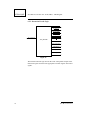
31
0
Descriptor
#0
Control Word
Data Buffer Pointer
#n
Control Word
Data Buffer Pointer
Control Word
Data Buffer Pointer
Control Word
Data Buffer Pointer
Control Word
Data Buffer Pointer
Packet #1
#n+1
Packet #2
#n+2
#n+3
Packet #3
Last Descriptor
31
30
29
OWN SOP EOP
Control Word
Data Buffer Pointer
28 27
20 19
14 13
CHK
SM Checksum_Stuff_Offse Checksum_Start_Offse
Enable
0
Tx_Data_Buffer_Size
Tx_Data_Buffer_Pointer
Figure 10. Transmit Host Data Structures
Sun Microsystems,
41
STP2002QFP
Fast Ethernet, Parallel Port, SCSI (FEPS) - STP2002QFP
5.4.4 Receive Data Structures
Table 12: Receive Data Structures Descriptor Layout: Status Word
Field
Bits
Description
TCP checksum
15:0
This field contains the 16-bit TCP checksum
that was calculated on the entire frame. It will
be updated for every frame that was received
from the network. The software has the choice
of either making use of it or ignoring it.
Free_buffer/Packet_data size
29:16
When the descriptor ownership is passed from
the software to the hardware, this field contains the size of the free buffer that was
allocated for the packet. When the descriptor
ownership is passed from the hardware to the
software, this field indicates the actual number
of packet data bytes that were dumped into the
buffer.
Overflow
30
When an Rx_Buffer_Overflow condition
occurs, this bit will be set to 1 for the frame
that could not fit into the allocated buffer.
Ownership semaphore
31
To turn over ownership, the hardware clears
this bit and the software sets it.
End of packet
29
When set to 1, indicates the last descriptor of
a transmit packet.
Start of packet
30
When set to 1, indicates the first descriptor of
a transmit packet.
Ownership semaphore
31
To turn over ownership, the hardware clears
this bit and the software sets it.
Table 13: Receive Data Structures: Descriptor Layout: Free Buffer Pointer
Field
Free buffer pointer
Bits
Description
31:2
This 29-bit pointer, points to the beginning of the free
buffer. The first byte of the actual packet data inside the
buffer will always reside at a programmable offset from
this location, but within a double-word range.
Programming Restrictions:
• Free receive data buffers must be 64-byte aligned.
42
Sun Microelectronics
Fast Ethernet, Parallel Port, SCSI (FEPS) - STP2002QFP
STP2002QFP
5.4.5 Local Memory Data Structures
The local memory data structures are organized as wrap-around FIFOs that
can store an unlimited number of packets. The transmit and receive data
structures are very similar, except for the format of the control/status word
that is appended to the end of a packet and the alignment of the first byte of a
packet when it is loaded into the FIFO. Also, the RxFIFO does not have a
shadow read pointer. The logical organization of the FIFOs changes depending on the SBus configuration. For a 32-bit SBus, the FIFO organization is
512 words × 33 bits. For a 64-bit SBus, the FIFOs are organized as 256 words
× 65 bits. The 512 words × 33 bits configuration makes use of both the Tag_0
and the Tag_1 bits in the FIFO, while the 256 words × 65 bits configuration
uses only the Tag_0 bit.
On the diagrams shown below, frames #1 and #2 represent a 512 words ×
33 bits configuration, and frame #n represents a 256 words × 65 bits configuration. In reality, of course, only one configuration is used at a given time.
The configuration is selected by programming the extended transfer mode bit
in global configuration register. The amount of “junk” at the beginning of a
frame in the RxFIFO is determined by the first_byte_offset field in the ERX
configuration register.
Sun Microsystems,
43
STP2002QFP
Fast Ethernet, Parallel Port, SCSI (FEPS) - STP2002QFP
0
31
Packet #1
Packet #2
Packet #n
Descriptor
#0
Descriptor
#1
Status Word
Free Buffer Pointer
Status Word
Free Buffer Pointer
Descriptor
#n
Status Word
Free Buffer Pointer
Last Descriptor
Status Word
Free Buffer Pointer
31 30 29
OWN
1
16 15
OverFlow Free_Buffer/Packet_Data Size
0
TCP_Checksum
Free Buffer Pointer
Reserved
Figure 11. Receive Host Data Structure
The software has the capability to read and write the FIFOs (including
tags) at any time, using programmed I/O instructions. This feature should be
used for diagnostic purposes only. During normal operation, the FIFOs are
invisible to the software.
5.4.6 TxFIFO Data Structures
Table 14: TxFIFO Data Structures: Control Word Layout
Field
Last byte boundary
44
Bits
Description
2:0
This field indicates the offset of the last byte of the packet
within the last data word (or double word), depending on the
configuration, in the FIFO
Sun Microelectronics
Fast Ethernet, Parallel Port, SCSI (FEPS) - STP2002QFP
STP2002QFP
Figure 12 below shows the organization of the TxFIFO. The first byte of
the frame is always loaded to be word or double-word aligned.
5.4.7 RxFIFO Data Structures
Table 15: RxFIFO Data Structures: Status Word Layout
Field
Bits
Description
Frame checksum
15:0
This field contains the 16-bit TCP checksum for the
frame, as computed during the frame transfer from the
Rx_MAC to the RxFIFO.
Frame size
26:16
This field indicates the size of the frame in bytes as calculated by the Rx_MAC
Receive abort
30
Reserved
31
This bit communicates the occurrence of a late abort
event to the unload control state machine. The frame
should be dropped and the descriptor reused for the next
frame.
Figure 13 below shows the organization of the RxFIFO. The first byte of
the frame is always loaded at a programmable offset within the first word or
double word.
Sun Microsystems,
45
STP2002QFP
Fast Ethernet, Parallel Port, SCSI (FEPS) - STP2002QFP
Tag_0
Tag_1
63
32 31
0
0
.
.
.
.
Frame #1 Data
.
.
Frame #1 Data
.
.
0
0
Shadow
0
0
Read_Ptr 1
junk
1
Frame #1 Control
0
0
.
.
.
.
Frame #2 Data
Frame #2 Data
Read_Ptr .
.
.
.
0
0
junk
1
0
Frame #2 Control
0
1
.
0
Frame #3 Data
Frame #3 Data
.
.
.
.
.
.
.
.
.
.
.
.
.
.
.
.
.
.
Shadow
Write_Ptr
x
0
x
.
Frame #n Data
x
.
Frame #n Data
x
.
x
0
x
Write_Ptr 0
junk
junk
x
1
Frame #n Control
Frame
#n
Control
x
1
Addr_0
0
32-Bit
Mode
WrapAround
FIFO
64-Bit
Mode
Addr 255
Tag_0/Tag_1
1
2
Reserved
0
Byte
Frame Control
Boundary Word
Figure 12. TxFIFO Organization
5.4.8 Other User Accessible Resources
Besides the host and local memory data structures, the hardware provides a
programmed I/O path to a variety of hardware resources for initialization, error recovery, diagnostics, and network management. From the software perspective, all the programmable resources should be treated as 32-bit entities.
If not all 32 bits are used in a register, the unused bits are grouped as the most
significant bits of the word. Register fields that are not used are ignored during a PIO write, and return 0s during a PIO read. The description of these resources is grouped by functionality and not necessarily by their physical
location. The default value for all the registers/counters is 0x00000000, un-
46
Sun Microelectronics
Fast Ethernet, Parallel Port, SCSI (FEPS) - STP2002QFP
STP2002QFP
less specified otherwise.
Tag_0
Tag_1
63
32 31
0 junk
0
.
.
.
.
Frame #1 Data
.
.
Frame #1 Data
.
.
0
0
0
0
junk
1
1
Frame #1 Control
0
0 junk
.
.
.
.
Frame #2 Data
Frame
#2
Data
Read_Ptr .
.
.
.
0
0
junk
1
0
Frame #2 Control
0
1
.
0 junk
.
.
Frame #3 Data
Frame #3 Data
.
.
.
.
.
.
.
.
.
.
.
.
.
.
.
.
Shadow
Write_Ptr
x
0 junk
x
.
Frame #n Data
x
.
Frame #n Data
x
.
x
0
x
Write_Ptr 0
junk
junk
x
1
Frame #n Control
Frame #n Control
x
1
Addr_0
0
32-Bit
Mode
WrapAround
FIFO
64-Bit
Mode
Addr 255
Tag_0/Tag_1 31
Rx_
30
1 Abort Rsrvd
29
16 15
Frame Size
0
Frame Checksum
Frame Status
Word
Figure 13. RxFIFO Organization
Sun Microsystems,
47
STP2002QFP
Fast Ethernet, Parallel Port, SCSI (FEPS) - STP2002QFP
TESTABILITY
6
6.1 Introduction
This section describes the features of the JTAG Test Access Port (TAP) and
other testability structures for the FEPS. The JTAG macro which implements
the IEEE Standard 1149.1-1990 provides access to the test structures on the
chip.
The TAP includes the TAP controller state machine, an instruction register, a bypass register, a device identification register, and the necessary
decoding logic. The TAP requires five dedicated pads: test data input (TDI),
test data output (TDO), test mode select (TMS), test clock (TCK), and test
reset (TRST).
6.2 JTAG Macro
ISCAN_MODE
JTAG_TDO_EN
JTAG_TCK
BSCAN_CDR
BSCAN_SDI
JTAG_TMS
BSCAN_SDR
BSCAN_UDR
JTAG_TDI
JTAG_CONTR
BSCAN_IMC
BSCAN_OMC
JTAG_TRST
JTAG_TDO
ISCAN_CLK
BSCAN_TDO
ISCAN_SDR
SCSI_SELECT
ISCAN_SO
ISCAN_SDI
Figure 14.
48
Sun Microelectronics
Fast Ethernet, Parallel Port, SCSI (FEPS) - STP2002QFP
STP2002QFP
Table 16: JTAG Macro I/O Signals
JTAG_TCK
JTAG clock from chip pads
JTAG_TDI
JTAG test data in from chip pads
JTAG_TDO
JTAG test data out to chip pads
JTAG_TRST
JTAG test reset from chip pads
JTAG_TMS
JTAG mode select from chip pads
JTAG_TDO_EN
JTAG test data out enable to chip pads
BSCAN_CDR
Boundary scan clock data register
BSCAN_SDI
Boundary scan data input (to BSCAN cells)
BSCAN SDR
Boundary scan shift data register
BSCAN_UDR
Boundary scan update data register
BSCAN_IMC
Boundary scan input mode control
BSCAN_OMC
Boundary scan output mode control
BSCAN_TDO
Boundary scan test data output
ISCAN_CLK
Internal scan clock
ISCAN_SDR
Internal shift select
ISCAN_SDI
Internal scan data input
ISCAN_TDO
Internal scan test data output
SCSI_SELECT
SCSI test mode select signal
ISCAN_MODE
Internal scan mode select signal
The above signals describe the I/O signals of the JTAG macro. The JTAG
macro is composed of the following blocks: TAP controller, instruction register, instruction decode logic, bypass register, internal register clocking
logic, JTAG ID register, JTAG boundary scan control logic, and the TDO
MUX logic.
The following sections describe each of these blocks.
6.2.1 TAP Controller
The TAP controller is a 16-state finite state machine. Transitions between
states occur synchronously at the rising edge of JTAG_TCK in response to
the JTAG_TMS signal or when JTAG_TRST goes low.
Sun Microsystems,
49
STP2002QFP
Fast Ethernet, Parallel Port, SCSI (FEPS) - STP2002QFP
DR_CLOCK
DR_UPDATE
JTAG_TCK
DR_SHIFT
IR_CLOCK
IR_SHIFT
JTAG_TMS
JTAG_TAP
JTAG_TDO_EN
REG_SEL
TAP_RESET
DR_CAPTURE
JTAG_TRST
IR_UPDATE
Figure 15.
6.2.2 Instruction Register
The instruction register is used to select the test to be performed and/or the
test data register to be accessed. The FEPS instruction register is four bits
wide and is a shift register with parallel load and parallel outputs. At the start
of an instruction register shift cycle (during the CAPTURE-IR state), the least
two significant bits are loaded with 01 pattern. During the TEST-LOGIC-RESET controller state the instruction register must have the IDCODE. The instruction register state is updated at the falling edge of the JTAG_TCK. The
shifting of the instruction register occurs at each rising edge of JTAG_TCK.
IR-CLOCK
IR_TDO
IR_SHIFT
JTAG_TDI
JTAG_JR
IR_UPDATE
TAP_RESET
50
IR_VALUE[3:0]
Sun Microelectronics
Fast Ethernet, Parallel Port, SCSI (FEPS) - STP2002QFP
STP2002QFP
Figure 16.
The following instructions are supported in the FEPS.
Table 17: FEPS-Supported Instructions
Value
IMC
OMC
BCAP
ICAP
0000
Extest
Instruction
Boundary
Scan Chain
0
1
1
0
0001
Sample
Boundary
0
0
1
0
0010
Intscan
Internal
0
0
0
1
0011
ATPG
ATPG
1
1
1
1
0100
Debug
Internal
1
1
0
0
0101
Reserved
Bypass
0
0
0
0
0110
Clamp
Bypass
1
1
0
0
0111
Intest
Boundary
1
1
1
0
1000
Reserved
Bypass
0
0
0
0
1001
SCSI_TEST
Bypass
0
0
0
0
1010
Reserved
Bypass
0
0
0
0
1011
Reserved
Bypass
0
0
0
0
1100
SEL_CCR
CCR
0
0
0
0
1101
Reserved
Bypass
0
0
0
0
1110
IDCODE
ID
0
0
0
0
1111
Bypass
Bypass
0
0
0
0
• IMC1 = core driven by boundary scan (BS) cell, 0 = core driven by pin
• OMC1 = pin driven by BS cell, 0 = pin driven by core
• BCAP1 = capture clock generated for BS cell, 0 = no clock
• ICAP1 = capture clock generated for internal flops, 0 = no clock
Sun Microsystems,
51
STP2002QFP
Fast Ethernet, Parallel Port, SCSI (FEPS) - STP2002QFP
6.2.3 Instruction Decode Logic
BYPASS_SELECT
ID_SELECT
ISCAN_MODE
ATPG_SELECT
IR_VALUE[3:0]
INTERNAL_SELEC
T
JTAG_DECODE
DEBUG_SELECT
BSCAN_SELECT
SCSI_SELECT
CCR_SELECT
BSCAN_OMC
Figure 17.
The instruction decode logic decodes the value at the parallel outputs of the
instruction register and selects the appropriate scan data register and control
signals.
52
Sun Microelectronics
Fast Ethernet, Parallel Port, SCSI (FEPS) - STP2002QFP
TDI
STP2002QFP
MUX
ATPG_MODE
BSCAN_CDR
Boundary Scan Register
ISCAN_CLK
Internal Scan Register
IR_CLOCK
JTAG Instruction Register
MUX
DR_CLOCK
JTAG ID Register
DR_CLOCK
Bypass Register
DR_CLOCK
Clock Control Register
Test Mode Selects
Figure 18.
6.2.4 Bypass Register
The bypass register provides a minimum length path between the test data input and the test data output. It consists of a single shift-register stage that
loads a constant 0 in the Capture-DR TAP controller state when the mandatory BYPASS instruction is selected.
JTAG_TDI
DR_CLOCK
DR_SHIFT
JTAG_BYPASS
BYPASS_TDO
BYPASS_SELEC
T
Figure 19.
Sun Microsystems,
53
STP2002QFP
Fast Ethernet, Parallel Port, SCSI (FEPS) - STP2002QFP
6.2.5 Internal Register Clocking Logic
This module generates the scan clock for the internal scan flops and the scan
enable to for the scan flops.
ISCAN_MODE
ISCAN_DR
DEBUG_SELEC
T
IS_CLOCK
DR_CLOCK
DR_CAPTURE
ISCAN_CLK
DR_SHIFT
Figure 20.
6.2.6 JTAG ID Register
This is a 32-bit shift register which has four fields. The least significant bit is
a 1, the next 11 bits [11:1] are the manufacturer’s ID, the next 16 bits [27:12]
are the chip ID, and the most significant 4 bits [31:28] are the chip vintage.
The JTAG ID for FEPS Rev 1.0 is 01792045 hex, for FEPS Rev 2.0 and 2.1
it is 11792045 hex, and for FEPS Rev 2.2 it is 21792045 hex.
JTAG_TDI
DR_CLOCK
JTAG_ID
ID_TDO
DR_SHIFT
ID_SELECT
Figure 21.
6.2.7 Boundary Scan Control Logic
This block generates the boundary scan clock and the boundary scan shift and
update signals which form part of the boundary scan control bus that runs
along the boundary scan chain. This control bus feeds the boundary scan
cells.
54
Sun Microelectronics
Fast Ethernet, Parallel Port, SCSI (FEPS) - STP2002QFP
DR_CLOCK
STP2002QFP
BSCAN_CDR
DR_UPDATE
JTAG_BS
DR_SHIFT
BSCAN_SELECT
BSCAN_UDR
BSCAN_SDR
Figure 22.
6.2.8 TDO MUX logic
This block implements the muxing of the signal which is to appear at the TDO
output pin. It has one flop to ensure that changes on the TDO pin happen on
the falling edge of JTAG_TCK when the data is not being shifted in the data
registers. When data is not being shifted through the chip, TDO is set to a
high-impedance state.
BYPASS_TDO
ISCAN_TDO
BSCAN_TDO
ID_TDO
JTAG_TDO
IR_TDO
CCR_TDO
BYPASS_SELECT
JTAG_TDO_M
CCR_SELECT
ID_SELECT
BSCAN_SDI
ATPG_SELECT
ISCAN_MODE
REG_SEL
JTAG_TCK
BSCAN_SELECT
JTAG_TDI
Sun Microsystems,
55
STP2002QFP
Fast Ethernet, Parallel Port, SCSI (FEPS) - STP2002QFP
Figure 23.
6.3 Special JTAG Instructions
In addition to the mandatory instructions, the FEPS JTAG implements some
special instructions.
6.3.1 Debug Modes
6.3.1.1 Dumping Internal State
Using the DEBUG instruction, the internal chain can be selected. This instruction provides nondestructive internal node visibility during lab debug.
No capture clock is issued for this instruction. While the debug instruction is
selected, both the inputs and outputs are defined by the contents of the boundary scan register.
6.3.1.2 Clock Controller
The clock controller will deterministically stop FEPS internal clocks upon the
occurrence of an external event. The clock controller can only be accessed via
the CCR scan chain. This chain is selected via the SEL_CCR instruction.
The clock controller consists of a stop enable bit and three synchronizers
for the SBus, ENET-Tx, and ENET-Rx domains. When the stop bit is set, the
clock_stop signal will switch the source of the internal clock from the clock
pins to the internal controller. This clock source switching is synchronized to
the rising edge for each clock domain.
6.3.2 INTEST
INTEST can be used to apply stimulus to test the on-chip logic when the chip
sits on a board. This requires that the core be driven off the input boundaryscan cells and the core drives the output boundary-scan cells. For this we require that the clock pads be made controllable via boundary scan. INTEST
can also be used to apply burn-in vectors if the burn-in tester is pin limited
and can’t accommodate all the FEPS pins.
6.3.3 SCSI Test Mode
The SCSI Test mode will provide access to the I/O signals of the SCSI
FAS366 core through the I/O pins. This mode isolates the SCSI core by providing controllability and observability to its I/O signals. The vectors applied
will yield 95% coverage in the SCSI core area which does not have internal
scan.
56
Sun Microelectronics
Fast Ethernet, Parallel Port, SCSI (FEPS) - STP2002QFP
STP2002QFP
6.4 Clock Stop Pin
This pin can deterministically stop the clocks in FEPS. After the instruction
register is updated with the SEL_CCR instruction, an initializing pattern is
loaded into the CCR scan data register. In the run-test/idle state, any external
event which triggers the clock stop pin will switch the clock source from the
clock pins to the ISCAN_CLK signal generated by the JTAG logic. This signal is held high in the run-test/idle controller state. The switching is synchronized with the rising edge of the clocks of the respective clock domains.
The clocks that need to be stopped are those that are those that control the
flops in the full scan area which are the SBus, ENET-Tx, and ENET-Rx
clocks.
Int_Scan_Enable shifts the clock between the SBus_CLK and the
ISCAN_CLK. This clock tree feeds the scan flops in the SBA, parallel port,
and SCSI DMA where the scan flops have the same system and scan clock.
ENET_Tx_Scan_En is the clock enable for the scan flops in the Ethernet
Tx clock domain. Here the scan flops have TX_CLK as the system clock and
a SBUS_CLK as the scan clock. ENET_Rx_Scan_En is the clock enable for
the scan flops in the Ethernet Rx clock domain. Here the scan flops have
RX_CLK as the system clock and a SBUS_CLK as the scan clock.
6.5 Test Vectors
The RAMs and data buffers are tested using high-coverage functional vectors
which target memory-specific faults. The full scan area is tested by combinational ATPG vectors which yield a high fault coverage.
Sun Microsystems,
57
STP2002QFP
Fast Ethernet, Parallel Port, SCSI (FEPS) - STP2002QFP
PROGRAMMING MODEL
7
7.1 Introduction
Refer to the FEPS application note (STB0106) for programming notes and a
complete address map for the registers for all interfaces.
7.2 Parallel Port Channel Registers
7.2.1 Control/Status Register
Table 18: Control/Status Register Address
Register
Control/Status register (P_CSR)
Physical Address
Access Size
0xC80_0000
4 bytes
Table 19: Control/Status Register Definition
Field
P_INT_PEND
Bits
Description
Type
0
Set when a PP DMA or PP control interrupt is pending or when P_TC is set
and P_TCI_DIS is not set.
R
P_ERR_PEND
1
Set when an interrupt is pending due to an SBus error condition.
R
P_DRAINING
3:2
Both bits set when the P_FIFO is draining to memory, otherwise both bits are
0.
R
P_INT_EN
4
When set, enables SB_P_IRQ to become active when either P_INT_PEND or
P_ERR_PEND is set.
R/W
P_INVALIDATE
5
When set, invalidates the P_FIFO. Resets itself. Reads as 0.
P_SLAVE_ERR
6
Set on slave access size error to a PP register. Reset by P_RESET,
P_INVALIDATE, or writing to 1.
R/W
P_RESET
7
When set, acts as a hardware reset to the parallel port only.
R/W
P_WRITE
8
DMA direction. 1 = to memory; 0 = from memory
R
9
When set, enables DMA transfers to/from the PP.
R/W
P_EN_DMA
W
12:10
P_EN_CNT
13
When set, enables the PP byte counter to be decremented
R/W
P_TC
14
Terminal count. Set when byte count expires. Reset on write of 1 if
P_EN_NEXT=1.
R/W
REV_MIN [2:0]
17:15
FEPS minor revision number
P_BURST_SIZE
19:18
Defines sizes of SBus read and write bursts for PP transfers.
R/W
When set, disables draining and resetting of P_FIFO on loading of P_ADDR
register.
R/W
P_DIAG
20
22:21
58
Sun Microelectronics
Fast Ethernet, Parallel Port, SCSI (FEPS) - STP2002QFP
STP2002QFP
Table 19: Control/Status Register Definition
Field
Bits
Description
Type
P_TCI_DIS
23
When set, disables P_TC from generating an interrupt.
R/W
P_EN_NEXT
24
When set, enables DMA chaining and next address/byte count auto-load
mechanism. P_EN_CNT must also be set.
R/W
P_DMA_ON
25
DMA On. When set, indicates that DMA transfers are not disabled due to any
hardware or software condition.
R
P_A_LOADED
26
Set when the contents of the address and byte count are considered valid during chained transfers.
R
P_NA_LOADED
27
Set when next address and byte count registers have been written but have not
been used for chaining.
R
REV_MAJ [3:0]
31:28
FEPS major revision number
R
The RESET state of this register is as follows:
P_ERR_PEND = 0
P_INVALIDATE = 0
P_RESET = 0
P_EN_CNT = 0
P_BURST_SIZE = 0
P_EN_NEXT = 0
P_A_LOADED = 0
P_WRITE = 1
P_INT_EN = 0
P_SLAVE_ERR = 0
P_EN_DMA = 0
P_TC = 0
P_TCI_DIS = 0
P_DMA_ON = 0
P_NA_LOADED = 0
P_INT_PEND:
Interrupt pending is the logical OR of the following enabled PP interrupt
sources:
(P_TC and !P_TCI_DIS), DS_IRQ, ACK_IRQ, BUSY_IRQ, ERR_IRQ,
PE_IRQ, SLCT_IRQ.
P_ERR_PEND:
Error pending will be set due to an SBus error acknowledge or an SBus late
error. It indicates an SBus error condition. PP DMA is stopped
(P_DMA_ON=0) when this bit is set. This bit can be reset by setting
P_INVALIDATE or P_RESET.
P_DRAINING:
When P_FIFO is draining to memory, both bits are set. Do not assert
P_RESET or P_INVALIDATE or write to the P_ADDR register when set.
Sun Microsystems,
59
STP2002QFP
Fast Ethernet, Parallel Port, SCSI (FEPS) - STP2002QFP
P_DRAINING bits are not valid while P_ERR_PEND is set and should be ignored.
P_INVALIDATE:
Setting this bit invalidates the P_FIFO. If P_ERR_PEND = 0 when
P_INVALIDATE is set, all dirty data in the P_FIFO will first be drained to
memory. If P_ERR_PEND = 1 when P_INVALIDATE is set, all dirty data
in the P_FIFO will be discarded. In addition to invalidating the P_FIFO, setting this bit causes P_ERR_PEND and P_TC to be reset. If P_EN_NEXT =
1, P_A_LOADED, and P_NA_LOADED will also be reset.
P_RESET:
This bit functions as a hardware reset to the parallel port. It will remain active
once written to one until written to zero, unless cleared by an SBus reset
(SB_RESET asserted). Setting P_RESET or asserting SB_RESET will invalidate the P_FIFO and reset all parallel port interface state machines to their
idle states. If P_ERR_PEND = 0 when P_RESET is set, all dirty data in the
P_FIFO will first be drained to memory. When this occurs, P_RESET must
not be cleared until draining is complete, as indicated by P_DRAINING = 00.
If P_ERR_PEND = 1 when P_RESET is set, no draining will take place and
all dirty data in the P_FIFO will be discarded.
P_WRITE:
This read only bit reflects the direction for DMA transfers. It is a logical OR
of the DIR bit of the parallel control register (P_TCR) and the MEM_CLR bit
of the parallel operation control register (P_OCR).
P_EN_DMA:
When set, enables DMA transfer to/from parallel port. Loss of data may occur
when DMA is disabled in the middle of a data transfer from parallel port.
P_TC:
This bit will be set when the byte counter (P_BCNT) transitions to/from
0x000001 to 0x000000. This will generate an interrupt if enabled by
P_INT_EN and not disabled by P_TCI_DIS. During unchained transfers,
P_TC causes P_DMA_ON to be reset. When P_EN_NEXT = 0, P_TC is
cleared by P_INVALIDATE, P_RESET, or SB_RESET. When
P_EN_NEXT = 1, P_TC can also be cleared by writing a 1 to it.
60
Sun Microelectronics
Fast Ethernet, Parallel Port, SCSI (FEPS) - STP2002QFP
STP2002QFP
P_BURST_SIZE:
This field defines the sizes of SBus read and write bursts used by the FEPS
for parallel port transfers. All reads from memory will be one size, either 4,
8, or 1 word (in “no burst mode). SBus writes to memory can be byte, halfword, or one of the burst sizes given in the table. The FEPS will always use
the largest possible size for writes, which is dependent on P_BURST_SIZE
and the number of bytes that need to be drained. Also, P_BURST_SIZE determines the draining level of the P_FIFO. When the P_FIFO has been filled
with this amount of data, it will always be drained to memory. The sizes given
in Table 20 are in SBus words.
Table 20:
P_BURST_SIZ
E
1SBus
RD_BURST_SIZ
E
WR_BURST_SIZES
FIFO_Draining_Level
00
4 words
4 words
4 words
01
8 words
4, 8 words
8 words
No bursts
1 word
Reserved
Reserved
bursts1
10
No
11
Reserved
reads are always one word in no burst mode.
P_DMA_ON:
When set, indicates that the FEPS is able to respond to parallel port DMA requests. Reads as 1 when (P_A_LOADED or P_NA_LOADED) and
P_EN_DMA & !(P_ERR_PEND); otherwise reads as 0.
REV_MIN [2:0]:
FEPS minor revision number.
REV_MAJ [3:0]:
FEPS major revision number. Starts from 2.
Example: for Rev x.y silicon, the {REV_MAJ[3:0], REV_MIN[2:0] = [x,y]}
Sun Microsystems,
61
STP2002QFP
Fast Ethernet, Parallel Port, SCSI (FEPS) - STP2002QFP
7.2.2 DMA Address and Next Address Register
Table 21: DMA Address and Next Address Register Address
Register
Physical Address
Access Size
0xC80_0004
4 bytes
DMA address and next address register (P_ADDR)
Table 22: DMA Address and Next Address Register Definition
Field
Bits
Description
P_ADDR
31:0
DVMA address register
P_NEXT_ADDR
31:0
Next DVMA address register
Type
R/W
W
This 32-bit read/write register contains the virtual address for parallel port
DMA transfers. It is implemented as a 32-bit loadable counter which points
to the next byte that will be accessed via the parallel port.
If the P_EN_NEXT (enable next address) bit in the P_CSR is set, then a
write to the P_ADDR register will write to the P_NEXT_ADDR register
instead. If P_EN_NEXT is set when the byte counter (P_BCNT) expires, and
the P_NEXT_ADDR register has been written since the last time the byte
counter expired, then the contents of P_NEXT_ADDR are copied into
P_ADDR. If P_EN_NEXT is set when the byte counter (P_BCNT) expires,
but the P_NEXT_ADDR register has not been written since the last time the
byte counter expired, then DMA activity is stopped and DMA requests from
the parallel port will be ignored until P_NEXT_ADDR is written or
P_EN_NEXT is cleared. (Also, the P_DMA_ON bit will read as 0 while
DMA is stopped because of this.) When DMA is re-enabled by writing to the
P_NEXT_ADDR register, the contents of P_NEXT_ADDR are copied into
P_ADDR before DMA activity actually begins.
Note: A write to the P_ADDR register will invalidate the P_FIFO. A
write to the P_NEXT_ADDR register does not have this effect.
62
Sun Microelectronics
Fast Ethernet, Parallel Port, SCSI (FEPS) - STP2002QFP
STP2002QFP
7.2.3 Byte Count Register
Table 23: Byte Count Register Address
Register
Byte count register (P_BCNT)
Physical Address
Access Size
0xC80_0008
4 bytes
Table 24: Byte Count Register Definition
Field
Bits
Description
P_BCNT
23:0
DMA byte count register
P_NEXT_BCNT
23:0
Next DMA byte count register
Type
R/W
W
This register is implemented as a 24-bit down counter. When reading this register as a word, bits 31:24 will read as 0s. The register should be loaded with
a 24-bit byte count which, if enabled via the P_EN_CNT bit in the P_CSR,
will be decremented every time a byte is transferred between the FEPS and
whatever external device is connected to the parallel port. During a transition
of this register from 1 to 0, the terminal count signal (P_TC), will generate an
interrupt if not disabled via the P_TCI_DIS bit of the P_CSR.
If the P_EN_NEXT bit in the P_CSR is set, then a write to the P_BCNT
register will write to the P_NEXT_BCNT register instead. Whenever the
P_NEXT_ADDR register is copied into the P_ADDR register, the
P_NEXT_BCNT register is copied into the P_BCNT register at the same
time. If P_NEXT_ADDR is being copied in P_ADDR and P_NEXT_BCNT
has not been written since the last time P_NEXT_BCNT was copied in
P_BCNT, the last value that was written into P_NEXT_BCNT will again be
copied into P_BCNT. This provides a shortcut in setting up consecutive
DMA transfers of equal size from different addresses, in that
P_NEXT_BCNT only needs to be written once as long as P_NEXT_ADDR
is loaded for each successive transfer. If P_EN_NEXT is not set when
P_BCNT expires (changes from 0x000001 to 0x000000), then parallel port
DMA activity will be stopped and the P_DMA_ON bit will read as 0 until
P_ADDR is written. If P_EN_NEXT is set, then DMA will be stopped on
P_BCNT expiration.
Note: Loading P_BCNT with 0 will allow 2**24 bytes to be transferred before it expires.
Sun Microsystems,
63
STP2002QFP
Fast Ethernet, Parallel Port, SCSI (FEPS) - STP2002QFP
7.2.4 Test Control/Status Register
Table 25: Test Control/Status Register Address
64
Register
Physical Address
Access Size
Test control/Status register (P_TST_CSR)
0xC80_000C
4 bytes
Sun Microelectronics
Fast Ethernet, Parallel Port, SCSI (FEPS) - STP2002QFP
STP2002QFP
Table 26: Test Control/Status Register Definition
Bits
Description
Type
LD_TAG
Field
31
When set to 1. loads FIFO DMA address register
(ADDR_TAG) with value in D_ADDR
W
REQ_OUT
30
Reads as 1, when FIFO is making a request for an
SBus read or write.
R
RD_BURST
30
When set to 1, initiates a DMA burst read from
memory into FIFO from address in ADDR_TAG
W
WR_CNT
29
When set to 1, loads FIFO_CNT register with
D_TST_CSR[5:0]
W
WRITE
28
When set to 1, puts FIFO into WRITING mode.
Reads as 1 when FIFO in WRITING mode.
R/W
DRAIN
27
Reads as 1 if FIFO is draining. When set to 1,
forces FIFO to drain.
R/W
EMPTY
26
Reads as 1, if FIFO buffer empty.
FULL
25
Reads as 1, if FIFO buffer is full.
R
LO_MARK
24
Reads as 1, if FIFO buffer has enough room for 1
SBus read burst of data.
R
HI_MARK
23
Reads as 1, if FIFO contains enough data for 1
SBus write burst.
R
COUNT
5:0
Reads CNT register containing number of bytes
stored in FIFO buffer.
R
COUNT
5:0
When WR_CNT=1, write CNT register containing number of bytes stored in FIFO buffer.
W
R
Note:The P_TST_CSR is intended for diagnostic and test use only and should never be
written while a DMA transfer is active
7.2.5 Hardware Configuration Register
Table 27: Hardware Configuration Register Address
Register
Hardware configuration register (P_HCR)
Sun Microsystems,
Physical Address
Access Size
0xC80_0010
2 bytes
65
STP2002QFP
Fast Ethernet, Parallel Port, SCSI (FEPS) - STP2002QFP
Table 28: Hardware Configuration Register Definition
Bits
Description
Type
DSS
Field
6:0
Data setup before data strobe in increments of 1 SBus clock
R/W
DSW
14:8
TEST
15
7
Unused. Reads as 0
R
Data strobe width in increments of 1 SBus clock
R/W
Test bit which when set, allows the buried counters to be
read
R/W
DSS:
Data setup to data strobe. This 7-bit quantity is used to define several different timing specifications for the interface. The contents of this field of the register are used to load a hardware timer whose timebase is the SBus clock. The
programmability range is from a minimum of 0 SBus clocks to 127 SBus
clocks. Bit 0 is the LSB and bit 6 is the MSB. The sections on unidirectional
and bidirectional transfers should be referenced for detail information on the
use of this timer.
DSW:
Data strobe width. This 7-bit quantity is used to define data strobe and acknowledge pulse widths for the interface. The contents of this field of the register are used to load a hardware timer whose timebase is the SBus clock. The
programmability range is from a minimum of 3 SBus clocks to 127 SBus
clocks. In the case of the value being 0, 1, 2, or 3, the timer will be loaded
with a value of 3. Bit 8 is the LSB and bit 14 is the MSB. The sections on unidirectional and bidirectional transfers should be referenced for detail information on the use of this timer.
7.2.6 Operation Configuration Register
This 16-bit read/write register is used to specify the operation of the interface.
Bidirectional specification of the control signals (P_D_STRB, P_ACK,
P_BSY), handshake protocol, memory clear, and diagnostic mode are defined
in this register. The detailed function of the bits is described in Table 30. Reset value of this register is all bits 0, except DS_DSEL and IDLE, which are
reset to 1, and bit 1, which always reads as 1 for backward compatibility with
the HIOD parallel port.
66
Sun Microelectronics
Fast Ethernet, Parallel Port, SCSI (FEPS) - STP2002QFP
STP2002QFP
Table 29: Operation Configuration Register Address
Register
Operation configuration register (P_HCR)
Physical Address
Access Size
0xC80_0012
2 bytes
Table 30: Operation Configuration Register Definition
Field
IDLE
SRST
Bits
Description
Type
0
Reserved
R/W
1
Reserved
R
2
Reserved
R
3
Reads as 1, when the PP data transfer state machines
are idle
R
4
Reserved
R
5
Reserved
R
6
Reserved
R
7
When set, resets the parallel port. Must be reset by
software.
R/W
ACK_OP
8
Acknowledge operation
R/W
BUSY_OP
9
Busy operation
R/W
EN_DIAG
10
When set, enables diagnostic operation
R/W
ACK_DSEL
11
Acknowledge bidirectional select. When set,
P_BSY is bidirectional
R/W
BUSY_DSEL
12
Busy bidirectional select. When set, P_D_STRB is
bidirectional
R/W
DS_SEL
13
Data strobe bidirectional select. When set,
P_D_STRB is bidirectional
R/W
DATA_SRC
14
Data source for memory clear operation
R/W
MEM_CLR
15
When set, enables memory clear
R/W
IDLE:
When this bit is set, it indicates that the parallel port data transfer state machines are in their idle states. The state machines should be idle when changing direction and/or configuring operational modes and when enabling a
memory clear operation.
SRST:
Setting this bit will place the parallel port data transfer state machines and
programmable timers into reset. It will not reset any of the parallel port reg-
Sun Microsystems,
67
STP2002QFP
Fast Ethernet, Parallel Port, SCSI (FEPS) - STP2002QFP
isters. This bit must be reset by software.
ACK_OP:
Used to specify the handshake protocol to be used on the interface. The meaning of this bit differs depending on the direction of transfer. The sections on
unidirectional and bidirectional transfers should be referenced for detail information on this bit. The general definition is as follows:
1 = Handshake using PP_ACK
0 = PP_ACK is inactive
BUSY_OP:
Used to specify the handshake protocol to be used on the interface. The meaning of this bit differs depending on the direction of transfer. The sections on
unidirectional and bidirectional transfers should be referenced for detail information on this bit. The general definition is as follows:
1 = Handshake performed using PP_BSY
0 = PP_BSY is not used for handshaking
EN_DIAG:
Setting this bit enables diagnostic mode which does three things:
• Bits 0–2 of the output register are gated on to bits 0–2 of the input register. This allows testing of the data path and the interrupt generation
logic.
• The internal DS, ACK, and BUSY latch bits drive the internal DS_IRQ
and ACK_IRQ, and BUSY_IRQ interrupt-generation logic.
• When reading the DS, ACK, and BUSY bits of the transfer control register, the read data comes from the internal latches instead of the external pins. During diagnostic mode, if the DS or ACK bits are configured
as outputs, the output pins will be gated to an inactive level. The BUSY
output will be driven active and the DIR output will be latched in its
current state.
ACK_DSEL:
This bit is a bidirectional select for the PP_ACK signal. When this bit is 0,
PP_ACK is an input, when 1 it is a bidirectional signal. The PP_ACKDIR pin
will reflect the direction of PP_ACK. The switching of direction is controlled
by the DIR bit of the transfer control register. The function of the two pins
is as follows:
DIR=0
DIR=1
PP_ACK
Input
Output
68
Sun Microelectronics
Fast Ethernet, Parallel Port, SCSI (FEPS) - STP2002QFP
PP_ACKDIR0
STP2002QFP
1
BUSY_DSEL:
This bit is a bidirectional select for the PP_BSY signal. When reset, PP_BSY
is fixed as an input. When set, PP_BSY is a bidirectional signal. The
PP_BSYDIR pin will reflect the direction of PP_BSY. The switching of direction is controlled by the DIR bit of the transfer control register. The function of the two pins is as follows:
DIR=0
DIR=1
PP_BSY
Input
Output
PP_BSYDIR 0
1
DS_DSEL:
This bit is a bidirectional select for the PP_STB signal. When reset, PP_STB
is fixed as an output. When set, PP_STB is a bidirectional signal. The
PP_DSDIR pin will reflect the direction of PP_STB. The switching of direction is controlled by the DIR bit of the transfer control register. The function
of the two pins is as follows:
DIR=0
DIR=1
PP_STB
Output
Input
PP_DSDIR 1
0
This bit also defines transfer protocol as follows:
1 = Data strobe is bidirectional. Master write transfer protocol is selected.
0 = Data strobe is fixed as an output. Master read/write transfer protocol is
selected.
DATA_SRC:
This bit specifies the data to be sourced during a memory clear operation.
When set, the sourced data will be ones. When reset, the sourced data will be
0s.
MEM_CLR:
This bit enables memory clear operation. The DMA control registers need to
be configured, the DIR bit in the TCR register must be set and DMA must be
enabled.
Sun Microsystems,
69
STP2002QFP
Fast Ethernet, Parallel Port, SCSI (FEPS) - STP2002QFP
7.2.7 Parallel Data Register
The data register is an 8-bit read/write port used to transfer data to and from
the external device. In programmed I/O mode data written to this register is
presented to the I/O pins if the DIR bit of the transfer control register is 0. A
read of this register will result in the data previously written or if the DIR bit
of the transfer control register is set to 1, the latched data from the last data
strobe. The data port is not accessible via slave write cycles during DMA
(P_DMA_ON=1). Any write cycles during DMA will not generate errors, the
data will simply not be written.
Since both DMA and PIO share the same data register, internal loopback
is possible by running a single-byte DMA cycle followed by a PIO cycle to
verify the data. This will test both the DMA and slave data paths.
Table 31: Parallel Data Register Address
Register
Parallel data register (P_DR)
Physical Address
Access Size
0xC80_0014
1 byte
Table 32: Parallel Data Register Definition
Field
P_DR
Bits
7:0
Description
Parallel data
Type
R/W
7.2.8 Transfer Control Register
The transfer control register is an 8-bit register whose contents define/reflect
the state of the external interface handshake and direction control signals. The
DS, ACK, and BUSY bits will reflect the state of the external pins, when read.
Writing these bits defines a value to be driven onto the external pins if the individual direction select bits (DS_DSEL, ACK_DSEL, BUSY_DSEL) and
the direction control bit (DIR) are configured such that the HIOD is driving
these pins as outputs. The write bits and read bits are different. That means
that values typically written to these bits may not be reflected on a read cycle.
However, by setting the EN_DIAG bit of the operation control register, these
register bits become read/write (see the EN_DIAG bit description of the
OCR).
70
Sun Microelectronics
Fast Ethernet, Parallel Port, SCSI (FEPS) - STP2002QFP
STP2002QFP
Table 33: Transfer Control Register Address
Register
Transfer Control register (P_TCR)
Sun Microsystems,
Physical Address
Access Size
0xC80_0015
1 byte
71
STP2002QFP
Fast Ethernet, Parallel Port, SCSI (FEPS) - STP2002QFP
Table 34: Transfer Control Register Definition
Field
DS
Bits
0
Description
Type
Data strobe
R/W
ACK
1
Acknowledge
R/W
BUSY
2
Busy (active low)
R/W
R/W
DIR
3
Direction control. 0 = write to external device, 1 = read
4
Unused (reads as 0)
R
5
Unused (reads as 0)
R
6
Unused (reads as 0)
R
7
Unused (reads as 0)
R
DS:
Reading this bit reflects the state of the bidirectional PP_STB pin. Writing
this bit with DS_DSEL=0 or with DS_SEL=1 and DIR=0 will cause the value
written to be driven onto PP_STB. The reset state of the output latch is 0, but
the value read back from this bit after reset will reflect the input signal being
driven onto PP_STB.
ACK:
Reading this bit reflects the state of the bidirectional PP_ACK pin. Writing
this bit with ACK_DSEL=1 will cause the value written to be driven onto
PP_ACK if DIR=1. The reset state of the output latch is 0, but the value read
back from this bit after reset will reflect the input signal being driven onto
PP_ACK.
BUSY:
Reading this bit reflects the state of the bidirectional PP_BSY pin. Writing
this bit with BUSY_DSEL=1 will cause the value written to be driven onto
PP_BSY if DIR=1. The reset state of the output latch is 0, but the value read
back from this bit after reset will reflect the input signal being driven onto
PP_BSY.
DIR:
This bit defines and controls the direction of data transfer: 0=write to external
device,
1= read from external device. It is also driven externally on the PP_DDIR pin.
This bit also controls the direction of DMA operation. In the case of a memory clear operation, this bit (must be set) and the MEM_CLR bits define the
72
Sun Microelectronics
Fast Ethernet, Parallel Port, SCSI (FEPS) - STP2002QFP
STP2002QFP
DMA direction. The state of the DIR bit is reflected in the P_WRITE bit of
the P_CSR. Reset state of this bit is 1.
7.2.9 Output Register
The output register is an 8-bit read/write register whose contents are driven
on to the corresponding external pins. In diagnostic mode (EN_DIAG=1),
bits 0–2 are gated on to input register bits 0–2. The external outputs remain
low while diagnostic mode is enabled. All bits are 0 after reset.
Table 35: Output Register Address
Register
Output register (P_OR)
Physical Address
Access Size
0xC80_0016
1 byte
Table 36: Output Register Definition
Field
Bits
Description
Type
SLCT_IN
0
Select in. This bit is output on the PP_SLCT_IN pin.
R/W
AFXN
1
Auto feed. This bit is output on the PP_AFXN pin.
R/W
INIT
2
Initialize. This bit is output on the P_INIT pin
R/W
3
Reserved (V1 bit on HIOD parallel port)
R/W
4
Reserved (V2 bit on HIOD parallel port)
R/W
5
Reserved (V3 bit on HIOD parallel port)
R/W
6
Unused (reads as 0)
R
7
Unused (reads as 0)
R
7.2.10 Input Register
The input register is an 8-bit read/write register whose contents reflect the
state of several external input pins and their corresponding interrupts. In diagnostic mode (EN_DIAG=1), bits 0–2 are driven from output register bits
0–2.
Table 37: Input Register Address
Register
Input register (P_IR)
Sun Microsystems,
Physical Address
Access Size
0xC80_0017
1 byte
73
STP2002QFP
Fast Ethernet, Parallel Port, SCSI (FEPS) - STP2002QFP
Table 38: Input Register Definition
Bits
Description
Type
ERR
Field
0
Error input. This pin reflects the state of the ERR input pin
R
SLCT
1
Select input. This pin reflects the state of the SLCT input
pin
R
PE
2
Paper empty. This pin reflects the state of the PP_PE input
pin
R
3
Unused (reads as 0)
R
4
Unused (reads as 0)
R
5
Unused (reads as 0)
R
6
Unused (reads as 0)
R
7
Unused (reads as 0)
R
7.2.11 Interrupt Control Register
This 16-bit read/write register is used to specify operation of the parallel port
interrupts. Interrupt enables, polarity, and IRQ pending bits are contained in
this register. The detailed function of these bits are described following the
table. Reset value of this register is all bits 0.
Table 39: Interrupt Control Register Address
Register
Interrupt Control register (P_ICR)
74
Physical Address
0xC80_0018
Access Size
2 bytes
Sun Microelectronics
Fast Ethernet, Parallel Port, SCSI (FEPS) - STP2002QFP
STP2002QFP
Table 40: Interrupt Control Register Definition
Field
Bits
Description
Type
ERR_IRQ_EN
0
When set, enables ERR interrupts
R/W
ERR_IRP
1
ERR interrupt polarity. 1=on rising edge, 0=on
trailing edge
R/W
SLCT_IRQ_EN
2
When set, enables SLCT interrupts
R/W
SLCT_IRP
3
SLCT interrupt polarity. 1=on rising edge, 0=on
trailing edge
R/W
PE_IRQ_EN
4
When set, enable PE interrupts
R/W
PE_IRP
5
PE interrupt polarity. 1=on rising edge, 0=on
trailing edge
R/W
BUSY_IRQ_EN
6
When set, enables BUSY interrupts
R/W
BUSY_IRP
7
BUSY interrupt polarity. 1=on rising edge, 0=on
trailing edge
R/W
ACK_IRQ_EN
8
When set, enables ACK interrupts on rising edge
of ACK
R/W
DS_IRQ_EN
9
When set, enables DS interrupts on the rising
edge of DS
R/W
ERR_IRQ
10
When set, error IRQ pending
R/W
SLCT_IRQ
11
When set, select IRQ pending
R/W
PE_IRQ
12
When set, paper IRQ pending
R/W
BUSY_IRQ
13
When set, busy IRQ pending
R/W
ACK_IRQ
14
When set, acknowledge IRQ pending
R/W
DS_IRQ
15
When set, data strobe IRQ pending
R/W
*_IRQ_EN: When set, enables interrupts on the corresponding bits of the
input and transfer control registers. Note that the interrupt enable bit of the
PD_SCR must also be enabled to allow a hardware interrupt to be generated.
*_IRP: Defines the polarity of the edge triggered interrupts on the corresponding bits of the input register. 0=interrupt generated on the 1 to 0
transition of the signal. 1= interrupt generated on the 0 to 1 transitions of the
signal. Note that when configuring the interrupt polarity of a given signal, it
is possible to generate a false interrupt. It is suggested that when the interrupt
polarities are being programmed, interrupts be disabled, and all interrupt
sources be cleared upon completion of programming.
ERR_IRQ, SLCT_IRQ, PE_IRQ, BUSY_IRQ:
When set, an interrupt is pending on the corresponding bit. The interrupt is
cleared and the bit is reset when a 1 is written to the corresponding bit. WritSun Microsystems,
75
STP2002QFP
Fast Ethernet, Parallel Port, SCSI (FEPS) - STP2002QFP
ing a 0 to these locations leaves the bit(s) unchanged.
ACK_IRQ:
When set, an interrupt is pending due to the receipt of PP_ACK. The interrupt
is set on the 0 to 1 transition of PP_ACK. This interrupt is intended to facilitate PIO transfers while configured as master under master write protocol.The
interrupt is cleared and the bit is reset when a 1 is written to this bit. Writing
a 0 to this location leaves the bit unchanged.
DS_IRQ:
When set, an interrupt is pending due to the receipt of PP_STB. This interrupt
is intended to facilitate PIO transfers while configured as slave under master
write protocol. The interrupt is cleared and the bit is reset when a 1 is written
to this bit. Writing a 0 to this location leaves the bit unchanged.
7.3 SCSI Channel Registers
7.3.1 SCSI Control/Status Register
Table 41: Control/Status Register Address
Register
Physical Address
Control/Status register (D_CSR)
0x880_0000
Access Size
4 bytes
Table 42: Control/Status Register Definition
Field
Bits
Description
Type
D_INT_PEND
0
Set when either FAS366_IRQ is active, or if
D_ERR_PEND is set, or if DVMA loop-back is
complete
R
D_ERR_PEND
1
Set when a SCSI DVMA transfer received an
SBus ERR acknowledge. Also set when a parity
error or a late error detected
R
D_DRAINING
2
Non-zero when buffers are draining SCSI data to
memory; 0 otherwise
R
3
Reserved
4
When set, enables SBus SCSI_IRQ when
INT_PEND or ERR_PEND is set
5
Reserved (reads as 0)
6
Reserved (reads as 0)
7
When set, invalidates the buffers and resets SCSI
CE
D_INT_EN
D_RESET
76
R
R/W
R
R
R/W
Sun Microelectronics
Fast Ethernet, Parallel Port, SCSI (FEPS) - STP2002QFP
STP2002QFP
Table 42: Control/Status Register Definition
Field
Bits
Description
Type
D_WRITE
8
DMA direction for SCSI transfers; 1 = to memory, 0 = from memory
R/W
D_EN_DMA
9
When set, enables DMA from the FAS366
unless blocked by other conditions
R/W
D_REQ_PEND
10
D_DMA_REV
14:11
D_WIDE_EN
15
When set, enables wide-mode SBus DVMA for
SCSI
16
Reserved (reads as 1)
17
When set, disables drain of buffers on slave
accesses to the FAS366 registers
R/W
Defines SCSI DVMA burst size (see table
below)
R/W
D_DSBL_ESP_DR_
N
D_BURST_SIZE
19:18
Do not assert D_RESET, while this is a 1
R
0001 for current implementation
R
R/W
R
20
Reserved (reads as 1)
21
If set, provides a 2-cycle DMA access to
FAS366, else it is a 3-cycle access. Default value
is 0.
22
Reserved (reads as 0)
R
23
Reserved (reads as 1)
R
24
Reserved (reads as 0)
R
D_DSBL_PARITY_C
HK
25
When set, disables checking for parity on the
bus. Default value is a 1.
R/W
D_PAUSE_FAS366
26
When asserted, it will cause FAS366 pause input
to be asserted. Default value is 0.
R/W
D_HW_RST_FAS366
27
When asserted, it will cause the hardware reset
to FAS366 to be asserted. Default value is 0.
R/W
D_TWO_CYCLE
D_DEV_ID
31:28
R
Device ID (1011 for this implementation)
R/W
R
Table 43: BURST_SIZE Encoding
BURST_SIZ
E
Read Burst Size
Write Burst Size
Buffer Drain Level
00
4 words
4 words
16 words
01
8 words
8 words
16 words
10
Reserved
Reserved
Reserved
11
16 words
16 words
16 words
D_INT_PEND:
Sun Microsystems,
77
STP2002QFP
Fast Ethernet, Parallel Port, SCSI (FEPS) - STP2002QFP
This bit is set to indicate that FAS366 has asserted its interrupt signal. Once
FAS366 asserts its interrupt signal, all the bytes in prefetch buffers are
drained to the host memory, before setting this bit or generating an interrupt
on SBus. Draining of buffers, before posting the interrupt to device driver,
saves PIOs. This bit will also be set during DMA loop-back. This bit will also
be set when the D_ERR_PEND bit is set.
D_ERR_PEND:
This bit is set in response to an Error ACK, during DVMA. This bit is reset
on setting D_RESET. This bit will also be set, when a parity error or a late
error is detected.
D_DRAINING:
When the buffers are draining to memory, this bit is set. DO NOT assert
D_RESET or write to D_ADDR register when set. This bit is not valid while
D_ERR_PEND is set and should be ignored.
D_RESET:
This bit will remain active once set to 1, until set to 0 or is cleared by a hardware reset. Setting D_RESET or asserting hardware reset will invalidate the
prefetch buffers, reset all of the state machines to their idle states.
Note: This bit must be asserted at the end of each DMA transfer. In
other words, whenever D_ADDR and D_BCNT are programmed with
a new value, D_RESET should have been asserted prior to this
programming.
D_REQ_PEND: This bit is set when a DVMA read or write request is pending. Do not assert D_RESET when D_REQ_PEND or/and D_DRAINING
bit(s) is (are) set.
D_DSBL_ESP_DRN: If set, draining will not be forced when the CPU
makes a slave access to the FAS366, while SCSI DVMA is in progress. This
bit could be useful in block-mode operation, where FAS366 does not generate
interrupts on successful execution of commands. In such a case, device drivers can use this bit to prevent forced draining, when making a slave access to
the FAS366 to monitor status.
7.3.2 SCSI Address Register
This register indicates the starting address from which DMA transfer takes
78
Sun Microelectronics
Fast Ethernet, Parallel Port, SCSI (FEPS) - STP2002QFP
STP2002QFP
place.
Table 44: SCSI Address Register Address
Register
Physical Address
Access Size
0x880_0004
4 bytes
Address register (D_ADDR)
Table 45: SCSI Address Register Definition
Field
Bits
D_ADDR
Description
31:0
Type
Virtual address used in SCSI DVMA access
R/W
Note: To determine the exact address at which an error occurred, two
cases have to be dealt with. These are the following:
Case 1: The error occurs on the SCSI Bus
For this case, the starting address of the block/command is known, as
this is programmed before any data movement between FAS366 and
SCSI DMA block takes place. Reading of transfer count register from
FAS366, would indicate the number of data bytes read/written. Using
the starting address and the byte count, the exact address can be calculated.
Case 2: The error occurs on the SBus
Data on the SBus is always moved in a DMA burst of byte/halfword/word/double word for up to 64 bytes. A read of D_ADDR
register will indicate the address of the location at which the next burst
will take place. In a burst of 64/32/16 etc., if an error occurred on the
SBus, it will not be possible to identify the exact location at which an
error on SBus occurred.
7.3.3 SCSI Byte Count Register
Table 46: SCSI Byte Count Register Address
Register
Byte Count register (D_BCNT)
Physical Address
Access Size
0x880_0008
4 bytes
Table 47: SCSI Byte Count Register Definition
Field
D_BCNT
Sun Microsystems,
Bits
Description
Type
31:0
DVMA transfer length counter
R/W
79
STP2002QFP
Fast Ethernet, Parallel Port, SCSI (FEPS) - STP2002QFP
• Byte counter is decremented, every time a byte is transferred between
SCSI and FAS366.
• No interrupt is generated when the D_BCNT reaches 0 (expires).
• D_BCNT will clear to 0, if D_RESET is asserted.
• D_BCNT should not be programmed with a number, different than the
one in the transfer count register of FAS366.
7.3.4 SCSI Test Control/Status Register
Table 48: SCSI Test Control/Status Register Address
Register
Test control/Status register (D_TST_CSR)
Physical Address
Access Size
0x880_000C
1 byte
Table 49: SCSI Test Control/Status Register Definition
Field
Bits
Description
Type
PARITY_ERROR
0
Set when a parity error is detected on the
internal channel engine interface (CEI)
R/W
LATE_ERROR
1
Set when a late error is detected on the CEI
R/W
LOOP-BACK MODE
2
When set, programs the SCSI channel to be
in DMA LOOP_BACK mode
W
LOOPBACK_DONE
3
When set, indicates that DMA LOOP-BACK
is complete
R
ERROR_ACK
4
Set when an error ACK is detected on the CEI
R
Parity_Error:
This bit is set if a parity error is detected on the CEI. It will cleared on a hardware reset or a software reset (D_RESET).
Late_Error:
This bit is set if a late error is detected on the CEI. It will cleared on a hardware reset or a software reset (D_RESET).
Loop_Back_Mode:
This bit when set, enables the loop-back mode on the SCSI channel. The
SCSI CE will provide a DMA loop-back mode, in which, data from the host
memory will be moved to the prefetch buffers. Once the data is in the prefetch
80
Sun Microelectronics
Fast Ethernet, Parallel Port, SCSI (FEPS) - STP2002QFP
STP2002QFP
buffers, it will be looped back to host memory. FAS366 is completely bypassed during this operation.
As the prefetch buffers can store 128 bytes, 128 bytes will be moved from
the host memory to SCSI CE. After the DMA read is complete the 128 bytes
will be looped back to host memory, by a DMA write. Bit[2] of D_TST_CSR
register will program SCSI CE to be in DMA loop-back mode. Bit[3] of
D_TST_CSR register will indicate that loop-back is complete. The starting
address should be programmed at a 64-byte boundary.
For a programmer, the following will be the sequence of events.
1.
Reset the SCSI CE.
2.
Program the starting address in D_ADDR register.
3.
Program the D_BCNT to 128 bytes.
4.
Set the bit[2] of D_TST_CSR to select the loop-back mode.
5.
Select DMA read (by writing to WRITE bit in D_CSR), Burst
Size should be programmed for 64B.
6.
Enable DMA.
7.
Wait for interrupt.
8.
After the interrupt, look at bit[3] of D_TST_CSR.
9.
If the bit[3] is set, 128 bytes of data from host memory has been
moved into the prefetch buffers.
10. Reset the SCSI CE.
11. Program the starting address in D_ADDR reg, this is the address
where data coming out to prefetch buffers, will be written in host
memory.
12. Program the D_BCNT to 128 bytes.
13. Set the bit[2] of D_TST_CSR.
14. Select DMA write (by writing to the WRITE bit in CSR), Burst
Size should be programmed for 64 bytes.
15. Enable DMA.
16. Wait for interrupt.
17. After the interrupt, look at bit[3] of D_TST_CSR.
18. If this bit is set, 128 bytes from the prefetch buffers have been
written back to the host memory.
Sun Microsystems,
81
STP2002QFP
Fast Ethernet, Parallel Port, SCSI (FEPS) - STP2002QFP
This completes the loop-back of 128 bytes. This sequence can be repeated
any number of times.
82
Sun Microelectronics
Fast Ethernet, Parallel Port, SCSI (FEPS) - STP2002QFP
STP2002QFP
7.4 FAS366 (SCSI Controller Core) Registers
The FAS366 registers are used by the CPU to control the operation of the
SCSI bus. Through these registers, the CPU configures, commands, and monitors data, command, and information transfers between the FAS366 and the
SCSI bus.
Note: For the case of SCSI read (data-in phase only) when FAS366 is
operating in narrow mode and if the number of bytes coming to
FAS366 from the target is an odd number, FAS366 can be programmed in two modes.
1) FAS366 does not give up the last one byte. It generates an interrupt
when the last one byte is still in FAS366 FIFO. The device driver has
to make a slave access to FAS366 to write one byte so that the last byte
is padded. Then the device driver can make another slave access to read
both the bytes out and discard the padded byte. This is the default
mode.
2) FAS366 pads the last byte and generates an interrupt only after the
SCSI CE has read all the bytes. This mode can be entered by setting the
bit 7 of the configuration register #3. This bit gets cleared after every
reset.
7.4.1 FAS366 Transfer Counter Low Register (Read Only)
This 16-bit transfer counter register consists of two eight-bit, read-only registers. The counter is used to count the number of bytes transferred in a DMA
command or received in a command sequence in target mode. When a DMA
command is issued, the transfer counter is loaded with the value contained in
the transfer count register. The value in the transfer counter is decremented as
bytes are transferred.
When a sequence terminates early, the sum of the transfer counter and the
FIFO flags registers indicate the number of bytes remaining to be transferred.
Table 50: FAS366 Transfer Counter Low Register (Read Only) Address
Register
Transfer counter low
Sun Microsystems,
Physical Address
Access Size
0x881_0000
2 bytes
83
STP2002QFP
Fast Ethernet, Parallel Port, SCSI (FEPS) - STP2002QFP
Table 51: FAS366 Transfer Counter Low Register (Read Only) Definition
Field
Transfer counter low
Bits
15:0
Description
Type
Holds the 16 bits of transfer counter
R
7.4.2 FAS366 Transfer Count Low Register (Write Only)
This 16-bit transfer count register is comprised of two eight-bit, write-only
registers. The transfer count register is normally loaded prior to writing a
DMA command to the command register. This value indicates the number of
bytes to be transferred into the FIFO.
Table 52: FAS366 Transfer Count Low Register (Write Only) Address
Register
Transfer count low
Physical Address
Access Size
0x881_0000
2 bytes
Table 53: FAS366 Transfer Count Low Register (Write Only) Definition
Field
Transfer count low
Bits
15:0
Description
Type
Programmed with 16 bits of transfer count
W
7.4.3 FAS366 Transfer Counter High Register (Read Only)
Table 54: FAS366 Transfer Counter High (Read Only) Register Address
Register
Transfer counter high
Physical Address
Access Size
0x881_0004
2 bytes
Table 55: FAS366 Transfer Counter High (Read Only) Register Definition
Field
Transfer counter high
84
Bits
15:0
Description
Type
Holds the 16 bits of transfer counter
R
Sun Microelectronics
Fast Ethernet, Parallel Port, SCSI (FEPS) - STP2002QFP
STP2002QFP
7.4.4 FAS366 Transfer Count High (Write Only) Register
Table 56: FAS366 Transfer Count High Register (Write Only) Address
Register
Transfer count high
Physical Address
Access Size
0x881_0004
2 bytes
Table 57: FAS366 Transfer Count High Register (Write Only) Definition
Field
Transfer count high
Bits
Description
Type
15:0
Programmed with 16 bits of transfer count
W
7.4.5 FAS366 FIFO Register
The SCSI data FIFO consists of 16 registers, each two bytes wide. Data can
be read/written from/to FIFO, with a slave or DMA access. The data is loaded
into the FIFO top register and is unloaded from the FIFO bottom register.
Table 58: FAS366 FIFO Register Address
Register
FIFO register
Physical Address
Access Size
0x881_0008
1 byte
Table 59: FAS366 FIFO Register Definition
Field
FIFO
Bits
7:0
Description
Type
Data port for FIFO access
R/W
7.4.6 FAS366 Command Register
The command register is an eight-bit, read/write register that functions as a
two-byte deep FIFO, enabling the CPU to stack commands to the FAS366.
Each command loaded into the command register is defined by an eight-bit
command code, which consists of the DMA indicator, the command mode,
and the command indicator.
Table 60: FAS366 Command Register Address
Register
Command register
Sun Microsystems,
Physical Address
Access Size
0x881_000C
1 byte
85
STP2002QFP
Fast Ethernet, Parallel Port, SCSI (FEPS) - STP2002QFP
Table 61: FAS366 Command Register Definition
Field
Command
Bits
7:0
Description
Type
Functions as a 2-byte deep command holder
R/W
7.4.7 FAS366 Status #1 Register
This eight-bit, read-only register indicates the status of the FAS366 core and
the SCSI bus phase, and qualifies the reason for an interrupt.
86
Sun Microelectronics
Fast Ethernet, Parallel Port, SCSI (FEPS) - STP2002QFP
s
STP2002QFP
Table 62: FAS366 Status #1 Register Address
Register
Physical Address
Access Size
0x881_0010
1 byte
Status #1 register
Table 63: FAS366 Status #1 Register Definition
Field
Status #1
Bits
Description
Type
7:0
Indicates the status of FAS366 and SCSI bus phase
R
7.4.8 FAS366 Select/Reselect Bus ID Register
The select/reselect bus ID register is an eight-bit, write-only register that
stores encoded values for the SCSI bus ID and the selection/reselection ID.
Table 64: FAS366 Select/Reselect Bus ID Register Address
Register
Select/Reselect bus ID register
Physical Address
Access Size
0x881_0010
1 byte
Table 65: FAS366 Select/Reselect Bus ID Register Definition
Field
Select/Reselect bus ID
Bits
7:0
Description
Type
Stores encoded values for SCSI bus ID
W
7.4.9 FAS366 Interrupt Register
This eight-bit, read-only register is used in conjunction with information contained in the Status #1 register and sequence step register to determine the
cause of an interrupt. This register reflects the status of the completed command. Reading the interrupt register while an interrupt is pending clears all
interrupt register bits to 0.
Table 66: FAS366 Interrupt Register Address
Register
Interrupt register
Sun Microsystems,
Physical Address
Access Size
0x881_0014
1 byte
87
STP2002QFP
Fast Ethernet, Parallel Port, SCSI (FEPS) - STP2002QFP
Table 67: FAS366 Interrupt Register Definition
Field
Interrupt register
Bits
Description
Type
7:0
Used for determination of the cause of an interrupt
R
7.4.10 FAS366 Select/Reselect Time-Out Register
The select/reselect time-out register is an eight-bit, write-only register that
specifies the amount of time to wait for a response during selection or reselection. The select/reselect time-out register is typically loaded to specify a
time-out period of 250 ms.
Table 68: FAS366 Select/Reselect Time-Out Register Address
Register
Select/reselect time-out register
Physical Address
Access Size
0x881_0014
1 byte
Table 69: FAS366 Select/Reselect Time-Out Register Definition
Field
Select/reselect time-out
Bits
Description
Type
7:0
Used for specifying the response time
during selection/reselection
W
7.4.11 FAS366 Sequence Step Register
Sequence step register bits are latched until the interrupt register is read.
Reading the Interrupt register while an interrupt is pending clears the sequence step register to 0.
Table 70: FAS366 Sequence Step Register Address
Register
Sequence step register
Physical Address
Access Size
0x881_0018
1 byte
Table 71: FAS366 Sequence Step Register Definition
88
Field
Bits
Sequence step
7:0
Description
Type
Indicates the last executed sequence/step
R
Sun Microelectronics
Fast Ethernet, Parallel Port, SCSI (FEPS) - STP2002QFP
STP2002QFP
7.4.12 FAS366 Synchronous Transfer Period Register
The synchronous transfer period register is an eight-bit, write-only register.
This register specifies the minimum time, in input clock cycles, between leading edges of successive REQ or ACK pulses on the SCSI bus during synchronous data transfers.
Table 72: FAS366 Synchronous Transfer Period Register Address
Register
Synchronous transfer period register
Physical Address
Access Size
0x881_0018
1 byte
Table 73: FAS366 Synchronous Transfer Period Register Definition
Field
Bits
Synchronous transfer
period
7:0
Description
Type
Specifies the time between successive REQ
and ACK pulses on the SCSI bus
W
7.4.13 FAS366 FIFO Flags Register
The FIFO flags register is an eight-bit, read-only register that provides the
user with the option of addressing only one register for FIFO count and sequence information.
Table 74: FAS366 FIFO Flags Register Address
Register
FIFO flags register
Physical Address
Access Size
0x881_001C
1 byte
Table 75: FAS366 FIFO Flags Register Definition
Field
FIFO flags
Bits
7:0
Description
Provides information on FIFO
Type
R
7.4.14 FAS366 Synchronous Offset Register
The synchronous offset register is an eight-bit, write-only register. This register specifies the maximum REQ/ACK offset allowed during synchronous
transfers. An offset of 0 specifies asynchronous operation.
Sun Microsystems,
89
STP2002QFP
Fast Ethernet, Parallel Port, SCSI (FEPS) - STP2002QFP
Table 76: FAS366 Synchronous Offset Register Address
Register
Synchronous offset register
Physical Address
Access Size
0x881_001C
1 byte
Table 77: FAS366 Synchronous Offset Register Definition
Field
Bits
Synchronous offset
7:0
Description
Type
Specifies the REQ/ACK offset during synchronous transfers
W
7.4.15 FAS366 Configuration #1 Register
The configuration #1 register is an eight-bit, read/write register that specifies
different operating options for the FAS366.
Table 78: FAS366 Configuration #1 Register Address
Register
Configuration #1 register
Physical Address
Access Size
0x881_0020
1 byte
Table 79: FAS366 Configuration #1 Register Definition
Field
Bits
Description
Type
Configuration #1
7:0
Specifies different operation options for FAS366
R/W
7.4.16 FAS366 Clock Conversion Factor Register
The clock conversion factor register enables the software pause and the fast
sync response time; sets parity ATN and interrupt masks; and indicates the
clock conversion factor.
Table 80: FAS366 Clock Conversion Factor Register Address
Register
Clock conversion factor register
90
Physical Address
Access Size
0x881_0024
1 byte
Sun Microelectronics
Fast Ethernet, Parallel Port, SCSI (FEPS) - STP2002QFP
STP2002QFP
Table 81: FAS366 Clock Conversion Factor Register Definition
Field
Clock conversion factor
Bits
Description
Type
7:0
Allows for fast synchronous response time,
set parity ATN and interrupt masks and
indicates the clock conversion factor
W
7.4.17 FAS366 Status #2 Register
The status #2 register is a read-only register that indicates detailed status information about the FIFO, the DMA interface, the sequence counter, the
transfer counter, the recommand counter, and the command register.
Table 82: FAS366 Status #2 Register Address
Register
Physical Address
Access Size
0x881_0024
1 byte
Status #2 register
Table 83: FAS366 Status #2 Register Definition
Field
Bits
Status #2
7:0
Description
Type
Indicates status of FAS366 and SCSI bus
R
7.4.18 FAS366 Test Register
The test register is an eight-bit, write-only register that is used during production chip testing to test the FAS366 in various modes.
Table 84: FAS366 Test Register Address
Register
Test register
Physical Address
Access Size
0x881_0028
1 byte
Table 85: FAS366 Test Register Definition
Field
Test
Sun Microsystems,
Bits
Description
Type
7:0
Used during production chip testing to test FAS366
W
91
STP2002QFP
Fast Ethernet, Parallel Port, SCSI (FEPS) - STP2002QFP
7.4.19 FAS366 Configuration #2 Register
Configuration #2 is an eight-bit read/write register that specifies different operating options for the FAS366.
Table 86: FAS366 Configuration #2 Register Address
Register
Configuration #2 register
Physical Address
Access Size
0x881_002C
1 byte
Table 87: FAS366 Configuration #2 Register Definition
Field
Bits
Description
Type
Configuration #2
7:0
Specifies different operating options for FAS366
R/W
7.4.20 FAS366 Configuration #3 Register
This eight-bit, read/write register is used to enable normal or fast synchronous
transfer timing, ID message reserved bit checking, receipt of three-byte messages when selected with ATN, and recognition of 10-byte Group 2 commands.
Table 88: FAS366 Configuration #3 Register Address
Register
Configuration #3 register
Physical Address
Access Size
0x881_0030
1 byte
Table 89: FAS366 Configuration #3 Register Definition
Field
Configuration #3
Bits
Description
Type
7:0
Specifies different operating options for FAS366
R/W
7.4.21 FAS366 Recommand Counter Register
The 16-bit recommand counter consists of two eight-bit, read/write registers:
the recommand counter low register, and the recommand counter high register. The recommand counter is enabled when the recommand function is enabled, and is disabled when the recommand functions is disabled. The
recommand counter is decremented at the end of each block transfer before
the SCSI command is re-executed.
92
Sun Microelectronics
Fast Ethernet, Parallel Port, SCSI (FEPS) - STP2002QFP
STP2002QFP
Table 90: FAS366 Recommand Counter Register Address
Register
Recommand counter low register
Recommand counter high register
Physical Address
Access Size
0x881_0038
0x881_003C
1 byte
1 byte
Table 91: FAS366 Recommand Counter Register Definition
Field
Bits
Recommand count low
Recommand count high
7:0
7:0
Description
Type
Lower 8 bits of recommand count
Upper 8 bits of recommand count
R/W
After power-up or a chip reset, and until the recommand counter register is
loaded, the FAS366 part-unique ID code is readable from the recommand
counter low register. This part-unique ID indicates FAS366 family code and
the revision level at power-up.
7.5 Ethernet Channel Registers
7.5.1 Global Software Reset Register
This two-bit register is used to perform an individual software reset to the
ETX or ERX modules (when the corresponding bit is set), or a global software reset to the entire Ethernet channel (when both bits are set). These bits
can be set to 1 using a programmed I/O write to the defined address. They become self-cleared after the corresponding reset command has been executed.
Table 92: Global Software Reset Register Address
Register
Global software reset register
Physical Address
Access Size
0x8C0_0000
4 bytes
Table 93: Global Software Reset Register Definition
Field
Bits
Description
Type
ETX software reset
0
Individual software reset to the ETX module
R/W
ERX software reset
1
Individual software reset to the ERX module
R/W
31:2
Reserved
R
Note: To ensure proper operation of the hardware after a software reset
(individual or global), this register must be polled by the software.
Sun Microsystems,
93
STP2002QFP
Fast Ethernet, Parallel Port, SCSI (FEPS) - STP2002QFP
When both bits read back as 0s, the software is allowed to continue to
program the hardware.
7.5.2 Global Configuration Register
This five-bit register is used to determine the system-related parameters that
control the operation of the DMA channels.
Table 94: Global Configuration Register Address
Register
Global configuration register
Physical Address
Access Size
0x8C0_0004
4 bytes
Table 95: Global Configuration Register Definition
Field
Bits
Description
Type
1:0
This field determines the size of the host bus
bursts that the DMA channels will execute:
00 — 16-byte burst
01 — 32-byte burst
10 — 64-byte burst
11 — Reserved
R/W
Extended_Transfer_Mode
2
When set to 1, 64-bit CEI and SBus DVMA
transactions will be performed. If cleared to 0,
a 32-bit CEI/SBus is assumed
R/W
Parity_Enable
3
When set to 1, parity checking is performed
for DVMA read and PIO write cycles
R/W
Burst_Size
Ethernet channel ID
27:4
Reserved
R/W
31:28
This field identifies the version number of the
Ethernet channel. Current version # is 0000
R/W
7.5.3 Global Interrupt Mask Register (RW)
This 32-bit register is used to determine which status events will cause an interrupt. If a mask bit is cleared to 0, the corresponding event causes an interrupt signal to be generated on the SBus. The layout of this register
corresponds bit-by-bit to the layout of the status register, with the exception
of bit [23]. The MIF interrupt is not maskable here, and should be masked at
the source of the interrupt in the MIF.
Default value is 0xFF7FFFFF.
94
Sun Microelectronics
Fast Ethernet, Parallel Port, SCSI (FEPS) - STP2002QFP
STP2002QFP
Table 96: Global Interrupt Mask Register Address
Register
Global interrupt mask register
Physical Address
Access Size
0x8C0_0104
4 bytes
7.5.4 Global Status Register
This 32-bit register is used to communicate the software events that were detected by the hardware. If a status bit is set to 1, it indicates that the corresponding event has occurred. All the bits are automatically cleared to 0 when
the status register is read by the software, with the exception of bit [23]. The
MIF status bit will be cleared after the MIF status register is read.
Table 97: Global Status Register Address
Register
Global status register
Physical Address
Access Size
0x8C0_0100
4 bytes
Table 98: Global Status Register Definition
Field
Frame_Received
Bits
Description
Type
0
A frame transfer from the RX_MAC to the RxFIFO has
been completed
R
Rx_Frame_Counter_Expired
1
The Rx_Frame_Counter rolled over from FFFF to 0000
R
Alignment_Error_Counter_Expired
2
The Alignment_Error_Counter rolled over from FF to
00
R
CRC_Error_Counter_Expired
3
The CRC_Error_Counter rolled over from FF to 00
R
Length_Error_Counter_Expired
4
The Length_Error_Counter rolled over from FF to 00
R
RxFIFO_Overflow
5
The synchronous FIFO in the RX_MAC has an overflow. A receive frame was dropped by the RX_MAC
R
Code_Violation_Counter_Expired
6
The Code_Violation_Counter rolled from FF to 00
R
SQE_Test_Error
7
A signal quality error was detected in the XIF
R
Frame_Transmitted
8
The TX_MAC has sucessfully transmitted a frame on
the medium
R
TxFIFO_Underrun
9
The TX_MAC has experienced an underrun in the synchronous FIFO due to data starvation caused by transmit
DMA
R
Max_Packet_Size_Error
10
The TX_MAC attempted to transmit a frame that
exceeds the maximum size allowed
R
Normal_Collision_Counter_Expired
11
The Normal_Collision_Counter rolled over from FFFF
to 0000
R
Sun Microsystems,
95
STP2002QFP
Fast Ethernet, Parallel Port, SCSI (FEPS) - STP2002QFP
Table 98: Global Status Register Definition
Field
Bits
Description
Type
Excessive_Collision_Counter_Expired
12
The Excessive_Collision_Counter rolled over from FF
to 00
R
Late_Collision_Counter_Expired
13
The Late_Collision_Counter rolled over from FF to 00
R
First_Collision_Counter_Expired
14
The First_Collision_Counter rolled over from FFFF to
0000
R
Defer_Time_Expired
15
The Defer_Timer rolled over from FFFF to 0000
R
Rx_Done
16
A frame transfer from RxFIFO to the host memory has
been completed
R
Rx_Buffer_Not_Available
17
The receive DMA engine tried to transfer a receive
frame from the RxFIFO to the host memory, but did not
find any descriptors that were available. The frame was
dropped by the DMA engine.
R
Rx_Master_Err_Ack
18
An Error ACK occurred during a receive DMA cycle
R
Rx_Late_Err
19
A late error occurred during a receive DMA cycle
R
Rx_DMA_Par_Err
20
A parity error was detected during a receive DMA read
cycle (descriptor access)
R
Rx_Tag_Err
21
The receive unload control state machine did not see two
consecutive tag bits
R
EOP_Error
22
The transmit load control detected a descriptor with the
OWN bit cleared, before the last descriptor of the current
frame (EOP = 1) has been processed
R
MIF_Interrupt
23
The status register in the MIF has at least one unmasked
interrupt set
R
Tx_Done
24
A frame transfer from the host memory to the TxFIFO
has completed
R
Tx_All
25
The transmit DMA has transferred to the TxFIFO all the
frames that have been posted to it by software. There are
no transmit descriptors that are currently owned by the
hardware
R
Tx_Master_Err_Ack
26
An Error ACK occurred during a transmit DMA cycle
R
Tx_Late_Err
27
A late error occurred during a transmit DMA cycle
R
Tx_DMA_Par_Err
28
A parity error was detected during a transmit DMA read
cycle
R
96
Sun Microelectronics
Fast Ethernet, Parallel Port, SCSI (FEPS) - STP2002QFP
STP2002QFP
Table 98: Global Status Register Definition
Field
Bits
Description
Type
Tx_Tag_Err
29
The transmit unload control state machine did not see
two consecutive tag bits set
R
Slave_Err_Ack
30
An Error ACK was generated by the hardware during a
PIO cycle to the Ethernet channel area. This is an indication that the PIO cycle was executed with SB_SIZE
other than a word transfer
R
Slave_Par_Err
31
A parity error was detected during a PIO write cycle to
the Ethernet channel
R
7.5.5 ETX Transmit Pending Command
Table 99: ETX Transmit Pending Command Address
Register
Physical Address
Access Size
0x8C0_2000
4 bytes
ETX transmit pending command
This one-bit command must be issued by the software for every packet that
the driver posts to the hardware. The bit is set to 1 using a programmed I/O
write to the defined address. This bit becomes self-cleared after the command
has been executed. This command is used as a wake up signal to the transmit
DMA engine.
7.5.6 ETX Configuration Register
This 10-bit register determines the ETX-specific parameters that control the
operation of the transmit DMA channel.
Table 100: ETX Configuration Register Address
Register
ETX configuration register
Sun Microsystems,
Physical Address
Access Size
0x8C0_2004
4 bytes
97
STP2002QFP
Fast Ethernet, Parallel Port, SCSI (FEPS) - STP2002QFP
Table 101: ETX Configuration Register Definition
Field
Bits
Description
Type
0
When set to 1, the DMA operation of the channel
is enabled. The load control state machine will
respond to the next TX_Pending command. When
cleared to 0, the DMA operation of the channel
will cease as soon as the transfer of the current data
buffer has been completed
R/W
Tx_FIFO_Threshol
d
9:1
This field determines the number of packet data
words that will be loaded into the TxFIFO before
the frame transmission by the TX_MAC is
enabled.
The maximum allowable threshold is 1BF. If the
desire is to buffer an entire standard Ethernet
frame before transmission is enabled, this field has
to be programmed to a value greater than 1BF.
R/W
Paced_Mode
10
When set to 1, the Tx_All interrupt (bit 25 in the
global status register) will become set only after
the TxFIFO becomes empty. If cleared to 0, the
Tx_All interrupt will function as described in
“Global Interrupt Mask Register (RW)” section on
page 94.
R/W
Tx_DMA_Enable
The default value of this register is set to 0x3FE
7.5.7 ETX Transmit Descriptor Pointer (RW)
This 29-bit register points to the next descriptor in the ring. The 21 most significant bits are used as the base address for the descriptor ring, while the 8
least significant bits are used as a displacement for the current descriptor.
Table 102: ETX Transmit Descriptor Pointer Register Address
Register
ETX transmit descriptor pointer register
Physical Address
Access Size
0x8C0_2008
4 bytes
Note: The transmit descriptor pointer must be initialized to a 2K bytealigned value after power-on or software reset.
7.5.8 ETX Transmit Descriptor Ring Size
This four-bit register determines the number of descriptor entries in the ring.
The number of entries can vary from 16 through 256 in increments of 16.
98
Sun Microelectronics
Fast Ethernet, Parallel Port, SCSI (FEPS) - STP2002QFP
STP2002QFP
Table 103: ETX Transmit Descriptor Ring Size Register Address
Register
Physical Address
Access Size
ETX transmit descriptor ring size register
0x8C0_202C
4 bytes
Default: 0xF; 256 descriptor entries.
7.5.9 ETX Transmit Data Buffer Base Address
Table 104: ETX Transmit Data Buffer Base Address Register Address
Register
ETX transmit data buffer base address register
Physical Address
Access Size
0x8C0_200C
4 bytes
Table 105: ETX Transmit Data Buffer Base Address Register Definition
Field
Bits
Description
Type
Transmit data
buffer base address
31:0
This 32-bit register points to the beginning of
the transmit data buffer in the host memory. It
is loaded by the DMA state machine during the
descriptor fetch phase. This register is used to
generate the DVMA burst address by adding to
it the data buffer displacement.
R
7.5.10 ETX Transmit Data Buffer Displacement (RO)
This 10-bit counter keeps track of the next DVMA read burst address. It is
used as a displacement for the data buffer base address. The counter increments by 1, 2, or 4 (depending on the burst size) after a DVMA read burst cycle has been executed by the transmit DMA engine. The counter is cleared
when the data buffer base address is loaded by the DMA state machine. This
register is used to generate the DVMA burst address by adding it to the buffer
base address.
Table 106: ETX Transmit Data Buffer Displacement Register Address
Register
ETX transmit data buffer displacement register
Sun Microsystems,
Physical Address
Access Size
0x8C0_2010
4 bytes
99
STP2002QFP
Fast Ethernet, Parallel Port, SCSI (FEPS) - STP2002QFP
Table 107: ETX Transmit Data Buffer Displacement Register Definition
Field
Bits
Transmit data buffer
displacement
9:0
Description
Type
10-bit counter, keeps track of the next
DVMA read burst address
R
7.5.11 ETX Transmit Data Pointer
This 32-bit register points to the next DVMA read burst address. Its contents
is the sum of the transmit data buffer base address and the transmit data buffer
displacement.
Table 108: ETX Transmit Data Pointer Register Address
Register
ETX transmit pointer register
Physical Address
Access Size
0x8C0_2030
4 bytes
Table 109: ETX Transmit Data Pointer Register Definition
Field
Transmit data pointer
Bits
31:0
Description
Type
Points to next DVMA read burst address.
Value is the sum of
Data_Buffer_Base_Address and
Data_Buffer_Displacement
R
7.5.12 ETX TxFIFO Packet Counter
This eight-bit up/down counter keeps track of the number of frames that currently reside in the TxFIFO. The counter increments when a frame is loaded
into the FIFO, and decrements when a frame has been transferred to the
TX_MAC. This counter is used to enable frame transfer from the TxFIFO to
the TX_MAC.
Table 110: ETX TxFIFO Packet Counter Register Address
Register
ETX TxFIFO packet counter register
100
Physical Address
Access Size
0x8C0_2024
4 bytes
Sun Microelectronics
Fast Ethernet, Parallel Port, SCSI (FEPS) - STP2002QFP
STP2002QFP
Table 111: ETX TxFIFO Packet Counter Register Definition
Field
Bits
Description
Type
TxFIFO packet counter
7:0
Up/down counter to keep track of number
of frames currently in the TxFIFO
R/W
7.5.13 ETX TxFIFO Write Pointer
This nine-bit loadable counter points to the next location in the FIFO that will
be loaded with SBus data, the checksum, or the frame control word. The
counter increments by 1 or 2 (depending on SBus configuration) after a word
(or double word) was loaded into the FIFO. The counter is loaded with the
contents of shadow write pointer, plus the appropriate offset, when the checksum is stuffed into the frame. This counter is used to generate the write address for the TxFIFO memory core.
Table 112: ETX TxFIFO Write Pointer Register Address
Register
Physical Address
Access Size
ETX TxFIFO write pointer register
0x8C0_2014
4 bytes
Table 113: ETX TxFIFO Write Pointer Register Definition
Field
Bits
Description
Type
TxFIFO write pointer
8:0
Counter that points to next location in FIFO
that will be loaded with SBus data, checksum or frame control word
R/W
7.5.14 ETX TxFIFO Shadow Write Pointer
This nine-bit register points to the first byte of the packet that is either currently being loaded or is about to be loaded into the FIFO. The register is
loaded with the contents of the write pointer after the packet transfer from the
SBus to the FIFO has been completed. When the write pointer is used to stuff
the checksum into the frame, this register serves as a temporary hold register
for the write pointer.
Sun Microsystems,
101
STP2002QFP
Fast Ethernet, Parallel Port, SCSI (FEPS) - STP2002QFP
Table 114: ETX TxFIFO Shadow Write Pointer Register Address
Register
TxFIFO shadow write pointer register
Physical Address
Access Size
0x8C0_2018
4 bytes
Table 115: ETX TxFIFO Shadow Write Pointer Register Definition
Field
Bits
Description
Type
TxFIFO shadow write pointer
8:0
Points to the first byte of the packet
that is either currently being loaded or
is about to be loaded into the FIFO.
R/W
7.5.15 ETX TxFIFO Read Pointer
This nine-bit loadable counter points to the next location in the FIFO that will
be read from to retrieve packet data that is transferred to the TX_MAC. The
counter increments by 1 or 2 (depending on SBus configuration) after a word
(or double word) was read from the FIFO. The counter is loaded with the contents of the shadow read pointer, when a retry occurs due to a collision on the
network. This counter is used to generate the read address for the TxFIFO
memory core.
Table 116: ETX TxFIFO Read Pointer Register Address
Register
TxFIFO read pointer register
Physical Address
Access Size
0x8C0_201C
4 bytes
Table 117: ETX TxFIFO Read Pointer Register Definition
Field
TxFIFO read pointer
Bits
Description
Type
8:0
Counter that points to next location in
FIFO that will be read from to retrieve data
that will be transferred to TX_MAC
R/W
7.5.16 ETX TxFIFO Shadow Read Pointer
This nine-bit register points to the first byte of the packet that is either currently being unloaded or is about to be unloaded from the TxFIFO. The register is loaded with the contents of the read pointer after the packet transfer
from the FIFO to the TX_MAC has been completed. This register is used to
102
Sun Microelectronics
Fast Ethernet, Parallel Port, SCSI (FEPS) - STP2002QFP
STP2002QFP
rewind the read pointer for frame retransmission due to a collision on the network.
Table 118: ETX TxFIFO Shadow Read Pointer Address
Register
Physical Address
Access Size
0x8C0_2020
4 bytes
TxFIFO shadow read pointer register
Table 119: ETX TxFIFO Shadow Read Pointer Definition
Field
TxFIFO shadow read pointer
Bits
Description
Type
8:0
Points to first byte of the packet currently being unloaded or is about to
be unloaded from TxFIFO
R/W
7.5.17 ETX State Machine Register
This 23-bit register provides the current state for all the state machines in
ETX.
Table 120: ETX State Machine Register Address
Register
State machine register
Physical Address
Access Size
0x8C0_2028
4 bytes
Table 121: ETX State Machine Register Definition
Field
Bits
Description
4:0
Checksum state machine state
Type
R
11:5
Chaining state machine state
R
16:12
Unload control state machine state
R
22:17
Load control state machine state
R
7.5.18 ETX TxFIFO
For diagnostic purposes a PIO path has been provided into the TxFIFO. When
using PIOs, the configuration of the TxFIFO will be 512 × 33 bits. In order to
be able to access all the bits in the memory core, the address space of the
TxFIFO has been doubled and split into two apertures as follows:
Sun Microsystems,
103
STP2002QFP
Fast Ethernet, Parallel Port, SCSI (FEPS) - STP2002QFP
• Writing to the lower aperture will load 32 bits of data and clear the tag
bit to 0 at the addressed location
• Writing to the higher aperture will load 32 bits of data and set the tag
bit to 1 at the addressed location
• Reading from the lower aperture will return 32 bits of data from the
addressed location
• Reading from the higher aperture will return the tag bit from the
addressed location on data line [0]
Table 122: ETX TxFIFO Address
Register
Physical Address
Access Size
TxFIFO lower aperture
0x8C0_3000 - 0x8C0_37FC
4 bytes
TxFIFO higher aperture
0x8C0_3800 - 0x8C0_3FFC
4 bytes
NOTE: The TxFIFO should never be accessed using PIOs during normal operation.
7.5.19 ERX Configuration Register
This 23-bit register determines the ERX-specific parameters that control the
operation of the receive DMA channel.
Table 123: ERX Configuration Register Address
Register
ERX configuration register
104
Physical Address
Access Size
0x8C0_4000
4 bytes
Sun Microelectronics
Fast Ethernet, Parallel Port, SCSI (FEPS) - STP2002QFP
STP2002QFP
Table 124: ERX Configuration Register Definition
Field
Rx_DMA_Enable
First_Byte_Offset
Desc_Ring_Size
Checksum_Start_Offset
Bits
Description
Type
0
When set to 1’, the DMA operation of the
channel is enabled. The load control state
machine will start responding to RX_MAC
requests for data transfer. When cleared to
0, the DMA operation of the channel will
cease as soon as the transfer of the current
frame has ben completed.
R/W
2:1
Reserved
5:3
This field determines the offset of the first
data byte of the packet within the first
double-word of packet data in the RxFIFO
and in the host data buffer.
R
8:6
Reserved
10:9
This field determines the number of
descriptor entries in the ring. These bits are
encoded as follows:
00: 32 entries
01: 64 entries
10: 128 entries
11: 256 entries
15:11
Reserved
22:16
Indicates the number of half-words from
the first byte of the packet that should be
skipped before the TCP checksum calculation begins
R/W
R
R/W
R
R/W
7.5.20 ERX Receive Descriptor Pointer
Table 125: ERX Receive Descriptor Pointer Register Address
Register
ERX receive descriptor pointer register
Sun Microsystems,
Physical Address
Access Size
0x8C0_4004
4 bytes
105
STP2002QFP
Fast Ethernet, Parallel Port, SCSI (FEPS) - STP2002QFP
Table 126: ERX Receive Descriptor Pointer Register Definition
Field
Bits
Description
Type
28:8
Base address for the descriptor ring
R/W
7:0
Displacement for the current descriptor
R/W
Note: The receive descriptor pointer must be initialized to a 2K bytealigned value after power-on or software reset.
7.5.21 ERX Receive Data Buffer Pointer
This 28-bit loadable counter keeps track of the next DVMA write burst address. The counter increments by 1, 2, or 4 (depending on the burst size) after
a DVMA write burst cycle has been executed by the receive DMA engine.
The counter is loaded with the Free_Buffer_Pointer during the descriptor
fetch phase. This counter is used to generate the DVMA write burst address.
Table 127: ERX Receive Data Buffer Pointer Register Address
Register
ERX Receive Data Buffer Pointer register
Physical Address
Access Size
0x8C0_4008
4 bytes
Table 128: ERX Receive Data Buffer Pointer Register Definition
Field
Bits
27:0
Description
Type
Counter, keeps track of next DVMA write
burst address
R
7.5.22 ERX RxFIFO Write Pointer
This 9-bit loadable counter points to the next location in the RxFIFO that will
be loaded with data from the RX_MAC. The counter increments by 1 or 2
(depending on SBus configuration) after a word (or double-word) was loaded
into the FIFO. The counter is loaded with the contents of Shadow Write
Pointer, when an “early receive abort” needs to be performed. This counter
generates the “write” address for the RxFIFO memory core.
106
Sun Microelectronics
Fast Ethernet, Parallel Port, SCSI (FEPS) - STP2002QFP
STP2002QFP
Table 129: ERX RxFIFO Write Pointer Register Address
Sun Microsystems,
Register
Physical Address
Access Size
ERX RxFIFO Write Pointer register
0x8C0_400C
4 bytes
107
STP2002QFP
Fast Ethernet, Parallel Port, SCSI (FEPS) - STP2002QFP
Table 130: ERX RxFIFO Write Pointer Register Definition
Field
Bits
Description
Type
8:0
Counter, points to the next location in RxFIFO
that will receive data from RX_MAC
R/W
7.5.23 ERX RxFIFO Shadow Write Pointer
This nine-bit register points to the first word of the packet that is either currently being loaded or is about to be loaded into the FIFO. The register is
loaded with the contents of the write pointer after the packet transfer from the
RX_MAC to the FIFO has been completed. This register is used to perform
an early receive abort.
Table 131: ERX RxFIFO Shadow Write Pointer Register Address
Register
Physical Address
Access Size
ERX RxFIFO shadow write pointer register
0x8C0_4010
4 bytes
Table 132: ERX RxFIFO Shadow Write Pointer Register Definition
Field
Bits
Description
Type
8:0
Points to the first word of the packet that is either
currently being loaded or to be loaded into the
FIFO
R/W
7.5.24 ERX RxFIFO Read Pointer
This nine-bit loadable counter points to the next location in the RxFIFO that
will be read from to retrieve packet data that is transferred to the host memory. The counter increments by 1 or 2 after a word (or double word) was read
from the FIFO. This counter generates the read address for the RxFIFO memory core.
Table 133: ERX RxFIFO Read Pointer Register Address
Register
ERX RxFIFO read pointer register
108
Physical Address
Access Size
0x8C0_4014
4 bytes
Sun Microelectronics
Fast Ethernet, Parallel Port, SCSI (FEPS) - STP2002QFP
STP2002QFP
Table 134: ERX RxFIFO Read Pointer Register Definition
Field
Bits
8:0
Description
Type
Counter, points to the next location in
RxFIFO that will be read.
R/W
7.5.25 ERX RxFIFO Packet Counter
This eight-bit up/down counter keeps track of the number of frames that currently reside in the RxFIFO. The counter increments when a frame is loaded
into the FIFO, and decrements when a frame has been transferred to the host
memory. This counter is used to enable a frame transfer to the host memory.
Table 135: ERX RxFIFO Packet Counter Address
Register
Physical Address
Access Size
ERX RxFIFO packet counter
0x8C0_4018
4 bytes
Table 136: ERX RxFIFO Packet Counter Definition
Field
Bits
7:0
Description
Type
Counter, number of frames currently in
RxFIFO
R/W
7.5.26 ERX State Machine Register
This 32-bit register provides the current state for all the state machines in
ERX.
Table 137: ERX State Machine Register Address
Register
ERX state machine register
Sun Microsystems,
Physical Address
Access Size
0x8C0_401C
4 bytes
109
STP2002QFP
Fast Ethernet, Parallel Port, SCSI (FEPS) - STP2002QFP
Table 138: ERX State Machine Register Definition
Field
Bits
Description
Type
4:0
Load control state machine state
R
6:5
FIFO pointer state
R
9:7
Checksum state machine state
R
15:10
Reserved
R
19:16
Data state machine state
R
23:20
Descriptor state machine state
R
25:24
ERX Memdone counter state
R
31:26
Reserved
R
7.5.27 ERX RxFIFO
For diagnostic purposes, a PIO path has been provided into the RxFIFO.
When using PIOs, the configuration of the RxFIFO will be 512 × 33bits. In
order to be able to access all the bits in the memory core, the address space of
the RxFIFO has been doubled and split into two apertures as follows:
• Writing to the lower aperture will load 32 bits of data and clear the tag
bit to 0 at the addressed location
• Writing to the higher aperture will load 32 bits of data and set the tag
bit to 1 at the addressed location
• Reading from the lower aperture will return 32 bits of data from the
addressed location
• Reading from the higher aperture will return the tag bit from the
addressed location on data line [0]
Table 139: ERX FxFIFO Address
Register
Physical Address
Access Size
RxFIFO lower aperture
0x8C0_5000 - 0x8C0_57FC
4 bytes
RxFIFO higher aperture
0x8C0_5800 - 0x8C0_5FFC
4 bytes
Note: The RxFIFO should never be accessed using PIOs during normal operation.
110
Sun Microelectronics
Fast Ethernet, Parallel Port, SCSI (FEPS) - STP2002QFP
STP2002QFP
7.5.28 XIF Configuration Register
This 10-bit register determines the parameters that control the operation of
the transceiver interface.
Table 140: XIF Configuration Register Address
Register
XIF configuration register
Physical Address
Access Size
0x8C0_6000
4 bytes
Table 141: XIF Configuration Register Definition
Bits
Description
Type
Tx_Output_Enable
Field
0
When set to 1, this bit enables the output drivers on the MII transmit bus
R/W
MII_Loopback
1
This mode of operation implements the internal loopback for the Ethernet channel. The
entire channel is driven off the system clock,
the MII transmit bus is looped back to the MII
receive bus, and the MII Tx_En signal is
looped back to the MII Rx_Dv input
R/W
MII_Buffer_Enable
3
Control and external tristate buffer that may
reside on the MII receive data bus.
R/W
SQE_Test_Enable
(Rev 2.1)
4
When set to 1, this bit enables the signal quality error test as defined by IEEE 802.3. This
feature is applicable only if a 10Base-T transceivers is connected to the MII, that
implements this function.
R/W
LANCE_Mode
(Rev 2.2)
Sun Microsystems,
When set to 1, this bit enables the programmable extension of the Rx-to-Tx IPG. In this
mode, the TxMAC will defer during IPG0 and
IPG1 when timing the Rx-to-Tx IPG, and will
not defer during IPG2. When cleared to 0, the
TxMAC will ignore IPG0, defer during IPG1
when timing Rx-to-Tx IPG, and will not defer
during IPG2.
111
STP2002QFP
Fast Ethernet, Parallel Port, SCSI (FEPS) - STP2002QFP
Table 141: XIF Configuration Register Definition
Field
Bits
Description
Type
SQE_Test_Window
(Rev 2.1)
9:5
This field defines the “time window” during
which the MII COL signal should become
asserted, after the completion of the last transmission. This field is only meaningful if the
SQE_Test_Enable bit is set to 1.
R/W
IPGO (Rev 2.2)
This field define the value of InterPacketGap0.
This field is valid only if the LANCE_Mode is
enabled, and ignored otherwise. The time
interval specified in this register is in units of
media nibble time.
Default: 0x140.
Note: To ensure proper operation of the hardware, when a loop-back
configuration is entered or exited, a global initialization sequence
should be performed.
7.5.29 TX_MAC Software Reset Command
This one-bit command performs a software reset to the logic in the TX_MAC.
The bit is set to 1 when a programmed I/O write is performed to the defined
address. This bit becomes self-cleared after the command has been executed.
Table 142: TX_MAC Software Reset Command Address
Register
TX_MAC software reset command
Physical Address
Access Size
0x8C0_6208
4 bytes
7.5.30 TX_MAC Configuration Register
This 11-bit register controls the operation of the TX_MAC.
Table 143: TX_MAC Configuration Register Address
Register
TX_MAC configuration register
112
Physical Address
Access Size
0x8C0_620C
4 bytes
Sun Microelectronics
Fast Ethernet, Parallel Port, SCSI (FEPS) - STP2002QFP
STP2002QFP
Table 144: TX_MAC Configuration Register Definition
Field
Bits
Description
Type
TX_MAC_Enabl
e
0
When set to 1, the TX_MAC will start requesting
packet data from the ETX, and the transmit
Ethernet protocol execution will begin. When
cleared to 0, it will force the TX_MAC state
machines to either remain in the idle state, or to
transition to the idle state and stay there at the
completion of an ongoing packet transmission.
R/W
4:1
Sun Microsystems,
Reserved
R
Slow_Down
5
When set to 1, this bit will cause the TX_MAC to
check for carrier sense before every transmission
on the medium, and for the entire duration of the
IPG. For normal operation this bit should be
cleared to 0.
R/W
Ignore_Collision
6
When set to 1, this bit will cause the TX_MAC to
ignore collisions on the medium. For normal
operation this bit should be cleared to 0.
R/W
No_FCS
7
When set to 1, this bit will cause the TX_MAC
not to generate the CRC for transmitted frame.
For normal operation this bit should be cleared to
0.
R/W
No_Backoff
8
When this bit is set to ‘1’, the backoff algorithm
in the Protocol Engine is disabled. The TX_MAC
will not back off after a transmission attempt that
collided on the medium. Effectively the random
number chosen by the backoff algorithm is fixed
to ‘0’. For normal operation this bit should be
cleared to ‘0’
R/W
Full_Duplex
9
When this bit is set to 1, the CSMA/CD protocol
is modified such that the TX_MAC will never
give up on a frame transmission.In effect, no limit
will exist on transmission attempts. If the backoff
algorithm reaches the attempts_limit, it will clear
the attempts_counter and continue trying to
transmit the frame until it is successfully transmitted on the medium. For normal operation it is
recommended that this bit is set to 1.
R/W
Never_Give_Up
10
When this bit is set to 1, the CSMA/CD protocol
is modified such that the TX_MAC will never
give up on a frame transmission. In effect, no
limit will exist on transmission attempts. If the
backoff algorithm reaches the attempts_limit, it
will clear the attempts_counter and continue trying to transmit the frame until it is successfully
transmitted on the medium. For normal operation
it is recommended that this bit is set to 1.
R/W
113
STP2002QFP
Fast Ethernet, Parallel Port, SCSI (FEPS) - STP2002QFP
Note: To ensure proper operation of the TX_MAC, the TX_MAC_En
bit must always be cleared to 0 and a delay imposed before a PIO write
to any of the other bits in the TX_MAC Configuration register or any
of the MAC parameters registers is performed. The MAC parameters’
registers are IPG1, IPG2, AttemptLimit, SlotTime, PA_Size,
PA_Pattern, SFD_Pattern, JamSize, TxMinFrameSize, and TxMaxFrameSize.
The amount of delay required will depend on the time required to transmit a maximum size frame, and is thus dependent on the value
programmed into the TxMaxFrameSize register and the data rate on
the medium. For a standard 1518-byte frame on a 100-Mbps network,
the delay would be 125 msec. To avoid the requirement for a variable
time delay, the TX_MAC_En bit may be polled, and when this bit
reads back as a 0, all the registers mentioned above may be written,
including all the other bits in the configuration register.
7.5.31 TX_MAC InterPacketGap1 Register
This eight-bit register defines the first 2/3 portion of the InterPacketGap,
which is timed by the TX_MAC before each frame’s transmission is initiated.
For back-to-back transmissions, this value is added to the value in the
InterPacketGap2 register, and during the entire period the CarrierSense input
signal is ignored by the TX_MAC. For a reception followed by a transmission, the TX_MAC will monitor the CarrierSense input signal during the time
interval specified in this register and will respond to it, but will ignore it during the time interval specified in the InterPacketGap2 register. The time interval specified in this register is in units of media byte time.
Table 145: TX_MAC InterPacketGap1 Register Address
Register
InterPacketGap1 register
Physical Address
Access Size
0x8C0_6210
4 bytes
Table 146: TX_MAC InterPacketGap1 Register Definition
Field
Bits
Description
Type
7:0
First 2/3 portion of IPG, timed by TX_MAC
before frame transmission in initiated
R/W
Default value: 0x08.
114
Sun Microelectronics
Fast Ethernet, Parallel Port, SCSI (FEPS) - STP2002QFP
STP2002QFP
7.5.32 TX_MAC InterPacketGap2 Register
This eight-bit register defines the second 1/3 portion of the InterPacketGap
parameter.
Table 147: TX_MAC InterPacketGap2 Register Address
Register
InterPacketGap2 register
Physical Address
Access Size
0x8C0_6214
4 bytes
Table 148: TX_MAC InterPacketGap2 Register Definition
Field
Bits
7:0
Description
Type
Second 1/3 portion of IPG
R/W
Default value: 0x04.
7.5.33 TX_MAC AttemptLimit Register
Table 149: TX_MAC AttemptLimit Register Address
Register
AttemptLimit register
Physical Address
Access Size
0x8C0_6218
4 bytes
Table 150: TX_MAC AttemptLimit Register Definition
Field
AttemptLimit
Bits
7:0
Description
Type
Specifies number of attempts TX_MAC will
make to transmit a frame before giving up on
transmission.
R/W
Default value: 0x10.
7.5.34 TX_MAC SlotTime Register
Table 151: TX_MAC SlotTime Register Address
Register
SlotTime register
Sun Microsystems,
Physical Address
Access Size
0x8C0_621C
4 bytes
115
STP2002QFP
Fast Ethernet, Parallel Port, SCSI (FEPS) - STP2002QFP
Table 152: TX_MAC SlotTime Register Definition
Field
Bits
Description
Type
7:0
Specifies the slot time parameter in units of
media byte time. Defines the physical span
of the network.
R/W
SlotTime
Default value: 0x40.
7.5.35 TX_MAC PA Size Register
Table 153: TX_MAC PA Size Register Address
Register
PA size register
Physical Address
Access Size
0x8C0_6220
4 bytes
Table 154: TX_MAC PA Size Register Definition
Field
PA size
Bits
Description
Type
7:0
Specifies the number of PreAmble bytes that will
be transmitted at the beginning of each frame. The
register must be programmed with a value of 2 or
greater.
R/W
Default value: 0x07.
7.5.36 TX_MAC PA Pattern Register
Table 155: TX_MAC PA Pattern Register Address
Register
PA pattern register
Physical Address
Access Size
0x8C0_6224
4 bytes
Table 156: TX_MAC PA Pattern Register Definition
Field
PA pattern
Bits
Description
Type
7:0
Specifies the bit pattern of the PreAmble bytes
that are transmitted at the beginning of each
frame. The most significant bit of this register
is transmitted and received first.
R/W
Default value: 0xAA.
116
Sun Microelectronics
Fast Ethernet, Parallel Port, SCSI (FEPS) - STP2002QFP
STP2002QFP
7.5.37 TX_MAC SFD Pattern Register
Table 157: TX_MAC SFD Pattern Register Address
Register
SFD pattern register
Physical Address
Access Size
0x8C0_6228
4 bytes
Table 158: TX_MAC SFD Pattern Register Definition
Field
SFD pattern
Bits
Description
Type
7:0
Specifies the bit pattern of the start of frame
delimiter bytes that are transmitted at the beginning of each frame, after the preamble. The most
significant bit of this register will be transmitted
and received first.
R/W
Default value: 0xAB
7.5.38 TX_MAC JamSize Register
Table 159: TX_MAC JamSize Register Address
Register
JamSize register
Physical Address
Access Size
0x8C0_622C
4 bytes
Table 160: TX_MAC JamSize Register Definition
Field
Bits
Description
Type
7:0
Specifies the number of bytes to be transmitted
by the TX_MAC after detecting a collision on
the media.
R/W
JamSize
Default value: 0x04.
7.5.39 TX_MAC TxMaxFrameSize Register
Table 161: TX_MAC TxMaxFrameSize Register Address
Register
TxMaxFrameSize register
Sun Microsystems,
Physical Address
Access Size
0x8C0_6230
4 bytes
117
STP2002QFP
Fast Ethernet, Parallel Port, SCSI (FEPS) - STP2002QFP
Table 162: TX_MAC TxMaxFrameSize Register Definition
Field
Bits
TxMaxFrameSize
15:0
Description
Type
Specifies the maximum number of bytes
that the TX_MAC will transmit for any
frame on the media.
R/W
Default value: 0x05EE.
7.5.40 TX_MAC TxMinFrameSize Register
Table 163: TX_MAC TxMinFrameSize Register Address
Register
TxMinFrameSize register
Physical Address
Access Size
0x8C0_6234
4 bytes
Table 164: TX_MAC TxMinFrameSize Register Definition
Field
TxMinFrameSize
Bits
Description
Type
7:0
Specifies the minimum number of bytes that
the TX_MAC will transmit for any frame on
the media.
R/W
Default value: 0x40
7.5.41 TX_MAC PeakAttempts Register
Table 165: TX_MAC PeakAttempts Register Address
Register
PeakAttempts register
Physical Address
Access Size
0x8C0_6238
4 bytes
Table 166: TX_MAC PeakAttempts Register Definition
Field
PeakAttempts
118
Bits
Description
Type
7:0
Indicates the highest number of collisions per
successfully transmitted frame, that have
occurred since this register was last read.The
maximum value this register can attain corresponds to the value in the AttemptLimit
register minus one. This register will automatically be cleared to 0 after it is read.
R
Sun Microelectronics
Fast Ethernet, Parallel Port, SCSI (FEPS) - STP2002QFP
STP2002QFP
7.5.42 TX_MAC Defer Timer
Table 167: TX_MAC Defer Timer Address
Register
Defer timer
Physical Address
Access Size
0x8C0_623C
4 bytes
Table 168: TX_MAC Defer Timer Definition
Field
Defer timer
Bits
Description
Type
15:0
Loadable timer increments when the TX_MAC is
deferring to traffic on the network while it is
attempting to transmit a frame. The time base for the
timer is the media byte clock divided by 256. Thus,
on a 10-Mbps network the timer ticks are 200 msec,
and on a 100-Mbps network the timer ticks are 20
msec.
R/W
7.5.43 TX_MAC Normal Collision Counter
Table 169: TX_MAC Normal Collision Counter Address
Register
Normal collision counter
Physical Address
Access Size
0x8C0_6240
4 bytes
Table 170: TX_MAC Normal Collision Counter Definition
Field
Bits
Description
Type
Normal collision counter
15:0
Loadable counter, increments for every
frame transmission attempt that experiences a collision.
R/W
7.5.44 TX_MAC First Successful Collision Counter
Table 171: TX_MAC First Successful Collision Counter Address
Register
First successful collision counter
Sun Microsystems,
Physical Address
Access Size
0x8C0_6244
4 bytes
119
STP2002QFP
Fast Ethernet, Parallel Port, SCSI (FEPS) - STP2002QFP
Table 172: TX_MAC First Successful Collision Counter Definition
Field
Bits
Description
Type
First successful collision
counter
15:0
Loadable counter increments for every
frame transmission that collided on the
first attempt, but succeeded on the second
attempt.
R/W
7.5.45 TX_MAC Excessive Collision Counter
Table 173: TX_MAC Excessive Collision Counter Address
Register
Excessive collision counter
Physical Address
Access Size
0x8C0_6248
4 bytes
Table 174: TX_MAC Excessive Collision Counter Definition
Field
Bits
Description
Type
Excessive collision counter
7:0
Loadable counter increments for every
transmit frame that has exceeded the
AttemptLimit. It indicates the number
of frames that the TX_MAC has given
up transmitting due to excessive amount
of traffic on the network.
R/W
7.5.46 TX_MAC Late Collision Counter
This eight-bit loadable counter increments for every transmit frame that has
experienced a late collision. It indicates the number of frames that the
TX_MAC has given up transmitting due to collisions that occurred after the
TxMinFrameSize number of bytes have already been transmitted. Usually
this is an indication that there is at least one station on the network that violates the maximum span of the network.
Table 175: TX_MAC Late Collision Counter Address
Register
Late collision counter
120
Physical Address
Access Size
0x8C0_624C
4 bytes
Sun Microelectronics
Fast Ethernet, Parallel Port, SCSI (FEPS) - STP2002QFP
STP2002QFP
Table 176: TX_MAC Late Collision Counter Definition
Field
Late collision counter
Bits
7:0
Description
Type
Loadable counter increments for every
transmit frame that has experienced a late
collision.
R/W
7.5.47 TX_MAC Random Number Seed Register
This 10-bit register is used as a seed for the random number generator in the
backoff algorithm. The register has significance only after power-on reset,
and it should be programmed with a random value which has a high likelihood of being unique for each MAC attached to a network segment (10 LSB
of the MAC address). During normal operation, the register contents are updated constantly by the hardware, and a PIO read from this register will return
an unpredictable result.
Table 177: TX_MAC Random Number Seed Register Address
Register
Random number seed register
Physical Address
Access Size
0x8C0_6250
4 bytes
Table 178: TX_MAC Random Number Seed Register Definition
Field
Random number seed
Bits
Description
Type
9:0
Seed for the random number generator in
the backoff algorithm.
R/W
7.5.48 TX_MAC State Machine Register
This eight-bit register provides the current state for all the state machines in
TX_MAC.
Table 179: TX_MAC State Machine Register Address
Register
TX_MAC state machine register
Sun Microsystems,
Physical Address
Access Size
0x8C0_6254
4 bytes
121
STP2002QFP
Fast Ethernet, Parallel Port, SCSI (FEPS) - STP2002QFP
Table 180: TX_MAC State Machine Register Definition
Field
Bits
Description
Type
3:0
TLM state machine state
R
7:4
Encapsulation state machine state
R
7.5.49 RX_MAC Software Reset Command
This 16-bit command performs a software reset to the logic in the RX_MAC.
The defined address must be written with the value of 0x0000.
Table 181: RX_MAC Software Reset Command Address
Register
RX_MAC software reset command
Physical Address
Access Size
0x8C0_6308
4 bytes
7.5.50 RX_MAC Configuration Register
This 13-bit register controls the operation of the RX_MAC.
Table 182: RX_MAC Configuration Register Address
Register
RX_MAC configuration register
Physical Address
Access Size
0x8C0_630C
4 bytes
Table 183: RX_MAC Configuration Register Definition
Field
Rx_MAC_Enable
Bits
Description
Type
0
When set to 1, the RX_MAC will start
requesting packet data transfers to the
ERX, and the receive Ethernet protocol
execution will begin. When cleared to 0, it
will force the RX_MAC state machines to
either remain in the idle state, or to transition to the idle state and stay there.
R/W
4:1
122
Reserved
R
Strip_Pad
5
When set to 1, this bit will cause the
RX_MAC to strip the pad bytes of the
receive frames.
R/W
Promiscuous_Mode
6
When set to 1, this bit will cause the
RX_MAC to accept all valid frames from
the network, regardless of the contents of
the DA field of a frame.
R/W
Sun Microelectronics
Fast Ethernet, Parallel Port, SCSI (FEPS) - STP2002QFP
STP2002QFP
Table 183: RX_MAC Configuration Register Definition
Field
Bits
Description
Type
Err_Check_Disable
7
When set to 1, this bit will cause the
RX_MAC to receive frames from the network without checking for CRC, framing,
or length errors.
R/W
No_CRC_Strip
8
When set to 1, this bit will cause the
RX_MAC not to strip the last four bytes
(FCS) of a received frame.
R/W
Reject_My_Frame
9
When set to 1, this bit will cause the
RX_MAC to discard frames with the SA
field matching the station’s MAC address.
R/W
Promisc_Group_Mode
10
When set to 1, this bit will cause the
RX_MAC to accept all valid frames from
the network that have the group bit in the
DA field set to 1.
R/W
Hash_Filter_Enable
11
When set to 1, the RX_MAC will use the
hash table to filter multicast addresses.
R/W
Address_Filter_Enable
12
When set to 1, the RX_MAC will use the
address filtering registers to filter incoming
frames.
R/W
Note:
To ensure proper operation of the RX_MAC, the RX_MAC_En bit
must always be cleared to 0 and a delay of 3.2 msec imposed before a
PIO write to any of the other bits in the RX_MAC configuration register or any of the MAC parameters’ registers is performed. The
RX_MAC parameters’ registers are: RxMinFrameSize, RxMaxFrameSize, and the MAC Address registers. To avoid the requirement for a
fixed time delay, the RX_MAC_En bit may be polled, and when this
bit reads back as a 0, all the registers mentioned above may be written,
including other bits in the configuration register.
To ensure proper operation of the RX_MAC, the Hash_Filter_Enable
bit in the RX_MAC configuration register must always be cleared to 0
and a delay of 3.2 msec imposed before a PIO write to any of the hash
table registers is performed. To avoid the requirement for a fixed time
delay, the Hash_Filter_Enable bit may be polled, and when this bit
reads back as a 0, all the registers mentioned above may be written.
To ensure proper operation of the RX_MAC, the
Address_Filter_Enable bit in the RX_MAC configuration register
must always be cleared to 0 and a delay of 3.2 msec imposed before a
PIO write to any of the address filter registers is performed. To avoid
the requirement for a fixed time delay, the Address_Filter_Enable bit
Sun Microsystems,
123
STP2002QFP
Fast Ethernet, Parallel Port, SCSI (FEPS) - STP2002QFP
may be polled, and when this bit reads back as a 0, all the registers
mentioned above may be written.
7.5.51 RX_MAC RxMaxFrameSize Register
Table 184: RX_MAC RxMaxFrameSize Register Address
Register
RX_MAC RxMaxFrameSize register
Physical Address
Access Size
0x8C0_6310
4 bytes
Table 185: RX_MAC RxMaxFrameSize Register Definition
Field
Bits
Description
Type
12:0
Specifies the maximum number of bytes in
a frame that the RX_MAC will expect to
see before it will recognize the frame to be
invalid.
R/W
Default value: 0x05EE.
7.5.52 RX_MAC RxMinFrameSize Register
Table 186: RX_MAC RxMinFrameSize Register Address
Register
Physical Address
Access Size
RX_MAC RxMinFrameSize register
0x8C0_6314
4 bytes
Table 187: RX_MAC RxMinFrameSize Register Definition
Field
Bits
Description
Type
7:0
Specifies the minimum number of bytes in
a frame that the RX_MAC will expect to
see before it will recognize the frame to be
valid.
R/W
Default value: 0x40.
124
Sun Microelectronics
Fast Ethernet, Parallel Port, SCSI (FEPS) - STP2002QFP
STP2002QFP
7.5.53 RX_MAC MAC Address 2 Register
Table 188: RX_MAC MAC Address 2 Register Address
Register
RX_MAC MAC Address2 register
Sun Microsystems,
Physical Address
Access Size
0x8C0_6318
4 bytes
125
STP2002QFP
Fast Ethernet, Parallel Port, SCSI (FEPS) - STP2002QFP
Table 189: RX_MAC MAC Address 2 Register Definition
Field
Bits
Description
Type
15:0
16 most significant bits of the MAC address.
These bits will be compared against bits
[47:32] of the DA field in every frame that
arrives from the network.
R/W
7.5.54 RX_MAC MAC Address 1 Register
Table 190: RX_MAC MAC Address 1 Register Address
Register
RX_MAC MAC Address1 register
Physical Address
Access Size
0x8C0_631C
4 bytes
Table 191: RX_MAC MAC Address 1 Register Definition
Field
Bits
Description
Type
15:0
Contains bits [31:16] of the MAC address.
These bits will be compared against bits
[31:16] of the DA field in every frame that
arrives from the network.
R/W
7.5.55 RX_MAC MAC Address 0 Register
Table 192: RX_MAC MAC Address 0 Register Address
Register
Physical Address
Access Size
RX_MAC MAC Address0 register
0x8C0_6320
4 bytes
Table 193: RX_MAC MAC Address 0 Register Definition
Field
126
Bits
Description
Type
15:0
Contains the 16 least significant bits of the
MAC address. These bits will be compared
against bits [15:0] of the DA field in every
frame that arrives from the network.
R/W
Sun Microelectronics
Fast Ethernet, Parallel Port, SCSI (FEPS) - STP2002QFP
STP2002QFP
7.5.56 RX_MAC Receive Frame Counter
Table 194: RX_MAC Receive Frame Counter Address
Register
RX_MAC receive frame counter
Physical Address
Access Size
0x8C0_6324
4 bytes
Table 195: RX_MAC Receive Frame Counter Definition
Field
Bits
Description
Type
15:0
Counter that increments after a valid frame
has been received from the network
R/W
7.5.57 RX_MAC Length Error Counter
Table 196: RX_MAC Length Error Counter Address
Register
RX_MAC length error counter
Physical Address
Access Size
0x8C0_6328
4 bytes
Table 197: RX_MAC Length Error Counter Definition
Field
Bits
Description
Type
7:0
Loadable counter increments when a frame,
whose length is greater than the value programmed in the RxMaxFrameSize register,
is received from the network.
R/W
7.5.58 RX_MAC Alignment Error Counter
This eight-bit loadable counter increments when an alignment error was detected in a receive frame. An alignment error is reported when a receive frame
fails the CRC checking algorithm, and the frame does not contain an integer
number of bytes (i.,e., the frame size in bits modulo 8 is not equal to 0).
Table 198: RX_MAC Alignment Error Counter Address
Register
RX_MAC alignment error counter
Sun Microsystems,
Physical Address
Access Size
0x8C0_632C
4 bytes
127
STP2002QFP
Fast Ethernet, Parallel Port, SCSI (FEPS) - STP2002QFP
Table 199: RX_MAC Alignment Error Counter Definition
Field
Bits
7:0
Description
Type
Loadable counter increments when an
alignment error was detected in a receive
frame
R/W
7.5.59 RX_MAC FCS Error Counter
Table 200: RX_MAC FCS Error Counter Address
Register
RX_MAC FCS error counter
Physical Address
Access Size
0x8C0_6330
4 bytes
Table 201: RX_MAC FCS Error Counter Definition
Field
Bits
Description
Type
7:0
Loadable counter increments when a
receive frame failed the CRC checking
algorithm, but it did not cause an alignment
error.
R/W
7.5.60 RX_MAC State Machine Register
This seven-bit register provides the current state for all the state machines in
the RX_MAC.
Table 202: RX_MAC State Machine Register Address
Register
RX_MAC state machine register
Physical Address
Access Size
0x8C0_6334
4 bytes
Table 203: RX_MAC State Machine Register Definition
Field
128
Bits
Description
Type
4:0
Receive protocol state machine state
R
6:5
Pad state machine state
R
Sun Microelectronics
Fast Ethernet, Parallel Port, SCSI (FEPS) - STP2002QFP
STP2002QFP
7.5.61 RX_MAC Rx Code Violation Counter
Table 204: RX_MAC Rx Code Violation Error Counter Address
Register
Physical Address
Access Size
RX_MAC Rx code violation error counter
0x8C0_6338
4 bytes
Table 205: RX_MAC Rx Code Violation Error Counter Definition
Field
Bits
Description
Type
7:0
Loadable counter, increments when an
Rx_Err indication is generated by the
XCVR over the MII, while a frame is being
received. This indication is generated by the
transceiver when it detects an invalid code in
the received data stream. A receive code violation is not counted as an FCS or an
alignment error.
R/W
7.5.62 RX_MAC Hash Table 3 Register
Table 206: RX_MAC Hash Table 3 Register Address
Register
RX_MAC hash table 3 register
Physical Address
Access Size
0x8C0_6340
4 bytes
Table 207: RX_MAC Hash Table 3 Register Definition
Field
Bits
15:0
Description
Type
Contains bits [63:48] of the hash table.
R/W
7.5.63 RX_MAC Hash Table 2 Register
Table 208: RX_MAC Hash Table 2 Register Address
Register
RX_MAC hash table 2 register
Sun Microsystems,
Physical Address
Access Size
0x8C0_6344
4 bytes
129
STP2002QFP
Fast Ethernet, Parallel Port, SCSI (FEPS) - STP2002QFP
Table 209: RX_MAC Hash Table 2 Register Definition
Field
Bits
15:0
Description
Type
Contains bits [47:32] of the hash table.
R/W
7.5.64 RX_MAC Hash Table 1 Register
Table 210: RX_MAC Hash Table 1 Register Address
Register
RX_MAC hash table 1 register
Physical Address
Access Size
0x8C0_6348
4 bytes
Table 211: RX_MAC Hash Table 1 Register Definition
Field
Bits
15:0
Description
Type
Contains bits [31:16] of the hash table.
R/W
7.5.65 RX_MAC Hash Table 0 Register
Table 212: RX_MAC Hash Table 0 Register Address
Register
RX_MAC hash table 0 register
Physical Address
Access Size
0x8C0_634C
4 bytes
Table 213: RX_MAC Hash Table 0 Register Definition
Field
Bits
15:0
Description
Type
Contains bits [15:0] of the hash table.
R/W
7.5.66 RX_MAC Address Filter 2 Register
Table 214: RX_MAC Address Filter 2 Register Address
Register
RX_MAC address filter 2 register
130
Physical Address
Access Size
0x8C0_6350
4 bytes
Sun Microelectronics
Fast Ethernet, Parallel Port, SCSI (FEPS) - STP2002QFP
STP2002QFP
Table 215: RX_MAC Address Filter 2 Register Definition
Field
Bits
Description
Type
15:0
Contains bits [47:32] of the address filter.
R/W
7.5.67 RX_MAC Address Filter 1 Register
Table 216: RX_MAC Address Filter 1 Register Address
Register
RX_MAC address filter 1 register
Physical Address
Access Size
0x8C0_6354
4 bytes
Table 217: RX_MAC Address Filter 1 Register Definition
Field
Bits
15:0
Description
Type
Contains bits [31:16] of the address filter.
R/W
7.5.68 RX_MAC Address Filter 0 Register
Table 218: RX_MAC Address Filter 0 Register Address
Register
RX_MAC address filter 0 register
Physical Address
Access Size
0x8C0_6358
4 bytes
Table 219: RX_MAC Address Filter 0 Register Definition
Field
Bits
15:0
Description
Type
Contains bits [15:0] of the address filter.
R/W
7.5.69 RX_MAC Address Filter Mask Register
Table 220: RX_MAC Address Filter Mask Register Address
Register
RX_MAC address filter mask register
Sun Microsystems,
Physical Address
Access Size
0x8C0_635C
4 bytes
131
STP2002QFP
Fast Ethernet, Parallel Port, SCSI (FEPS) - STP2002QFP
Table 221: RX_MAC Address Filter Mask Register Definition
Field
Bits
Description
Type
11:0
Contains 12 bit nibble mask for the Address Filter.
R/W
7.5.70 MIF Bit-Bang Clock
This one-bit register is used to generate the MDC clock waveform on the MII
management interface when the MIF is programmed in the Bit-Bang Mode.
Writing a 1 after a 0 into this register will create a rising edge on the MDC,
while writing a 0 after a 1 will create a falling edge. For every bit that is transferred on the management interface, both edges have to be generated.
Table 222: MIF Bit-Bang Clock Address
Register
Physical Address
Access Size
0x8C0_7000
4 bytes
MIF bit-bang clock
7.5.71 MIF Bit-Bang Data
This one-bit register is used to generate the outgoing data (MDO) on the MII
management interface when the MIF is programmed in the Bit-Bang Mode.
The data will be steered to the appropriate MDIO based on the state of the
PHY_Select bit in the MIF configuration register.
Table 223: MIF Bit-Bang Data Address
Register
MIF bit-bang data
Physical Address
Access Size
0x8C0_7004
4 bytes
7.5.72 MIF Bit-Bang Output Enable
This one-bit register is used to enable (1) and disable (0) the I-directional
driver on the MII management interface when the MIF is programmed in the
Bit-Bang Mode. The MDIO should be enabled when data bits are transferred
from the MIF to the transceiver, and it should be disabled when the interface
is idle or when data bits are transferred from the transceiver to the MIF (data
portion of a read instruction). Only one MDIO will be enabled at a given time,
depending on the state of the PHY_Select bit in the MIF configuration register.
132
Sun Microelectronics
Fast Ethernet, Parallel Port, SCSI (FEPS) - STP2002QFP
STP2002QFP
Table 224: MIF Bit-Bang Output Enable Address
Register
MIF bit-bang output enable
Physical Address
Access Size
0x8C0_7008
4 bytes
7.5.73 MIF Frame/Output Register
This 32-bit register serves as an “instruction register” when the MIF is programmed in the frame mode. In order to execute a read/write operation
from/to a transceiver register, the software has to load this register with a valid instruction, as per the IEEE 802.3u MII specification. After issuing an instruction, the software has to poll this register to check for instruction
execution completion. During a read operation, this register will also contain
the 16-bit data that was returned by the transceiver.
Table 225: MIF Frame/Output Register Address
Register
MIF frame/output register
Physical Address
Access Size
0x8C0_700C
4 bytes
Table 226: MIF Frame/Output Register Definition
Field
Bits
Description
Type
15:0
Instruction payload. When issuing an instruction, this
field should be loaded with the 16-bit data to be written
into a transceiver register for a write, and is a don’t care
for a read. When polling for completion, this field is a
don’t care for a write, and contains the 16-bit data
returned by the transceiver for a read (if the valid bit is
set).
R/W
TA_LSB
16
Turn around, least significant bit. When issuing an
instruction, this bit should always be loaded with a 0.
When polling for completion, this bit serves as a valid
bit. When this bit is set to 1, the instruction execution
has been completed.
R/W
TA_MSB
17
Turn around, most significant bit. When issuing an
instruction, this bit should always be loaded with a 1.
When polling for completion, this bit is always a don’t
care.
R/W
DATA
Sun Microsystems,
133
STP2002QFP
Fast Ethernet, Parallel Port, SCSI (FEPS) - STP2002QFP
Table 226: MIF Frame/Output Register Definition
Field
Bits
Description
Type
REGAD
22:18
REGister ADdress.
When issuing an instruction, this field should be loaded
with the address of the register that is to be read/
written.
When polling for completion, this field is always a don’t
care.
R/W
PHYAD
27:23
PHY ADdress.
When issuing an instruction, this field should be loaded
with the XCVR address.
R/W
When polling for completion, this field is always a don’t
care.
OP
29:28
OPcode.
When issuing an instruction, this field should be loaded
with 01 for a write and with 10 for a read.
When polling for completion, this field is always a don’t
care.
R/W
ST
31:30
STart of frame.
When issuing an instruction, this field should always be
loaded with a 01.
When polling for completion, this field is always a don’t
care.
R/W
7.5.74 MIF Configuration Register
This 15-bit register controls the operation of the MIF.
Table 227: MIF Configuration Register Address
Register
MIF configuration register
134
Physical Address
Access Size
0x8C0_7010
4 bytes
Sun Microelectronics
Fast Ethernet, Parallel Port, SCSI (FEPS) - STP2002QFP
STP2002QFP
Table 228: MIF Configuration Register Definition
Bits
Description
Type
PHY_Select
Field
0
The MIF implements two independent management interfaces for two separate transceivers. Only
one transceiver can be used at a given time. This bit
determines which transceiver is currently in use.
When cleared to 0, MDIO_0 is selected. Went set
to 1, MDIO_1 is selected.
R/W
Poll_Enable
1
When set to 1, this bit enables the polling mechanism. If this bit is set to 1, the BB_Mode should be
cleared to 0.
R/W
BB_Mode
2
This bit determines the mode of operation of the
MIF. When set to 1, the Bit-Bang Mode is selected.
When cleared to 0, the frame mode will be used.
R/W
7:3
This field determines the register address in the
transceiver that will be polled by the polling mechanism in the MIF. It is meaningful only if the
Poll_Enable bit is set to 1.
R/W
MDI_0
8
This read-only bit is dual purpose.When the
MDIO_0 interface is idle, this bit will indicate
whether a transceiver is connected to this line. If
this bit reads as 1, the transceiver is connected.
When the MIF is communicating with a transceiver that is hooked up to MDIO_0 in the BitBang Mode, this bit will indicate the incoming bit
stream during a read operation
R
MDI_1
9
This read-only bit is dual purpose. When the
MDIO_1 interface is idle, this bit will indicate
whether a transceiver is connected to this line. If
this bit reads as 1, the transceiver is connected.
When the MIF is communicating with a transceiver that is hooked up to MDIO_1 in the BitBang Mode, this bit will indicate the incoming bit
stream during a read operation
R
14:10
This field determines the transceiver address to be
polled
R/W
Poll_Reg_Addr
Poll_Phy_Addr
7.5.75 MIF Mask Register
This 16-bit register is used to determine which bits in the poll status portion
of the MIF status register will cause an interrupt. If a mask bit is cleared to 0,
the corresponding bit of the poll status will generate the MIF interrupt when
set.
Sun Microsystems,
135
STP2002QFP
Fast Ethernet, Parallel Port, SCSI (FEPS) - STP2002QFP
Table 229: MIF Mask Register Address
Register
MIF mask register
Physical Address
Access Size
0x8C0_7014
4 bytes
Table 230: MIF Mask Register Definition
Field
Bits
Description
Type
15:0
Interrupt mask for Poll_Status bits in MIF
status register
R/W
Default value: 0xFFFF.
7.5.76 MIF Status Register
This 32-bit register is used in conjunction with the poll mode in the MIF. It
contains two portions: poll data and poll status. The poll data field will always
contain the latest and greatest image update of the XCVR register that is being
polled, while the poll status field will indicate which bits in the poll data field
have changed since the MIF status register was last read. The poll status field
is auto-cleared after being read.
Table 231: MIF Status Register Address
Register
MIF status register
Physical Address
Access Size
0x8C0_7018
4 bytes
Table 232: MIF Status Register Definition
136
Field
Bits
Description
Type
Poll_Status
15:0
Indicates which bit in poll data field has changed
since last read
R
Poll_Data
31:16
Latest image of XCVR register that is being
polled
R
Sun Microelectronics
Fast Ethernet, Parallel Port, SCSI (FEPS) - STP2002QFP
STP2002QFP
7.5.77 MIF State Machine Register
This nine-bit register provides the current state for all the state machines in
the MIF.
Table 233: MIF State Machine Register Address
Register
MIF state machine register
Physical Address
Access Size
0x8C0_701C
4 bytes
Table 234: MIF State Machine Register Definition
Field
Sun Microsystems,
Bits
Description
Type
2:0
Control state machine state
R
4:3
Reserved
R
6:5
Execution state machine state
R
8:7
Reserved
R
137
STP2002QFP
Fast Ethernet, Parallel Port, SCSI (FEPS) - STP2002QFP
PIN ASSIGNMENTS
8
8.1 Pin Assignments
The Table 235 describes the pin assignments for the 240-pin PQFP FEPS
package.
Table 235: STP2002QFP Pin Assignments
Pin No.
138
Signal Name
Dual Function (FAS366 Test Mode Only)
1
PP_STB
2
PP_AFXN
3
PP_ERROR
I_SCSI_DACKN
4
MODE
I_SCSI_RESETN
5
JTAG_TDI
6
JTAG_RST
7
JTAG_CLK
8
JTAG_TMS
9
VSS_IO
10
JTAG_TDO
11
STOP_CLK
12
ENET_CRS
13
VDD_IO
14
ENET_COL
15
VSS_IO
16
ENET_TXD[3]
17
ENET_TXD[2]
18
VSS_IO
19
ENET_TXD[1]
20
ENET_TXD[0]
21
ENET_TX_EN
22
VSS_IO
23
ENET_TX_CLK
24
ENET_TX_CLKO
25
VDD_IO
26
ENET_RX_ER
I_SCSI_A1
27
ENET_RX_CLK
I_SCSI_CSN
I_SCSI_MODE0
I_SCSI_MODE1
Sun Microelectronics
Fast Ethernet, Parallel Port, SCSI (FEPS) - STP2002QFP
STP2002QFP
Table 235: STP2002QFP Pin Assignments
Pin No.
Sun Microsystems,
Signal Name
Dual Function (FAS366 Test Mode Only)
28
ENET_RX_DV
I_SCSI_A0
29
ENET_RXD[0]
I_SCSI_A2
30
VSS_CORE
31
ENET_RXD[1]
32
VDD_CORE
33
ENET_RXD[2]
I_SCSI_RDN
34
ENET_RXD[3]
I_SCSI_WRN
35
VSS_IO
36
ENET_BUFFER_EN_0
37
ENET_MDC
38
ENET_MDIO0
39
VDD_IO
40
ENET_MDIO1
41
VSS_IO
42
SCSI_D[11]
43
SCSI_D[10]
44
SCSI_D[9]
45
VSS_IO
46
SCSI_D[8]
47
SCSI_IO
48
SCSI_REQ
49
VSS_IO
50
SCSI_CD
51
SCSI_SEL
52
SCSI_MSG
53
VSS_IO
54
SCSI_RST
55
SCSI_ACK
56
SCSI_BSY
57
VSS_IO
58
SCSI_ATN
59
SCSI_SDP[0]
60
SCSI_D[7]
61
VSS_IO
I_SCSI_A3
139
STP2002QFP
Fast Ethernet, Parallel Port, SCSI (FEPS) - STP2002QFP
Table 235: STP2002QFP Pin Assignments
Pin No.
140
Signal Name
62
SCSI_D[6]
63
SCSI_D[5]
64
SCSI_D[4]
65
VSS_IO
66
SCSI_D[3]
67
SCSI_D[2]
68
SCSI_D[1]
69
VSS_IO
70
SCSI_D[0]
71
SCSI_SDP[1]
72
SCSI_D[15]
73
VSS_IO
74
SCSI_D[14]
75
SCSI_D[13]
76
SCSI_D[12]
77
VSS_IO
78
SCSI_XTAL1
79
SCSI_XTAL2
80
VDD_IO
81
Resereved
82
VSS_IO
83
POD
84
CLK_10M
85
VSS_IO
86
SB_SC_INT
87
SB_ET_INT
88
SB_PP_INT
89
VSS_IO
90
SB_CLK
91
VDD_IO
92
VDD_CORE
93
SB_BR
94
VSS_CORE
95
VSS_IO
Dual Function (FAS366 Test Mode Only)
Sun Microelectronics
Fast Ethernet, Parallel Port, SCSI (FEPS) - STP2002QFP
STP2002QFP
Table 235: STP2002QFP Pin Assignments
Pin No.
Sun Microsystems,
Signal Name
Dual Function (FAS366 Test Mode Only)
96
SB_SEL
97
SB_AS
98
SB_D[0]
99
VDD_IO
100
SB_D[1]
101
VSS_IO
102
SB_D[2]
103
SB_D[3]
104
VSS_IO
105
SB_D[4]
106
SB_D[5]
107
VDD_IO
108
SB_D[6]
109
VSS_IO
110
SB_D[7]
111
SB_D[8]
112
VSS_IO
113
SB_D[9]
IO_SCSI_DB[9]
114
SB_D[10]
IO_SCSI_DB[10]
115
VSS_IO
116
SB_D[11]
117
VDD_IO
118
SB_D[12]
IO_SCSI_DB[12]
119
SB_D[13]
IO_SCSI_DB[13]
120
SB_BG
121
VSS_IO
122
SB_D[14]
123
SB_D[15]
124
VSS_IO
125
SB_D[16]
126
VDD_IO
127
SB_D[17]
128
VSS_IO
129
SB_D[18]
IO_SCSI_DB[8]
IO_SCSI_DB[11]
IO_SCSI_DB[14]
141
STP2002QFP
Fast Ethernet, Parallel Port, SCSI (FEPS) - STP2002QFP
Table 235: STP2002QFP Pin Assignments
Pin No.
142
Signal Name
130
SB_D[19]
131
SB_D[20]
132
VSS_IO
133
SB_D[21]
134
VDD_IO
135
SB_D[22]
136
VSS_IO
137
SB_D[23]
138
SB_D[24]
139
VSS_IO
140
SB_ACK[0]
141
SB_ACK[1]
Dual Function (FAS366 Test Mode Only)
142
VDD_IO
143
SB_ACK[2]
144
VSS_IO
145
SB_D[25]
146
VDD_CORE
147
SB_D[26]
148
VSS_IO
149
SB_D[27]
150
VSS_CORE
151
SB_D[28]
152
VSS_IO
153
SB_D[29]
154
VDD_IO
155
SB_D[30]
156
SB_D[31]
157
VSS_IO
158
SB_SIZ[2]
IO_SCSI_DB[07]
159
SB_SIZ[1]
IO_SCSI_DB[06]
160
VSS_IO
161
SB_SIZ[0]
162
VDD_IO
163
SB_RD
IO_SCSI_DBP1
IO_SCSI_DB[05]
Sun Microelectronics
Fast Ethernet, Parallel Port, SCSI (FEPS) - STP2002QFP
STP2002QFP
Table 235: STP2002QFP Pin Assignments
Pin No.
Sun Microsystems,
Signal Name
Dual Function (FAS366 Test Mode Only)
164
VSS_IO
165
SB_PA[0]
IO_SCSI_DB[04]
166
SB_PA[1]
IO_SCSI_DB[03]
167
SB_PA[2]
IO_SCSI_DB[02]
168
VSS_IO
169
SB_PA[3]
IO_SCSI_DB[01]
170
SB_PA[4]
IO_SCSI_DB[00]
171
VSS_IO
172
SB_PA[5]
173
VDD_IO
174
SB_LERR
175
SB_PA[6]
176
VSS_IO
177
SB_PA[7]
178
SB_PA[8]
179
VSS_IO
180
SB_PA[9]
181
VDD_IO
182
SB_PA[10]
183
VSS_IO
184
SB_PA[11]
185
SB_PA[12]
186
VSS_IO
187
SB_PA[13]
188
VDD_IO
189
SB_PA[14]
190
SB_PA[15]
191
VSS_IO
192
SB_PA[16]
193
SB_PA[17]
194
VSS_IO
195
SB_PA[18]
196
VDD_IO
197
SB_PA[19]
IO_SCSI_DBP0
143
STP2002QFP
Fast Ethernet, Parallel Port, SCSI (FEPS) - STP2002QFP
Table 235: STP2002QFP Pin Assignments
Pin No.
144
Signal Name
Dual Function (FAS366 Test Mode Only)
198
VSS
199
SB_PA[20]
200
SB_PA[21]
201
SB_PA[22]
202
VSS_IO
203
SB_PA[23]
204
VDD_IO
205
SB_PA[24]
206
VSS_IO
207
SB_PA[25]
208
VDD_CORE
209
SB_PA[26]
210
VSS_IO
211
VSS_CORE
212
SB_PA[27]
213
SB_DATPAR
214
RESET
215
ID_CS
216
PP_SLCT
I_SCSI_DBWRN
217
PP_PE
I_SCSI_DBRDN
218
VDD_IO
219
PP_BSYDIR
220
VSS_IO
221
PP_BSY
222
PP_ACKDIR
223
PP_ACK
224
PP_DDIR
225
PP_D[7]
226
VSS_IO
227
PP_D[6]
228
PP_D[5]
229
VDD_IO
230
PP_D[4]
231
PP_D[3]
I_SCSI_PAUSE
Sun Microelectronics
Fast Ethernet, Parallel Port, SCSI (FEPS) - STP2002QFP
STP2002QFP
Table 235: STP2002QFP Pin Assignments
Pin No.
Sun Microsystems,
Signal Name
232
PP_D[2]
233
VSS_IO
234
PP_D[1]
235
PP_D[0]
236
PP_SLCT_IN
237
PP_INIT
238
VDD_IO
239
PP_DS_DIR
240
VSS_IO
Dual Function (FAS366 Test Mode Only)
145
STP2002QFP
Fast Ethernet, Parallel Port, SCSI (FEPS) - STP2002QFP
ERRATA
9
9.1 Description of Errata in FEPS Rev 2.2
The following are some known problems and workarounds for Rev 2.2. of the
FEPS. The device driver for the SCSI channel has software workarounds for
all of these problems.
9.1.1 SCSI DVMA/Channel Engine (CE)
9.1.1.1 SCSI CE Byte Count Gets Frozen
During SCSI write, under a set of conditions, 1 byte could get stuck in the
SCSI CE. The symptom, root cause, and workaround are described in detail
below.
Symptom:
This problem shows up only under the following conditions.
• SCSI write, and
• Starting address is an odd number, and
• Byte count is an odd number, and
• The combination of starting address and byte count should be such that
the transfer ends on a burst boundary, and
• D_BCNT stops decrementing (which can happen under the following
condition)
Condition #1: If D_BCNT is read after the DMA has been started.
If all of the above conditions are satisfied, the SCSI CE does not write the
last one byte to the FAS366. So the FAS366 is waiting in the DOUT phase
with a byte count of 1. So, for the problem to occur, all of the above conditions have to be met, that is problem = a & b & c & d & e;
Root Cause:
Under the condition described above, the D_BCNT stops decrementing.
Since only two bytes can be written to the FAS366 at one time, the last one
byte has to be padded with another byte before it can be written to the
FAS366. For the logic which does the padding and writing to the FAS366, the
146
Sun Microelectronics
Fast Ethernet, Parallel Port, SCSI (FEPS) - STP2002QFP
STP2002QFP
byte count must become 1 before it can initiate the padding. So byte count not
decrementing all the way to 1 makes the SCSI CE not write the last one byte
to the FAS366 (when all of the conditions described above are met).
Work Around:
The driver can look at the byte count and the starting address to calculate if
the above condition is satisfied. If the combination of the starting address and
the count show that it is a problem condition, then the driver can break the
DMA transfer into two parts. Part #1) write n–1 bytes to the FAS366. Part #2)
write 1 byte to the FAS366.
9.1.1.2 SCSI CE Gets Locked Up When Slave and DMA Collide Before Start
of the DMA Transfer to the FAS366
SCSI CE hangs when a slave access is made to the FAS366 immediately after
staring DMA, under certain conditions. Below are the two cases in which this
can happen.
• If the starting address is a multiple of 57 (adjusted for the burst size)
• If the starting address is a multiple of 63 (adjusted for the burst size)
So for a burst size of 16 bytes, the addresses will be
07h, or a modulo 16 number of 07h (this becomes a multiple of 57)
0fh, or a modulo 16 number of 0fh (this becomes a multiple of 63)
For the burst size of 32 bytes, the addresses will be
17h, or a modulo 32 number of 17h (this becomes a multiple of 57)
1fh, or a modulo 32 number of 1fh (this becomes a multiple of 63)
For the burst size of 64 bytes, the addresses will be
37h or a modulo 64 number of 37h (this becomes a multiple of 57)
3fh, or a modulo 64 number of 3fh (this becomes a multiple of 63).
The window in which the hang can happen is after the DMA in SCSI CE
has been enabled and before the first two bytes have been written to the
FAS366. For both the cases, SCSI CE will hang. For the case when the
addresses is 63, there will be a watchdog reset on the SBus.
Sun Microsystems,
147
STP2002QFP
Fast Ethernet, Parallel Port, SCSI (FEPS) - STP2002QFP
Work Around:
Device driver normally does not access the FAS366 after enabling DMA, so
it is not a problem. Device driver may access the FAS366 after enabling the
DMA, in the case of error recovery.
So, for a workaround, the driver should not access the FAS366 after
enabling DMA in SCSI CE and FAS366, until D_BCNT has started decrementing. After the first two bytes are written to the FAS366, it is safe for the
driver to access the FAS366. In the case of error handling, the device driver
already knows that something has gone wrong so it should reset SCSI CE first
and than access the FAS366, so the problem will not show up.
As described above (SCSI CE byte count gets frozen) reading the SCSI CE
BCNT can result in one byte getting stuck in SCSI CE. So the best way to
work-around this problem is to not access the FAS366 after the DMA has
been started, until either an interrupt or time-out has occurred. Upon an interrupt or a time-out, the state of SCSI CE can be read first and then SCSI CE
can be reset. State of FAS366 can be read after resetting the SCSI CE.
9.1.1.3 D_ADDR Register is Not Initialized
D_ADDR register of the SCSI CE is not initialized after a power-on/soft reset.
Symptom:
If the address register has not been initialized (system was just powered on)
and if the D_BCNT was written with a value of 01, the wrong byte goes out
on the SCSI bus.
Root Cause:
If the sequence of programming SCSI CE was
• Power on
• Reset SCSI CE
• Write BCNT
• Write Addr
• Write CSR
it may cause the wrong byte to go out on the SCSI bus if this was a SCSI write
148
Sun Microelectronics
Fast Ethernet, Parallel Port, SCSI (FEPS) - STP2002QFP
STP2002QFP
operation. After power-on, the D_ADDR register does not get self initialized.
Even software reset to SCSI CE does not initialize the D_ADDR register. At
such a time, or in a case where the previous transfer was started at an odd address, the D_ADDR register may contain an odd number (if the previous
transfer was at an odd address, D_ADDR will contain an odd number for
sure).
When the D_ADDR register has an odd number, and D_BCNT register is
written to with a value of 1, a wrong byte could go out on the SCSI bus if this
was a SCSI write operation.
Work Around:
Make sure that the address register contains a value of 0, when D_BCNT is
being written. Suggested work around is to write 0 to D_ADDR register every
time a software reset is issued to SCSI CE, and then write D_BCNT before
writing to D_ADDR register.
9.1.2 FAS366 Core
9.1.2.1 Premature Deassertion of ATN
In message-out phase, the FAS366 deasserts the ATN signal in the middle of
the message out phase. The deassertion comes after the first byte of the message is sent out on the SCSI bus. This problem shows up intermittently.
Work Around:
Use PIOs to the FAS366 while writing the message bytes of the message-out
phase to the FAS366.
9.1.2.2 Pre-Mature Assertion of ATN
The FAS366 asserts ATN in the middle of the data-in phase. This happens
when a set ATN command is stacked while the FAS366 is data-in phase.
Work Around:
Don’t stack set ATN command.
9.1.2.3 Mismatch Between the Number of REQs and ACKs on the SCSI Bus,
After External Bus Reset
After an external reset (SCSI bus reset) has been applied to the FAS366,
sometimes the number of REQs and ACKs in a request sense command do
not match. This causes the SCSI channel to hang.
Sun Microsystems,
149
STP2002QFP
Fast Ethernet, Parallel Port, SCSI (FEPS) - STP2002QFP
Work Around:
After every external reset (coming from the SCSI bus to the FAS366), the device driver should issue a chip reset to the FAS366. This prevents a mismatch
between REQs and ACKs.
9.1.3 Ethernet Channel
9.1.3.1 FEPS Ethernet Channel Does Not Reset Immediately After a
Hardware Reset
The Ethernet channel does not get reset immediately when the hardware reset
is applied to the chip. The reset only takes effect many clocks after the hardware reset signal is deasserted. The complication is in fast systems, when an
interrupt is asserted to the SBus, a hardware reset will not remove the interrupt fast enough. The CPU, after coming back from reset, will still see the interrupt bit pending when reading the Ethernet status register.
Work Around:
After a reset, the CPU has to wait for a short period of time before accessing
the FEPS Ethernet channel.
150
Sun Microelectronics
Fast Ethernet, Parallel Port, SCSI (FEPS) - STP2002QFP
Sun Microsystems,
STP2002QFP
151
STP2002QFP
A Sun Microsystems Inc. Business
2550 Garcia Avenue, Mountain View, CA, U.S.A. 94043
Fax (408) 774-8537
(408) 774-8545
© 1996 Sun Microsystems Incorporated
All rights reserved. This publication contains information considered proprietary by Sun Microsystems Incorporated. No part of this document
may be copied or reproduced in any form or by any means or transferred to any third party without the prior written consent of Sun Microsystems
Inc.
Circuit diagrams utilizing Sun products are included as a means of illustrating typical semiconductor applications. Complete information sufficient
for design purposes is not necessarily given.
Sun Microsystems Inc. reserves the right to change products or specifications without notice.
The information contained in this document does not convey any license under copyrights, patent rights or trademarks claimed and owned by Sun
or its subsidiaries. Sun assumes no liability for Sun applications assistance, customer’s product design, or infringement of patents arising from use
of semiconductor devices in such systems’ designs. Nor does Sun warrant or represent that any patent right, copyright, or other intellectual property
right of Sun covering or relating to any combination, machine, or process in which such semiconductor devices might be or are used.
Sun Microsystems Incorporated’s products are not authorized for use in life support devices or systems. Life support devices or systems are device
or systems which are: a) intended for surgical implant into the human body and b) designed to support or sustain life; and when properly used
according to label instructions, can reasonably be expected to cause significant injury to the user in the event of failure.
Printed in USA
Stock No: STB2002QFP-UG