1
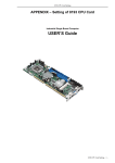
F u l l-s i z e C P U C a r d
F S B- 8 6 5 G
FSB-865G
®
Intel Pentium ® 4 &
Celeron® Processors
Full-size CPU Card
With DDR, Ethernet,
CompactFlash™ & Mini PCI
FSB-865G Rev. A Manual 2nd Ed.
Dec. 2004
F u l l-s i z e C P U C a r d
F S B- 8 6 5 G
Copyright Notice
This document is copyrighted, 2004. All rights are reserved. The original
manufacturer reserves the right to make improvements to the products
described in this manual at any time without notice.
No part of this manual may be reproduced, copied, translated, or transmitted
in any form or by any means without the prior written permission of the
original manufacturer. Information provided in this manual is intended to be
accurate and reliable. However, the original manufacturer assumes no
responsibility for its use, or for any infringements upon the rights of third
parties that may result from its use.
The material in this document is for product information only and is subject
to change without notice. While reasonable efforts have been made in the
preparation of this document to assure its accuracy, AAEON assumes no
liabilities resulting from errors or omissions in this document, or from the
use of the information contained herein.
AAEON reserves the right to make changes in the product design without
notice to its users.
i
F u l l-s i z e C P U C a r d
F S B- 8 6 5 G
Acknowledgments
All other product s’name or trademarks are properties of their respective
owners.
l
Award is a trademark of Award Software International, Inc.
l
CompactFlash™ is a trademark of the Compact Flash Association.
l
Intel® , Pentium® M, and Celeron® M are trademarks of Intel®
Corporation.
l
Microsoft Windows is a registered trademark of Microsoft Corp.
l
ITE is a trademark of Integrated Technology Express, Inc.
l
IBM, PC/AT, PS/2, and VGA are trademarks of International Business
Machines Corporation.
l
SoundBlaster is a trademark of Creative Labs, Inc.
®
ii
F u l l-s i z e C P U C a r d
F S B- 8 6 5 G
Packing List
Before you begin installing your card, please make sure that the
following materials have been shipped:
•
1
FSB-865G CPU Card
•
1
Floppy Cable
•
1
ATA-100 Cable
•
1
USB Cable
•
1
KB Cable
•
1
Serial + Parallel Cable
•
1
Serial Cable
•
1
ATX Cable
•
1
Quick Installation Guide
•
1
CD-ROM for manual (in PDF format) and drivers
If any of these items should be missing or damaged, please contact your
distributor or sales representative immediately.
iii
F u l l-s i z e C P U C a r d
F S B- 8 6 5 G
Contents
Chapter 1 General Information
1.1 Introduction ..................................................................................1-2
1.2 Feature...........................................................................................1-4
1.3 Specification ..................................................................................1-5
Chapter 2 Quick Installation Guide
2.1 Safety Precaution..........................................................................2-2
2.2 Location of Connector and Jumper ...........................................2-3
2.3 Mechanical Drawing.....................................................................2-5
2.4 List of Jumpers .............................................................................2-7
2.5 List of Connectors ........................................................................2-8
2.6 Setting Jumpers.............................................................................2-10
2.7 Clear CMOS (JP1) ........................................................................2-11
2.8 LCD Voltage Selection (JP2) ......................................................2-11
2.9 Front panel Connector (FP1)......................................................2-11
2.10 Front panel Connector (FP2)....................................................2-12
2.11 TV-Out Connector (TV1) .........................................................2-12
2.12 RS-232 Serial Port Connector (COM1) ...................................2-12
2.13 RS-232/422/485 Serial Port Connector (COM2) ..................2-13
2.14 IrDA Connector (IR1)...............................................................2-13
2.15 LPT Port Connector (LPT1) ....................................................2-14
2.16 USB Connector (USB1~3)........................................................2-14
2.17 Fan Connector (CN1) ................................................................2-15
iv
F u l l-s i z e C P U C a r d
F S B- 8 6 5 G
2.18 ATX Power Control Connector (CN2) ...................................2-15
2.19 Audio Connector (CN3)............................................................2-15
2.20 PS/2 keyboard & Mouse Connector (CN4) ...........................2-16
2.21 Internal Keyboard Connector (CN5).......................................2-16
2.22 LVDS Channel Connector (CN6) ............................................2-17
2.23 LAN LED Connector (CN7~8) ..............................................2-17
Chapter 3 Award BIOS Setup
3.1 System Test and Initialization. ....................................................3-2
3.2 Award BIOS Setup.......................................................................3-3
3.3 Standard CMOS Features ............................................................3-6
3.4 Advanced BIOS Features ............................................................3-7
3.5 Advanced Chipset Features .........................................................3-9
3.6 Integrated Peripherals ..................................................................3-10
3.7 Power management Setup...........................................................3-11
3.8 PnP/PCI configuration ...............................................................3-12
3.9 PC Health Status...........................................................................3-13
3.10 Frequency / Voltage control.....................................................3-14
3.11 Load Fail-Safe Defaults .............................................................3-15
3.12 Load Optimized Defaults..........................................................3-16
3.13 Set Supervisor / User Password ...............................................3-17
3.14 Save & Exit Setup.......................................................................3-18
3.15 Exit without saving ....................................................................3-19
Chapter 4 Driver Installation
4.1 Installations ...................................................................................4-3
v
F u l l-s i z e C P U C a r d
F S B- 8 6 5 G
Appendix A I/O Information
A.1 I/O Address Map ................................................................... A-2
A.2 1st MB Memory Address Map ............................................... A-3
A.3 IRQ Mapping Chart ............................................................... A-4
A.4 DMA Channel Assignments ................................................. A-5
Appendix B Programming The Watchdog Timer
B.1 Programming............................................................................B-2
B.2 W83627HF Watchdog Timer Initial Program......................B-6
vi
F u l l-s i z e C P U C a r d
F S B- 8 6 5 G
1
Chapter
General
Information
Chapter 1 General Information
1- 1
F u l l-s i z e C P U C a r d
F S B- 8 6 5 G
1.1 Introduction
Introducing AAEON’s new FSB-865G, powered by Intel®
Pentium® 4/Prescott processor, full size form factor single board computer
(SBC) with an onboard VGA, 10/100/1000Mb LAN optional and seven
USB 2.0 ports.
FSB-865G successfully deployed Intel® most advanced 82865GV chipset,
which supports high CPU frequency up to 3.2 GHz with front side bus
running at 400/533/800MHz. FSB-865G supports Intel® Hyper-Threading
Technology gives you the best overall Pentium ® 4/Prescott processor
performance available. FSB-865G also provides high memory capacity up to
4 GB DDR DRAM (DDR 200/266/333/400) and support Dual-channel
(128 bits wide) DDR memory interface.
In addition to its powerful computing engine, the full functional design of
the board includes features such as i82865GV on-chip integrated 2D/3D
graphics engine, built-in USB 2.0 and on board CompactFlash™ Type II
socket. FSB-865G delivers super graphic performance without additional
cost on integrated Intel® 82865GV chipset, and provides unique Intel®
Extreme Graphics architecture to maximize VGA performance capability.
Seven USB 2.0 ports provide an expandable, Plug and Play serial interface
that ensures a standard low-cost connection for peripheral devices.
Chapter 1 General Information
1 -2
F u l l-s i z e C P U C a r d
F S B- 8 6 5 G
Industrial applications will benefit from the seven USB 2.0 by three
pin-headers and one Type A connector onboard, offering 480Mbps
high-speed efficiency and value without compromising performance.
Moreover, FSB-865G is also equipped with Dual Intel® Ethernet controllers.
One of these provides superior 1 GB Mbps networking access ability for
high speed networking applications such as gateway, VPN, Mini server.
In short, this product is a versatile Pentium® 4/ Prescott compact board
with the best cost-performance for CTI, networking and mini-server
markets.
Chapter 1 General Information
1 -3
F u l l-s i z e C P U C a r d
F S B- 8 6 5 G
1.2 Feature
•
Support Intel® Pentium® 4 CPU up to 3.2GHz (Prescott
CPU)
•
Integrated AC-97 Codec Audio (Daughter Board optional)
•
Support Ultra ATA100 & SATA & CompactFlash™ Type II
Storage
•
Support 7 USB 2.0 Port
•
Support RS-232 x 1, RS-232/422/485 x 1
•
Support 1 parallel port
•
Support 1 IrDA port
•
Integrated AGP 8X 2D/3D Graphics Accelerator, VGA
Support
•
Support DDR400 Memory up to 4GB
•
Watchdog Function 1~255 sec.
•
Support Dual Channel DDR Memory Interface
Chapter 1 General Information
1 -4
F u l l-s i z e C P U C a r d
F S B- 8 6 5 G
1.3 Specification
System
l
CPU:
R
Support Intel Pentium® 4
R
and Celeron Processors up to
3.2 GHz (400/533/800MHz
FSB)
l
Chipset:
Intel® 865GV + Intel®
82801EB/ER (ICH5/ICH5R)
l
I/O Chipset:
Winbond W83627HF
l
Ethernet:
10/100Mb or 10/100/1000Mb
LAN optional, RJ-45 x 2 Intel®
82562EZ / 82547GI /
82551QM / 82541GI
controller
l
System Memory:
184 pins 2.5V DDR DIMM
Socket x 4, total up to 4GB
Support Dual Channel DDR
memory (DDR266/333/400)
l
BIOS:
Award Plug & Play ISA BIOS –
4Mb ROM
l
Watchdog Timer:
1~255 sec., can be set with
software on Super I/O
l
SSD:
Type II CompactFlash™ slot x 1
l
Expansion Interface:
Type III Mini PCI socket x 1
Chapter 1 General Information
1 -5
F u l l-s i z e C P U C a r d
l
Battery:
l
Power Supply Voltage:
F S B- 8 6 5 G
Lithium battery
+12V ATX, other supply from
Backplane
l
VGA Controller:
Integrated on Intel® 865GV,
AGP, Core frequency up to
266MHz
l
LCD Controller:
Chrontel CH7017A support
TV-Out and LVDS output
l
Audio Daughter board:
Realtek ALC655 AC97 Codec,
(Optional)
MIC-in/Line-in/Line-out/CD-I
N
l
IDE Interface:
ATA-100 x 2 channel (Suppport
two ATAPI devices)
SATA-150 x 2 (Support two
SATA devices, Raid function
optional)
l
Universal Serial Bus:
USB 2.0 Port x 7
5 x 2 pin header for internal x 3
Type-A connector onboard x 1
l
IR Interface:
Support IrDA header x 1
l
RTC:
Internal RTC
l
Operation Temp:
0℃~60℃
Display
l
Chip:
Chapter 1 General Information
Intel® 82865GV
1 -6
F u l l-s i z e C P U C a r d
F S B- 8 6 5 G
l
Memory size:
Shared memory up to 64 MB
l
Resolutions:
Up to 2048 X 1536 @ 75MHz
for CRT
I/O
l
Enhanced IDE Interface
ATA-100 x 2 channel (support
4 ATAPI devices)
l
FDD Interface:
Standard FDD port x 1
(support up to 2 floppy devices)
l
Serial Ports:
COM 1: RS-232
COM 2: RS-232/422/485
l
Parallel Port:
Support SPP/EPP/ECP mode
l
KB & Mouse connector:
Mini-DIN for PS/2 KB and
mouse connector x 1
Internal keyboard pin header x
1
l
IrDA:
IrDA Tx/Rx header x 1
l
USB
Three 5 x 2 pin headers
(support 7 USB 2.0 ports)
Chapter 1 General Information
1 -7
F u l l-s i z e CPU Card
F S B- 8 6 5 G
2
Chapter
Quick
Installation
Guide
Notice:
The Quick Installation Guide is derived
from Chapter 2 of user manual. For other
chapters
and
further
installation
instruction s, please refer to the user
manual CD -ROM that came with the
product.
Part No. 2007865010 Printed in Taiwan Nov. 2004
Chapter 2 Quick Installation Guide
2 -1
F u l l-s i z e CPU Card
F S B- 8 6 5 G
2.1 Safety Precaution
Always completely disconnect the power cord from
your board whenever you are working on it. Do not
make connections while the power is on, because a
sudden rush of power can damage sensitive
electronic components.
Always ground yourself to remove any static charge
before touching the board. Modern electronic
devices are very sensitive to static electric charges.
Use a grounding wrist strap at all times. Place all
electronic components on a static-dissipative
surface or in a static-shielded bag when they are not
in the chassis
Chapter 2 Quick Installation Guide
2 -2
F u l l-s i z e CPU Card
F S B- 8 6 5 G
2.2 Location of Connectors and Jumpers
Component Side
JP2
FAN
ATX2
CN6
TV1
ATX1
CN2
DIM1
DIM2
DIM3
DIM4
MPCI1
FP2
FP1
LPT1
USB3
USB2
USB1
CN3
IR1
W83627HF-AW
JP1
Winbond
COM1
COM2
IDE1
SATA2
SATA1
IDE2
CN8
FDD1
CN7
CN5
USB4
LAN1
VGA1
LAN2
CN4
Chapter 2 Quick Installation Guide
2 -3
F u l l-s i z e CPU Card
F S B- 8 6 5 G
Solder Side
CFD1
Chapter 2 Quick Installation Guide
2 -4
F u l l-s i z e CPU Card
F S B- 8 6 5 G
2.3 Mechanical Drawing
98.60
0.00
13.41
19.51
Component Side
3.02
0.00
1.47
12.79
10.36
28.79
28.78
94.56
65.74
94.56
13.92
76.40
90.37
98.60
100.38
197.82
208.48
228.30
232.36
236.42
237.19
238.71
W inbond
W83627HF-AW
276.30
273.76
100.38
33.26
38.66
286.82
292.29
256.24
94.28
40.82
9.70
3.51
268.30
318.68
318.34
329.44
318.62
322.85
324.43
330.40
331.50
335.48
326.94
102.49
100.51
98.50
92.25
82.73
72.57
53.42
38.25
2.49
8.84
15.70
92.08
78.64
53.43
Chapter 2 Quick Installation Guide
14.10
12.55
6.28
13.40
14.50
6.50
1.60
27.71
9.37
2 -5
F u l l-s i z e CPU Card
F S B- 8 6 5 G
Solder Side
98.50
CFD1
56.43
19.51
335.48
331.50
256.75
89.61
30.18
1.73
0.00
3.02
102.49
98.50
74.47
0.00
Chapter 2 Quick Installation Guide
2 -6
F u l l-s i z e CPU Card
F S B- 8 6 5 G
2.4 List of Jumpers
The board has a number of jumpers that allow you to configure your system
to suit your application.
The table below shows the function of each of the board's jumpers:
Jumpers
Label
Function
JP1
Clear CMOS
JP2
LCD Voltage Selection
Chapter 2 Quick Installation Guide
2 -7
F u l l-s i z e CPU Card
F S B- 8 6 5 G
2.5 List of Connectors
The board has a number of connectors that allow you to configure your
system to suit your application. The table below shows the function of each
board's connectors:
Connectors
Label
Function
FAN
Fan Connector
CN2
ATX Power Control Connector
CN3
AC97 Connector
CN4
PS/2 keyboard/Mouse Connector
CN5
Internal keyboard Connector
CN6
LVDS Channel Connector
CN7
LAN 1 Active LED Connector
CN8
LAN 2 Active LED Connector
FP1
Front Panel Connector 1
FP2
Front Panel Connector 2
ATX1
ATX Power Connector
ATX2
ATX Power_12V Connector
VGA1
VGA Display Connector
TV1
TV_Out Connector
FDD1
Floppy Connector
IDE1~2
EIDE Connector
SATA1~2
Serial ATA Connector
Chapter 2 Quick Installation Guide
2 -8
F u l l-s i z e CPU Card
F S B- 8 6 5 G
CFD1
CompactFlash Slot
COM1
RS-232 Serial Port Connector
COM2
RS-232/422/485 Serial Port Connector
IR1
IrDA Connector
LPT1
LPT Port Connector
USB1~3
USB Connector
USB4
USB Connector
LAN1
10/100 or 100/1000Base-Tx Ethernet Connector
LAN2
10/100 or 100/1000Base-Tx Ethernet Connector
MPCI1
Mini PCI Slot
DIMM1~4
DIMM Slot
Chapter 2 Quick Installation Guide
2 -9
F u l l-s i z e CPU Card
F S B- 8 6 5 G
2.6 Setting Jumpers
You configure your card to match the needs of your application by setting
jumpers. A jumper is the simplest kind of electric switch. It consists of two
metal pins and a small metal clip (often protected by a plastic cover) that
slides over the pins to connect them. To “close” a jumper you connect the
pins with the clip.
To “open” a jumper you remove the clip. Sometimes a jumper will have three
pins, labeled 1, 2 and 3. In this case you would connect either pins 1 and 2 or
2 and 3.
3
1 2
Open
Closed
Closed 2-3
A pair of needle-nose pliers may be helpful when working with jumpers.
If you have any doubts about the best hardware configuration for your
application, contact your local distributor or sales representative before you
make any change.
Generally, you simply need a standard cable to make most connections.
Chapter 2 Quick Installation Guide
2 - 10
F u l l-s i z e CPU Card
F S B- 8 6 5 G
2.7 Clear CMOS (JP1)
JP1
Function
Close
Clear
Open
Protected (Default)
2.8 LCD Voltage Selection (JP2)
JP2
Function
1-2
+5V
2-3
+3.3 V (Default)
2.9 Front Panel Connector (FP 1)
Pin
Signal
Pin
Signal
1
Power On Button (+)
2
Reset Switch (+)
3
Power On Button (-)
4
Reset Switch (-)
5
IDE LED (+)
6
Power LED (+)
7
IDE LED (-)
8
Power LED (-)
Chapter 2 Quick Installation Guide
2 - 11
F u l l-s i z e CPU Card
F S B- 8 6 5 G
2.10 Front Panel Connector (FP2)
Close Pin 5-7: Internal Buzzer Enable
Close Pin 1-7: External Speaker Enable
Pin
Signal
Pin
Signal
1
External Speaker (+)
2
Keyboard Lock (+)
3
N.C.
4
GND
5
Internal Buzzer (-)
6
I2C Bus SMB Clock
7
External Speaker (-)
8
I2C Bus SMB DATA
2.11 TV-Out Connector (TV1)
Pin
Signal
Pin
Signal
1
Y
2
CVBS
3
GND
4
GND
5
C
6
N.C.
7
GND
8
N.C.
2.12 RS -232 Serial Port Connector (COM1)
Pin
Signal
Pin
Signal
1
DCD
2
RXD
3
TXD
4
DTR
5
GND
6
DSR
7
RTS
8
CTS
9
RI
10
N.C.
Chapter 2 Quick Installation Guide
2 - 12
F u l l-s i z e CPU Card
F S B- 8 6 5 G
2.13 RS -232/422/485 Serial Port Connector (COM2)
Pin
Signal
Pin
Signal
1
DCD
2
RXD (422RXD+)
4
DTR (422RXD-)
(422TXD-/485DATA-)
3
TXD
(422TXD+/485DATA+)
5
GND
6
DSR
7
RTS
8
CTS
9
RI
10
N.C.
2.14 IrDA Connector (IR1)
Pin
Signal
1
+5V
2
N.C.
3
IRRX
4
GND
5
IRTX
6
N.C.
2.15 LPT Port Connector (LPT1)
Pin
Signal
Pin
Signal
1
#STROBE
2
#AFD
3
DATA0
4
#ERROR
5
DATA1
6
#INIT
Chapter 2 Quick Installation Guide
2 - 13
F u l l-s i z e CPU Card
F S B- 8 6 5 G
7
DATA2
8
#SLIN
9
DATA3
10
GND
11
DATA4
12
GND
13
DATA5
14
GND
15
DATA6
16
GND
17
DATA7
18
GND
19
#ACK
20
GND
21
BUSY
22
GND
23
PE
24
GND
25
SELECT
26
N.C.
2.16 USB Connector (USB1~3)
Pin
Signal
Pin
Signal
1
+5V
2
GND
3
USBD1-
4
GND
5
USBD1+
6
USBD2+
7
GND
8
USBD2-
9
GND
10
+5V
Chapter 2 Quick Installation Guide
2 - 14
F u l l-s i z e CPU Card
F S B- 8 6 5 G
2.17 Fan Connector (CN1)
Pin
Signal
1
GND
2
+12V
3
Speed Sense
2.18 ATX Power Control Connector (CN2)
AT Power Use: Close Pin 2, 3
Pin
Signal
1
PS-ON
2
+5V
3
5VSB
2.19 Audio Connector (CN3)
Pin
Signal
Pin
Signal
1
AC_RST-
2
AC_SYNC
3
AC_DAIN2
4
AC_DAOUT
5
GND
6
AC_BCLK
7
GND
8
+5V
9
LOCK
10
+3.3V
Chapter 2 Quick Installation Guide
2 - 15
F u l l-s i z e CPU Card
F S B- 8 6 5 G
2.20 PS/2 keyboard & Mouse Connector (CN4)
Pin
Signal
1
KB_DATA
2
MS_DATA
3
GND
4
+5V
5
KB_CLK
6
MS_CLK
2.21 Internal keyboard Connector (CN5)
Pin
Signal
1
KB_CLK
2
KB_DATA
3
N.C.
4
GND
5
+5V
Chapter 2 Quick Installation Guide
2 - 16
F u l l-s i z e CPU Card
F S B- 8 6 5 G
2.22 LVDS Channel Connector (CN6)
Pin
Signal
Pin
Signal
1
BKLEN
2
BKLCTL
3
PPVCC
4
GND
5
CH1_CLK#
6
CH1_CLK
7
PPVCC
8
GND
9
CH1_TX0#
10
CH1_TX0
11
CH1_TX1#
12
CH1_TX1
13
CH1_TX2#
14
CH1_TX2
15
CH1_TX3#
16
CH1_TX3
17
I2C_DATA
18
I2C_CLK
19
CH2_TX0#
20
CH2_TX0
21
CH2_TX1#
22
CH2_TX1
23
CH2_TX2#
24
CH2_TX2
25
CH2_TX3#
26
CH2_TX3
27
PPVCC
28
GND
29
CH2_CLK#
30
CH2_CLK
2.23 LAN LED Connector (CN7~8)
Pin
Signal
Pin
Signal
1
Link_LED (-)
2
Active_LED (+)
Chapter 2 Quick Installation Guide
2 - 17
F u l l-s i z e C P U C a r d
F S B- 8 6 5 G
3
Chapter
Award
BIOS Setup
Chapter 3 Award BIOS Setup
3-1
F u l l-s i z e C P U C a r d
F S B- 8 6 5 G
3.1 System Test and Initialization
These routines test and initialize board hardware. If the routines
encounter an error during the tests, you will either hear a few short
beeps or see an error message on the screen. There are two kinds of
errors: fatal and non-fatal. The system can usually continue the boot
up sequence with non-fatal errors. Non-fatal error messages usually
appear on the screen along with the following instructions:
Press <F1> to RESUME
Write down the message and press the F1 key to continue the boot
up sequence.
System configuration verification
These routines check the current system configuration against the
values stored in the CMOS memory. If they do not match, the
program outputs an error message. You will then need to run the
BIOS setup program to set the configuration information in
memory.
There are three situations in which you will need to change the
CMOS settings:
1.
You are starting your system for the first time
2.
You have changed the hardware attached to your system
3.
The CMOS memory has lost power and the configuration
information has been erased.
The FSB-865G CMOS memory has an integral lithium battery
backup for data retention. However, you will need to replace the
complete unit when it finally runs down.
Chapter3 Award BIOS Setup
3 -2
F u l l-s i z e C P U C a r d
F S B- 8 6 5 G
3.2 Award BIOS Setup
Awards BIOS ROM has a built-in Setup program that allows users to
modify the basic system configuration. This type of information is
stored in battery-backed CMOS RAM so that it retains the Setup
information when the power is turned off.
Entering setup
Power on the computer and press <Del> immediately. This will
allow you to enter Setup.
Standard CMOS Features
Use this menu for basic system configuration. (Date, time, IDE, etc.)
Advanced BIOS Features
Use this menu to set the advanced features available on your system.
Advanced Chipset Features
Use this menu to change the values in the chipset registers and
optimize your system performance.
Chapter3 Award BIOS Setup
3 -3
F u l l-s i z e C P U C a r d
F S B- 8 6 5 G
Integrated Peripherals
Use this menu to specify your settings for integrated peripherals.
(Primary slave, secondary slave, keyboard, mouse etc.)
Power Management Setup
Use this menu to specify your settings for power management.
(HDD power down, power on by ring etc.)
PnP/PCI Configurations
This entry appears if your system supports PnP/PCI.
PC Health Status
This menu shows you the status of PC.
Frequency/Voltage Control
This menu shows you the display of frequency/Voltage Control.
Load Fail-Safe Defaults
Use this menu to load the BIOS default values for the
minimal/stable performance for your system to operate.
Load Optimized Defaults
Use this menu to load the BIOS default values that are factory
settings for optimal performance system operations. While AWARD
has designated the custom BIOS to maximize performance, the
factory has the right to change these defaults to meet their needs.
Set Supervisor/User Password
Use this menu to set Supervisor/User Passwords.
Save and Exit Setup
Save CMOS value changes to CMOS and exit setup.
Chapter3 Award BIOS Setup
3 -4
F u l l-s i z e C P U C a r d
F S B- 8 6 5 G
Exit Without Saving
Abandon all CMOS value changes and exit setup.
Chapter3 Award BIOS Setup
3 -5
F u l l-s i z e C P U C a r d
F S B- 8 6 5 G
3.3 Standard CMOS Features
When you choose the Standard CMOS Features option from the
INITIAL SETUP SCREEN menu, the screen shown below is
displayed. This standard Setup Menu allows users to configure
system components such as date, time, hard disk drive, floppy drive
and display. Once a field is highlighted, on-line help information is
displayed in the right box of the Menu screen.
Chapter3 Award BIOS Setup
3 -6
F u l l-s i z e C P U C a r d
F S B- 8 6 5 G
3.4 Advanced BIOS Features
By choosing the Advanced BIOS Features option from the INITIAL
SETUP SCREEN menu, the screen below is displayed. This sample
screen contains the manufacturer’s default values for the FSB-865G
Chapter3 Award BIOS Setup
3 -7
F u l l-s i z e C P U C a r d
l
CPU Feature
l
Hard Disk Boot Priority
Chapter3 Award BIOS Setup
F S B- 8 6 5 G
3 -8
F u l l-s i z e C P U C a r d
F S B- 8 6 5 G
3.5 Advanced Chipset Features
By choosing the Advanced Chipset Features option from the
INITIAL SETUP SCREEN menu, the screen below is displayed.
This sample screen contains the manufacturer’s default values for the
FSB-865G.
Chapter3 Award BIOS Setup
3 -9
F u l l-s i z e C P U C a r d
F S B- 8 6 5 G
3.6 Integrated Peripherals
By choosing the Integrated Peripherals from the INITIAL SETUP
SCREEN menu, the screen below is displayed. This sample screen
contains the manufacturer’s default values for the FSB-865G.
Chapter3 Award BIOS Setup
3 - 10
F u l l-s i z e C P U C a r d
F S B- 8 6 5 G
3.7 Power management Setup
By choosing the Power Management Setup from the INITIAL
SETUP SCREEN menu, the screen below is displayed. This sample
screen contains the manufacturer’s default values for the FSB-865G.
Chapter3 Award BIOS Setup
3 - 11
F u l l-s i z e C P U C a r d
F S B- 8 6 5 G
3.8 PnP/PCI configuration
By choosing the PnP/PCI configurations from the Initial Setup
Screen menu, the screen below is displayed. This sample screen
contains the manufacturer’s default values for the FSB-865G.
Chapter3 Award BIOS Setup
3 - 12
F u l l-s i z e C P U C a r d
F S B- 8 6 5 G
3.9 PC Health Status
By choosing the PC Health Status from the Initial Setup Screen
menu, the screen below is displayed. This sample screen contains the
manufacturer’s default values for the FSB-865G.
Chapter3 Award BIOS Setup
3 - 13
F u l l-s i z e C P U C a r d
F S B- 8 6 5 G
3.10 Frequency / Voltage control
By choosing the Frequency/Voltage Control from the Initial Setup
Screen menu, the screen below is displayed. This sample screen
contains the manufacturer’s default values for the FSB-865G.
Chapter3 Award BIOS Setup
3 - 14
F u l l-s i z e C P U C a r d
F S B- 8 6 5 G
3.11 Load Fail-Safe Defaults
When you press <Enter> on this item you get a confirmation dialog
box with a message similar to:
Load Fail-Safe Default (Y/N)?
Pressing "Y" loads the BIOS default values for the most stable,
minimal performance system operations.
Chapter3 Award BIOS Setup
3 - 15
F u l l-s i z e C P U C a r d
F S B- 8 6 5 G
3.12 Load Optimized Defaults
When you press <Enter> on this item you get a confirmation dialog
box with a message similar to:
Load Optimized Defaults (Y/N)?
Pressing "Y" loads the default values that are manufacturer’s settings
for optimal performance system operations.
Chapter3 Award BIOS Setup
3 - 16
F u l l-s i z e C P U C a r d
F S B- 8 6 5 G
3.13 Set Supervisor / User Password
You can set either SUPERVISOR or USER PASSWORD, or both of
them. The difference between the two is that the supervisor password
allows unrestricted access to enter and change the options of the setup
menus, while the user password only allows entry to the program, but
not modify options.
To abort the process at any time, press Esc.
In the Security Option item in the BIOS Features Setup screen, select
System or Setup:
System
Enter a password each time the system boots and whenever you enter Setup.
Setup
Enter a password whenever you enter Setup.
NOTE: To clear the password, simply press Enter when asked to enter a
password. Then the password function is disabled.
Chapter3 Award BIOS Setup
3 - 17
F u l l-s i z e C P U C a r d
F S B- 8 6 5 G
3.14 Save & Exit Setup
If you select this option and press <Enter>, the values entered in the
setup utilities will be recorded in the chipset’s CMOS memory. The
microprocessor will check this every time you turnon your system and
compare this to what it finds as it checks the system. This record is
required for the system to operate.
Chapter3 Award BIOS Setup
3 - 18
F u l l-s i z e C P U C a r d
F S B- 8 6 5 G
3.15 Exit without saving
Selecting this option and pressing <Enter> allows you to exit the
Setup program without recording any new value or changing old one.
Chapter3 Award BIOS Setup
3 - 19
F u l l-s i z e C P U C a r d
F S B- 8 6 5 G
4
Chapter
Driver
Installation
Chapter 4 Driver Installation
4-1
F u l l-s i z e C P U C a r d
F S B- 8 6 5 G
The FSB-865G comes with a CD-ROM that contains all drivers and
utilities that meet your needs.
Follow the sequence below to install the drivers:
Step 1 – Install Intel® INF Update
Step 2 – Install Graphic Driver
Step 3 – Install Ethernet Driver
Step 4 – Install AC97 Audio Driver
Step 5 – Install Application Accelerator Driver
Step 6 – Utility (Optional)
Please read instructions below for further detailed installations.
Chapter4 Drivers Installation
4 -2
F u l l-s i z e C P U C a r d
F S B- 8 6 5 G
4.1 Installation:
Insert the FSB-865G CD-ROM into the CD-ROM Drive. And install
the drivers from Step 1 to Step 6 in order.
Step 1 – Install Intel® INF Update
1.
Click on the Intel ® INF Update folder and then double click
on the setup.exe.
2.
Follow the instructions that the window will show you.
3.
The system will help you install the driver automatically.
4.
Please re-start your computer.
Step 2 – Install Graphic Driver
1.
Click on the Graphic Driver folder
2.
Choose the OS folder that meets your system
3.
Double click on the setup.exe. where is located on each OS
foler.
4.
Follow the instructions that the window will show you.
5.
The system will help you install the driver automatically.
6.
Please re-start your computer.
Step 3 – Install Ethernet Driver
1.
Click on the Ethernet Driver folder and then double click on
the setup.exe.
2.
Follow the instructions that the window will show you.
3.
The system will help you install the driver automatically.
4.
Please re-start your computer.
Chapter4 Drivers Installation
4 -3
F u l l-s i z e C P U C a r d
F S B- 8 6 5 G
Step 4 – Install AC97 Audio Driver
1.
Click on the AC97 Audio Driver folder and then enter ALC655
folder.
2.
Choose the OS folder that meets your system and execute on the
setup. exe.
3.
Follow the instructions that the window will show you.
4.
The system will help you install the driver automatically.
5.
Please re-start your computer.
Step 5 – Install Application Accelerator driver (For RF version only)
1.
Click on the Application Accelerator folder and then enter
IAA folder.
2.
Double click on the setup. exe.
3.
Follow the instructions that the window will show you.
4.
The system will help you install the driver automatically.
5.
Please re-start your computer.
Step 6 – Utility driver (Optional)
1.
Execute on the setup. exe after entering Utility driver folder.
2.
Follow the instructions that the window will show you.
3.
The system will help you install the driver automatically.
4.
Please re-start your computer.
Note:
Under the Window® OS environment, if the CRT connector is
connected to display monitor by the data switch device, the user need
to set the color and resolution from Intel® Graphic utility (VGA
driver) instead of setting from the control panel in case of the wrong
display appearance.
Chapter4 Drivers Installation
4 -4
F u l l-s i z e C P U C a r d
F S B- 8 6 5 G
A
Appendix
I/O Information
Appendix A I/O Information
A-1
F u l l-s i z e C P U C a r d
F S B- 8 6 5 G
A.1 I/O Address Map
Appendix A I/O Informaion
A-2
F u l l-s i z e C P U C a r d
F S B- 8 6 5 G
st
A.2 1 MB Memory Address Map
Appendix A I/O Informaion
A-3
F u l l-s i z e C P U C a r d
F S B- 8 6 5 G
A.3 IRQ Mapping Chart
Appendix A I/O Informaion
A-4
F u l l-s i z e C P U C a r d
F S B- 8 6 5 G
A.4 DMA Channel Assignments
Appendix A I/O Informaion
A-5
F u l l-s i z e C P U C a r d
F S B- 8 6 5 G
B
Appendix
Programming the
Watchdog Timer
Appendix B Programming the Watchdog Timer
B-1
F u l l-s i z e C P U C a r d
F S B- 8 6 5 G
B.1 Programming
FSB-865G utilizes W83627HF chipset as its watchdog timer
controller.
Below are the procedures to complete its configuration and the
AAEON intial watchdog timer program is also attached based on
which you can develop customized program to fit your application.
Configuring Sequence Description
Unlock W83627H
Select register of
watchdog timer
Enable the
function of the
watchdog timer
Use the function of
the watchdog
timer
Lock W83627HF
Appendix B Programming the Wa tchdog Timer
B-2
F u l l-s i z e C P U C a r d
F S B- 8 6 5 G
There are three steps to complete the configuration setup:
(1) Enter the W83627HF config Mode
(2) Modify the data of configuration registers
(3) Exit the W83627HF config Mode. Undesired result may occur if
the config Mode is not exited normally.
(1) Enter the W83627HF config Mode
To enter the W83627HF config Mode, two special I/O write
operations are to be performed during Wait for Key state. To ensure
the initial state of the key-check logic, it is necessary to perform two
write operations to the Special Address port (2EH). The different
enter keys are provided to select configuration ports (2Eh/2Fh) of
the next step.
87h,87h:
Address Port
Data Port
2Eh
2Fh
(2) Modify the Data of the Registers
All configuration registers can be accessed after entering the config
Mode. Before accessing a selected register, the content of
Index 07h must be changed to the LDN to which the register
belongs, except some Global registers.
(3) Exit the W83627HF config Mode
The exit key is provided to select configuration ports (2Eh/2Fh) of
the next step.
Address Port
0aah:
2Eh
Appendix B Programming the Wa tchdog Timer
Data Port
2Fh
B-3
F u l l-s i z e C P U C a r d
F S B- 8 6 5 G
WatchDog Timer Register I (Index=F5h, Default=00h)
CRF5 (PLED mode register. Default 0 x 00)
Bit 7-6
: select PLED mode
= 00 Power LED pin is tri-stated.
= 01 Power LED pin is drived low.
= 10 Power LED pin is a 1Hz toggle pulse with
50 duty cycle.
= 11 Power LED pin is a 1/4Hz toggle pulse
with 50 duty cycle.
Bit 5-4
: Reserved
Bit 3
: select WDTO count mode.
Bit 2
=0
second
=1
minute
: Enable the rising edge of keyboard Reset (P20) to
force Time-out event.
= 0 Disable
= 1 Enable
Bit 1-0
: Reserved
WatchDog Timer Register II (Index=F6h, Default=00h)
Bit 7-0
= 0 x 00 Time-out Disable
= 0 x 01 Time-out occurs after 1
second/minute
= 0 x 02 Time-out occurs after 2
second/minutes
= 0 x 03 Time-out occurs after 3
Appendix B Programming the Wa tchdog Timer
B-4
F u l l-s i z e C P U C a r d
F S B- 8 6 5 G
second/minutes
… … … … … … … … … … … … ..
= 0 x FF Time-out occurs after 255
second/minutes
WatchDog Timer Register III (Index=F7h, Default=00h)
Bit 7
Bit 6
: Mouse interrupt reset Enable or Disable
=1
Watchdog Timer is reset upon a Mouse
interrupt
=0
Watchdog Timer is not affected by
Mouse interrupt
: Keyboard interrupt reset Enable or Disable
=1
Watchdog Timer is reset upon a
Keyboard interrupt
=0
Watchdog Timer is not affected by
Keyboard interrupt
Bit 5
: Force Watchdog Timer Time-out. Write
Only
=1
Force Watchdog Timer time-out
event: this bit is self-clearing
Bit 4
Bit 3-0
: Watchdog Timer Status. R/W
=1
Watchdog Timer time-out occurred
=0
Watchdog Timer counting
: These bits select IRQ resource for
Watchdog. Setting of 2 selects SMI.
Appendix B Programming the Wa tchdog Timer
B-5
F u l l-s i z e C P U C a r d
F S B- 8 6 5 G
B.2 W83627HF Watchdog Timer Initial Program
Example: Setting 10 sec. as Watchdog timeout interval
;///////////////////////////////////////////////////////////////////////////////////////////////
Mov dx,2eh
;Enter W83627HF config mode
Mov al,87h
(out 87h to 2eh twice)
Out dx,al
Out dx,al
;///////////////////////////////////////////////////////////////////////////////////////////////
Mov al,07h
Out dx,al
Inc dx
Mov al,08h
;Select Logical Device 8 (GPIO Port 2)
Out dx,al
;///////////////////////////////////////////////////////////////////////////////////////////////
Dec dx
Mov al,30h
;CR30 (GP20~GP27)
Out dx,al
Inc dx
Mov al,01h
;Activate GPIO2
Out dx,al
;///////////////////////////////////////////////////////////////////////////////////////////////
Appendix B Programming the Wa tchdog Timer
B-6
F u l l-s i z e C P U C a r d
F S B- 8 6 5 G
Dec dx
Mov al,0f5h
;CRF5 (PLED mo de register)
Out dx,al
Inc dx
In al,dx
And al,not 08h
;Set second as counting unit
Out dx,al
;///////////////////////////////////////////////////////////////////////////////////////////////
Dec dx
Mov al,0f6h
; CRF6
Out dx,al
Inc dx
Mov al,10
;Set timeout interval as 10 sec.
Out dx,al
;///////////////////////////////////////////////////////////////////////////////////////////////
Dec dx
;Exit W83627HF config mode
Mov al,0aah
(out 0aah to 2eh once)
Out dx,al
;///////////////////////////////////////////////////////////////////////////////////////////////
Appendix B Programming the Wa tchdog Timer
B-7