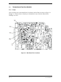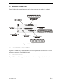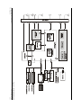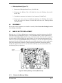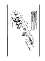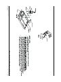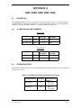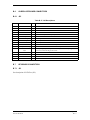
1
400 SERIES MAINTENANCE MANUAL (GNS¥430, GNC¥420, GPS 400) GNS 430 Shown GARMIN International, Inc. 1200 E. 151st Street Olathe, KS 66062 USA 190-00140-05, Revision C October 2002 © Copyright 1999-2002 GARMIN Ltd. or its subsidiaries All Rights Reserved GARMIN International, Inc. 1200 East 151st Street, Olathe, Kansas 66062, U.S.A. GARMIN (Europe) Ltd. Unit 5, The Quadrangle, Abbey Park Industrial Estate, Romsey, SO51 9AQ, U.K. GARMIN Corporation No. 68, Jangshu 2nd Road, Shijr, Taipei County, Taiwan Except as expressly provided herein, no part of this manual may be reproduced, copied, transmitted, disseminated, downloaded or stored in any storage medium, for any purpose without the express prior written consent of GARMIN. GARMIN hereby grants permission to download a single copy of this manual and of any revision to this manual onto a hard drive or other electronic storage medium to be viewed and to print one copy of this manual or of any revision hereto, provided that such electronic or printed copy of this manual or revision must contain the complete text of this copyright notice and provided further that any unauthorized commercial distribution of this manual or any revision hereto is strictly prohibited. Information in this document is subject to change without notice. GARMIN reserves the right to change or improve its products and to make changes in the content without obligation to notify any person or organization of such changes or improvements. GARMIN International, Inc. 1200 E. 151st Street Olathe, KS 66062 USA Telephone: 913-397-8200 Aviation Panel-Mount Technical Support Line (Toll Free): 1-888-606-5482 www.garmin.com RECORD OF REVISIONS REVISION REVISION DATE Description ECO # A 07/06/99 Initial Release ----- B 01/26/01 Redraw 15007 C 10/22/02 Redraw 19319 Insertion Date By GNC and GNS are trademarks of GARMIN Ltd. or its subsidiaries and may not be used without the express permission of GARMIN. Page A Rev. C 400 SERIES MAINTENANCE MANUAL P/N 190-00140-05 LIST OF EFFECTIVE PAGES Page Revision Page Revision Page Revision Page Revision A i ii iii iv v vi vii viii ix x xi xii 1-1 1-2 1-3 1-4 1-5 1-6 2-1 2-2 F2-3 F2-4 F2-5 F2-6 F2-7 F2-8 F2-9 F2-10 3-1 3-2 3-3 3-4 3-5 3-6 3-7 3-8 3-9 3-10 3-11 3-12 3-13 3-14 3-15 3-16 F3-17 F3-18 4-1 4-2 4-3 4-4 4-5 4-6 4-7 C C C C C C C C C C C C C C C C C C C C BLANK C BLANK C BLANK C BLANK C BLANK C C C C C C C C C C C C C C C BLANK C BLANK C C C C C C C 4-8 5-1 5-2 5-3 5-4 5-5 5-6 5-7 5-8 5-9 5-10 5-11 5-12 5-13 5-14 5-15 5-16 5-17 5-18 5-19 5-20 5-21 5-22 5-23 5-24 5-25 5-26 5-27 5-28 5-29 5-30 5-31 5-32 5-33 5-34 5-35 5-36 5-37 5-38 5-39 5-40 5-41 5-42 5-43 5-44 5-45 5-46 5-47 5-48 5-49 5-50 5-51 5-52 5-53 C C C C C C C C C C C C C C C C C C C C C C C C C C C C C C C C C C C C C C C C C C C C C C C C C C C C C C 5-54 6-1 6-2 6-3 6-4 6-5 6-6 6-7 6-8 6-9 6-10 6-11 6-12 6-13 6-14 6-15 6-16 6-17 6-18 6-19 6-20 6-21 6-22 6-23 6-24 6-25 6-26 6-27 6-28 6-29 6-30 7-1 7-2 F7-3 F7-4 F7-5 F7-6 F7-7 F7-8 F7-9 F7-10 F7-11 F7-12 F7-13 F7-14 F7-15 F7-16 F7-17 F7-18 F7-19 F7-20 F7-21 F7-22 F7-23 BLANK C C C C C C C C C C C C C C C C C C C C C C C C C C C C C C C C C BLANK C BLANK C BLANK C BLANK C BLANK C BLANK C BLANK C BLANK C BLANK C BLANK C F7-24 A-1 A-2 B-1 B-2 B-3 B-4 B-5 B-6 B-7 B-8 B-9 B-10 B-11 B-12 B-13 B-14 B-15 B-16 B-17 B-18 BLANK C C C C C C C C C C C C C C C C C C C C (F) INDICATES FOLDOUT PAGES-PRINT ONE SIDE ONLY 400 SERIES MAINTENANCE MANUAL P/N 190-00140-05 Page i Rev. C The following are General Safety Precautions that are not related to any specific procedure and therefore do not appear elsewhere in this maintenance manual. These are recommended precautions that personnel should understand and apply during the many phases of maintenance and repair. KEEP AWAY FROM LIVE CIRCUITS. Maintenance personnel shall observe all safety regulations at all times. Do not replace components inside the equipment when potentially lethal voltages are present. Turn off system power before making or breaking electrical connections. Regard any exposed connector, terminal board, or circuit board as a possible shock hazard. Components which retain a charge shall be discharged only when such grounding does not result in equipment damage. If a test connection to energized equipment is required, make the test equipment ground connection before probing the voltage or signal to be tested. DO NOT SERVICE ALONE. Personnel shall not under any circumstances reach into or enter any enclosure for the purpose of servicing or adjusting the equipment without immediate presence or assistance of another person capable of rendering aid. INFORMATION SUBJECT TO EXPORT CONTROL LAWS This document may contain information which is subject to the Export Administration Regulations (“EAR”) issued by the United States Department of Commerce (15 CFR, Chapter VII, Subchapter C) and which may not be exported, released, or disclosed to foreign nationals inside or outside of the United States without first obtaining an export license. A violation of the EAR may be subject to a penalty of up to 10 years imprisonment and a fine of up to US $1,000,000 under Section 2410 of the Export Administration Act of 1979. Include this notice with any reproduced portion of this document. 400 SERIES HARDWARE MOD LEVEL HISTORY The following table identifies hardware modification (Mod) Levels for the 400 Series. Mod Levels are listed with the associated service bulletin number, service bulletin date, and the purpose of the modification. The table is current at the time of publication of this manual (see date on front cover) and is subject to change without notice. Authorized GARMIN Sales and Service Centers are encouraged to access the most up-to-date bulletin and advisory information on the GARMIN Dealer Resource web site at www.garmin.com using their GARMIN-provided user name and password. Mod Level Service Bulletin Number Service Bulletin Date Purpose of Modification 1 SB0019 Nov 7, 2000 14/28V only, Comm Transmitter Fuse 2 SB0101 Feb 16, 2001 14/28V only, Remote COM Transfer 3 SB0203 Feb 1, 2002 430/420; 14/28V only (-10 and –30), Receiver Audio Compressor (recommended only if problem exists) 4 SB0207 Apr 2, 2002 430/420; Remove excessive solder from Comm Board vias Page ii P/N 190-00140-05 400 SERIES MAINTENANCE MANUAL Rev. C TABLE OF CONTENTS SECTION 1 DESCRIPTION AND OPERATION Paragraph Page 1.1 INTRODUCTION .................................................................................................... 1-1 1.1.1 Versions Covered by this Manual.................................................................... 1-1 1.2 FUNCTIONAL SUMMARY...................................................................................... 1-3 1.2.1 GPS 400.......................................................................................................... 1-3 1.2.2 GNC 420 ......................................................................................................... 1-3 1.2.3 GNS 430.......................................................................................................... 1-3 1.3 REPAIR PLAN ........................................................................................................ 1-4 1.4 SPECIFICATIONS.................................................................................................. 1-4 1.5 GENERAL DESCRIPTION ..................................................................................... 1-4 1.5.1 Main Board ...................................................................................................... 1-4 1.5.2 Com Board ..................................................................................................... 1-5 1.5.3 Nav Board ...................................................................................................... 1-5 1.5.4 GPS Module ................................................................................................... 1-5 1.5.5 Glideslope Board ............................................................................................ 1-6 1.5.6 Inverter Board.................................................................................................. 1-6 1.5.7 CDU Assembly ................................................................................................ 1-6 1.5.8 Map Board....................................................................................................... 1-6 SECTION 2 SPECIAL TOOLS AND TEST EQUIPMENT Paragraph Page 2.1 INTRODUCTION .................................................................................................... 2-1 2.2 SPECIAL TOOLS AND TEST EQUIPMENT .......................................................... 2-1 2.3 TEST PANELS AND CABLES................................................................................ 2-1 400 SERIES MAINTENANCE MANUAL P/N 190-00140-05 Page iii Rev. C SECTION 3 TROUBLESHOOTING Paragraph Page 3.1 TROUBLESHOOTING EQUIPMENT ..................................................................... 3-1 3.2 TROUBLESHOOTING ORDER.............................................................................. 3-1 3.3 TROUBLESHOOTING PROCEDURES ................................................................. 3-2 3.3.1 Fuses............................................................................................................... 3-2 3.3.2 Power Supply Checks ..................................................................................... 3-4 3.3.2.1 Current Measurements.................................................................................... 3-4 3.3.2.2 Com Board ..................................................................................................... 3-5 3.3.2.3 Glideslope Board............................................................................................. 3-6 3.3.2.4 Nav Board ....................................................................................................... 3-6 3.3.3 Processor Clock Check ................................................................................... 3-6 3.3.3.1 Internal Clock CheckMain Processor........................................................... 3-6 3.3.3.2 Internal Clock CheckGPS Processor........................................................... 3-6 3.4 STATIC MESSAGES.............................................................................................. 3-7 3.5 TESTING FAILURES............................................................................................ 3-10 3.6 EXTERNAL CONNECTORS ................................................................................ 3-15 3.7 CONNECTOR I/O DESCRIPTIONS ..................................................................... 3-15 3.8 BLOCK DIAGRAM................................................................................................ 3-15 SECTION 4 DISASSEMBLY AND ASSEMBLY Paragraph Page 4.1 INTRODUCTION................................................................................................... 4-1 4.2 REQUIRED TOOLS .............................................................................................. 4-1 4.3 NAV DATA CARD REMOVAL AND INSERTION.................................................. 4-2 4.4 UNIT DESIGN ...................................................................................................... 4-3 4.5 DISASSEMBLY PROCEDURE ............................................................................. 4-3 4.5.1 Remove the Top Cover ................................................................................... 4-3 4.5.2 Remove the CDU Assembly ........................................................................... 4-3 4.5.2.1 Disassemble the CDU Assembly ................................................................... 4-4 4.5.3 Separate the Main and Nav Chassis............................................................... 4-4 4.5.4 Remove Faulty Boards from the Main Chassis Top Cavity ............................ 4-5 4.5.5 Remove Faulty Boards from the Main Chassis Underside Cavity................... 4-5 4.5.6 Remove Faulty Boards from the Nav Chassis ............................................... 4-6 4.6 REASSEMBLY ...................................................................................................... 4-7 4.7 MEMORY BATTERY REPLACEMENT................................................................. 4-7 4.7.1 Remove the Memory Battery........................................................................... 4-8 Page iv P/N 190-00140-05 400 SERIES MAINTENANCE MANUAL Rev. C SECTION 5 ALIGNMENT, CALIBRATION, AND TESTING Paragraph Page 5.1 INTRODUCTION ................................................................................................. 5-1 5.2 RECOMMENDED TEST EQUIPMENT ............................................................... 5-1 5.3 TEST SETUP....................................................................................................... 5-3 5.4 STANDARD SIGNALS AND TEST LOADS......................................................... 5-3 5.4.1 VHF Com Transceiver..................................................................................... 5-3 5.4.1.1 Standard Loads ............................................................................................... 5-3 5.4.1.2 Standard Signals ............................................................................................. 5-4 5.4.2 Glideslope ....................................................................................................... 5-4 5.4.2.1 Standard Loads ............................................................................................... 5-4 5.4.2.2 Standard Signals ............................................................................................. 5-4 5.4.3 NAV Receiver.................................................................................................. 5-5 5.4.3.1 Standard Loads ............................................................................................... 5-5 5.4.4 VOR Standard Signals .................................................................................... 5-6 5.4.4.1 Standard Test Signals ..................................................................................... 5-6 5.4.5 Localizer Standard Signals.............................................................................. 5-7 5.4.5.1 Standard Test Signals ..................................................................................... 5-7 5.5 ALIGNMENT ........................................................................................................ 5-9 5.6 CALIBRATION ..................................................................................................... 5-9 5.6.1 Com Setup Page Fields ................................................................................ 5-10 5.6.1.1 Com Frequency............................................................................................. 5-10 5.6.1.2 Frequency Spacing ....................................................................................... 5-10 5.6.1.3 SQ 250 .......................................................................................................... 5-10 5.6.1.4 SQ 833 .......................................................................................................... 5-10 5.6.1.5 Sidetone ........................................................................................................ 5-11 5.6.1.6 MIC Gain ....................................................................................................... 5-11 5.7 TEST PROCEDURES ....................................................................................... 5-12 5.7.1 Test Mode ..................................................................................................... 5-12 5.7.2 Com Testing .................................................................................................. 5-14 5.7.2.1 Power Input Check ........................................................................................ 5-14 5.7.2.2 RF Power Out................................................................................................ 5-15 5.7.2.3 Frequency Stability and Tolerance................................................................ 5-16 5.7.2.4 Modulation Capability Test ............................................................................ 5-16 5.7.2.5 Carrier Noise Level........................................................................................ 5-17 5.7.2.6 Demodulated Audio Distortion....................................................................... 5-17 5.7.2.7 Demodulated Audio Response...................................................................... 5-17 400 SERIES MAINTENANCE MANUAL P/N 190-00140-05 Page v Rev. C SECTION 5 ALIGNMENT, CALIBRATION, AND TESTING (continued) 5.7.2.8 5.7.2.9 5.7.2.10 5.7.2.11 5.7.2.12 5.7.2.13 5.7.2.14 5.7.2.15 5.7.2.16 5.7.2.17 5.7.2.18 5.7.2.19 5.7.2.20 5.7.2.21 5.7.3 5.7.3.1 5.7.3.2 5.7.3.3 5.7.3.4 5.7.3.5 5.7.3.6 5.7.3.7 5.7.3.8 5.7.3.9 5.7.3.10 5.7.3.11 5.7.3.12 5.7.3.13 5.7.3.14 5.7.3.15 5.7.3.16 5.7.3.17 5.7.3.18 5.7.3.19 Sidetone ........................................................................................................ 5-18 MIC Intercom Test......................................................................................... 5-18 Receiver Sensitivity ....................................................................................... 5-18 TX Interlock ................................................................................................... 5-19 AGC Test....................................................................................................... 5-19 Selectivity (25 kHz Mode) ............................................................................. 5-19 Selectivity (8.33 kHz Mode) .......................................................................... 5-20 Volume Control (Audio Output) ..................................................................... 5-21 Audio Distortion Test ..................................................................................... 5-21 Audio Frequency Response .......................................................................... 5-22 Receiver Audio Compressor Test ................................................................. 5-22 Squelch Test ................................................................................................. 5-23 Frequency Modulation................................................................................... 5-24 Com Remote Transfer Input.......................................................................... 5-24 Navigation Receiver Final Tests ................................................................... 5-25 Voice/Ident Audio Output Level..................................................................... 5-25 Voice/Ident Audio Frequency Response ....................................................... 5-25 Voice/Ident Audio Distortion .......................................................................... 5-26 VOR AGC...................................................................................................... 5-26 VOR Audio Sensitivity ................................................................................... 5-26 Receiver Quieting.......................................................................................... 5-27 Ident/Voice Tone Ratio.................................................................................. 5-27 Harmonic Distortion....................................................................................... 5-27 VOR Flag Sensitivity ..................................................................................... 5-28 LOC Flag Sensitivity...................................................................................... 5-28 VOR/LOC Composite Test ............................................................................ 5-28 VOR Course Deviation Sensitivity................................................................. 5-29 Localizer Course Deviation Sensitivity .......................................................... 5-29 TO-FROM Indicator....................................................................................... 5-29 Centering Accuracy ....................................................................................... 5-29 Course Deviation Accuracy Test ................................................................... 5-30 VOR OBS Bearing Accuracy ......................................................................... 5-30 Selectivity ...................................................................................................... 5-30 Spurious Response—VOR/LOC ................................................................... 5-31 Page vi P/N 190-00140-05 400 SERIES MAINTENANCE MANUAL Rev. C SECTION 5 ALIGNMENT, CALIBRATION, AND TESTING (continued) 5.7.4 5.7.4.1 5.7.4.2 5.7.4.3 5.7.4.4 5.7.4.5 5.7.4.6 5.7.4.7 5.7.4.8 5.7.4.9 5.7.4.10 5.7.5 5.7.5.1 5.7.5.2 5.7.5.3 5.7.5.4 5.7.5.5 5.7.5.6 5.7.5.7 5.7.5.8 5.7.5.9 5.7.5.10 5.7.5.11 5.7.5.12 5.7.6 5.7.6.1 5.7.6.2 5.7.6.3 5.7.6.4 5.7.6.5 5.7.6.6 5.7.6.7 5.7.6.8 5.7.6.9 5.7.6.10 5.7.6.11 5.7.6.12 5.7.6.13 Navigation Assembly I/O Tests .................................................................... 5-32 Localizer Course Deviation Test ................................................................... 5-32 To/From Deflection Output Characteristic Test ............................................. 5-32 To/From Deflection Accuracy Test ................................................................ 5-32 Course Deviation Flag Output Characteristic Test ........................................ 5-33 Course Deviation Flag Test........................................................................... 5-33 VOR/LOC Super Flag Output Test ................................................................ 5-33 NAV Input Lines ............................................................................................ 5-34 NAV OBI Outputs .......................................................................................... 5-34 Nav Serial DME Outputs ............................................................................... 5-35 NAV Parallel DME Outputs ........................................................................... 5-35 Glideslope Final Tests................................................................................... 5-37 Glideslope Course Deviation Output Characteristic Test .............................. 5-37 Course Deviation Deflection Accuracy Test .................................................. 5-37 Course Deviation Flag Test........................................................................... 5-37 Glideslope Superflag Output Test ................................................................. 5-38 Receiver Sensitivity ....................................................................................... 5-38 Centering Accuracy ....................................................................................... 5-39 AGC............................................................................................................... 5-39 Selectivity (Bandwidth) .................................................................................. 5-39 Nose Bandwidth ............................................................................................ 5-40 Skirt Bandwidth ............................................................................................. 5-40 Spurious Response ....................................................................................... 5-40 Status Tests .................................................................................................. 5-41 Main Board Final Tests ................................................................................. 5-42 Push Button Response.................................................................................. 5-42 Rotary Knobs................................................................................................. 5-42 Map ID and Data Card Test .......................................................................... 5-42 Photocell........................................................................................................ 5-43 Lighting Bus Input ......................................................................................... 5-43 Memory Battery Voltage................................................................................ 5-44 Display Pattern Test ...................................................................................... 5-45 Fan Test ........................................................................................................ 5-45 Unit Configuration Test.................................................................................. 5-45 GPS Antenna Bias ........................................................................................ 5-45 GPS Noise..................................................................................................... 5-45 Satellite Tracking Test................................................................................... 5-46 MAIN Lateral LEFT, RIGHT Outputs ............................................................. 5-47 400 SERIES MAINTENANCE MANUAL P/N 190-00140-05 Page vii Rev. C SECTION 5 ALIGNMENT, CALIBRATION, AND TESTING (continued) 5.7.6.14 5.7.6.15 5.7.6.16 5.7.6.17 5.7.6.18 5.7.6.19 5.7.6.20 5.7.6.21 5.7.6.22 5.7.6.23 5.7.6.24 5.7.6.25 MAIN Vertical UP, DOWN Outputs................................................................ 5-47 MAIN To/From Output ................................................................................... 5-47 MAIN Lateral Flag Output.............................................................................. 5-48 MAIN Vertical Flag Output............................................................................. 5-48 MAIN Lateral Super Flag Output ................................................................... 5-48 MAIN Vertical Super Flag Output .................................................................. 5-48 Annunciate Outputs....................................................................................... 5-49 OBI Serial Interface ....................................................................................... 5-50 Discrete Switch and Altitude Inputs............................................................... 5-51 ARINC 429 Transmitters and Receivers ....................................................... 5-52 RS232 Ports .................................................................................................. 5-53 OBS............................................................................................................... 5-54 SECTION 6 PARTS AND ASSEMBLIES Paragraph Page 6.1 INTRODUCTION .................................................................................................... 6-1 6.2 TABLES .................................................................................................................. 6-1 SECTION 7 ASSEMBLY DRAWINGS 7.1 INTRODUCTION .................................................................................................... 7-1 7.2 DRAWING LIST...................................................................................................... 7-1 Page viii P/N 190-00140-05 400 SERIES MAINTENANCE MANUAL Rev. C APPENDIX A GNC 420A AND GNS 430A A.1 A.2 A.3 A.4 A.5 A.6 A.7 DESCRIPTION ....................................................................................................A-1 ‘A’ VERSION PART NUMBERS ..........................................................................A-1 TROUBLESHOOTING.........................................................................................A-1 DISASSEMBLY AND ASSEMBLY.......................................................................A-2 ALIGNMENT, CALIBRATION, AND TESTING....................................................A-2 REPLACEABLE PARTS AND ASSEMBLIES......................................................A-2 ASSEMBLY DRAWING .......................................................................................A-2 APPENDIX B CONNECTOR I/O DESCRIPTIONS B.1 B.2 B.3 B.4 B.5 B.6 B.7 B.8 B.9 B.10 B.11 B.12 B.13 I/O DESCRIPTION...............................................................................................B-1 INTERNAL AND EXTERNAL CONNECTORS ....................................................B-1 MAIN BOARD CONNECTORS............................................................................B-2 COM BOARD CONNECTORS ..........................................................................B-11 NAV BOARD CONNECTORS ...........................................................................B-12 GLIDESLOPE BOARD CONNECTORS............................................................B-15 KEYBOARD CONNECTORS ............................................................................B-15 INVERTER BOARD CONNECTORS ................................................................B-16 GPS MODULE CONNECTORS ........................................................................B-17 INTERFACE BOARD CONNECTORS ..............................................................B-17 DISPLAY MODULE CONNECTORS.................................................................B-18 DATA BASE CARD CONNECTORS .................................................................B-18 MAP BOARD CONNECTORS...........................................................................B-18 400 SERIES MAINTENANCE MANUAL P/N 190-00140-05 Page ix Rev. C LIST OF FIGURES Figure 2-1 2-2 2-3 2-4 2-5 3-1 3-2 3-3 3-4 3-5 3-6 3-7 4-1 4-2 5-1 5-2 5-3 5-4 5-5 5-6 5-7 5-8 5-9 5-10 5-11 5-12 5-13 7-1 7-2 7-3 7-4 7-4 7-5 7-6 7-7 7-8 7-9 7-10 Page Com Chassis Nut................................................................................................. 2-1 Signal And Load Drawing-J1 (Sheet 1 of 2) ........................................................ 2-3 Signal And Load Drawing-J1 (Sheet 2 of 2) ........................................................ 2-5 Signal And Load Drawing-J2 ............................................................................... 2-7 Signal And Load Drawing-J6 ............................................................................... 2-9 Main Board Fuse Locations ................................................................................. 3-2 Com Board Fuse Location/F600.......................................................................... 3-3 Com Board Fuse Location/F600 (Replaced by R611)......................................... 3-3 Nav Board Fuse Locations .................................................................................. 3-4 Processor Location (Main Board) ........................................................................ 3-7 External Connectors .......................................................................................... 3-15 400 Series Block Diagram ................................................................................. 3-17 Nav Data Card Installation And Removal ............................................................ 4-2 Memory Battery Location (Main Board) ............................................................... 4-7 40dB Attenuator Circuit........................................................................................ 5-3 Com Setup Page ................................................................................................. 5-9 R558 (Com Board)............................................................................................. 5-11 Test Pages......................................................................................................... 5-13 Modulation Measurement .................................................................................. 5-16 VOR/LOC/GS CDI Test Page ............................................................................ 5-32 Main Lighting and Main Analog Test Pages ...................................................... 5-44 GPS Test Page.................................................................................................. 5-45 Main CDI/OBS Configuration Test Page ........................................................... 5-47 Main Discrete Outputs Test Page...................................................................... 5-49 Main Discrete Inputs Test Page......................................................................... 5-51 Main Status/Loopback Test Page...................................................................... 5-52 Main CDI/OBS Configuration Page ................................................................... 5-54 Sub-Assembly, GNS 430 (Dwg. No. 015-00280-XX, Rev. P).............................. 7-3 Main Chassis Assembly, GNS 430(A) (Dwg. No. 015-00283-00, Rev. Q) .......... 7-5 Nav Chassis Assembly, GNC 400 (Dwg. No. 015-00282-00, Rev. K)................. 7-7 GNC 4XX CDU Assembly (Sheet 1 of 2) (Dwg. No. 015-00281-XX, Rev. F) ...... 7-9 GNC 4XX CDU Assembly (Sheet 2 of 2) (Dwg. No. 015-00281-XX, Rev. F) .... 7-11 Sub-Assembly, GNC 420 (Dwg. No. 015-00506-XX, Rev. N) ........................... 7-13 Main Chassis Assembly, GNC 420(A) (Dwg. No. 015-00283-01, Rev. J ) ........ 7-15 Sub-Assy, GNC 420 Nav Chas, W/O Nav (Dwg. No. 015-00282-01, Rev. E ). 7-17 Sub-Assy, GNC 420A (Dwg. No. 015-00837-XX, Rev. A ) ................................ 7-19 Main Chassis Assembly, GPS 400 (Dwg. No. 015-00283-03, Rev. J) .............. 7-21 Assy Dwg, GPS 400 (Dwg. No. 015-00504-XX, Rev. G)................................... 7-23 Page x P/N 190-00140-05 400 SERIES MAINTENANCE MANUAL Rev. C LIST OF TABLES Table 1-1 3-1 3-2 3-3 3-4 3-5 3-6 3-7 3-8 3-9 3-10 5-1 6-1 6-2 6-3 6-4 6-5 6-6 6-7 6-8 6-9 6-10 6-11 6-12 6-13 6-14 6-15 6-16 6-17 6-18 6-19 6-20 6-21 6-22 6-23 6-24 Page Unit Configuration ................................................................................................ 1-1 Unit Board Power Supply Max Current Allowed .................................................. 3-5 Com Board Power Supply Tolerances................................................................. 3-5 Glideslope Board Power Supply Tolerances ....................................................... 3-6 Nav Board Power Supply Tolerances.................................................................. 3-6 Static Messages .................................................................................................. 3-8 Testing Failures-Main Board.............................................................................. 3-10 Testing Failures-COM Board ............................................................................. 3-12 Testing Failures-NAV Board .............................................................................. 3-13 Testing Failures-Glideslope ............................................................................... 3-13 Testing Failures-NAV Receiver ......................................................................... 3-14 Channel ID And Frequency ............................................................................... 5-14 Sub-Assy, GNS 430 28V, Black (Unit P/N 011-00280-00, Figure 7-1) ................ 6-4 Sub-Assy, GNS 430 14/28V, Black (Unit P/N 011-00280-10, Figure 7-1) ........... 6-4 Sub-Assy, GNS 430 14/28V, Gray (Unit P/N 011-00280-30, Figure 7-1) ............ 6-5 Sub-Assy GNS 430A, 28V, Black (Unit P/N 011-00836-00, Figure 7-1).............. 6-5 Sub-Assy GNS 430A, 28V, Gray (Unit P/N 011-00836-10, Figure 7-1)............... 6-6 Main Chassis Assy, GNS 430, 14/28V (Unit P/N 011-00283-10, Figure 7-2)...... 6-7 Main Chassis, GNS 430, 14/28V, (Unit P/N 011-00283-30, Fig. 7-2).................. 6-8 Main Chassis Assy, GNS 430, 28V, (Unit P/N 011-00283-00, Fig. 7-2) .............. 6-9 Main Chassis Assy, GNS 430A, 28V (Unit P/N 011-00283-20, Figure 7-2) ...... 6-10 Nav Chassis Sub Assy, GNS 430/430A (Unit P/N 011-00282-00, Figure 7-3).. 6-11 Sub-Assy, CDU, GNS 430 Black (Unit P/N 011-00281-00, Figure 7-4)............. 6-12 Sub-Assy, CDU, GNS 430, Gray (Unit P/N 011-00281-04, Figure 7-4)............. 6-13 Sub-Assy, CDU, GNS 430A, Black (Unit P/N 011-00281-00, Figure 7-4) ......... 6-14 Sub-Assy, CDU, GNS 430A, Gray (Unit P/N 011-00281-04, Figure 7-4) .......... 6-15 Sub-Assy, GNC 420, 28V, Black (Unit P/N 011-00506-00, Figure 7-5)............. 6-16 Sub-Assy, GNC 420, 14/28V, Black (Unit P/N 011-00506-10, Figure 7-5)........ 6-16 Sub-Assy, GNC 420, 14/28V, Gray (Unit P/N 011-00506-30, Fig 7-5) .............. 6-17 Sub-Assy, GNC 420A, 28V, Black (P/N 011-00837-00, Figure 7-8).................. 6-17 Sub-Assy, GNC 420A, 28V, Gray (Unit P/N 011-00837-10, Figure 7-8) ........... 6-18 Main Chassis Assy, GNC 420, 28V (P/N 011-00283-01, Figure 7-6) ................ 6-19 Main Chassis Assy, GNC 420, 14/28V (Unit P/N 011-00283-11, Fig 7-6)......... 6-20 Main Chassis Assy, GNC 420, 14/28V DO (Unit P/N 011-00283-31, Fig 7-6) .. 6-21 Main Chassis Sub-Assy, GNC 420A, 28V (Unit P/N 011-00283-21, Fig 7-6).... 6-22 Nav Chassis Sub-Assy, GNC 420/420A (Unit P/N 011-00282-01, Figure 7-7) . 6-22 400 SERIES MAINTENANCE MANUAL P/N 190-00140-05 Page xi Rev. C LIST OF TABLES (con’t.) Table 6-25 6-26 6-27 6-28 6-29 6-30 6-31 6-32 6-33 6-34 6-35 A-1 A-2 B-1 B-2 B-3 B-4 B-5 B-6 B-7 B-8 B-9 B-10 B-11 B-12 B-13 B-14 B-15 B-16 B-17 B-18 B-19 B-20 B-21 B-22 Page Sub-Assy, CDU, GNC 420, Black (Unit P/N 011-00281-01, Figure 7-4) ........... 6-23 Sub-Assy, CDU, GNC 420, Gray (Unit P/N 011-00281-05, Figure 7-4) ............ 6-24 Sub-Assy, CDU GNC 420A, Black (Unit P/N 011-00281-01, Figure 7-4) ......... 6-25 Sub-Assy, CDU, GNC 420A, Gray (Unit P/N 011-00281-05, Figure 7-4) .......... 6-26 Sub-Assy, GPS 400, 14/28V Black (Unit P/N 011-00504-00, Figure 7-1) ......... 6-27 Sub-Assy, GPS 400, 14/28V Gray (Unit P/N 011-00504-10, Figure 7-1) ......... 6-27 Main Chassis Assy, GPS 400, 14/28V (Unit P/N 011-00283-03, Figure 7-9) .... 6-28 Main Chassis Assy, GPS 400, 14/28V, DO (Unit P/N 011-00283-33, Fig 7-9).. 6-28 Nav Chassis Sub-Assy, GPS 400 (Unit P/N 011-00281-03, Fig 7-7) ................ 6-28 Sub-Assembly, CDU, GPS 400, Black (Unit P/N 011-00281-03, Fig 7-4) ......... 6-29 Sub-Assembly, CDU, GPS 400, Gray (Unit P/N 011-00281-06, Fig 7-4) .......... 6-30 Unit Main Board Power Supply Maximum Current ..............................................A-1 Voltage and Current Supply Requirements .........................................................A-2 I/O Descriptions ...................................................................................................B-1 Internal and External Connectors ........................................................................B-1 J1 Descriptions ....................................................................................................B-2 J8 Descriptions ....................................................................................................B-4 J9 Descriptions ....................................................................................................B-5 J11 Descriptions ..................................................................................................B-5 J12 Descriptions ..................................................................................................B-6 J14 Descriptions ..................................................................................................B-7 J16 Descriptions ..................................................................................................B-9 J17 Descriptions ................................................................................................B-10 P13 Descriptions................................................................................................B-10 J2 Descriptions ..................................................................................................B-11 J26 Descriptions ................................................................................................B-12 J6 Descriptions ..................................................................................................B-12 J10 Descriptions ................................................................................................B-14 J24 Descriptions ................................................................................................B-14 J25 Descriptions ................................................................................................B-15 J13 Descriptions ................................................................................................B-15 J26 Descriptions ................................................................................................B-16 J27 Descriptions ................................................................................................B-17 J101 Descriptions ..............................................................................................B-17 P16 Descriptions................................................................................................B-18 Page xii P/N 190-00140-05 400 SERIES MAINTENANCE MANUAL Rev. C SECTION 1 DESCRIPTION AND OPERATION 1.1 INTRODUCTION References made to the GNS 430 and the GNC 420 throughout this manual equally apply to the GNS 430A and the GNC 420A except where specifically noted. This manual provides board-level maintenance information for the GARMIN 400 Series of products. Table 1-1 shows each unit in the 400 series and their configurations. The system allows the Main Processor software to recognize which of the optional components (VHF Communications Transceiver, VOR/LOC receivers, and Glideslope receiver) are present. Table 1-1. Unit Configuration GPS 400 GNC 420 GNS 430 Main Processor GPS Receiver VHF Com Transceiver VOR/ILS Localizer Receivers ILS Glideslope Receiver 1.1.1 Versions Covered by this Manual This manual applies to the GPS 400, GNC 420, and the GNS 430. It also applies to the GNC 420A and the GNS 430A. The “A” identifies the 16 watt VHF COM transmitter as opposed to the 10 watt version. Appendix A describes the GNC 420A and the GNS 430A. For ease of identification, the following tables contain part number information relative to the different versions of the 400 Series: 400 SERIES MAINTENANCE MANUAL P/N 190-00140-05 Page 1-1 Rev. C GPS 400: UNIT P/N COLOR 011-00504-00 Black 011-00504-10 Gray GNC 420: UNIT P/N COLOR BLACK OPERATING VOLTAGE 28 V MINIMUM XMIT PWR 10 W 011-00506-00 011-00506-10 BLACK 14 or 28 V 10 W 011-00506-30 GRAY 14 or 28 V 10 W GNS 430: UNIT P/N COLOR OPERATING VOLTAGE MINIMUM XMIT PWR 011-00280-00 BLACK 28 V 10 W 011-00280-10 BLACK 14 or 28 V 10 W 011-00280-30 GRAY 14 or 28 V 10 W GNC 420A: UNIT P/N COLOR OPERATING VOLTAGE MINIMUM XMIT PWR 011-00837-00 BLACK 28 V only 16 W 011-00837-10 GRAY 28 V only 16 W UNIT P/N COLOR OPERATING VOLTAGE MINIMUM XMIT PWR 011-00836-00 BLACK 28 V only 16 W 011-00836-10 GRAY 28 V only 16 W GNS 430A: Page 1-2 Rev. C 400 SERIES MAINTENANCE MANUAL P/N 190-00140-05 Each of the configurations includes a color display providing graphical moving map capability. Navigation, communication, and mapping functions are supported by a navigation database provided by a removable database card. The mapping function has additional support provided by a built-in ground features base map which may be supplemented by a detailed map provided on a second removable database card. Information relative to the installation and operation of the 400 Series is found in the 400 Series Installation Manual, P/N 190-00140-02. 1.2 FUNCTIONAL SUMMARY 1.2.1 GPS 400 ƒ Position and velocity determination using signals transmitted by Global Positioning System (GPS) Satellites. ƒ Display of the stored navigation and map database for use by the pilot/flight crew. ƒ Area navigation functions using the determined position/velocity and stored navigation data. ƒ Approach navigation functions and the associated database. ƒ Interfacing with other flight instruments such as a moving map, autopilot, CDI/HSI (including OBS), indicators, altitude encoder/serializer, fuel management system, and annunciators. 14 or 28 volt operation. ƒ 1.2.2 1.2.3 GNC 420 ƒ Performs all functions of a GPS 400. ƒ Communications transceiver tuning from 118.000 to 136.9916 MHz in 25 kHz or 8.33 kHz increments. ƒ Com audio output. ƒ 10 or 16-watt transmitter. ƒ 14 or 28 volt operation for 10 watt transmitter; 28 V only for 16 watt transmitter. GNS 430 ƒ Performs all functions of a GNC 420. ƒ VOR and ILS Localizer Receivers. ƒ ILS Glideslope Receiver. 400 SERIES MAINTENANCE MANUAL P/N 190-00140-05 Page 1-3 Rev. C 1.3 REPAIR PLAN This manual is designed to allow the user to perform board-level repair. If necessary, the unit can be returned to GARMIN for complete service work. Contact GARMIN at the address given on Page A (inside cover) for further service information. 1.4 SPECIFICATIONS Technical specifications for each unit are given in the 400 Series Installation Manual, P/N 190-00140-02. 1.5 GENERAL DESCRIPTION To help understand the general description, Appendix B lists all external and internal I/O signal descriptions for each unit. Also, see Figure 3-7 for a block diagram, which shows all of the external and internal connectors for each board. 1.5.1 Main Board The Main Board is the functional center of the unit. The Main Board communicates with all the components of the unit, and provides the interface with the pilot and other avionics installed in the aircraft. The Main Board performs the following functions: 1. Communicates with all components of the unit. 2. Displays and controls interface with the pilot. 3. Displays the navigation database via a removable memory card for use by the pilot/flight crew. 4. Area navigation functions using the determined position/velocity and stored navigation data. 5. Interfaces with other flight instruments such as a moving map autopilot, CDI/HSI, indicators, altitude encoder, fuel management system, and annunciators. Page 1-4 Rev. C 400 SERIES MAINTENANCE MANUAL P/N 190-00140-05 1.5.2 Com Board The Com Board contains the VHF COM Transceiver that provides voice communication in the 118.000 to 136.992 MHz general aviation band. The transceiver consists of a 10 or 16 watt (“A” versions) amplitude modulated transmitter (see the unit matrix tables on page 1-1), and a single conversion superhetrodyne AM receiver. The 10 watt transmitters are Class 4 and 6 devices as described in RTCA DO-186A, indicating that they have channel spacing modes of 25 kHz and 8.33 kHz, and are intended for a communications range of 100 nautical miles. The 16 watt transmitters are class 3 and 5 devices as described in RTCA DO-186A, indicating that they have channel spacing modes of 25 kHz and 8.33 kHz and are intended for a communications range of 200 nautical miles. The receiver is a Class C and E device as described in RTCA DO-186A, indicating that it has channel spacing modes of 8.33 kHz and 25 kHz, with offset carrier capability in 25 kHz mode. The Com Board contains connectors J2 and J26. J4 is the Com BNC antenna connector. 1.5.3 Nav Board The Nav Board contains the processor controlled navigation receiver for VOR and Localizer signals from 108.00 MHz to 117.95 MHz in 50 kHz increments providing 200 channels. Functionally, the Nav Board performs the following: 1. Tunes a VOR or localizer frequency as commanded by the Main Board. 2. Communicates VOR/LOC receiver sub-system status to the Main Board. 3. Communicates VOR radial or localizer deviation, TO/FROM flag state and navigation flag state to the Main Board. 4. Drives horizontal deviation, flag and TO/FROM electrical outputs. 5. Receives glideslope data from the Main Board to be sent out in ARINC 429 format. 6. Toggles the VOR/LOC identifier filter as commanded by the Main Board. 7. Communicates to the Main Board the detection of a remote frequency transfer key press. 8. Drives electrical outputs for OBI. 9. Channels a remote DME if connected to the VOR/LOC Receiver Board. 10. Transmits ARINC 429 labels. 11. Receives ARINC 429 labels. 12. Provides signal pass-through for G/S flags and drivers to NAV Board Connectors. 1.5.4 GPS Module The GPS Module contains a twelve channel parallel receiver that is capable of tracking and using up to twelve visible satellites for position, velocity, and time calculations. The GPS Receiver is designed to operate with the GARMIN GA 56 antenna (P/N 011-00134-00). The GPS Module interfaces with the Main Board via connector J101. 400 SERIES MAINTENANCE MANUAL P/N 190-00140-05 Page 1-5 Rev. C 1.5.5 Glideslope Board The Glideslope Board contains a processor controlled Glideslope Receiver which operates from 329.15 MHz to 335.00 MHz in 150 kHz increments for 40 Glideslope channels. 1.5.6 Inverter Board The Inverter Board supplies high voltage for display operation. 1.5.7 CDU Assembly The main components of the CDU Assembly are the Liquid Crystal Display (LCD), Keyboard Assembly, and the Interface Board. The display portion consists of a 3-color RGB DSTN type LCD, 128 x 240 pixels. The keyboard assembly consists of the snap-dome keys, photocell and LED’s for backlighting display operation. The Interface Board is simply an interconnect containing no active components. Unit switches and volume pots are mounted in the CDU. 1.5.8 Map Board The Map Board is physically connected to the Main Board via P16. The Map Board consists of a map data storage device (ROM or flash). The map storage device contains base map data used to store topographical information (highways, lakes, rivers, and railroads). Page 1-6 Rev. C 400 SERIES MAINTENANCE MANUAL P/N 190-00140-05 SECTION 2 SPECIAL TOOLS AND TEST EQUIPMENT 2.1 INTRODUCTION This section identifies the special tools and test equipment needed to maintain the 400 Series Units. Standard equipment is not listed. For any questions regarding special tools and test equipment contact GARMIN at the following address: GARMIN 1200 E. 151st Street Olathe, KS 66062 USA Telephone: 913-397-8200 Aviation Panel Mount Technical Support Line (Toll Free): 1-888-606-5482 Website Address: www.garmin.com 2.2 SPECIAL TOOLS AND TEST EQUIPMENT x Test Panel—See paragraph 2.3. x Test Cables—See paragraph 2.3. x Thinly Ground Open End Wrench for removing COM BNC Chassis Nut (on units with serial numbers of approximately 96303300 and lower). Figure 2-1. COM Chassis Nut 2.3 TEST PANELS AND CABLES Test panels and cables are to be supplied by the repair facility. Load and signal information given in Figures 2-2 through 2-5 and the information listed in Appendix B can help in their fabrication. 400 SERIES MAINTENANCE MANUAL P/N 190-00140-05 Page 2-1 Rev. C This page left intentionally blank. Page 2-2 Rev. C 400 SERIES MAINTENANCE MANUAL P/N 190-00140-05 400 SERIES MAINTENANCE MANUAL P/N 190-00140-05 Figure 2-2. J1 Signal and Load Drawing (Sheet 1 of 2) Page 2-3 (Page 2-4 blank) Rev. C 400 SERIES MAINTENANCE MANUAL P/N 190-00140 Figure 2-3. J1 Signal and Load Drawing (Sheet 2 of 2) Page 2-5 (Page 2-6 blank) Rev. C 400 SERIES MAINTENANCE MANUAL P/N 190-00140-05 Figure 2-4. J2 Signal and Load Drawing Page 2-7 (Page 2-8 blank) Rev. C 400 SERIES MAINTENANCE MANUAL P/N 190-00140-05 Figure 2-5. J6 Signal and Load Drawing Page 2-9 (Page 2-10 blank) Rev. C SECTION 3 TROUBLESHOOTING Each unit in the 400 Series contains static sensitive components. Observe proper anti-static procedures when testing the unit. Hazardous voltages exist on the Inverter Board (all units). Under normal operating conditions the voltages range up to 2500 Vac peak to peak. Under open circuit conditions voltages can range over 8000 Vac peak to peak. Exercise extreme caution during unit troubleshooting. Death or serious injury could result from electrical shock. See other general maintenance warnings and cautions on page ii. 3.1 TROUBLESHOOTING EQUIPMENT The equipment used in testing a unit can be used to troubleshoot a faulty unit. See Sections 2 and 5. 3.2 TROUBLESHOOTING ORDER Start troubleshooting a unit by following steps one through three listed below (not necessarily in the order listed). Once it has been determined that these three items are not the cause of failure, proceed with troubleshooting using the static messages and performance testing (paragraphs 3.4 and 3.5). To help in the troubleshooting process, a block diagram and external connectors are shown at the end of this section. In addition, Appendix B describes all of the input/output signals for all of the unit’s internal and external connectors. 1. Fuses (Paragraph 3.3.1). 2. Power Supply Checks (Paragraph 3.3.2). 3. Processor Clock Check (Paragraph 3.3.3). 400 SERIES MAINTENANCE MANUAL P/N 190-00140-05 Page 3-1 Rev. C 3.3 TROUBLESHOOTING PROCEDURES 3.3.1 Fuses Check for blown fuses on the Main Board, Com Board, and Nav Board as shown in Figures 3-1 through 3-4. If blown fuses are found, try to determine the cause of the fuse failure before installing a new fuse. F850 5A F852 2A F854 5A F853 0.75A F851 3A Figure 3-1. Main Board Fuse Locations Page 3-2 Rev. C 400 SERIES MAINTENANCE MANUAL P/N 190-00140-05 LOCATION OF F600 (7A FUSE) ON -00/-02/-03 COM BOARDS Figure 3-2. Com Board Fuse Location/F600 LOCATION OF F600 ON -04 REV C COM BOARDS TO PRESENT (F600 REPLACED WITH R611, EXCEPT ON -04 REV A AND B BOARD) Figure 3-3. Com Board Fuse Location/F600 (Replaced by R611) 400 SERIES MAINTENANCE MANUAL P/N 190-00140-05 Page 3-3 Rev. C F501 1 AMP F502 1 AMP J6 Figure 3-4. Nav Board Fuse Locations 3.3.2 Power Supply Checks 3.3.2.1 Current Measurements Taking intra-board and external current measurements is one way of determining a faulty board. To measure the currents, use a spare ribbon cable and spread the cable wires, then use a DC probe to measure the current in the appropriate wire (connector pin). The following external and intra-board current measurements can be taken during troubleshooting (the intra-board currents are given as reference): x Com Board (Tables 3-2 and 3-3): J26: Intra-board (Main Board to Com Board) J2: External Connector x Glideslope Board (Table 3-4): J25: Intra-board (Nav Board to Glideslope Board) x Nav Board (Table 3-4): J10: Intra-board (Main Board to Nav Board) J6: External Connector Page 3-4 Rev. C 400 SERIES MAINTENANCE MANUAL P/N 190-00140-05 The values listed in Table 3-1 are with the display backlight at maximum brightness. Table 3-1. Unit Board Power Supply Max Current Allowed Unit (Main Board) Unit Status Max Current (A) @ 13.8 V (Optional) GPS 400 ON 0.66 1.32 GNC 420 ON RX—0.99 TX—3.36 RX—1.98 TX—7.32 GNS 430 ON RX—1.17 TX—3.98 RX—2.34 TX—7.96 ALL UNITS OFF 0.014 0.011 16 Watt Units 3.3.2.2 Max Current (A) @ 27.5 V Unit Status Max Current (A) @ 27.5 V GNC 420A ON RX—0.99 TX—3.36 GNS 430A ON RX—1.17 TX—3.98 Com Board Replace the Main Board if any voltage on the Com Board is not within tolerance. Replace the Com Board if excessive current is measured. Table 3-2. Com Board Power Supply Tolerances Connector/Pin Voltage (V) Tolerance (V) Max Current Conditions/Remarks J26 Pin 5 +5 4.9 to 5.3 90 mA J26 Pin 1 +12 11.5 to 13 420 mA TX Mode J26 Pin 2 -12 -16 to -11 35 mA Receive Mode J2 Pin 11 & 12 +11 to +33 J2 Pin 11 & 12 +13.75 15 mA Receive Mode 1 r.2 6.0 A DC TX Mode (14/28V 10 Watt Units Only) 1 J2 Pin 11 & 12 +27.5 (28V 10 Watt Units Only) r.4 3.0 A DC1 TX Mode J2 Pin 11 & 12 +27.5 (16 Watt Units Only) r.4 3.0 A DC1 TX Mode Modulated transmitter operating into a 50 ohm load. 400 SERIES MAINTENANCE MANUAL P/N 190-00140-05 Page 3-5 Rev. C 3.3.2.3 Glideslope Board Replace the Main Board if any voltage on the G/S Board is not within tolerance. Replace the G/S Board if excessive current is measured. Table 3-3. Glideslope Board Power Supply Tolerances Connector/Pin 3.3.2.4 Voltage (V) Tolerance (V) Max Current (mA) Comments J25 Pin 2 + 5.1 r 0.2 100 91 mA typ J25 Pin 1 + 12.5 r 1.0 100 92 mA typ J25 Pin 4 -12.5 r 2.0 12.5 10 mA typ NAV Board Replace the Nav Board if any voltage is not within tolerance or if excessive current is measured. Table 3-4. Nav Board Power Supply Tolerances Connector/Pin Voltage (V) Tolerance (V) Max Current (mA) J10 Pin 1 + 12.5 r0.2 300 J10 Pin 2 + 5.1 r0.1 200 J10 Pin 4 -12.5 r0.2 35 J6 Pin 44 + 28 r5.0 1100 3.3.3 Processor Clock Check 3.3.3.1 Internal Clock Check—Main Processor Measure the clock speed of the Main Processor (located on the Main Board, Figure 3-5) by placing an oscilloscope probe at I100, pin 125 (remove the Map Board to gain access to I100). The frequency should be approximately 32.7 MHz. If the clock is not operational, check J8-4 for 32.7 MHz (approximate). If the 32.7 MHz signal is present, replace the Main Board. If the Main Board replacement does not repair the fault, replace the GPS Module. 3.3.3.2 Internal Clock Check—GPS Processor Measure the clock speed of the GPS Processor (located on the Main Board, Figure 3-5) by placing an oscilloscope probe at I1110, pin 125. The frequency should be approximately 32.7 MHz. If the clock is not operational, check J8-4 for 32.7 MHz (approximate). If the 32.7 MHz signal is present, replace the Main Board. If the Main Board replacement does not repair the fault, replace the GPS Module. Page 3-6 Rev. C 400 SERIES MAINTENANCE MANUAL P/N 190-00140-05 I-1110 I-100 Figure 3-5. Processor Location (Main Board) 3.4 STATIC MESSAGES The unit informs the user of operational status using the messages listed in Table 3-5. These messages can help in isolating a faulty assembly. Table 3-5 also shows the recommended action for each message. Perform the recommended actions in the order listed. If the unit fails any of the power-up integrity checks, a Fatal Error Page will be displayed. Replace the Main Board if this message is displayed. 400 SERIES MAINTENANCE MANUAL P/N 190-00140-05 Page 3-7 Rev. C Table 3-5. Static Messages MESSAGE RECOMMENDED ACTION Stored data was lost Replace Main Board (see paragraph 4.5.5) Main processor requires service Replace Main Board (see paragraph 4.5.5) Memory battery low Replace Memory Battery (see paragraph 4.7.1) No differential GPS position Replace GPS Module (see paragraph 4.5.5) VLOC remote transfer key stuck Replace NAV Receiver (see paragraph 4.5.6) Display backlight failure Replace Inverter Board (see paragraph 4.5.4) Replace Main Board (see paragraph 4.5.5) COM push-to-talk key stuck Verify that Mic Key Line is not stuck before replacing Com Board Replace Com Board (see paragraph 4.5.4) COM has failed Replace Com Board (see paragraph 4.5.4) Replace Main Board (see paragraph 4.5.5) COM needs service Replace Com Board (see paragraph 4.5.4) COM transmitter power has been reduced Verify that power input to J2-11, 12 has not dropped below 26 V when transmitting before replacing COM Board Replace Com Board (see paragraph 4.5.4) GPS is not responding Replace Main Board (see paragraph 4.5.5) G/S has failed Replace G/S Board (see paragraph 4.5.6) Replace Main Board (see paragraph 4.5.5) G/S needs service Replace G/S Board (see paragraph 4.5.6) GPS stored data was lost Replace Main Board (see paragraph 4.5.5) Check unit cooling Check Cooling Fan No basemap data available Replace Map Board (see paragraph 4.5.5) Replace Main Board (see paragraph 4.5.5) Data card write failure Replace Interface Board (see paragraph 4.5.2.1) Replace Flex Cable (see paragraph 4.5.2.1) Replace Main Board (see paragraph 4.5.5) Poor GPS coverage Check Antenna and Cabling Replace GPS Module (see paragraph 4.5.5) Altitude input failure Page 3-8 Rev. C Replace Main Board (see paragraph 4.5.5) 400 SERIES MAINTENANCE MANUAL P/N 190-00140-05 Table 3-5. Static Messages (continued) COM remote transfer key stuck Verify that Remote Transfer Key Line is not stuck before replacing COM Board Replace Com Board (see paragraph 4.5.4) Heading input failure Replace Main Board (see paragraph 4.5.5) CDI key stuck Replace Flex Cable (see paragraph 4.5.2.1) Replace Key Board (see paragraph 4.5.2) Replace Main Board (see paragraph 4.5.5) OBS key stuck Replace NAV Receiver (see paragraph 4.5.6) COM is not responding Replace Com Board (see paragraph 4.5.4) GPS has failed Replace GPS Module (see paragraph 4.5.5) GPS needs service Replace GPS Module (see paragraph 4.5.5) G/S is not responding Replace G/S Receiver (see paragraph 4.5.6) VLOC has failed Replace NAV Receiver (see paragraph 4.5.6) VLOC needs service Replace NAV Receiver (see paragraph 4.5.6) 400 SERIES MAINTENANCE MANUAL P/N 190-00140-05 Page 3-9 Rev. C 3.5 TESTING FAILURES Another approach in troubleshooting is to perform testing on a unit according to the test procedures given in Section 5. To save time, only perform the minimum amount of testing in order to isolate the suspect board. Table 3-6 lists recommended actions based on failures that occur during testing. Perform the recommended actions in the order given in the table. Table 3-6. Testing FailuresMain Board TEST FAILURE Push Button Response TEST PARAGRAPH 5.7.6.1 RECOMMENDED ACTION Check Applicable Flex Replace Map Board (see paragraph 4.5.5) Replace Main Board (see paragraph 4.5.5) Rotary Knobs 5.7.6.2 Check Applicable Flex Replace Rotary Knob (see paragraph 4.5.2.1) Replace Main Board (see paragraph 4.5.5) Map I.D. and Data Card Test 5.7.6.3 Replace Map Board (see paragraph 4.5.5) Replace Main Board (see paragraph 4.5.5) Photocell 5.7.6.4 Check Applicable Flex Replace Keyboard (see paragraph 4.5.2.1) Replace Main Board (see paragraph 4.5.5) Lighting Bus Input 5.7.6.5 Replace Main Board (see paragraph 4.5.5) Lighting Bus AC 5.7.6.5A Replace Main Board (see paragraph 4.5.5) Lighting Bus DC 5.7.6.5B Replace Main Board (see paragraph 4.5.5) Memory Battery Voltage 5.7.6.6 Replace Memory Battery (see paragraph 4.7.1) Display Pattern Test 5.7.6.7 Check Applicable Flex Replace LCD (see paragraph 4.5.2.1) Replace Main Board (see paragraph 4.5.5) Fan Test 5.7.6.8 Replace Fan Check Applicable Flex Replace Map Board (see paragraph 4.5.5) Replace Main Board (see paragraph 4.5.5) Unit Configuration Test Page 3-10 Rev. C 5.7.6.9 Replace Main Board (see paragraph 4.5.5) 400 SERIES MAINTENANCE MANUAL P/N 190-00140-05 Table 3-6. Testing FailuresMain Board (continued) TEST FAILURE TEST PARAGRAPH RECOMMENDED ACTION GPS Antenna Bias 5.7.6.10 Replace GPS Module (see paragraph 4.5.5) GPS Noise 5.7.6.11 Replace GPS Module (see paragraph 4.5.5) Replace Main Board (see paragraph 4.5.5) Satellite Tracking Test 5.7.6.12 Replace GPS Module (see paragraph 4.5.5) Replace Main Board (see paragraph 4.5.5) Main Lateral Left, Right Outputs 5.7.6.13 Replace Main Board (see paragraph 4.5.5) Main Vertical Up, Down Outputs 5.7.6.14 Replace Main Board (see paragraph 4.5.5) Main To/From Output 5.7.6.15 Replace Main Board (see paragraph 4.5.5) Main Lateral Flag Output 5.7.6.16 Replace Main Board (see paragraph 4.5.5) Main Vertical Flag Output 5.7.6.17 Replace Main Board (see paragraph 4.5.5) Main Lateral Super Flag Output 5.7.6.18 Replace Main Board (see paragraph 4.5.5) Main Vertical Super Flag Output 5.7.6.19 Replace Main Board (see paragraph 4.5.5) Annunciate Outputs 5.7.6.20 Replace Main Board (see paragraph 4.5.5) OBI Serial Interface 5.7.6.21 Replace Main Board (see paragraph 4.5.5) Discrete Switch and Altitude Inputs 5.7.6.22 ARINC 429 Xmit and Rcvr 5.7.6.23 Replace Main Board (see paragraph 4.5.5) 429 RX 1 and 2 Low Speed 5.7.6.23A Replace Main Board (see paragraph 4.5.5) 429 RX 1 and 2 High Speed 5.7.6.23A Replace Main Board (see paragraph 4.5.5) GPS RS232 1 5.7.6.24A Replace Main Board (see paragraph 4.5.5) GPS RS232 2 5.7.6.24B Replace Main Board (see paragraph 4.5.5) GPS RS232 3 5.7.6.24C Replace Main Board (see paragraph 4.5.5) GPS RS232 4 5.7.6.24D Replace Main Board (see paragraph 4.5.5) 5.7.6.25 Replace Main Board (see paragraph 4.5.5) OBS 400 SERIES MAINTENANCE MANUAL P/N 190-00140-05 Page 3-11 Rev. C Table 3-7. Testing FailuresCOM Board TEST FAILURE Power Input Check TEST PARAGRAPH RECOMMENDED ACTION 5.7.2.1 Replace Main Board (see paragraph 4.5.5) Replace Com Board (see paragraph 4.5.4) RF Power Out 5.7.2.2 Replace Com Board (see paragraph 4.5.4) Frequency Stability and Tolerance 5.7.2.3 Replace Com Board (see paragraph 4.5.4) Modulation Capability Test 5.7.2.4 Replace Com Board (see paragraph 4.5.4) Carrier Noise Level 5.7.2.5 Replace Com Board (see paragraph 4.5.4) Demodulated Audio Distortion 5.7.2.6 Replace Com Board (see paragraph 4.5.4) Demodulated Audio Response 5.7.2.7 Replace Com Board (see paragraph 4.5.4) Sidetone 5.7.2.8 Replace Com Board (see paragraph 4.5.4) Mic Intercom Test 5.7.2.9 Replace Com Board (see paragraph 4.5.4) Receiver Sensitivity 5.7.2.10 Replace Com Board (see paragraph 4.5.4) TX Interlock 5.7.2.11 Replace Com Board (see paragraph 4.5.4) AGC Test 5.7.2.12 Replace Com Board (see paragraph 4.5.4) Selectivity—25 kHz Mode 5.7.2.13 Replace Com Board (see paragraph 4.5.4) Selectivity—8.33 kHz Mode 5.7.2.14 Replace Com Board (see paragraph 4.5.4) Volume Control (Audio Output) 5.7.2.15 Replace Com Board (see paragraph 4.5.4) Audio Distortion Test 5.7.2.16 Replace Com Board (see paragraph 4.5.4) Audio Frequency Response 5.7.2.17 Replace Com Board (see paragraph 4.5.4) Receiver Audio Compressor Test 5.7.2.18 Replace Com Board (see paragraph 4.5.4) Squelch Test 5.7.2.19 Replace Com Board (see paragraph 4.5.4) Com Remote Transfer Input 5.7.2.20 Replace Com Board (see paragraph 4.5.4) Page 3-12 Rev. C 400 SERIES MAINTENANCE MANUAL P/N 190-00140-05 Table 3-8. Testing FailuresNAV Board TEST FAILURE TEST PARAGRAPH RECOMMENDED ACTION Localizer Course Deviation Test 5.7.4.1 Replace Nav Receiver Board (see paragraph 4.5.6) To/From Deflection Output Characteristic Test 5.7.4.2 Replace Nav Receiver Board (see paragraph 4.5.6) To/From Deflection Accuracy Test 5.7.4.3 Replace Nav Receiver Board (see paragraph 4.5.6) Course Deviation Flag Output Characteristic Test 5.7.4.4 Replace Nav Receiver Board (see paragraph 4.5.6) Course Deviation Flag Test 5.7.4.5 Replace Nav Receiver Board (see paragraph 4.5.6) VOR/LOC Super Flag Output Test 5.7.4.6 Replace Nav Receiver Board (see paragraph 4.5.6) Nav Input Lines 5.7.4.7 Replace Nav Receiver Board (see paragraph 4.5.6) Nav OBI Outputs 5.7.4.8 Replace Nav Receiver Board (see paragraph 4.5.6) Nav Serial DME Outputs 5.7.4.9 Replace Nav Receiver Board (see paragraph 4.5.6) Nav Parallel DME Outputs 5.7.4.10 Replace Nav Receiver Board (see paragraph 4.5.6) Table 3-9. Testing FailuresGlideslope TEST FAILURE TEST PARAGRAPH RECOMMENDED ACTION G/S Course Deviation Output Characteristic Test 5.7.5.1 Replace Glideslope Board (see paragraph 4.5.6) Course Deviation Deflection Accuracy Test 5.7.5.2 Replace Glideslope Board (see paragraph 4.5.6) Course Deviation Flag Test 5.7.5.3 Replace Glideslope Board (see paragraph 4.5.6) G/S Superflag Output Test 5.7.5.4 Replace Glideslope Board (see paragraph 4.5.6) Receiver Sensitivity 5.7.5.5 Replace Glideslope Board (see paragraph 4.5.6) Centering Accuracy 5.7.5.6 Replace Glideslope Board (see paragraph 4.5.6) AGC 5.7.5.7 Replace Glideslope Board (see paragraph 4.5.6) Selectivity (Bandwidth) 5.7.5.8 Replace Glideslope Board (see paragraph 4.5.6) Nose Bandwidth 5.7.5.9 Replace Glideslope Board (see paragraph 4.5.6) Skirt Bandwidth 5.7.5.10 Replace Glideslope Board (see paragraph 4.5.6) Spurious Response 5.7.5.11 Replace Glideslope Board (see paragraph 4.5.6) Status Tests 5.7.5.12 Replace Glideslope Board (see paragraph 4.5.6) 400 SERIES MAINTENANCE MANUAL P/N 190-00140-05 Page 3-13 Rev. C Table 3-10. Testing FailuresNAV Receiver TEST FAILURE TEST PARAGRAPH RECOMMENDED ACTION Voice/Ident Audio Output Level 5.7.3.1 Replace Nav Receiver Board (see paragraph 4.5.6) Voice/Ident Audio Frequency Response 5.7.3.2 Replace Nav Receiver Board (see paragraph 4.5.6) Voice/Ident Audio Distortion 5.7.3.3 Replace Nav Receiver Board (see paragraph 4.5.6) VOR AGC 5.7.3.4 Replace Nav Receiver Board (see paragraph 4.5.6) VOR Audio Sensitivity 5.7.3.5 Replace Nav Receiver Board (see paragraph 4.5.6) Receiver Quieting 5.7.3.6 Replace Nav Receiver Board (see paragraph 4.5.6) Ident/Voice Tone Ratio 5.7.3.7 Replace Nav Receiver Board (see paragraph 4.5.6) Harmonic Distortion 5.7.3.8 Replace Nav Receiver Board (see paragraph 4.5.6) VOR Flag Sensitivity 5.7.3.9 Replace Nav Receiver Board (see paragraph 4.5.6) LOC Flag Sensitivity 5.7.3.10 Replace Nav Receiver Board (see paragraph 4.5.6) VOR/LOC Composite Test 5.7.3.11 Replace Nav Receiver Board (see paragraph 4.5.6) VOR Course Deviation Sensitivity 5.7.3.12 Replace Nav Receiver Board (see paragraph 4.5.6) Localizer Course Deviation Sensitivity 5.7.3.13 Replace Nav Receiver Board (see paragraph 4.5.6) TO-FROM Indicator 5.7.3.14 Replace Nav Receiver Board (see paragraph 4.5.6) Centering Accuracy 5.7.3.15 Replace Nav Receiver Board (see paragraph 4.5.6) Course Deviation Accuracy Test 5.7.3.16 Replace Nav Receiver Board (see paragraph 4.5.6) VOR OBS Bearing Accuracy 5.7.3.17 Replace Nav Receiver Board (see paragraph 4.5.6) Selectivity 5.7.3.18 Replace Nav Receiver Board (see paragraph 4.5.6) Spurious Response—VOR/LOC 5.8.5.19 Replace Nav Receiver Board (see paragraph 4.5.6) Page 3-14 Rev. C 400 SERIES MAINTENANCE MANUAL P/N 190-00140-05 3.6 EXTERNAL CONNECTORS Figure 3-6 shows the external connectors and their corresponding pin numbers for each unit. 3 2 1 14 15 4 16 5 6 17 18 8 7 19 9 11 10 22 21 20 23 12 60 40 61 62 63 64 65 66 41 42 43 44 45 46 22 21 1 15 14 30 13 29 44 12 28 43 11 27 42 10 26 41 9 25 40 39 38 7 23 37 23 3 2 8 24 13 25 24 6 22 36 24 4 6 5 5 21 20 35 26 25 4 3 34 2 18 33 48 28 8 7 19 69 70 71 72 73 74 75 76 77 78 49 50 51 52 53 54 55 56 57 67 68 47 27 9 31 30 29 10 11 12 32 33 13 34 14 35 15 36 16 37 17 38 18 58 59 39 19 20 1 17 32 16 31 Figure 3-6. External Connectors 3.7 CONNECTOR I/O DESCRIPTIONS Appendix B contains the pin names, numbers and a brief input/output description for the external and internal connectors of each 400 Series unit. 3.8 BLOCK DIAGRAM Figure 3-7 shows a block diagram for the unit that can be used to help troubleshoot the unit. 400 SERIES MAINTENANCE MANUAL P/N 190-00140-05 Page 3-15 Rev. C This page left intentionally blank. Page 3-16 Rev. C 400 SERIES MAINTENANCE MANUAL P/N 190-00140-05 400 SERIES MAINTENANCE MANUAL P/N 190-00140-05 Figure 3-7. 400 Series Block Diagarm Page 3-17 (Page 3-18 blank) Rev. C SECTION 4 DISASSEMBLY AND ASSEMBLY 4.1 INTRODUCTION Repairing the unit is accomplished by removing and replacing defective boards. To help disassemble and reassemble the unit in order to access the boards, look at the assembly drawings in Section 7 and the parts lists in Section 6. Each unit in the 400 Series contains static sensitive components. Observe proper anti-static procedures when testing the unit. Do not replace assemblies with the unit turned on. Hazardous voltages exist on the Inverter Board (Figure 7-2, Item 012-00256-00). Under normal operating conditions the voltages range up to 2500 V ac peak to peak. Under open circuit conditions voltages can range over 8000 V ac peak to peak. Remove all power to the unit and wait at least six minutes before starting disassembly. Death or serious injury could result from electrical shock. 4.2 REQUIRED TOOLS Standard shop equipment can be used to remove and replace defective boards. The 400 Series lens is coated with a special anti-reflective coating which is very sensitive to skin oils, waxes and abrasive cleaners. CLEANERS CONTAINING AMMONIA WILL HARM THE ANTI-REFLECTIVE COATING. It is very important to clean the lens using an eyeglass lens cleaner which is specified as safe for anti-reflective coatings and a clean, lintfree cloth. 400 SERIES MAINTENANCE MANUAL P/N 190-00140-05 Page 4-1 Rev. C 4.3 NAV DATA CARD REMOVAL AND INSERTION Before disassembly begins, remove the Jeppesen NavData® card supplied with the unit. The card can be installed or removed when the unit is on or off. Insert the card with the swing arm handle at the bottom and the label facing to the left (see Figure 4-1). To remove the NavData Card: 1. Gently press on the tab using a slight upward motion at the front center of the NavData card. This will partially deploy the swing arm handle. 2. Rotate the swing arm handle upward (and outward) until it locks into place, perpendicular to the face of the unit. Grasp the top and bottom surfaces of the swing arm handle, between your thumb and forefinger, and pull directly away from the face of the unit to unseat the connector and remove the NavData card. To insert the NavData card: 1. Place the card into the NavData card slot, with the label facing to the left and the swing arm handle at the bottom front. 2. Press the NavData card into place until it seats on the internal connector and the front of the card is flush with the face of the unit. If the swing arm handle is up, gently lower the handle and push it into place flush with the face of the unit. Figure 4-1. Nav Data Card Installation and Removal CAUTION Do not remove the Mylar¥ insulators. They prevent the shorting out of boards and board components. The insulators may be ordered if damaged (See Section 6, Replaceable Parts). Page 4-2 Rev. C 400 SERIES MAINTENANCE MANUAL P/N 190-00140-05 4.4 UNIT DESIGN Each unit consists of a Main and Nav Chassis, CDU Assembly, and a Top Cover. The Main Chassis has a Top and Underside Cavity which contains replaceable boards. The following is a typical order of disassembly: 1. 2. 3. 4. 5. 6. 7. 8. 4.5 Remove the Top Cover. Remove the CDU Assembly. Disassemble the CDU Assembly. Separate the Main and Nav Chassis. Remove Defective Boards from the Main Chassis Top Cavity. Remove Defective Boards from the Main Chassis Underside Cavity. Remove Defective Boards from the Nav Chassis. Replace the Memory Battery. DISASSEMBLY PROCEDURE Because each unit is very similar in design, only the GNS 430 disassembly procedure is given in this section. The disassembly procedures are provided in modular sequence to enable disassembly of the unit only to the extent required to perform repairs. Refer to Sections 6 and 7 for parts lists and illustrations to help in the disassembly of the unit being repaired. 4.5.1 Remove the Top Cover (Figure 7-1) Remove two screws (211-60234-06) and two screws (211-63234-10) and remove the Top Cover (115-00218-00) (shields (253-00062-02) and (253-00062-01) will be removed with the cover). 4.5.2 Remove the CDU Assembly (Figure 7-1) 1. Remove four screws (211-63234-10). 2. Disconnect the two flex cables (C and D) from the Main Board. 3. Disconnect wires from the Inverter Board (see Figure 7-2, P/N 012-00256-00). 400 SERIES MAINTENANCE MANUAL P/N 190-00140-05 Page 4-3 Rev. C 4.5.2.1 Disassemble the CDU Assembly x Remove the Flex Assemblies (Figure 7-4) 1. Remove the VOL w/’C’ and VOL w/’V’ Knobs (18 and 19). 2. Remove the Push ‘CRSR’ and Push ‘C/V’ knobs (21, 22, 20, and 28). 3. Remove the Hex Nuts holding the Push ‘CRSR’ and Push ‘C/V’ shafts to the CDU Bezel (13). 4. Disconnect the Flex Assembly (25) from the LCD (9). 5. Back the Flex Assembly (25) out of the Bezel. 6. Remove the two screws (2) attaching the Interface Board (5) to the CDU Bezel (13). 7. Back the Flex Assembly (26) out of the Bezel. x Remove the Interface Board (Figure 7-4) Remove the two Hex Nuts (6 and 31) holding the Rotary Pots (3 and 4) to the Interface Board (5) and slide the Interface Board off the Pot Shafts. x Remove the LCD Assembly (Figure 7-4) Remove the four screws (2) holding the LCD Assembly (9) to the Bezel (13). x Remove the Inlay Lens and Keyboard PCB (Figure 7-4) Remove the five screws (12) and pop the Inlay Lens out and remove the Keyboard PCB (15) from the CDU Bezel (13). 4.5.3 Separate the Main and Nav Chassis (Figure 7-1) 1. Remove two screws (211-60237-10). 2. Loosen the rear hinge Special Shoulder Screws (211-00052-00) from the Main Chassis (011-00283-X0) and fold the Nav Chassis (011-00282-00) over. To totally separate the chassis, remove the threaded Hinge Pins (211-00054-00) from the Nav Chassis using a .050 (1.3 mm) Hex Driver Tool. 3. Disconnect the ribbon cable (325-00063-00). 4. Disconnect the fan power leads from the Main Chassis. Page 4-4 Rev. C 400 SERIES MAINTENANCE MANUAL P/N 190-00140-05 4.5.4 Remove Faulty Boards from the Main Chassis Top Cavity Remove the Top Cover (see paragraph 4.5.1) to access the Main Chassis Top Sub-assemblies. x COM Board (Figure 7-2) Steps 5 and 6 apply to 28V/10W units only. 14/28V and 28V/16W units have no posistor, no brass spacers, and use two screws to hold down the PA transistor. 1. Remove the Com Board Covers (115-00203-00, 115-00205-00 and 115-00207-00). 2. Unsolder the wire from Coax Cable Connector (330-00070-04). 3. Remove two screws (211-63234-10) attaching the 25-pin connector to the Main Chassis (125-00034-01). 4. Remove three screws (211-60234-06) securing the Com Board (012-00214-XX) to the Main Chassis (125-00034-01). 5. Remove screw (211-60234-06) attaching the Posistor (925-D2120-00) to the Hex Standoff (214-00023-00) on one side of the transistor. 6. Remove two Hex Standoffs (214-00023-00) on each side of the transistor using a 0.187-inch (3/16”) hex socket tool and remove Com Board. x Inverter Board (Figure 7-2) 1. Disconnect the wire connector from the Inverter Board (012-00256-00). 2. Remove three Screws (211-60234-06) and remove the Inverter Board (012-00256-00). 4.5.5 Remove Faulty Boards from the Main Chassis Underside Cavity To access the bottom sub-assemblies, hinge open the Main Chassis from the Nav Chassis (paragraph 4.5.3). x Map Board (Figure 7-2) Remove the screw (211-60234-11) attaching the Map Board (012-00296-00) to the Main Board (012-00347-3X) and lift the Map Board off the Connector. 400 SERIES MAINTENANCE MANUAL P/N 190-00140-05 Page 4-5 Rev. C x GPS Module (Figure 7-2) 1. Disconnect the Ribbon Cable from the GPS Module (011-00474-XX). 2. Remove screw (211-60234-11) attaching the Map Board (012-00296-00) to the Main Chassis (125-00034-01). Remove 3 of 5 screws (211-63234-10) attaching GPS Module (011-00474-XX) to the Main Chassis (125-00034-01) and remove the GPS Module. x Main Board (Figure 7-2) 1. Remove the CDU Assembly (paragraph 4.5.2). 2. Remove the Map Board (paragraph 4.5.5). 3. Remove GPS Module (paragraph 4.5.5). 4. Remove the two screws (211-63234-10) attaching the 78-pin connector to the Main Chassis (125-00034-01). 5. Remove the five screws (211-60234-06) attaching the Main Board (01200347-XX) to the Main Chassis (125-00034-01). 4.5.6 Remove Faulty Boards from the Nav Chassis x Nav Receiver Board (Figure 7-3) To access the bottom sub-assemblies, separate the Main Chassis from the Nav Chassis according to the instructions given in paragraph 4.5.3. 1. Remove the Module Cover (115-00214-00). Disconnect the Ribbon Cable (325-00063-01) from the Nav Receiver Board (012-00195-XX). 2. Remove the RF Fence Cover (115-00213-00). 3. Unsolder the wire from the Coax Connector (330-00070-03). 4. Remove five screws (211-60234-04) attaching Nav Receiver Board (012-00195-XX) to Nav Chassis (125-00035-00). 5. Remove the two screws (211-63234-10) attaching the 44-pin connector to Nav Chassis (125-00035-00) and remove the Nav Receiver Board (012-00195-XX). Page 4-6 Rev. C 400 SERIES MAINTENANCE MANUAL P/N 190-00140-05 x Glideslope Board (Figure 7-3) 1. Remove the Glideslope Board Cover (115-00221-00). 2. Disconnect the Ribbon Cable (325-00063-01) from the Glideslope Board (01200212-XX). 3. Unsolder the connector wire from the Coax Connector (330-00070-03). 4. Remove the three screws (211-60234-04) attaching the Glideslope Board (01200212-XX) to the Nav Chassis (125-00035-00) and remove the Glideslope Board (012-00212-XX). 4.6 REASSEMBLY Reverse the removal instructions to reinstall an assembly. Note: Ensure that Loctite is used on screws during reassembly. 4.7 MEMORY BATTERY REPLACEMENT Each unit uses a 3 V built-in lithium battery to maintain user waypoints/settings stored in RAM. This battery has an operational life of up to 5 years. Should the battery require replacement, as indicated by the Memory Battery Low message, partial disassembly of the unit will be required to access the battery. When replacing the memory battery, all user waypoints/settings may be lost. If this occurs, the message Stored Data Lost will be displayed. The unit must then be attached to an antenna, allowed to search the sky and collect new almanac data before it will be usable again. This process may take 20-30 minutes. Before beginning replacement of the memory battery, transfer all waypoints and routes to a user data card so that they may be transferred back to the unit following battery replacement. MEMORY BATTERY B-170 Figure 4-2. Memory Battery Location (Main Board) 4.7.1 Remove the Memory Battery 400 SERIES MAINTENANCE MANUAL P/N 190-00140-05 Page 4-7 Rev. C 1. Remove the Main Board (paragraph 4.5.5). 2. Remove all electrical grounds from the unit, so if using a grounded tip soldering iron, the battery will not be shorted upon removal. 3. Unsolder the battery leads from the bottom side of the Main Board. 4. Carefully remove the battery by pulling it out from the topside of the Main Board. The battery leads are welded to the battery and cannot be removed. 5. Install a new battery and solder the leads from the bottom side of the Main Board. 6. Reinstall the Main Board. 7. Turn the unit on. 8. Verify the Memory Battery Low message does not appear. 9. Turn the unit off and carefully turn the unit over. 10. Verify the memory battery voltage (measure from positive side of the battery to ground) is at least 2.9 VDC. ______OK Page 4-8 Rev. C 400 SERIES MAINTENANCE MANUAL P/N 190-00140-05 SECTION 5 ALIGNMENT, CALIBRATION, AND TESTING 5.1 INTRODUCTION This section provides unit-level alignment, calibration, and testing information for the 400 Series units. The procedures in this section can be performed before troubleshooting begins to help identify a faulty board, or as a return to service test after repair has been completed. All tests can be performed without accessing the inside of the unit. This unit contains static sensitive devices. Service personnel must ensure that proper precautions are taken to prevent damage to this equipment from Electro Static Discharge (ESD). Testing should only be accomplished in an approved ESD workstation by properly trained and grounded personnel. Hazardous voltages exist on the Inverter Board (all units). Under normal operating conditions the voltages range up to 2500 Vac peak to peak. Under open circuit conditions voltages can range over 8000 Vac peak to peak. Exercise extreme caution during unit testing. Death or serious injury could result from electrical shock. 5.2 RECOMMENDED TEST EQUIPMENT Test cables and a test panel are supplied by the authorized repair station. Load and signal information given in Section 2 and Appendix B can be used to aid in their fabrication. Suitable substitutes can be used for the recommended test equipment listed on page 5-2. 400 SERIES MAINTENANCE MANUAL P/N 190-00140-05 Page 5-1 Rev. C Avionics Signal GeneratorIFR or Marconi 2030 w/options one and six. BF Goodrich Precision Track Selector Digital Voltmeter—HP 34401A GPS Antenna—GARMIN GA56 (P/N 010-10040-01) Power Supply capable of 10-33 Volts @ 10 Amps—HP 6267B Radio Test Set—HP 8920A Modulation AnalyzerHP 8901 The RF Signal Generator must have at least a 0.2 parts per million (ppm) accuracy and the phase noise must be at least –104.5 dBc/Hz @ 7.37 KHz offset for measuring the 8.33 kHz receiver selectivity. The following equipment (or suitable substitutes) can be used in place of the radio test set: 50 Watt, 30 dB Attenuator for the output of the Bird Wattmeter 40 dB Attenuator Circuit—Shown in Figure 5-1 6 dB Attenuator CircuitMini-Circuits Model CAT-6 Crystal Detector—Narda 503-03 Frequency Counter—HP53131A Oscilloscope—Tektronix TDS 3012 RF Signal Generator—IFR or Marconi 2030 with options 1 and 6. RF Wattmeter—Bird 4431 with element 25C Audio Distortion Analyzer—HP 8903B Page 5-2 Rev. C 400 SERIES MAINTENANCE MANUAL P/N 190-00140-05 50 OHM LOAD 30 dB 50 WATT ATTENUATOR BIRD WATTMETER UNIT UNDER TEST RF INPUT NOTE 5 0 O H M L O A D IS N O T R E Q U IR E D IF 3 0 d B AT T E N U AT O R IS U S E D . T H E 3 0 d B AT T E N U AT O R W IL L L O W E R T H E V S W R T O < 1 .1 :1 E V E N IF L E F T O P E N O N T H E O U T P U T S ID E . RF ATTENUATOR 8.2k 51 OHMS ATTENUATED RF OUTPUT Figure 5-1. 40 dB Attenuator Circuit 5.3 TEST SETUP The test setup is configured by the repair station. Load and signal information given in Section 2 and Appendix B can aid in the test setup. 5.4 STANDARD SIGNAL AND TEST LOADS The following section describes the standard signal and loads for testing the 400 Series units. 5.4.1 VHF COM TRANSCEIVER 5.4.1.1 Standard Loads Antennas The VHF com transceiver shall operate with a conventional 50 ohm vertically polarized com antenna. The transmitter shall be terminated into a 50 ohm resistive load capable of dissipating a minimum of 50 watts and with a VSWR of not greater than 1.2:1. Audio Load The standard audio load shall be 500 ohms between COMM AUDIO HI J2-7 and COMM AUDIO LO J2-19. 400 SERIES MAINTENANCE MANUAL P/N 190-00140-05 Page 5-3 Rev. C 5.4.1.2 Standard Signals COM RF Level Units All specifications given for the com transceiver are in HARD units. To arrive at these units adjust the RF generator to the level specified and insert a 6 dB pad at the output of the RF generator. Standard Mic Input Signal A 1000 Hz tone with 275 mVrms into a 500 ohm load. 5.4.2 Glideslope 5.4.2.1 Standard Loads Glideslope Receiver Antenna The Glideslope receiver antenna shall operate in 50 ohm load. Course Deviation Deflection Load One standard CDI deflection load shall be 1000 ohms. Course Deviation Flag Load One standard CDI flag load shall be 1000 ohms. To/From Load One standard TO/FROM load shall be 200 ohms. 5.4.2.2 Standard Signals All RF input levels for the Glideslope receiver requirements are specified in dBm and do not require a 6 dB attenuator on the output of the signal generator provided the signal generator is calibrated into 50 ohms. Standard Glideslope Test Signal Standard Glideslope test signal is an RF carrier amplitude modulated simultaneously by 90 and 150 Hz tones so that the sum of their separate modulation levels is 80% ± 2%. The tones shall have the following characteristics: a. they shall be phase-locked in such a manner that their voltage waveforms simultaneously pass through zero in the same direction. b. the maximum simultaneous variation in frequency shall not exceed ± 0.3%. c. the total harmonic content of each tone shall not exceed 3%. d. the RF level shall be -56 dBm and have a frequency within 0.001% of the assigned carrier frequency unless otherwise specified. Page 5-4 Rev. C 400 SERIES MAINTENANCE MANUAL P/N 190-00140-05 Standard Glideslope Centering Test Signal Standard Glideslope centering test signal is a standard Glideslope test signal in which the difference in depth of modulation of the 90 and 150 Hz signals is less than 0.002 ddm. Standard Glideslope Deviation Test Signal Standard Glideslope deviation test signal is a standard Glideslope test signal in which the difference in depth of modulation of the 90 and 150 Hz signals is 0.091 ± 0.002 ddm. Standard Glideslope Deflection Standard Glideslope deflection shall be 52% (78 A)of center to full scale deflection (150 A), when a standard Glideslope deviation test signal is applied at an RF level of –56 dBm. 5.4.3 NAV Receiver 5.4.3.1 Standard Loads NAV Receiver Antenna The NAV receiver antenna J5 shall operate in a 50 ohm load. NAV Course Deviation Deflection Load (NAV +LEFT) One standard CDI deflection load shall be 1000 ohms. Three standard loads shall be connected between NAV +LEFT J6-5 and NAV +RIGHT (NAV COMMON) J6-6. NAV Course Deviation Flag Load (NAV +FLAG) One standard CDI flag load shall be 1000 ohms. Three standard loads shall be connected between NAV +FLAG J6-3 and NAV -FLAG (NAV COMMON) J6-4. NAV To/From Load (NAV +TO) One standard To/From load shall be 200 ohms. Three standard loads shall be connected between NAV +TO J6-1 and NAV +FROM (NAV COMMON) J6-2. NAV Composite Video Load (NAV COMPOSITE OUT) One standard composite video load shall be 10,000 ohms connected between NAV COMPOSITE OUT J6-8 and GND J6-41. NAV Super Flag Load (NAV SUPER FLAG OUT) One standard super flag load shall be 56 ohms connected between NAV SUPER FLAG OUT J615 and GND J6-41. 400 SERIES MAINTENANCE MANUAL P/N 190-00140-05 Page 5-5 Rev. C G/S Super Flag Load (G/S SUPER FLAG OUT) One standard super flag load shall be 56 ohms connected between G/S SUPER FLAG OUT J6-38 and GND J6-41. ARINC 429 Transmitter Load (VLOC 429 OUTA/OUTB) The standard ARINC 429 transmitter load shall be 2.4K ohms resistance and 250 pF capacitance between the differential outputs VLOC 429 OUTA J6-24 and VLOC 429 OUTB J6-23, and 2.4K ohms resistance and 250 pF capacitance connected from each of the outputs to ground. RS232 Transmitter Load (VLOC SERIAL OUT) The standard RS232 transmitter load shall be 3000 ohms measured from the RS232 serial output to ground. One standard load shall be connected between VLOC SERIAL OUT J10-10 and GND J10-3. NAV Audio Output Load (NAV AUDIO HI to NAV AUDIO LO) The standard audio output load shall be 500 ohms, connected between NAV AUDIO HI J6-16 and NAV AUDIO LO J6-17. 5.4.4 VOR Standard Signals All RF input levels for the NAV receiver requirements are specified in dBm and do not require a 6 dB attenuator on the output of the signal generator provided the signal generator is calibrated into 50 ohms. 5.4.4.1 Standard Test Signals Unless otherwise specified, the RF input signals shall be at a level of -53 dBm and have a frequency within 0.001% of the assigned carrier frequency in addition to the characteristics outlined below. Standard VOR Test Signal Standard VOR test signal is composed of two components: a) a RF carrier, amplitude modulated 30% with a 9960 Hz signal that is frequency modulated at 30 Hz with a deviation ratio of 16 (frequency deviation of +/-480 Hz) for Reference phase (REF), and b) a variable phase (VAR) 30 Hz signal amplitude modulated 30% with respect to the reference phase signal (REF). The RF input signal shall be at a level of -53 dBm and have a frequency within 0.001% of the assigned carrier frequency. Page 5-6 Rev. C 400 SERIES MAINTENANCE MANUAL P/N 190-00140-05 Standard VOR Audio Test Signal Standard VOR audio test signal is a standard VOR test signal to which is added a 1000 Hz signal, amplitude modulating the carrier 30%. Standard Audio Test Signal Standard audio test signal is a RF carrier amplitude modulated 30% at 1000 Hz. The RF input signal shall be at a level of -53 dBm and have a frequency within 0.001% of the assigned carrier frequency. Standard VOR Deviation Signal Standard VOR deviation signal is a standard VOR test signal in which the difference in phase between the reference and variable phase signal is 10 (+/-0.3) degrees from the setting of the equipment course selector. (This produces a NAV +LEFT output voltage of 150 millivolts +/- 4.5 millivolts.) Standard VOR Centering Signal Standard VOR centering signal is a standard VOR test signal in which the difference in phase between the reference and variable phase signal is equal (+/-0.3 degree) from the setting of the equipment course selector. 5.4.5 Localizer Standard Signals All RF input levels for the NAV receiver requirements are specified in dBm and do not require a 6 dB attenuator on the output of the signal generator provided the signal generator is calibrated into 50 ohms. 5.4.5.1 Standard Test Signals Unless otherwise specified, the RF input signals shall be at a level of -53 dBm and have a frequency within 0.001% of the assigned carrier frequency in addition to the characteristics outlined below. Note: ddm is the difference in depth of modulation. The absolute difference in percentage of modulation of two tones divided by 100. Standard Localizer Test Signal Standard localizer test signal is an RF carrier amplitude modulated simultaneously by 90 and 150 Hz tones so that the sum of their separate modulation levels is 40% r1%. The tones shall have the following characteristics: a) they shall be phase-locked in such a manner that their voltage waveforms simultaneously pass through zero in the same direction. b) the maximum simultaneous variation in frequency shall not exceed +/-0.3%. c) the total harmonic content of each tone shall not exceed 3%. d) the RF level shall be -53 dBm and have a frequency within 0.001% of the assigned carrier frequency unless otherwise specified. 400 SERIES MAINTENANCE MANUAL P/N 190-00140-05 Page 5-7 Rev. C Standard Localizer Centering Test Signal Standard localizer centering test signal is a standard localizer test signal in which the difference in depth of modulation of the 90 and 150 Hz signals is less than 0.001. Standard Localizer Deviation Test Signal Standard localizer deviation test signal is a standard localizer test signal in which the difference in depth of modulation (ddm) of the 90 and 150 Hz signals is 0.093 +/-0.002. A NAV +LEFT output voltage of 90 millivolts results. Standard Localizer Audio Test Signal Standard localizer audio test signal is a standard localizer test signal to which is added a 1020 Hz signal amplitude modulating the carrier 30%. Standard Audio Test Signal Standard audio test signal is an RF carrier amplitude modulated 30% at 1020 Hz. Page 5-8 Rev. C 400 SERIES MAINTENANCE MANUAL P/N 190-00140-05 5.5 ALIGNMENT Board alignment is not recommended on any of the 400 Series units. Alignment is performed on individual boards at the factory before being shipped as replacement items. 5.6 CALIBRATION Calibration can be performed for the following: COM Frequency Frequency Spacing SQ 250 – (the 25 kHz noise squelch) SQ 833 – (the 8.33 kHz carrier squelch) Sidetone Audio Output Level MIC Gain The unit must be placed in the configuration mode and the Com Setup Page must be accessed in order to perform calibration (Figure 5-2). Figure 5-2 shows the MIC field which is for –05 com boards and 105-00611-00 (16 watt) com boards only. For earlier versions of the board, the mic gain is adjusted via potentiometer R558 (Figure 5-3). Figure 5-2. Com Setup Page Follow these steps to put the unit in configuration mode: 1. With power applied to the aviation rack and the 400 Series unit turned off, press and hold the ENT key and turn the unit on. Release the ENT key when the display activates. After the database pages, the first page displayed is the MAIN ARINC 429 CONFIG page. While in configuration mode, pages can be selected by ensuring the cursor is off and rotating the small right knob. 2. To change data on the displayed configuration page, press the small right knob (CRSR) to turn on the cursor. Turn the large right knob to switch between data fields. 3. Turn the large or small right knob to change a field that the cursor is on. Once you have made the desired selection, press the ENT key to accept the entry. 400 SERIES MAINTENANCE MANUAL P/N 190-00140-05 Page 5-9 Rev. C 5.6.1 Com Setup Page Fields 5.6.1.1 Com Frequency The Com Frequency field selects a VHF communication frequency. For purposes of setting the squelch, sidetone levels and mic gain, only the frequencies 118.000, 127.000, and 136.975 MHz can be used. If any adjustment is made at one of these frequencies, it should be made at all three frequencies. 5.6.1.2 Frequency Spacing 8.33 kHz channels are not authorized for use in the United States. SELECTION DESCRIPTION 25.0 kHz Selects traditional 25 kHz spacing (760 channel) 8.33 kHz Selects 8.33 kHz channel spacing, which is required in certain areas of the world 5.6.1.3 SQ 250 For GNS 430 units with serial number 96300200 or lower, the operation of the SQ 250 setting is reversed. The higher the SQ 250 number, the more signal is required to break squelch. For units with serial number lower than 96300200, units may contain –03 Com Boards. See Section 1 for 28V unit part numbers. The SQ 250 field sets the noise squelch threshold for 25 kHz channel spacing operation. The squelch threshold can be set to any value between zero and 63. 25 kHz ___________ OK 5.6.1.4 SQ 833 The SQ 833 field sets the squelch threshold for 8.33 kHz channel spacing operation. The squelch threshold can be set to any value between zero and 63. The higher the number, the more signal is required to break squelch. 8.33 kHz ___________ OK Page 5-10 Rev. C 400 SERIES MAINTENANCE MANUAL P/N 190-00140-05 5.6.1.5 Sidetone The sidetone audio output level is independent of the COM volume knob on the unit. The SIDETN field sets the sidetone audio output level. The sidetone can be set to any value between zero and 63. The higher the number, the greater the sidetone volume. SIDETN ___________ OK 5.6.1.6 MIC Gain The MIC field sets the MIC audio gain. The MIC gain can be set to any value between 00 and 63. The higher the number, the greater the gain in the mic audio circuit. MIC Gain ___________ OK Figure 5-3. R558 (Com Board) 400 SERIES MAINTENANCE MANUAL P/N 190-00140-05 Page 5-11 Rev. C 5.7 TEST PROCEDURES 5.7.1 Test Mode In order to perform certain tests in the following section, the GNS 430 must be put into test mode, which allows access to the Test Pages (Figure 5-4). To put the unit in the test mode, ground Test Pin (J1-76) and turn the unit on. When in test mode, specific test pages can be selected by ensuring the cursor is off and turning the small right knob. Do not make changes on the test pages other than those required to perform the tests listed in this manual. Follow these steps to change data on a Test Page: 1. Press the small right knob (labeled CRSR) to turn the cursor on. 2. Turn the large right knob to change data between data fields. 3. Turn the large or small right knob to change a field that the cursor is on. 4. Once you have made the desired selection, press the ENT key to accept the entry. Page 5-12 Rev. C 400 SERIES MAINTENANCE MANUAL P/N 190-00140-05 Figure 5-4. Test Pages 400 SERIES MAINTENANCE MANUAL P/N 190-00140-05 Page 5-13 Rev. C 5.7.2 Com Testing Before starting com testing, note the following: 1. Disable the audio compressor unless otherwise specified. The compressor can be disabled for testing purposes by manually grounding the SQUELCH/COMPRESSOR TEST input at Pin 3 of J2. 2. The 8.33 kHz channel mode uses a channel ID that does not match the actual operating frequency. Channel ID is used to specify test frequency. Unless otherwise specified, set the receive channel to 127.000 MHz. Table 5-1 shows the channel ID and frequency for the standard receiver test channels. 3. Unless otherwise specified, set the receive channel to 127.000 MHz for 25 kHz channel mode, and 127.005 MHz for 8.33 kHz channel mode. Where no channel mode is specified, perform the test at 127.000 MHz, 25 kHz channel mode. Table 5-1. Channel ID and Frequency 25 kHz Channel 8.33 kHz Channel Channel Frequency 118.025 MHz 118.030 MHz 118.025 MHz 127.000 MHz 127.005 MHz 127.000 MHz 136.975 MHz 136.980 MHz 136.975 MHz 5.7.2.1 Power Input Check Before starting com testing, verify the following com board power requirements. If excessive current readings are noted, stop testing and replace the Com Board. 1. Receive Mode (J2-11 and 12): Voltage _________ (+ 27.5 V) Tolerance _________ (r0.4 V) Max Current _________ (15 mA) 2. Transmit Mode: +28 Volt Radios (J2-11 and 12): Voltage _________ (+ 27.5 V) Tolerance _________ (r0.4 V) Max Current_________ (3.0 A) Page 5-14 Rev. C 400 SERIES MAINTENANCE MANUAL P/N 190-00140-05 3. Transmit Mode: +14/+28 Volt Radios (J2-11 and 12): Voltage _________ (+ 13.75 V) Tolerance _________ (r0.2 V) Max Current Avg1_________ (6.0 A) 5.7.2.2 RF Power Out 1. Set input voltage to 27.5 VDC (10 W, 28V units only) in TX mode at Pins J2-11 and 12. 2. Connect a wattmeter to the antenna output and record the following unmodulated values: 118.50 MHz _________ 10 Watts Min (-0 dB) 127.50 MHz _________ 10 Watts Min (-0 dB) 136.50 MHz _________ 10 Watts Min (-0 dB) 3. Set input voltage to 13.75 VDC (10 W, 14/28V units only) in TX mode at Pins J2-11 and 12. 4. Connect a wattmeter to the antenna output and record the following unmodulated values: 118.50 MHz _________ 10 Watts Min (-0 dB) 127.50 MHz _________ 10 Watts Min (-0 dB) 136.50 MHz _________ 10 Watts Min (-0 dB) 5. Set input voltage to 27.5 VDC (16 W units) in TX mode at Pins J2-11 and 12. 6. Connect a wattmeter to the antenna output and record the following unmodulated values: 118.50 MHz _________ 16 Watts Min (-0 dB) 127.50 MHz _________ 16 Watts Min (-0 dB) 136.50 MHz _________ 16 Watts Min (-0 dB) 7. Verify that there is no more than 3 watts variation among the three values in steps 2, 4, and 6. ______OK 1 TX adjusted for a 10 watt carrier 80% AM, 1 KHz (both 10 and 16 watt versions). 400 SERIES MAINTENANCE MANUAL P/N 190-00140-05 Page 5-15 Rev. C Figure 5-5. Modulation Measurement Figure 5-5 shows the output of the Narda Crystal Detector displayed on an oscilloscope. The oscilloscope must be DC coupled in order for the modulation signal to be displayed correctly. 5.7.2.3 Frequency Stability and Tolerance Verify the RF carrier is within 0.0005 % (5 PPM). 136.50 MHz _________ Hz (error < 683 Hz) 5.7.2.4 Modulation Capability Test 1. Apply a standard modulated test signal to the MIC audio input. 2. Measure and verify the modulation is not less than 70% and not greater than 90% (Figure 5-5). 118.50 MHz _________ (70-90%) 127.50 MHz _________ (70-90%) 136.50 MHz _________ (70-90%) 3. To verify the MIC compressor has a minimum dynamic range of 20 dB, input a 2.75 Vrms MIC signal and verify that the modulation percentage does not change more than 0.5 dB from 0.275 Vrms input. 127.00 MHz _________ change in dB Page 5-16 Rev. C 400 SERIES MAINTENANCE MANUAL P/N 190-00140-05 5.7.2.5 Carrier Noise Level 1. Apply a standard MIC input signal. 2. The demodulated noise on the transmitter output, without audio modulation, shall be at least 45 dB below the demodulated audio level obtained when the transmitter is modulated with a standard mic input signal. 118.50 MHz ______ > 45 dB 127.50 MHz ______ > 45 dB 136.50 MHz ______ > 45 dB 5.7.2.6 Demodulated Audio Distortion 1. Apply a standard mic input signal. 2. Verify the combined total of distortion and noise in the demodulated output does not exceed 10% of the total demodulated output at modulation frequencies of 350, 1000, and 2500 Hz. 118.50 MHz ______ < 10% 127.50 MHz ______ < 10% 136.50 MHz ______ < 10% 5.7.2.7 Demodulated Audio Response 1. Adjust the mic input level for 200mV at 1000 Hz. This should produce approximately 70% TX modulation. 2. Sweep the audio input frequency from 350 to 2500 Hz. 3. Verify the frequency response of the audio output does not vary more than 6 dB. 127.500 MHz (350 Hz) _________ dB 127.500 MHz (1000 Hz) _________ dB 127.500 MHz (2500 Hz) _________ dB 400 SERIES MAINTENANCE MANUAL P/N 190-00140-05 Page 5-17 Rev. C 5.7.2.8 Sidetone 1. Apply a standard mic input signal. Measure com audio out and while transmitting, verify sidetone level is 1.4 Vrms 0.2 Vrms. 118.50 MHz ______ Vrms 127.50 MHz ______ Vrms 136.50 MHz ______ Vrms 5.7.2.9 MIC Intercom Test 1. Remove RF input from the unit. 2. Squelch the receive audio (enable compressor). 3. Apply a 125 mVrms, 1 kHz audio signal to the intercom mic audio input. Audio Level ________ > 7.07 Vrms 4. Remove intercom audio input signal. 5.7.2.10 Receiver Sensitivity 1. Disable the compressor. 2. Apply a 2 PV (hard), 30% modulated, 1000 Hz RF signal to the unit and set volume to rated audio (a 7.07 Vrms). 3. Measure the sensitivity in the 25 kHz channel mode (signal + noise to noise ratio). 118.025 MHz ______ > 6 dB 127.000 MHz ______ > 6 dB 136.975 MHz ______ > 6 dB 4. Measure in the 8.33 kHz channel mode. 118.030 MHz ______ > 6 dB 127.005 MHz ______ > 6 dB 136.980 MHz ______ > 6 dB Page 5-18 Rev. C 400 SERIES MAINTENANCE MANUAL P/N 190-00140-05 5.7.2.11 TX Interlock 1. Apply an 10 PV, 30% modulated, 1000 Hz RF signal. 2. Measure SNR at rated audio (a7.07 Vrms). Sensitivity Reading 1______ 3. Enable TX interlock line. 4. Measure SNR again. Sensitivity Reading 2______ NLT 15dB difference between sensitivity reading 1 and 2 ______OK 5. Disable TX interlock line. 5.7.2.12 AGC Test 1. Apply a 30% modulated 1000 Hz RF signal to the unit. 2. Tune the unit to 127.000 MHz. Vary the signal from 5 PV to 450mV. 3. Set the volume for rated audio (a7.07 Vrms). 4. Verify the audio output does not vary by more than 6 dB. 5 PV to 450mV ________dB 5.7.2.13 Selectivity (25 kHz Mode) 1. Tune the unit to 127.000 MHz. 2. Turn the modulation OFF on the RF signal generator. 3. Turn the power/volume control knob fully counterclockwise, but not past the detent (OFF) position. 4. Apply a 10 µV RF signal at 127.000 MHz. 5. Monitor the AGC voltage with the DMM (DC) at J2-2. 6. The DC voltage reading on the DMM is the AGC reference voltage, write it down as you will need it for the rest of the test. AGC Reference Voltage ______ VDC 400 SERIES MAINTENANCE MANUAL P/N 190-00140-05 Page 5-19 Rev. C 7. Adjust the RF level to 20 µV. 8. Verify the DMM reading is greater than the AGC reference voltage. DMM reading ________VDC (NLT AGC Reference Voltage) 9. Adjust the signal generator frequency to 127.008 MHz. 10. Verify the DMM reading is greater than the reference AGC voltage. 127.008 MHz ______VDC (NLT AGC Reference Voltage) 126.992 MHz ______VDC (NLT AGC Reference Voltage) 11. Adjust signal level to 10 mV. 127.025 MHz ______VDC (NGT AGC Reference Voltage) 126.975 MHz ______VDC (NGT AGC Reference Voltage) 5.7.2.14 Selectivity (8.33 kHz Mode) 1. Put unit in the 8.33 kHz mode. 2. Tune to 127.000 MHz. 3. Turn the modulation OFF on the RF Signal Generator. 4. Turn the power/volume control knob fully counterclockwise, but not past the detent (OFF) position. 5. Apply a 10 PV RF signal at 127.000 MHz. 6. Monitor the AGC voltage with the DMM (DC) at J2-2. 7. The DC voltage reading on the DMM is the AGC reference voltage, write it down as you will need it for the rest of the test. AGC Reference Voltage ______VDC 8. Adjust the RF level to 20 PV. 9. Verify the DMM reading is greater than the AGC reference voltage. DMM Reading ______VDC (NLT AGC reference voltage) 10. Adjust the signal generator frequency to 127.002778 MHz. Page 5-20 Rev. C 400 SERIES MAINTENANCE MANUAL P/N 190-00140-05 11. Verify the DMM reading is greater than the reference AGC voltage. 127.002778 MHz ______VDC (NLT AGC reference voltage) 126.997222 MHz ______VDC (NLT AGC reference voltage) 12. Adjust signal level to 10 mV. 127.00737 MHz ______VDC (NGT AGC reference voltage) 126.99263 MHz ______VDC (NGT AGC reference voltage) 5.7.2.15 Volume Control (Audio Output) 1. Enable compression (see Paragraph 5.7.2). 2. Apply a 100 µV, 118.5 MHz, 1 KHz tone modulated 30% signal to the unit. 3. Select 118.500 MHz. 4. Monitor the audio output. 5. Turn the volume control fully clockwise. 6. Verify a minimum of 7.07 Vrms at 500 ohms. Audio Output (Measured between J6-16 and 17) ________ NLT 7.07 Vrms 7. Turn the volume control fully counterclockwise (not past the detent OFF position). 8. Verify a maximum of 22 mVrms. Audio Output (Measured between J6-16 and 17) ________ NGT 22 mVrms 5.7.2.16 Audio Distortion Test 1. Apply a 10 mV, 85% modulated signal. 2. Measure the receiver audio distortion. Set volume for rated audio. 350 Hz ______ < 25% 1000 Hz ______ < 15% 2500 Hz ______ <15% 400 SERIES MAINTENANCE MANUAL P/N 190-00140-05 Page 5-21 Rev. C 5.7.2.17 Audio Frequency Response 1. With compression disabled, apply a 30% modulated, 1 mV signal to the unit. 2. Verify the audio output does not change more than 6 dB from 350 Hz to 2.5 kHz. 3. Verify the audio-frequency response above 2500 Hz decreases, and at all frequencies above 4000 Hz, it is at least 18 dB below the output obtained at 1000 Hz. 4. Measure the audio output in the 25 kHz channel mode. 350 Hz ______ dB 1000 Hz ______ dB 1500 Hz ______ dB 2500 Hz ______ dB 5. Measure the audio output in the 8.33 kHz channel mode. 350 Hz ______ dB 1000 Hz ______ dB 1500 Hz ______ dB 2500 Hz ______ dB 5.7.2.18 Receiver Audio Compressor Test 1. Enable compressor. 2. Apply a 100µV 1 kHz, 20% modulated audio signal. 3. Adjust the power/volume control for 7.07 Vrms com audio output. 4. Set the com audio output reference level to 0 dB. 5. Adjust the modulation depth to 85% and verify the com audio output level does not vary more than 3 dB. 25% to 85% audio variation __________ (dB) Page 5-22 Rev. C 400 SERIES MAINTENANCE MANUAL P/N 190-00140-05 5.7.2.19 Note: Squelch Test Opened squelch—Audio Closed Squelch—No Audio 1. Enable compressor (see Section 5.7.2). 2. Set the unit and the RF signal generator to 127.000 MHz, 30% modulated with a 1 kHz tone. 3. Turn the RF level down below 1µV. 4. Turn the power/volume control on the radio fully clockwise. 5. SLOWLY increase the RF level until the squelch just breaks open and audio can be heard. 6. Verify the RF signal generator level is between 1 and 4 µV (1.5-6 µV for 8.33 kHz). 7. SLOWLY decrease the RF level until the squelch closes (no audio). 8. Verify the RF level is less than 6 dB below that level which opened the squelch. 9. Test squelch at the channels shown below in the 25 kHz channel mode. 118.025 MHz ______ < 6 dB 127.000 MHz ______ < 6 dB 136.975 MHz ______ < 6 dB 10. Measure in the 8.33 kHz channel mode: 118.030 MHz ______ < 6 dB 127.005 MHz ______ < 6 dB 136.980 MHz ______ < 6 dB 400 SERIES MAINTENANCE MANUAL P/N 190-00140-05 Page 5-23 Rev. C 5.7.2.20 Frequency Modulation FM deviation is to be measured with an average responding detector, which is RMS sine wave calibrated. The result is to be divided by 0.707 to yield the mathematical peak deviation. 1. Modulate the transmitter with a standard modulator input signal. 2. Verify the FM deviation does not exceed r1 kHz. 118.005 MHz ______ kHz 127.500 MHz ______ kHz 136.500 MHz ______ kHz 5.7.2.21 Com Remote Transfer Input Ground Pin 15 of J2 and verify the status of the XFR box on the Com Setup Test Page changes accordingly. _________ OK Page 5-24 Rev. C 400 SERIES MAINTENANCE MANUAL P/N 190-00140-05 5.7.3 Navigation Receiver Final Tests 5.7.3.1 Voice/Ident Audio Output Level 1. Apply a standard audio test signal having a RF level of -93 dBm. 2. Select maximum audio (volume control turned fully clockwise), and turn off the ident filter. 3. Measure 500 : VOR/ILS AUDIO HI J6-16 with respect to 500 : VOR/ILS AUDIO LO J6-17. 4. Verify an audio output level into a 500 Ohm load that is not less than 20 Vpp (7.07 Vrms). Audio Output Level_________ NLT 20 Vpp 5. Select minimum audio (volume control turned fully counter clockwise without turning off). 6. Verify an audio output level into a 500 Ohm load that is not more than 63 mVpp (22 mVrms). 5.7.3.2 Audio Output Level_________ NGT 63 mVpp Voice/Ident Audio Frequency Response 1. Turn the ident filter off. 2. With an RF input level of -73 dBm, measure 500 : VOR/ILS AUDIO HI J6-16 with respect to 500 : VOR/ILS AUDIO LO J6-17 for 350, 1000, and 2500 Hz. 3. Set audio output to a 7.07 Vrms @ 1000 Hz then verify the difference between the maximum and minimum VOICE/IDENT audio output levels is less than 6 dB, at the three frequencies listed above. Max and Min Levels_________ < 6 dB 4. Measure 500 : VOR/ILS AUDIO HI J6-16 with respect to 500 : VOR/ILS AUDIO LO J6-17 for 150 Hz relative to the peak audio level frequency and for 9000 Hz relative to the peak audio level frequency. 5. Verify the output is not less than 20 dB relative to 1 kHz audio output. Output_________ NLT 20 dB 400 SERIES MAINTENANCE MANUAL P/N 190-00140-05 Page 5-25 Rev. C 5.7.3.3 Voice/Ident Audio Distortion 1. Apply an input level from the RF generator of -79 dBm. 2. Modulate a standard VOR audio test signal at 350 Hz, 1000 Hz, and 2500 Hz (must be in IDENT mode to pass 1000 Hz tone). 3. Measure 500 : VOR/ILS AUDIO HI J6-16 with respect to 500 : VOR/ILS AUDIO LO J6-17. 4. Verify the combined distortion and noise in the receiver VOICE/IDENT audio output is not greater than 10% at all levels up to 100 mW (7.07 RMS or 20Vpp). Distortion_________ NGT 10% 5.7.3.4 VOR AGC 1. Apply a standard VOR audio test signal between the limits of -99 dBm and -13 dBm. 2. Measure 500 : VOR/ILS AUDIO HI J6-16 with respect to 500 : VOR/ILS AUDIO LO (GND) J6-17 (must be in IDENT mode to pass 1000 Hz tone), set to a7.07 Vrms. 3. Verify the difference between the maximum and the minimum VOICE/IDENT audio output levels is not greater than 3 dB. Maximum and Minimum Output Level_________ NGT 3 dB 5.7.3.5 VOR Audio Sensitivity 1. Place unit in IDENT mode. 2. Apply a -103.5 dBm RF level to the RF input. 3. Apply a Standard VOR Audio Test signal at RF frequencies of 108.00 MHz, 112.50 MHz, 112.55, and 117.95 MHz. 4. Measure at the 500 : VOR/ILS AUDIO HI J6-16 and 500 : VOR/ILS AUDIO LO J6-17 outputs, set to a 7.07 Vrms. 5. Verify the Audio SINAD or SNR is greater than 6 dB. Audio SINAD________> 6 dB Page 5-26 Rev. C 400 SERIES MAINTENANCE MANUAL P/N 190-00140-05 5.7.3.6 Receiver Quieting 1. Apply a -86 dBm RF level to the RF input. 2. Apply a Standard VOR Audio Test signal at 108.00 MHz. 3. Measure at the 500 : VOR/ILS AUDIO HI J6-16 and 500 : VOR/ILS AUDIO LO J6-17 outputs. 4. Verify the Audio SINAD or SNR is greater than 25 dB. 5.7.3.7 Audio SINAD________> 25 dB Ident/Voice Tone Ratio 1. Apply a -67 dBm RF level to the RF input. 2. Apply a Standard VOR Audio Test signal with modulation frequency of 1020 Hz at 108.00 MHz. 3. Measure at the 500 : VOR/ILS AUDIO HI J6-16 and 500 : VOR/ILS AUDIO LO J6-17 outputs, set to a7.07 Vrms. 4. Toggle between IDENT mode and VOICE mode and verify the ident/voice ratio is greater than 20 dB. Ident/Voice Ratio __________ > 20 dB 5. Apply a Standard Localizer Audio Test signal with modulation frequency of 1020 Hz at 108.10 MHz. 6. Measure at the 500 : VOR/ILS AUDIO HI J6-16 and 500 : VOR/ILS AUDIO LO J6-17 outputs. 7. Toggle between IDENT mode and VOICE mode and verify the ident/voice ratio is greater than 20 dB. 5.7.3.8 Ident/Voice Ratio________> 20 dB Harmonic Distortion 1. Apply a -53 dBm signal amplitude modulated 30% at 1 kHz (IDENT Mode Selected). 2. Measure at the 500 : VOR/ILS AUDIO HI J6-16 and 500 : VOR/ILS AUDIO LO J6-17 outputs, and set to 7.07 Vrms. 3. Verify the total harmonic distortion is less than 5%. THD______< 5% 400 SERIES MAINTENANCE MANUAL P/N 190-00140-05 Page 5-27 Rev. C 5.7.3.9 VOR Flag Sensitivity A VOR/LOC +FLAG output voltage of greater than 260 mV fully conceals the indicator flag (‘HIDE’) and a VOR/LOC +FLAG output voltage of less than 125 mV fully reveals the indicator flag (IN VIEW). This test requires a Precision Track Selector or similar connected to the NAV OBS circuitry. 1. Apply a standard VOR test signal at 108.00 MHz at –103.5 dBm RF signal to the RF input. 2. Measure at the VOR/LOC +FLAG J6-3 and VOR/LOC -FLAG (VOR/LOC COMMON) J6-4 outputs. 3. Verify the VOR/LOC +FLAG output is not less than 260 mV. VOR/LOC +FLAG ________NLT 260 mV 5.7.3.10 LOC Flag Sensitivity 1. Apply a Standard Localizer Test Signal at 108.10 MHz at -103.5 dBM. 2. Measure at the VOR/LOC +FLAG J6-3 and VOR/LOC -FLAG (VOR/LOC COMMON) J6-4 outputs. 3. Verify the VOR/LOC +FLAG output is not less than 260 mV. VOR/LOC +FLAG Output ______ NLT 260 mV 4. Apply a LOC Standard Deviation Test Signal. 5. Lower the RF level such that it causes the course deviation output (VOR/LOC +LEFT) to be less than 50% of standard deflection. 50% of standard deflection in LOC mode is 45 mV. 6. Verify the VOR/LOC +FLAG output is less than 125 mV (Flagged). VOR/LOC +FLAG Output ______ < 125 mV 5.7.3.11 VOR/LOC Composite Test 1. Apply a standard VOR test signal to the RF input of the NAV receiver. Verify the VOR/LOC COMPOSITE OUT is 0.5 r0.1 Vrms into a 10 k: load. VOR/LOC COMPOSITE OUT ______ Vrms 2. Apply a standard localizer centering test signal to the RF input of the NAV receiver. Verify the VOR/LOC COMPOSITE OUT is 0.333 r0.05 Vrms into a 10 k ohm load. VOR/LOC COMPOSITE OUT ______ Vrms Page 5-28 Rev. C 400 SERIES MAINTENANCE MANUAL P/N 190-00140-05 5.7.3.12 VOR Course Deviation Sensitivity 1. Apply a standard VOR deviation signal at 108.00 MHz, –103.5 dBm RF level to the RF input. at a radial of 160 degrees ‘FROM’. 2. Apply a Precision Test Selector or similar device at 150 degrees in course angle. 3. Measure at the VOR/LOC +LEFT J6-5 and VOR/LOC +RIGHT (VOR/LOC COMMON) J66 outputs. Course Deviation Output______150 mV ±30mV 5.7.3.13 Localizer Course Deviation Sensitivity 1. Apply a standard localizer deviation signal of 108.10 MHz, at a –103.5 dBm RF signal to the RF input. 2. Measure at the VOR/LOC +LEFT J6-5 and VOR/LOC +RIGHT (VOR/LOC COMMON) J66 outputs. 3. Verify the magnitude of the course deviation output is greater than 50% (45 mV) of the nominal output (90 mV). Course Deviation Output ________ (>45 mV) 5.7.3.14 TO-FROM Indicator 1. Apply a VOR standard test signal @ -93dBm. 2. Select RF signal input bearings of -75 degrees, 0 degrees and +75 degrees from the selected radial and verify that TO/FROM state does not change. 3. Measure at VOR/LOC +TO J6-1 with respect to VOR/LOC +FROM J6-2. When indicating TO, 225 mV r75 mV should be present. When indicating FROM, -225 mV r75 mV should be present. _____OK 5.7.3.15 Centering Accuracy Apply a standard localizer centering test signal. Verify the centering error measured at VOR/LOC +LEFT with respect to VOR/LOC +RIGHT (VOR/LOC COMMON) is less than 4.5 mV (5%). Centering Error______< 4.5 mV 400 SERIES MAINTENANCE MANUAL P/N 190-00140-05 Page 5-29 Rev. C 5.7.3.16 Course Deviation Accuracy Test Apply a standard localizer deviation test signal, 90 Hz greater than 150Hz. Verify the deviation measured at VOR/LOC +LEFT with respect to VOR/LOC +RIGHT (VOR/LOC COMMON) is 90 mV r9 mV. _____OK 5.7.3.17 VOR OBS Bearing Accuracy 1. Apply a standard VOR test signal and a PTS or similar device at 60, 150, 240, and 330 degrees in course angle. 2. Monitor the bearing information on the unit display while in test mode. The OBS bearing is consistent to within r2 degrees of the bearing setting. This output requires an alignment. This alignment can be done on the unit level by using the unit test page “MAIN CDI/OBS CONFIG”. On this page, monitor the current measured angle using the “SELECTED COURSE” field and calibrate the unit using the “Calibrate to 150?” field (do this after the bearing is selected to 150 degrees). Note that the angle displayed is rounded to one tenth of one degree. Verify no error more than 2 degrees. Error______NGT 2q 5.7.3.18 Selectivity 1. Apply a –93 dBm CW RF signal at a frequency of 110.0 MHz. 2. Measure IF AGC voltage and record as reference. 3. Increase the RF level by 6 dB to –87 dbM. 4. Adjust the RF frequency above the channel center frequency until the frequency is found that produces an IF AGC voltage equal to the reference IF AGC voltage. 5. Record this (below) as the upper 6 dB bandwidth. 6. Find lower 6 dB bandwidth and record below. Increase RF level by 63 dB to –24 dbM. 7. Find upper 69 dbM bandwidth and record below. Find lower 69 dbM bandwidth and record below. Upper 6 dB BW______t 110.0165 MHz Lower 6 dB BW______d 109.9835 MHz Upper 69 dBm BW______d 110.036 MHz Lower 69 dBm BW______t 109.964 MHz Page 5-30 Rev. C 400 SERIES MAINTENANCE MANUAL P/N 190-00140-05 5.7.3.19 Spurious Response—VOR/LOC 1. Tune the VOR receiver to 117.95 MHz. 2. Verify the input signal level of an undesired image frequency of 77.15 MHz required to produce a detector-carrier (AGC) level obtained at the VOR/LOC IF AGC J6-7 output with a -93 dBm Standard VOR Audio Test Signal is not less than -13 dBm. Input Signal Level______NLT -13 dBm 3. Repeat the test at a LOC frequency of 111.95 MHz and an undesired image frequency of 71.15 MHz. _____OK 400 SERIES MAINTENANCE MANUAL P/N 190-00140-05 Page 5-31 Rev. C 5.7.4 Navigation Assembly I/O Tests 5.7.4.1 Localizer Course Deviation Test 1. Display the VOR/LOC/GS CDI Test Page (Figure 5-6). Figure 5-6. VOR/LOC/GS CDI Test Page 2. Display the following on the VOR/LOC/GS CDI Test Page and verify the following voltages, measuring across VOR/LOC +LEFT (J6-3) with respect to VOR/LOC +RIGHT (J6-4). Full Right ___________ (-150 ±15 mV) Standard Right ___________ (-90 ±9 mV) Centered ___________ (0 ±4.5 mV) Standard Left ___________ (+90 ±9 mV) Full Left________ (+150 ±15 mV) 5.7.4.2 To/From Deflection Output Characteristic Test Verify the TO/FROM (VOR/LOC +TO) output is capable of driving up to three meter loads of 200 ohms each. 5.7.4.3 To/From Deflection Accuracy Test 1. Display TO. 2. Measure VOR/LOC +TO J6-1 with respect to VOR/LOC +FROM J6-2. 3. Verify the following output: TO/FROM (VOR/LOC +TO) ______ (225 r 75 mV) 4. Display FROM. 5. Measure VOR/LOC +TO J6-1 with respect to VOR/LOC +FROM J6-2. Page 5-32 Rev. C 400 SERIES MAINTENANCE MANUAL P/N 190-00140-05 6. Verify the following output: TO/FROM (VOR/LOC +TO) ______(-225 r 75 mV) 7. Display HIDE. 8. Measure VOR/LOC +TO (J6-1) with respect to VOR/LOC +FROM (J6-2). 9. Verify the following output: 5.7.4.4 TO/FROM (VOR/LOC +TO) ______ mV (0 mV r5 mV) Course Deviation Flag Output Characteristic Test Verify the Course Deviation Flag (VOR/LOC +FLAG) output is capable of driving up to three meter loads of 1000 ohms each. 5.7.4.5 Course Deviation Flag Test 1. Display Flag ‘HIDE’. 2. Measure VOR/LOC +FLAG (J6-3) with respect to VOR/LOC -FLAG (J6-4). 3. Verify the following output: (VOR/LOC +FLAG) ______ (375 r80 mV) 4. Display Flag ‘IN VIEW’. 5. Measure VOR/LOC +FLAG (J6-3) with respect to VOR/LOC -FLAG (J6-4). 6. Verify the following output: 5.7.4.6 (VOR/LOC +FLAG) ______ mV (0 mV ±25 mV) VOR/LOC Super Flag Output Test 1. Select flag ‘HIDDEN’. Measure VOR/LOC SUPER FLAG OUT (J6-15) with respect to GND (J6-41). 2. Verify the VOR/LOC SUPER FLAG OUT supplies not less than 500 mA. 3. Verify the output voltage is not less than PWR_IN minus 1.5 volts. VOR/LOC SUPER FLAG OUT ______ (NLT PWR_IN minus 1.5 volts) 4. Select flag ‘IN VIEW’. Measure VOR/LOC SUPER FLAG OUT (J6-15) with respect to GND (J6-41). 400 SERIES MAINTENANCE MANUAL P/N 190-00140-05 Page 5-33 Rev. C 5. Verify the VOR/LOC SUPER FLAG OUT output voltage with respect to ground is 0 r250 mV (50 ohm load). VOR/LOC SUPER FLAG OUT ______ mV 5.7.4.7 NAV Input Lines Monitor the “VOR DISCRETE INPUTS” Test Page and verify that toggling the below listed inputs between their active and inactive states, causes the appropriate status box to change states. Remote Transfer _______ OK DME Common _______ OK DME Request _______ OK DME RNAV _______ OK 5.7.4.8 NAV OBI Outputs Monitor the “VOR DISCRETE OUTPUTS” Test Page and verify that toggling the below listed outputs between their active and inactive states causes the output voltage on the appropriate line to switch between low (<1.0 V) and high (>4.0 V) states. OBI Clock Low______ High ______ OBI Data Low ______ High ______ OBI Sync Low ______ High ______ ILS APR Low (Active) _____ High (Inactive) ____ Page 5-34 Rev. C 400 SERIES MAINTENANCE MANUAL P/N 190-00140-05 5.7.4.9 NAV Serial DME Outputs Monitor the “VOR DISCRETE OUTPUTS” Test Page and verify that toggling the below listed outputs between their active and inactive states causes the output voltage on the appropriate line to switch between low (<.01 V) and high (>8.0 V) states. Serial DME Clock Low____ High ____ Serial DME Data Low____ High ____ 5.7.4.10 NAV Parallel DME Outputs Monitor the “VOR DISCRETE OUTPUTS” Test Page and verify that toggling the below listed outputs between their active and inactive states causes the output voltage on the appropriate line to switch between low (<1.0 V) and high (>4.0 V) states. NOTE: The far right digit on the test page represents the 50 kHz output, the next digit to the left represents the 100 kHz output and so on, the far left digit has no corresponding output. PAR DME 50 kHz Low____ High ____ PAR DME 100 kHz Low____ High ____ PAR DME 200 kHz Low____ High ____ PAR DME 400 kHz Low____ High ____ PAR DME 800 kHz Low____ High ____ PAR DME 1 MHz Low____ High ____ 400 SERIES MAINTENANCE MANUAL P/N 190-00140-05 Page 5-35 Rev. C PAR DME 2 MHz Low____ High ____ (Input Switch must not be grounded for this test) PAR DME 4 MHz Low____ High ____ (Input Switch must not be grounded for this test) PAR DME 8 MHz Low____ High ____ Page 5-36 Rev. C 400 SERIES MAINTENANCE MANUAL P/N 190-00140-05 5.7.5 Glideslope Final Tests 5.7.5.1 Glideslope Course Deviation Output Characteristic Test 1. Apply a standard course deviation input signal to the unit. 2. Measure GLIDESLOPE +UP (J6-32) with respect to GLIDESLOPE +DOWN (J6-31). 3. Verify the deviation output voltages (GLIDESLOPE +UP) for the following conditions. Full Scale Deflection (0.175 ddM input signal): ________ mV (150 ±15 mV) Greater than Full Scale Deflection (0.4 ddM input signal): ________ mV (300 ±30 mV) 5.7.5.2 Course Deviation Deflection Accuracy Test 1. With a standard deflection ‘FLY DOWN’ condition (90 Hz dominant), verify the output is -78 ±7.8 mV. ‘FLY DOWN’______ mV 2. With a standard deflection ‘FLY UP’ condition (150 Hz dominant), verify the output is +78 ±7.8 mV. 5.7.5.3 ‘FLY UP’______ mV Course Deviation Flag Test 1. Select Flag ‘HIDDEN’. 2. Verify the course deviation flag output is 375 ± 80 mV. Course Deviation Flag ______ mV 3. Select Flag ‘IN VIEW’. 4. Verify the course deviation flag output is 0 mV ±25 mV. Course Deviation Flag ______ mV 400 SERIES MAINTENANCE MANUAL P/N 190-00140-05 Page 5-37 Rev. C 5.7.5.4 Glideslope Superflag Output Test 1. Select flag ‘HIDDEN’. 2. Verify GLIDESLOPE superflag output voltage is not less than PWR_IN minus 1.5 V. GLIDESLOPE Superflag Output ______ (NLT Power_IN minus 1.5 V) 3. Select Flag ‘IN VIEW’. 4. Verify GLIDESLOPE superflag output is 0 r250 mV. GLIDESLOPE Superflag Output ______mV 5.7.5.5 Receiver Sensitivity The Glideslope receiver sensitivity is defined as the minimum RF input level of a Standard Glideslope Deflection test signal, which results in a maximum deviation of 60% of standard deflection (78 mV x 60% = 46.8 mV). 1. Apply a glideslope standard deviation test signal to the unit. 2. Measure GLIDESLOPE +UP (J6-32) with respect to GLIDESLOPE +DOWN (GLIDESLOPE Common) (J6-31). 3. Measure at the following GLIDESLOPE (LOC) frequencies and verify the sensitivity is better than –92 dBm. 329.15 MHz (108.95 MHz) _________>(-92 dBm) 332.00 MHz (109.30 MHz) _________> (-92 dBm) 335.00 MHz (110.30 MHz) _________> (-92 dBm) 4. Verify the receiver sensitivity variation is not greater than 3 dB at the three frequencies in step 3. Receiver Sensitivity Variation ________NGT 3 dB Page 5-38 Rev. C 400 SERIES MAINTENANCE MANUAL P/N 190-00140-05 5.7.5.6 Centering Accuracy 1. Apply a standard glideslope test signal to the unit. 2. Measure GLIDESLOPE +UP (J6-32) with respect to GLIDESLOPE +DOWN (GLIDESLOPE Common) (J6-31). 3. Verify the centering accuracy is 0 mV r7.8 mV. 5.7.5.7 Centering Accuracy _________mV AGC 1. Apply a glideslope centering test signal to the unit. 2. Measure GLIDESLOPE +UP (J6-32) with respect to GLIDESLOPE +DOWN (GLIDESLOPE Common) J6-31 to find the course deviation. 3. Vary the RF input level between -76 dBm and -33 dBm. 4. Verify the course deviation is 0 r7.8 mV Course Deviation _________mV 5. Apply a glideslope deviation test signal to the unit. 6. Measure GLIDESLOPE +UP with respect to GLIDESLOPE +DOWN (GLIDESLOPE Common) J6-31 to find the course deviation. 7. Vary the RF level between -76 dBm and -33 dBm. 8. Verify the course deviation is 78 r7.8 mV. 5.7.5.8 Course Deviation ______mV Selectivity (Bandwidth) 1. Apply the glideslope centering test signal at a level of -87 dBm. 2. Vary the RF frequency r17 kHz from the assigned channel. 3. Measure GLIDESLOPE +UP with respect to GLIDESLOPE +DOWN (GLIDESLOPE Common) J6-31 to find the course deviation. 4. Verify the course deviation is 0 mV r7.8 mV. Course Deviation ______mV @ +17 KHz Course Deviation ______mV @ -17 KHz 400 SERIES MAINTENANCE MANUAL P/N 190-00140-05 Page 5-39 Rev. C 5.7.5.9 Nose Bandwidth 1. Apply standard glideslope test signal to the unit (-56dBm). 2. Find the AGC voltage and use it as a reference. 3. Vary the input signal frequency over the range of r17 kHz from the assigned channel frequency. 4. Verify the input signal level needed to maintain the AGC reference voltage level does not vary more than 6 dB. Input Signal Level Variance______ <6 dB @ +17 KHz Input Signal Level Variance______ <6 dB @ -17 KHz 5.7.5.10 Skirt Bandwidth 1. Apply standard glideslope test signal to unit at a signal amplitude of –93dBm. 2. Find AGC voltage and use as a reference. 3. Increase signal level to –33 dBm. 4. Vary selected frequency r132 kHz. 5. Verify the AGC voltage is less than the reference AGC voltage from step 2. AGC Reference Voltage______ dB @ +132 KHz AGC Skirt Voltage______ dB @ -132 KHz 5.7.5.11 Spurious Response 1. Tune the Glideslope receiver to 335 MHz. 2. Apply a 335 MHz signal at a –87dBm level. 3. Measure the AGC Voltage and use it as a reference. 4. Remove the test signal. 5. Apply an undesired image frequency test signal of 245 MHz with a 150 Hz signal, amplitude modulated at 30%. 6. Verify the RF level of the undesired image frequency test signal of 245 MHz shall be greater than –27 dBm to produce an AGC level equal to that of a desired frequency having a level of –87 dBm. AGC Reference Voltage___________should be greater than -27 dBm image AGC voltage Page 5-40 Rev. C 400 SERIES MAINTENANCE MANUAL P/N 190-00140-05 5.7.5.12 Status Tests 1. The following status bits shall be good with or without a standard glideslope test signal: GLIDESLOPE ROM_______OK GLIDESLOPE EEPROM _____OK GLIDESLOPE Synthesizer Lock__________OK 2. The following status bits shall be good when a standard glideslope test signal is applied to the RF input of the glideslope receiver: GLIDESLOPE Super Flag __________OK (this can be viewed on the VOR/LOC/GS CDI test page. But the test page must be changed to a different test page then back again to update the flag status). 400 SERIES MAINTENANCE MANUAL P/N 190-00140-05 Page 5-41 Rev. C 5.7.6 Main Board Final Tests GNC 420 versions 011-00506-10 or 011-00506-30, and GNS 430 versions 011-00280-10 or 011-00280-30 must be verified operational with dual power switch in both positions (1 and 2). The “A” versions of the GNC 420 and the GNS 430 must be verified also. See the tables listed on page 1-2 for part numbers. 5.7.6.1 Push Button Response Turn the unit on in normal mode and push each button to verify appropriate unit response. _____OK 5.7.6.2 Rotary Knobs Turn each rotary knob at least three turns in the same direction and verify appropriate unit response. _____OK 5.7.6.3 Map I.D. and Data Card Test Apply power to the unit and verify the successful display of the following base map data: Base Map data disclaimer _____OK Base Map data profile (e.g., Americas, World) _____OK Base Map version _____OK Copyright information (date and company) _____OK Data Card profile _____OK Cycle version _____OK Copyright information (date and company) _____OK Page 5-42 Rev. C 400 SERIES MAINTENANCE MANUAL P/N 190-00140-05 5.7.6.4 Photocell 1. Turn the unit on in the test mode and verify brightness control is in photo mode, using the main lighting page. 2. With photocell uncovered, ensure display and keyboard backlight LED brightness is proper under normal conditions. _____OK 3. Cover the photocell and verify display and keyboard backlight LED brightness decreases. _____OK 5.7.6.5 Lighting Bus Input If a lighting bus (any option other than PHOTO) is selected, and the lighting bus control is turned to its minimum (daytime) setting, the display brightness will default to tracking the unit’s photocell. The unit shall read a DC voltage from 0 to 20 volts with an accuracy of 5% or 0.5 volts (whichever is greater) and a differential voltage of 5 Vrms at 400 Hz with and an accuracy of 5% or 0.5 volts (whichever is greater). For: LIGHTING BUS HI (J1-39). LIGHTING BUS LO (J1-40). A. Lighting Bus AC 1. Using the Main Lighting Test Page, change the source to 5VAC in the display and key fields. 2. Input a square wave, 500 Hz, zero to +5 volt signal to pin J1-39 and J1-40. A 500 Hz, +5 volt to –5 volt square wave from the IFR 2030 LF output can be used for this test. Use the Main Analog Inputs Test Page to monitor the test results. 3. Verify measured value is 5.00 volts r 0.25 VDC. To convert the display value to volts: V = value x 0.03226. Measured Value________ VDC 4. Vary the input signal amplitude, and verify the display lighting changes accordingly. 5. Cover the photocell and vary the input signal amplitude, verify the key lighting changes accordingly. 400 SERIES MAINTENANCE MANUAL P/N 190-00140-05 Page 5-43 Rev. C Figure 5-7. Main Lighting and Main Analog Test Pages B. Lighting Bus DC 1. Using the Main Lighting Test Page, change source to 14 VDC in both the DISPLAY and KEY fields. 2. Attach 12.0 VDC to unit pin J1-39. Ensure the power supply ground is connected to unit ground (J1-77, 78). 3. Monitor the Test(s) results using the Main Analog Inputs Test Page 4. To convert the displayed value to volts: V = value x 0.09299. Measured Value______ VDC 5. Verify measured value is 12.0 r5% VDC. 6. Vary the input amplitude (+14 V max), and verify the display lighting changes accordingly. 7. Cover the photocell and verify the input amplitude (+14 V max), verify the key lighting changes accordingly. 5.7.6.6 Memory Battery Voltage 1. Verify memory battery voltage is OK. To convert the displayed value to volts: V = value x 0.02. The unit typically alarms at 2.46 V. 2. The battery voltage for a new battery should be > 2.9 V. 3. Verify V > 2.68 volts. _____OK Page 5-44 Rev. C 400 SERIES MAINTENANCE MANUAL P/N 190-00140-05 5.7.6.7 Display Pattern Test Starting from the display pattern test page, use the “RNG” buttons to cycle through all of the display patterns to verify all pixels are driven and color contrast is acceptable. _____OK 5.7.6.8 Fan Test 1. Verify fan blade is not moving or air is not being circulated when unit is off. _____OK 2. Verify fan blade is moving and air is being blown out (not sucked in) by the fan when unit is on. _____OK 5.7.6.9 Unit Configuration Test Apply power to the unit and verify the successful display of the unit configuration (GPS 400, GNC 420, or GNS 430). _____OK 5.7.6.10 GPS Antenna Bias 1. Measure the DC voltage at the GPS antenna connector. 2. Verify voltage is 4.9 to 5.3 volts (with no load). Voltage________(4.9 to 5.3 V) 5.7.6.11 GPS Noise Tests 5.7.6.10 and 5.7.6.11 use the GPS Test Page (Figure 5-8). Figure 5-8. GPS Test Page 400 SERIES MAINTENANCE MANUAL P/N 190-00140-05 Page 5-45 Rev. C 1. Put the unit into Test Mode. 2. Turn the small right knob (CRSR) until you see the GPS Test Page (Figure 5-7). 3. Terminate GPS receiver into a 50 ohm load. 4. The “sgnl” number represents the receiver noise level. Verify this number is within the range of 1450 to 1750. _____OK 5.7.6.12 Satellite Tracking Test The Satellite Tracking Test ensures that the unit has current almanac information and is able to lock onto a sufficient number of satellites to provide a position. This test also verifies that the signal strength of the satellites received is at an acceptable level. 1. Turn unit off. 2. Connect the unit to a GA56 antenna mounted outside with a clear view of the sky, through a coax with a 10 dB r1 dB cable loss @ 1.5 GHz. Note: attenuation pads must not be used since the unit supplies the GA56 with DC power. 3. Turn on the unit in Normal Mode. Go to the Satellite Data Page, (see Pilot's Guide for instructions). 4. Allow the unit to lock on to the satellites. If the unit has current almanac data, it will list the visible satellites on the row labeled SAT and it will begin acquiring satellites in a period of a few minutes. If the unit indicates SEARCH SKY instead of ACQUIRING, it must search the sky for available satellites and collect almanac data. A "search the sky" operation may take 20-30 minutes to complete. 5. Unit must then enter 3D navigation mode. 6. Verify a 1.0 r0.001 mSec pulse high every second is present on the time mark out line. The unit must display the following: 1. Four satellites with signal strength 3 or greater. 2. The average signal strength on satellites above 20 degree elevation shall be greater than or equal to 3.5 (see Pilot's Guide for instructions). Satellites that are acquiring should not be included in the average signal strength calculation. Use the Main CDI/OBS Config Test Page (Figure 5-9) to select correct test parameters for tests 5.7.6.12 through 5.7.6.19. Page 5-46 Rev. C 400 SERIES MAINTENANCE MANUAL P/N 190-00140-05 Figure 5-9. Main CDI/OBS Configuration Test Page 5.7.6.13 MAIN Lateral LEFT, RIGHT Outputs Measure J1-21 (output) relative to J1-22 (output) [Load—333 ohms (three 1000 ohm loads) across J1-21 and J1-22]. Note that full left/right (r150 mV) are also available selections but are not tested. MAX LEFT ______ (+300 r15 mV) CENTER ______ (0 r4.5 mV) MAX RIGHT ______ (-300 r15 mV) 5.7.6.14 MAIN Vertical UP, DOWN Outputs 1. Measure J1-27 (output) relative to J1-28 (output) [Load—333 ohms (three 1000 ohm loads) across J1-27 and J1-28]. 2. Note that full up/down (r150 mV) are also available selections but are not tested. MAX UP ______ (+300 r30 mV) CENTER ______ (0 r4.5 mV) MAX DOWN ______ (-300 r30 mV) 5.7.6.15 MAIN To/From Output Measure J1-25 relative to J1-26. Load—67 ohms (Three 200 ohm loads) across J1-25 and J1-26. TO ______ (+190 r40 mV) HIDDEN ______ (0 r5 mV) FROM ______ (-190 r40 mV) 400 SERIES MAINTENANCE MANUAL P/N 190-00140-05 Page 5-47 Rev. C 5.7.6.16 MAIN Lateral Flag Output Measure J1-23 relative to J1-24. Load—333 ohms (Three 1000 ohm loads) across J1-23 and J1-24. ‘HIDE’______ (+375 r80 mV) IN VIEW ______ (0 r25 mV ) 5.7.6.17 MAIN Vertical Flag Output Measure J1-29 relative to J1-30. Load—333 ohms (Three 1000 ohm loads) across J1-29 and J1-30. ‘HIDE’______ (+375 r 80 mV) IN VIEW ______ (0 r25 mV ) 5.7.6.18 MAIN Lateral Super Flag Output 1. Measure at J1-17. Load resistor to ground such that it will sink 500 mA when attached to AIRCRAFT POWER. (J1-19 or 20). Note applicable output will source this current when active. Note if the load is sized for 13.8 V (28 ohms/7W) operation then this test should not be run at 27.5 V (56 ohms/14 W). ‘HIDE’______ (AIRCRAFT POWER minus 1.5 VDC min) IN VIEW ______ (0.25 VDC max ) 5.7.6.19 MAIN Vertical Super Flag Output 1. Measure at J1-18. Load—Resistor to ground such that it will sink 500 mA when attached to AIRCRAFT POWER. (J1-19 or 20). Note: applicable output will source this current when active. Note if the load is sized for 13.8 V (28 ohms/7W) operation then this test should not be run at 27.5 V (56 ohms/14W). ‘HIDE’______ (AIRCRAFT POWER minus 1.5 VDC min) IN VIEW ______ (0.25 VDC max) Page 5-48 Rev. C 400 SERIES MAINTENANCE MANUAL P/N 190-00140-05 5.7.6.20 Annunciate Outputs Both the OBS and the AUTO outputs are switched by toggling the OBS selection on the Test Page. For: ANNUCIATOR PIN NAV (VLOC) (J1-1) GPS (J1-2) WAYPOINT (J1-3) TERMINAL (A) (J1-4) APPROACH (B) (J1-5) MESSAGE (J1-6) OBS (J1-7) AUTO (J1-8) INTEGRITY (C) (J1-9) D (J1-10) E (J1-11) ALTITUDE ALARM (J1-12) F (J1-13) ILS/GPS APPROACH (G) (J1-14) TIME MARK (J1-16) 1. Select the Main Discrete Outputs Test Page (Figure 5-10) for the Annunciate Outputs test. Figure 5-10. Main Discrete Outputs Test Page 400 SERIES MAINTENANCE MANUAL P/N 190-00140-05 Page 5-49 Rev. C 2. Measure at applicable pin. Load—Resistor to external voltage source such that it will source 275 mA when grounded. Note: applicable output will sink this current when active (18 ohms/2W when pulled up to 5V). ACTIVE______ (0.3 VDC max) INACTIVE ______ (NLT pull-up voltage at minus 0.2V ) 5.7.6.21 OBI Serial Interface For: SIGNAL NAME PIN GPS OBI CLOCK (J1-43) GPS OBI DATA (J1-44) GPS OBI SYNC (J1-45) 1. Use the Main Discrete Outputs Test Page to monitor the following test (Figure 5-10). 2. Measure at applicable pin. Load: Resistor to external voltage source such that it will source 25 mA when grounded. Note applicable output will sink this current when active. LOW______ < 1 V HIGH______ Load source voltage minus 0.2 V Page 5-50 Rev. C 400 SERIES MAINTENANCE MANUAL P/N 190-00140-05 5.7.6.22 Discrete Switch and Altitude Inputs For: INPUT NAME PIN ALTITUDE C4 (J1-61) ALTITUDE C2 (J1-62) ALTITUDE C1 (J1-63) ALTITUDE B4 (J1-64) ALTITUDE B2 (J1-65) ALTITUDE B1 (J1-66) ALTITUDE A4 (J1-67) ALTITUDE A2 (J1-68) ALTITUDE A1 (J1-69) ALTITUDE D4 (J1-70) OBS MODE SELECT (J1-71) CDI SOURCE SELECT (J1-73) DEMO MODE SELECT (J1-75) TEST MODE SELECT (J1-76) 1. Apply alternating loads/levels to inputs. 2. Monitor the test results via the Main Discrete Inputs Test Page (Figure 5-11). 3. Verify switching between ACTIVE and INACTIVE loads (listed below) toggles the corresponding indicator box for each of the input lines listed above. Figure 5-11. Main Discrete Inputs Test Page LOAD < 375 ohms to ground = ACTIVE ________OK LOAD > 100 K ohms to ground = INACTIVE _______OK 400 SERIES MAINTENANCE MANUAL P/N 190-00140-05 Page 5-51 Rev. C 5.7.6.23 ARINC 429 Transmitter and Receivers Unit outputs both HIGH and LOW speed signals at the same time in test mode while on the Main Status/Loopback Test Page, thus both speeds are tested simultaneously. For: GPS ARINC 429 OUT A GPS ARINC 429 OUT B GPS ARINC 429 IN 1A GPS ARINC 429 IN 1B GPS ARINC 429 IN 2A GPS ARINC 429 IN 2B A. (J1-46). (J1-47). (J1-48). (J1-49). (J1-50). (J1-51). 429 RX 1 LOWSPEED and HIGHSPEED 429 RX 2 LOWSPEED and HIGHSPEED 1. Test both 429 receivers and 429 transmitter. 2. Connect 429 transmitter A and B to both 429 receivers (Figure 2-2). 3. Verify 429 RX 1 LOWSPEED OK and 429 RX 2 LOWSPEED OK via the Main Status/Loopback Test Page (Figure 5-12). ______ OK 4. Verify 429 RX 1 HIGHSPEED OK and 429 RX 2 HIGHSPEED OK via the Main Status/Loopback Test Page (Figure 5-12). ______ OK Figure 5-12. Main Status/Loopback Test Page ______ OK Page 5-52 Rev. C 400 SERIES MAINTENANCE MANUAL P/N 190-00140-05 5.7.6.24 For: RS232 Ports GPS RS232 OUT 1 (J1-56) GPS RS232 IN 1 (J1-57) GPS RS232 OUT 2 (J1-58) GPS RS232 IN 2 (J1-59) GPS RS232 OUT 3 (J1-41) GPS RS232 IN 3 (J1-42) GPS RS232 OUT 4 (J1-54) GPS RS232 IN 4 (J1-55) A. GPS RS232 1 1. Test both receiver and transmitter. 2. Connect the transmitter to the receiver. 3. Verify GPS RS232 1 OK via the test page. _____OK B. GPS RS232 2 1. Test both receiver and transmitter. 2. Connect the transmitter to the receiver. 3. Verify GPS RS232 2 OK via the unit test page (ensure connection in loopback). _____OK C. GPS RS232 3 1. Test both receiver and transmitter. 2. Connect the transmitter to the receiver. 3. Verify GPS RS232 3 OK via test page. _____OK D. GPS RS232 4 1. Test both receiver and transmitter. 2. Connect the transmitter to the receiver. 3. Verify GPS RS232 4 OK via test page. _____OK 400 SERIES MAINTENANCE MANUAL P/N 190-00140-05 Page 5-53 Rev. C 5.7.6.25 OBS The load used in the OBS test consists of a calibrated OBS resolver, Precision Track Selector or equivalent, and must be connected to the GPS OBS inputs. The OBS bearing must be consistent to within r2 degrees of the bearing setting. If this output requires an alignment, this alignment can be done on the unit level by using the configuration page (NOTE: not the Test Page “MAIN CDI/OBS CONFIG”). See Section 5 for instructions on using the configuration page. On this page, monitor the current measured angle using the “SELECTED COURSE” field and calibrate the unit using the “Calibrate to 150?” field (do this after the bearing is selected to 150 degrees). Note that the angle displayed is rounded to one tenth of a degree. For: MAIN OBS ROTOR C (J1-31) MAIN OBS ROTOR H (J1-32) MAIN OBS STATOR D (J1-33) MAIN OBS STATOR E (J1-34) MAIN OBS STATOR F (J1-35) MAIN OBS STATOR G (J1-36) 1. Set test set to the following angles. 2. Using the page “MAIN CDI/OBS CONFIG” configuration page verify angle via the Main CDI/OBS Config Test Page (Figure 5-13). 60q_____(60 r2q) 150q_____(150 r2q) 240q_____(240 r2q) 330q_____(330 r2q) Figure 5-13. Main CDI/OBS Configuration Page This completes the testing section. Page 5-54 Rev. C 400 SERIES MAINTENANCE MANUAL P/N 190-00140-05 SECTION 6 PARTS AND ASSEMBLIES 6.1 INTRODUCTION This section lists major parts of the 400 Series. The part numbers listed in this section of the manual are given to aid in assembly and disassembly of the unit only, not for identifying orderable parts. For orderable part information, see the GARMIN Aviation Distributor Service Parts Price List or contact GARMIN directly. 6.2 TABLES The following tables contain equipment breakdowns to the assembly level. Included in the tables are part numbers that can be used with the corresponding illustrations in Section 7 for ease of identification. GNS 430/430A Table Part Description Unit P/N Figure 6-1 Sub-Assy, GNS430, 28V, Black 011-00280-00 7-1 6-2 Sub-Assy, GNS430, 14/28V, Black 011-00280-10 7-1 6-3 Sub-Assy, GNS430, 14/28V, Gray 011-00280-30 7-1 6-4 Sub-Assy, GNS430A, 28V, Black 011-00836-00 7-1 6-5 Sub-Assy, GNS430A, 28V, Gray 011-00836-10 7-1 6-6 Main Chassis Assy, GNS430, 14/28V 011-00283-10 7-2 6-7 Main Chassis Assy, GNS430, 14/28V, DO 011-00283-30 7-2 6-8 Main Chassis Assy, GNS430, 28V 011-00283-00 7-2 6-9 Main Chassis Assy, GNS430A, 28V 011-00283-20 7-2 6-10 Nav Chassis Sub-Assy, GNS430/430A 011-00282-00 7-3 6-11 Sub-Assy, CDU, GNS430 Black 011-00281-00 7-4 6-12 Sub-Assy, CDU, GNS430 Gray 011-00281-04 7-4 6-13 Sub-Assy, CDU, GNS430A Black 011-00281-00 7-4 6-14 Sub-Assy, CDU, GNS430A Gray 011-00281-04 7-4 400 SERIES MAINTENANCE MANUAL P/N 190-000140-05 Page 6-1 Rev. C GNC420/420A Table Part Description Unit P/N Figure 6-15 Sub-Assy, GNC420, 28V, Black 011-00506-00 7-5 6-16 Sub-Assy, GNC420, 14/28V, Black 011-00506-10 7-5 6-17 Sub-Assy, GNC420, 14/28V, Gray 011-00506-30 7-5 6-18 Sub-Assy, GNC420A, 28V, Black 011-00837-00 7-8 6-19 Sub-Assy, GNC420A, 28V, Gray 011-00837-10 7-8 6-20 Main Chassis Assy, GNC420, 28V 011-00283-01 7-6 6-21 Main Chassis Assy, GNC420, 14/28V 011-00283-11 7-6 6-22 Main Chassis Assy, GNC420, 14/28V, DO 011-00283-31 7-6 6-23 Main Chassis Assy, GNC420A, 28V 011-00283-21 7-6 6-24 Nav Chassis Sub-Assy, GNC420/420A 011-00282-01 7-7 6-25 Sub-Assy, CDU, GNC420 Black 011-00281-01 7-4 6-26 Sub-Assy, CDU, GNC420 Gray 011-00281-05 7-4 6-27 Sub-Assy, CDU, GNC420A Black 011-00281-01 7-4 6-28 Sub-Assy, CDU, GNC420A Gray 011-00281-05 7-4 GPS400 Table Part Description Unit P/N Figure 6-29 Sub-Assy, GPS400, 14/28V, Black 011-00504-00 7-10 6-30 Sub-Assy, GPS400, 14/28V, Gray 011-00504-10 7-10 6-31 Main Chassis Assy, GPS400, 14/28V 011-00283-03 7-9 6-32 Main Chassis Assy, GPS400, 14/28V, DO 011-00283-33 7-9 6-33 Nav Chassis Sub-Assy, GPS400 011-00282-01 7-7 6-34 Sub-Assy, CDU, GPS400, Black 011-00281-03 7-4 6-35 Sub-Assy, CDU, GPS400, Gray 011-00281-06 7-4 Page 6-2 Rev. C 400 SERIES MAINTENANCE MANUAL P/N 190-00140-05 Miscellaneous Parts Part Part Description Unit P/N Figure F600 Fuse, Submini, Axial, 7 Amp 350-00003-15 3-2 F850 Fuse, SMT, Fast, 5 Amp 350-B0500-01 3-1 F853 Fuse, 1206, 0.75 Amp 350-B1075-00 3-1 F852 Fuse, 1206, 2 Amp 350-B1200-00 3-1 F851 Fuse, 1206, 3 Amp 350-B1300-00 3-1 R611 Resistor, 1W, .01 ohm, 1%, 2512 900-BR010-F0 3-3 F501 Fuse, 1206, 1 Amp 350-B1100-00 3-4 F502 Fuse, 1206, 1 Amp 350-B1100-00 3-4 B170 Lithium Cell, 3V, PC Mount, 850 mAH 360-00009-00 4-2 400 SERIES MAINTENANCE MANUAL P/N 190-000140-05 Page 6-3 Rev. C 6.2.1 GNS 430/430A Tables Table 6-1. Sub-Assy, GNS 430, 28V, Black (Unit P/N 011-00280-00, Figure 7-1) Part Number Part Name Qty 011-00281-00 Sub-Assy,CDU,GNS430 1 011-00282-00 Sub-Assy,Nav Chassis,GNC400 1 011-00283-00 Sub-Assy,Main Chas,GNS430,28V 1 011-00460-40 Sub-Assy,Memory Card,Dummy 1 115-00218-00 SMP,Cover,Top,Main Chas,GNC400 1 115-00246-00 SMP,Hinge,GNC400,Front 1 115-00246-01 SMP,Hinge,GNC400,Rear 1 145-00480-02 PMP,Bezel Cover,GNS430 1 161-00201-00 Lbl,S/N,GNS430 1 161-00422-00 Lbl,Prot Bezel Cover Warning 1 211-00052-01 Screw,Shoulder,Special, Nylon 2 211-00054-01 Hinge Pin, Nylon Locking 2 211-60234-06 Screw,4-40x.187,PHP,SS/P,w/NYL 2 211-60237-10 Screw,6-32x.375,PHP,SS/P,w/NYL 2 211-63234-10 Scr,4-40x.375,FLHP100,SS/P,Nyl 6 325-00063-00 Ca Asy,Rbn Ca Stp,2mm Ctrs,2x5 1 Table 6-2. Sub-Assy, GNS 430, 14/28V, Black (Unit P/N 011-00280-10, Figure 7-1) Part Number Page 6-4 Rev. C Part Name Qty 011-00281-00 Sub-Assy,CDU,GNS430 1 011-00282-00 Sub-Assy,Nav Chassis,GNC400 1 011-00283-30 Sub,Mn Chassis,GNS430,14/28V,DO 1 011-00460-40 Sub-Assy,Memory Card,Dummy 1 115-00218-00 SMP,Cover,Top,Main Chas,GNC400 1 115-00246-00 SMP,Hinge,GNC400,Front 1 115-00246-01 SMP,Hinge,GNC400,Rear 1 145-00480-02 PMP,Bezel Cover,GNS430 1 161-00201-04 Lbl,S/N,14/28V,GNS430 1 161-00422-00 Lbl,Prot Bezel Cover Warning 1 211-00052-01 Screw,Shoulder,Special, Nylon 2 211-00054-01 Hinge Pin, Nylon Locking 2 211-60234-06 Screw,4-40x.187,PHP,SS/P,w/NYL 2 211-60237-10 Screw,6-32x.375,PHP,SS/P,w/NYL 2 211-63234-10 Scr,4-40x.375,FLHP100,SS/P,Nyl 6 253-00062-01 High Permb Shd,4"x6",Flat 1 253-00062-02 High Permb Shd,4"x2.25",Flat 1 325-00063-00 Rbn Ca Stp,2mm Ctrs,2x5 1 400 SERIES MAINTENANCE MANUAL P/N 190-00140-05 Table 6-3. Sub-Assy, GNS 430, 14/28V, Gray (Unit P/N 011-00280-30, Figure 7-1) Part Number Part Name Qty 011-00281-04 Sub-Assy,CDU,GNS430,Gray 1 011-00282-00 Sub-Assy,Nav Chassis,GNC400 1 011-00283-30 Sub,Mn Chassis,GNS430,14/28V,DO 1 011-00460-40 Sub-Assy,Memory Card,Dummy 1 115-00218-00 SMP,Cover,Top,Main Chas,GNC400 1 115-00246-00 SMP,Hinge,GNC400,Front 1 115-00246-01 SMP,Hinge,GNC400,Rear 1 145-00480-02 PMP,Bezel Cover,GNS430 1 161-00201-08 Lbl,S/N,14/28V, GNS430,Gray 1 161-00422-00 Lbl,Prot Bezel Cover Warning 1 211-00052-01 Screw,Shoulder,Special, Nylon 2 211-00054-01 Hinge Pin, Nylon Locking 2 211-60234-06 Screw,4-40x.187,PHP,SS/P,w/NYL 2 211-60237-10 Screw,6-32x.375,PHP,SS/P,w/NYL 2 211-63234-10 Scr,4-40x.375,FLHP100,SS/P,Nyl 6 253-00062-01 High Permb Shd,4"x6",Flat 1 253-00062-02 High Permb Shd,4"x2.25",Flat 1 325-00063-00 Rbn Ca Stp,2mm Ctrs,2x5 1 Table 6-4. Sub-Assy GNS 430A, 28V, Black (Unit P/N 011-00836-00, Figure 7-1) Part Number 011-00281-00 Part Name Qty Sub-Assy,CDU,GNS430 1 011-00282-00 Sub-Assy,Nav Chassis,GNC400 1 011-00283-20 Sub,Main Chassis,GNS430A 1 011-00460-40 Sub-Assy,Memory Card,Dummy 1 115-00218-00 SMP,Cover,Top,Main Chas,GNC400 1 115-00246-00 SMP,Hinge,GNC400,Front 1 115-00246-01 SMP,Hinge,GNC400,Rear 1 145-00480-02 PMP,Bezel Cover,GNS430 1 161-00201-06 Lbl,S/N,GNS430A,28V,16W 1 161-00422-00 Lbl,Prot Bezel Cover Warning 1 211-00052-01 Screw,Shoulder,Special, Nylon 2 211-00054-01 Hinge Pin, Nylon Locking 2 211-60234-06 Screw,4-40x.187,PHP,SS/P,w/NYL 2 211-60237-10 Screw,6-32x.375,PHP,SS/P,w/NYL 2 211-63234-10 Scr,4-40x.375,FLHP100,SS/P,Nyl 6 253-00062-01 High Permb Shd,4"x6",Flat 1 253-00062-02 High Permb Shd,4"x2.25",Flat 1 325-00063-00 Rbn Ca Stp,2mm Ctrs,2x5 1 400 SERIES MAINTENANCE MANUAL P/N 190-000140-05 Page 6-5 Rev. C Table 6-5. Sub-Assy GNS 430A, 28V, Gray (Unit P/N 011-00836-10, Figure 7-1) Part Number Page 6-6 Rev. C Part Name Qty 011-00281-04 Sub-Assy,CDU,GNS430,Gray 1 011-00282-00 Sub-Assy,Nav Chassis,GNC400 1 011-00283-20 Sub,Main Chassis,GNS430A 1 011-00460-40 Sub-Assy,Memory Card,Dummy 1 115-00218-00 SMP,Cover,Top,Main Chas,GNC400 1 115-00246-00 SMP,Hinge,GNC400,Front 1 115-00246-01 SMP,Hinge,GNC400,Rear 1 145-00480-02 PMP,Bezel Cover,GNS430 1 161-00201-11 Lbl,S/N,GNS430A,Gray 1 161-00422-00 Lbl,Prot Bezel Cover Warning 1 211-00052-01 Screw,Shoulder,Special, Nylon 2 211-00054-01 Hinge Pin, Nylon Locking 2 211-60234-06 Screw,4-40x.187,PHP,SS/P,w/NYL 2 211-60237-10 Screw,6-32x.375,PHP,SS/P,w/NYL 2 211-63234-10 Scr,4-40x.375,FLHP100,SS/P,Nyl 6 253-00062-01 High Permb Shd,4"x6",Flat 1 253-00062-02 High Permb Shd,4"x2.25",Flat 1 325-00063-00 Ca Asy,Rbn Ca Stp,2mm Ctrs,2x5 1 400 SERIES MAINTENANCE MANUAL P/N 190-00140-05 Table 6-6. Main Chassis Assy, GNS 430, 14/28V (Unit P/N 011-00283-10, Figure 7-2) Part Number Part Name Qty 011-00474-01 Sub-Assy,GPS Module,GNC TSOII 1 012-00214-05 PCB Assy,Comm,10W 14/28V 1 012-00256-00 PCB Assy,GNC400 Inverter Bd 1 012-00296-00 PCB Assy,GNC400 Map Bd 1 012-00347-32 PCB Assy,GNS430 Main Bd,DO 1 115-00203-00 SMP,Cover,Cont,GNC400 Comm Bd 1 115-00205-00 SMP,Cover,Synth,GNC400 Comm Bd 1 115-00207-00 SMP,Cover,RF,GNC400 Comm Bd 1 115-00354-00 SMP,Outer Cvr,GPS,GNC500 1 125-00034-01 Main Chs's w/o Stud,GNC400/500 1 211-60234-06 Screw,4-40x.187,PHP,SS/P,w/NYL 9 211-60234-08 Screw,4-40x.250,PHP,SS/P,w/NYL 2 211-60234-11 Screw,4-40x.437,PHP,SS/P,w/NYL 1 211-60334-08 Screw,4-40x.250,PHP,SS/BO, 3 211-63234-10 Scr,4-40x.375,FLHP100,SS/P,Nyl 7 231-10001-00 Cable Tie,4.0" 2 250-00047-00 Insulator,Comm Bd,GNC400 1 250-00050-01 Insulator,w/Boss,Main,GNC400 1 250-00051-00 Insulator,Inverter,GNC400 1 253-00061-00 Seal,EMI,GNC400/500 1 253-00062-03 High Permb Shd,4"x1",Flat 1 310-00009-08 Cable,Coax,RG-178B/U,6.39 LONG 2 330-00070-04 Conn,Coax,Blind Mate,Thd Mt 1 334-00039-01 Header,Bd to Bd,2x5 1 334-00039-02 Header,Bd to Bd,2x6 1 670-00018-00 Xstr,Mosfet,N-Ch,Push-Pull,VHF 1 400 SERIES MAINTENANCE MANUAL P/N 190-000140-05 Page 6-7 Rev. C Table 6-7. Main Chassis Assy, GNS 430, 14/28V, DO (Unit P/N 011-00283-30, Fig. 7-2) Part Number Page 6-8 Rev. C Part Name Qty 011-00474-01 Sub-Assy,GPS Module,GNC TSOII 1 012-00214-05 PCB Assy,Comm,10W 14/28V 1 012-00256-00 PCB Assy,GNC400 Inverter Bd 1 012-00296-00 PCB Assy,GNC400 Map Bd 1 012-00347-32 PCB Assy,GNS430 Main Bd,D,O 1 115-00203-00 SMP,Cover,Cont,GNC400 Comm Bd 1 115-00205-00 SMP,Cover,Synth,GNC400 Comm Bd 1 115-00207-00 SMP,Cover,RF,GNC400 Comm Bd 1 115-00354-00 SMP,Outer Cvr,GPS,GNC500 1 125-00034-01 Main Chas's w/o Stud,GNC400/500 1 211-60234-06 Screw,4-40x.187,PHP,SS/P,w/NYL 9 211-60234-08 Screw,4-40x.250,PHP,SS/P,w/NYL 2 211-60234-11 Screw,4-40x.437,PHP,SS/P,w/NYL 1 211-60334-08 Screw,4-40x.250,PHP,SS/BO, 3 211-63234-10 Scr,4-40x.375,FLHP100,SS/P,Nyl 7 231-10001-00 Cable Tie,4.0" 2 250-00047-00 Insulator,Comm Bd,GNC400 1 250-00050-01 Insulator,w/Boss,Main,GNC400 1 250-00051-00 Insulator,Inverter,GNC400 1 253-00061-00 Seal,EMI,GNC400/500 1 253-00062-03 High Permb Shd,4"x1",Flat 1 310-00009-08 Cable,Coax,RG-178B/U,6.39 LONG 2 330-00070-04 Conn,Coax,Blind Mate,Thd Mt 1 334-00039-01 Header,Bd to Bd,2x5 1 334-00039-02 Header,Bd to Bd,2x6 1 670-00018-00 Xstr,Mosfet,N-Ch,Push-Pull,VHF 1 400 SERIES MAINTENANCE MANUAL P/N 190-00140-05 Table 6-8. Main Chassis Assy, GNS 430, 28V (Unit P/N 011-00283-00, Fig. 7-2) Part Number Part Name Qty 011-00474-01 Sub-Assy,GPS Module,GNC TSOII 1 012-00214-03 PCB Assy,Comm,2.5ppm TCXO 1 012-00256-00 PCB Assy,GNC400 Inverter Bd 1 012-00296-00 PCB Assy,GNC400 Map Bd 1 012-00347-32 PCB Assy,GNS430 Main Bd,DO 1 115-00203-00 SMP,Cover,Cont,GNC400 Comm Bd 1 115-00205-00 SMP,Cover,Synth,GNC400 Comm Bd 1 115-00207-00 SMP,Cover,RF,GNC400 Comm Bd 1 115-00354-00 SMP,Outer Cvr,GPS,GNC500 1 125-00034-01 Main Chs's w/o Stud,GNC400/500 1 211-60234-06 Screw,4-40x.187,PHP,SS/P,w/NYL 9 211-60234-11 Screw,4-40x.437,PHP,SS/P,w/NYL 1 211-60334-08 Screw,4-40x.250,PHP,SS/BO, 3 211-63234-10 Scr,4-40x.375,FLHP100,SS/P,Nyl 7 214-00023-00 Stdoff,Male/Fem,Hex,4-40,.38" 2 231-10001-00 Cable Tie,4.0" 1 250-00047-00 Insulator,Comm Bd,GNC400 1 250-00050-01 Insulator,w/Boss,Main,GNC400 1 250-00051-00 Insulator,Inverter,GNC400 1 253-00061-00 Seal,EMI,GNC400/500 1 253-00062-03 High Permb Shd,4"x1",Flat 1 310-00009-08 Cable,Coax,RG-178B/U,6.39 LONG 1 330-00070-04 Conn,Coax,Blind Mate,Thd Mt 1 334-00039-01 Header,Bd to Bd,2x5 1 334-00039-02 Header,Bd to Bd,2x6 1 670-00018-00 Xstr,Mosfet,N-Ch,Push-Pull,VHF 1 925-D2120-00 Posistor,330-1.5K Ohm,120C,THM 400 SERIES MAINTENANCE MANUAL P/N 190-000140-05 1 Page 6-9 Rev. C Table 6-9. Main Chassis Assy, GNS 430A, 28V (Unit P/N 011-00283-20, Figure 7-2) Part Number 011-00474-01 Page 6-10 Rev. C Part Name Qty Sub-Assy,GPS Module,GNC TSOII 1 012-00256-00 PCB Assy,GNC400 Inverter Bd 1 012-00296-00 PCB Assy,GNC400 Map Bd 1 012-00347-32 PCB Assy,GNS430 Main Bd,DO 1 012-00611-00 PCB Assy,Comm Xcvr,16 Watt 1 115-00203-00 SMP,Cover,Cont,GNC400 Comm Bd 1 115-00205-00 SMP,Cover,Synth,GNC400 Comm Bd 1 115-00207-00 SMP,Cover,RF,GNC400 Comm Bd 1 115-00354-00 SMP,Outer Cvr,GPS,GNC500 1 125-00034-01 Main Chas w/o Studs,GNC400/500 1 211-60234-06 Screw,4-40x.187,PHP,SS/P,w/NYL 9 211-60234-08 Screw,4-40x.250,PHP,SS/P,w/NYL 2 211-60234-11 Screw,4-40x.437,PHP,SS/P,w/NYL 1 211-60334-08 Screw,4-40x.250,PHP,SS/BO, 3 211-63234-10 Scr,4-40x.375,FLHP100,SS/P,Nyl 7 231-10001-00 Cable Tie,4.0" 2 250-00047-00 Insulator,Comm Bd,GNC400 1 250-00050-01 Insulator,w/Boss,Main,GNC400 1 250-00051-00 Insulator,Inverter,GNC400 1 253-00061-00 Seal,EMI,GNC400/500 1 253-00062-03 High Permb Shd,4"x1",Flat 1 310-00009-08 Cable,Coax,RG-178B/U,6.39 LONG 2 330-00070-04 Conn,Coax,Blind Mate,Thd Mt 1 334-00039-01 Header,Bd to Bd,2x5 1 334-00039-02 Header,Bd to Bd,2x6 1 670-10002-02 Xstr,Mosfet,N-Ch,BB,28V,D1018 1 400 SERIES MAINTENANCE MANUAL P/N 190-00140-05 Table 6-10. Nav Chassis Sub-Assy, GNS 430/430A (Unit P/N 011-00282-00, Figure 7-3) Part Number Part Name Qty 012-00195-20 PCB Assy,Nav Rcvr,GNC400/500 1 012-00212-10 PCB Assy,GNC400 Glide Slope 1 115-00209-00 SMP,Cover,Cont,GNC400 Nav Bd 1 115-00213-00 SMP,Cover,RF,GNC400 Nav Bd 1 115-00214-00 SMP,Cover,Mdl,GNC400 Nav Bd 1 115-00221-00 SMP,Cover,GNC400 G/S Bd 1 115-00321-00 SMP,Fan Shield,GNC400 1 125-00006-00 DCP Pawl,Latch,GPS150 1 125-00035-00 DCP,Nav Chassis,GNC400 1 210-00043-00 Nut,Special,M4x0.7 1 211-00027-01 Screw,Insert/Extract w/Flat 1 211-00037-00 Set Screw,M3x0.5x2.6 2 211-60234-04 Screw,4-40x.125,PHP,SS/P,w/NYL 7 211-60234-06 Screw,4-40x.187,PHP,SS/P,w/NYL 1 211-60234-10 Screw,4-40x.375,PHP,SS/P,w/NYL 3 211-63234-10 Scr,4-40x.375,FLHP100,SS/P,Nyl 2 212-20004-00 Wshr,Flat,Non-standard,S.S. 1 233-00009-00 Pin,Nylon 1 250-00048-00 Insulator,Nav Bd,GNC400 1 250-00049-00 Insulator,G/S Bd,GNC400 1 253-00053-01 Gasket,EMI,2.685 Length 1 253-00053-02 Gasket,EMI,0.750 Length 2 325-00063-01 Ca Asy,Rbn Ca Stp,2mm Ctrs,2x8 1 330-00070-03 Conn,Coaxial,Blind Thd 2 371-00001-00 Blowers,Fan,30x30x6mm,5VDC 1 400 SERIES MAINTENANCE MANUAL P/N 190-000140-05 Page 6-11 Rev. C Table 6-11. Sub-Assy, CDU, GNS 430, Black (Unit P/N 011-00281-00, Figure 7-4) Page 6-12 Rev. C Bub Part Number 1 011-00340-00 Sub-Assy,Inc Dec Push Switch Part Name Qty 1 6 210-00021-00 Nut,Hex,Reduced 1 7 211-00030-00 Pivot Pin,Power Switch 1 8 117-00028-00 Shaft,Pot,Machined,GNC4XX 1 20 430-00013-01 Knob Assy,Outer,GNC400/500 1 28 430-00013-01 Knob Assy,Outer,GNC400/500 1 29 117-00028-00 Shaft,Pot,Machined,GNC4XX 1 30 211-00030-00 Pivot Pin,Power Switch 1 31 210-00021-00 Nut,Hex,Reduced 1 32 011-00340-00 Sub-Assy,Inc Dec Push Switch 1 2 211-60232-06 Screw,2-56x.187,PHP,SS/P,w/NYL 6 3 410-00012-01 Rtry Sw,Pot,w/Mom Push Sw, 1 4 410-00013-01 Rtry,Pot,w/Mom Push Sw,w/hole 1 5 012-00258-00 PCB Assy,GNC400 Interface Bd 1 9 440-00016-03 LCD,Module,DSTN,Color,W/Lens 1 11 145-00267-00 PMP,Data Card Slots 1 12 211-14400-05 Screw,TFM,1.7x5.0,FLHP,S/C 5 13 125-00041-04 DCP,Bezel,Painted,w/Blk Trim 1 14 211-63232-08 Screw,2-56x.250,FLHP100,SS/P, 3 15 012-00257-00 PCB Assy,GNC400 Keyboard 1 17 414-00034-00 CDU Front Panel,GNS430,Black 1 18 430-00020-01 Knob,Vol,w/"C" and Dot 1 19 430-00020-02 Knob,Vol,w/"V" and Dot 1 21 430-00019-01 Knob,Inner,w/"PUSH C/V" 1 22 430-00019-02 Knob,Inner,w/"PUSH CRSR" 1 23 340-00035-00 Snapdome Array,GNC4XX 1 25 012-00270-00 PCB Assy,Flex Ckt,Dsply/Kybd, 1 26 012-00271-00 PCB Assy,Flex Ckt,Pot,GNC400 1 27 335-00044-10 Skt Strip,2mm,RA,4x10 1 37 253-00068-00 Gasket,Foam,Adh Backed 1 400 SERIES MAINTENANCE MANUAL P/N 190-00140-05 Table 6-12. Sub-Assy, CDU, GNS 430, Gray (Unit P/N 011-00281-04, Figure 7-4) Bub Part Number Part Name Qty 1 011-00340-00 Sub-Assy,Inc Dec Push Switch 1 6 210-00021-00 Nut,Hex,Reduced 1 7 211-00030-00 Pivot Pin,Power Switch 1 8 117-00028-00 Shaft,Pot,Machined,GNC4XX 1 20 430-00013-01 Knob Assy,Outer,GNC400/500 1 28 430-00013-01 Knob Assy,Outer,GNC400/500 1 29 117-00028-00 Shaft,Pot,Machined,GNC4XX 1 30 211-00030-00 Pivot Pin,Power Switch 1 31 210-00021-00 Nut,Hex,Reduced 1 32 011-00340-00 Sub-Assy,Inc Dec Push Switch 1 2 211-60232-06 Screw,2-56x.187,PHP,SS/P,w/NYL 6 3 410-00012-01 Rtry Sw,Pot,w/Mom Push Sw, 1 4 410-00013-01 Rtry,Pot,w/Mom Push Sw,w/hole 1 5 012-00258-00 PCB Assy,GNC400 Interface Bd 1 9 440-00016-03 LCD,Module,DSTN,Color,W/Lens 1 11 145-00267-00 PMP,Data Card Slots 1 12 211-14400-05 Screw,TCM,1.7x5.0,FLHP,S/C 5 13 125-00041-05 DCP,Bezel,Painted,Gray 1 14 211-63232-08 Screw,2-56x.250,FLHP100,SS/P, 3 15 012-00257-00 PCB Assy,GNC400 Keyboard 1 17 414-00034-10 CDU Front Panel,GNS430,Gray 1 18 430-00020-01 Knob,Vol,w/"C" and Dot 1 19 430-00020-02 Knob,Vol,w/"V" and Dot 1 21 430-00019-01 Knob,Inner,w/"PUSH C/V" 1 22 430-00019-02 Knob,Inner,w/"PUSH CRSR" 1 23 340-00035-00 Snapdome Array,GNC4XX 1 25 012-00270-00 PCB Assy,Flex Ckt,Dsply/Kybd, 1 26 012-00271-00 PCB Assy,Flex Ckt,Pot,GNC400 1 27 335-00044-10 Skt Strip,2mm,RA,4x10 1 37 253-00068-00 Gasket,Foam,Adh Backed 1 400 SERIES MAINTENANCE MANUAL P/N 190-000140-05 Page 6-13 Rev. C Table 6-13. Sub-Assy, CDU, GNS 430A, Black (Unit P/N 011-00281-00, Figure 7-4) Bub Page 6-14 Rev. C Part Number Part Name Qty 1 011-00340-00 Sub-Assy,Inc Dec Push Switch 1 6 210-00021-00 Nut,Hex,Reduced 1 7 211-00030-00 Pivot Pin,Power Switch 1 8 117-00028-00 Shaft,Pot,Machined,GNC4XX 1 20 430-00013-01 Knob Assy,Outer,GNC400/500 1 28 430-00013-01 Knob Assy,Outer,GNC400/500 1 29 117-00028-00 Shaft,Pot,Machined,GNC4XX 1 30 211-00030-00 Pivot Pin,Power Switch 1 31 210-00021-00 Nut,Hex,Reduced 1 32 011-00340-00 Sub-Assy,Inc Dec Push Switch 1 2 211-60232-06 Screw,2-56x.187,PHP,SS/P,w/NYL 6 3 410-00012-01 Rtry Sw,Pot,w/Mom Push Sw, 1 4 410-00013-01 Rtry,Pot,w/Mom Push Sw,w/hole 1 5 012-00258-00 PCB Assy,GNC400 Interface Bd 1 9 440-00016-03 LCD,Module,DSTN,Color,W/Lens 1 11 145-00267-00 PMP,Data Card Slots 1 12 211-14400-05 Screw,TCM,1.7x5.0,FLHP,S/C 5 13 125-00041-04 DCP,Bezel,Painted,w/Blk Trim 1 14 211-63232-08 Screw,2-56x.250,FLHP100,SS/P, 3 15 012-00257-00 PCB Assy,GNC400 Keyboard 1 17 414-00034-00 CDU Front Panel,GNS430,Black 1 18 430-00020-01 Knob,Vol,w/"C" and Dot 1 19 430-00020-02 Knob,Vol,w/"V" and Dot 1 21 430-00019-01 Knob,Inner,w/"PUSH C/V" 1 22 430-00019-02 Knob,Inner,w/"PUSH CRSR" 1 23 340-00035-00 Snapdome Array,GNC4XX 1 25 012-00270-00 PCB Assy,Flex Ckt,Dsply/Kybd, 1 26 012-00271-00 PCB Assy,Flex Ckt,Pot,GNC400 1 27 335-00044-10 Skt Strip,2mm,RA,4x10 1 37 253-00068-00 Gasket,Foam,Adh Backed 1 400 SERIES MAINTENANCE MANUAL P/N 190-00140-05 Table 6-14. Sub-Assy, CDU, GNS 430A, Gray (Unit P/N 011-00281-04, Figure 7-4) Bub Part Number Part Name Qty 1 011-00340-00 Sub-Assy,Inc Dec Push Switch 1 6 210-00021-00 Nut,Hex,Reduced 1 7 211-00030-00 Pivot Pin,Power Switch 1 8 117-00028-00 Shaft,Pot,Machined,GNC4XX 1 20 430-00013-01 Knob Assy,Outer,GNC400/500 1 28 430-00013-01 Knob Assy,Outer,GNC400/500 1 29 117-00028-00 Shaft,Pot,Machined,GNC4XX 1 30 211-00030-00 Pivot Pin,Power Switch 1 31 210-00021-00 Nut,Hex,Reduced 1 32 011-00340-00 Sub-Assy,Inc Dec Push Switch 1 2 211-60232-06 Screw,2-56x.187,PHP,SS/P,w/NYL 6 3 410-00012-01 Rtry Sw,Pot,w/Mom Push Sw, 1 4 410-00013-01 Rtry,Pot,w/Mom Push Sw,w/hole 1 5 012-00258-00 PCB Assy,GNC400 Interface Bd 1 9 440-00016-03 LCD,Module,DSTN,Color,W/Lens 1 11 145-00267-00 PMP,Data Card Slots 1 12 211-14400-05 Screw,TCM,1.7x5.0,FLHP,S/C 5 13 125-00041-05 DCP,Bezel,Painted,Gray 1 14 211-63232-08 Screw,2-56x.250,FLHP100,SS/P, 3 15 012-00257-00 PCB Assy,GNC400 Keyboard 1 17 414-00034-10 CDU Front Panel,GNS430,Gray 1 18 430-00020-01 Knob,Vol,w/"C" and Dot 1 19 430-00020-02 Knob,Vol,w/"V" and Dot 1 21 430-00019-01 Knob,Inner,w/"PUSH C/V" 1 22 430-00019-02 Knob,Inner,w/"PUSH CRSR" 1 23 340-00035-00 Snapdome Array,GNC4XX 1 25 012-00270-00 PCB Assy,Flex Ckt,Dsply/Kybd, 1 26 012-00271-00 PCB Assy,Flex Ckt,Pot,GNC400 1 27 335-00044-10 Skt Strip,2mm,RA,4x10 1 37 253-00068-00 Gasket,Foam,Adh Backed 1 400 SERIES MAINTENANCE MANUAL P/N 190-000140-05 Page 6-15 Rev. C 6.2.3 GNC 420/420A Tables Table 6-15. Sub-Assy, GNC 420, 28V, Black (Unit P/N 011-00506-00, Figure 7-5) Part Number Part Name Qty 011-00281-01 Sub-Assy,CDU,GNC420 1 011-00282-01 Sub-Assy,Nav Chassis,w/o Nav 1 011-00283-01 Sub-Assy,Main Chas,GNC420,28V 1 011-00460-40 Sub-Assy,Memory Card,Dummy 1 115-00218-00 SMP,Cover,Top,Main Chas,GNC400 1 115-00246-00 SMP,Hinge,GNC400,Front 1 115-00246-01 SMP,Hinge,GNC400,Rear 1 145-00480-02 PMP,Bezel Cover,GNS430 1 161-00201-02 Lbl,S/N,GNC420 1 161-00422-00 Lbl,Prot Bezel Cover Warning 1 211-00052-01 Screw,Shoulder,Special, Nylon 2 211-00054-01 Hinge Pin, Nylon Locking 2 211-60234-06 Screw,4-40x.187,PHP,SS/P,w/NYL 2 211-60237-10 Screw,6-32x.375,PHP,SS/P,w/NYL 2 211-63234-10 Scr,4-40x.375,FLHP100,SS/P,Nyl 6 Table 6-16. Sub-Assy, GNC 420, 14/28V Black (Unit P/N 011-00506-10, Figure 7-5) Part Number Page 6-16 Rev. C Part Name Qty 011-00281-01 Sub-Assy,CDU,GNC420 1 011-00282-01 Sub-Assy,Nav Chassis,w/o Nav 1 011-00283-31 Sub,Mn Chassis,GNC420,Gray,DO 1 011-00460-40 Sub-Assy,Memory Card,Dummy 1 115-00218-00 SMP,Cover,Top,Main Chas,GNC400 1 115-00246-00 SMP,Hinge,GNC400,Front 1 115-00246-01 SMP,Hinge,GNC400,Rear 1 145-00480-02 PMP,Bezel Cover,GNS430 1 161-00201-05 Lbl,S/N,14/28V,GNC420 1 161-00422-00 Lbl,Prot Bezel Cover Warning 1 211-00052-01 Screw,Shoulder,Special, Nylon 2 211-00054-01 Hinge Pin, Nylon Locking 2 211-60234-06 Screw,4-40x.187,PHP,SS/P,w/NYL 2 211-60237-10 Screw,6-32x.375,PHP,SS/P,w/NYL 2 211-63234-10 Scr,4-40x.375,FLHP100,SS/P,Nyl 6 253-00062-01 High Permb Shd,4"x6",Flat 1 253-00062-02 High Permb Shd,4"x2.25",Flat 1 400 SERIES MAINTENANCE MANUAL P/N 190-00140-05 Table 6-17. Sub-Assy, GNC 420, 14/28V, Gray (Unit P/N 011-00506-30, Figure 7-5) Part Number Part Name Qty 011-00281-05 Sub-Assy,CDU,GNC420,Gray 1 011-00282-01 Sub-Assy,Nav Chassis,w/o Nav 1 011-00283-31 Sub,Mn Chassis,GNC420,Gray,DO 1 011-00460-40 Sub-Assy,Memory Card,Dummy 1 115-00218-00 SMP,Cover,Top,Main Chas,GNC400 1 115-00246-00 SMP,Hinge,GNC400,Front 1 115-00246-01 SMP,Hinge,GNC400,Rear 1 145-00480-02 PMP,Bezel Cover,GNS430 1 161-00201-09 Lbl,S/N, 14/28V, GNC420,Gray 1 161-00422-00 Lbl,Prot Bezel Cover Warning 1 211-00052-01 Screw,Shoulder,Special, Nylon 2 211-00054-01 Hinge Pin, Nylon Locking 2 211-60234-06 Screw,4-40x.187,PHP,SS/P,w/NYL 2 211-60237-10 Screw,6-32x.375,PHP,SS/P,w/NYL 2 211-63234-10 Scr,4-40x.375,FLHP100,SS/P,Nyl 6 253-00062-01 High Permb Shd,4"x6",Flat 1 253-00062-02 High Permb Shd,4"x2.25",Flat 1 Table 6-18. Sub-Assy, GNC 420A, 28V, Black (Unit P/N 011-00837-00, Figure 7-8) Part Number Part Name Qty 011-00281-01 Sub-Assy,CDU,GNC420 1 011-00282-01 Sub-Assy,Nav Chassis,w/o Nav 1 011-00283-21 Sub,Main Chassis,GNC420A 1 011-00460-40 Sub-Assy,Memory Card,Dummy 1 115-00218-00 SMP,Cover,Top,Main Chas,GNC400 1 115-00246-00 SMP,Hinge,GNC400,Front 1 115-00246-01 SMP,Hinge,GNC400,Rear 1 145-00480-02 PMP,Bezel Cover,GNS430 1 161-00201-07 Lbl,S/N,GNC420A,Black 1 161-00422-00 Lbl,Prot Bezel Cover Warning 1 211-00052-01 Screw,Shoulder,Special, Nylon 2 211-00054-01 Hinge Pin, Nylon Locking 2 211-60234-06 Screw,4-40x.187,PHP,SS/P,w/NYL 2 211-60237-10 Screw,6-32x.375,PHP,SS/P,w/NYL 2 211-63234-10 Scr,4-40x.375,FLHP100,SS/P,Nyl 6 253-00062-01 High Permb Shd,4"x6",Flat 1 253-00062-02 High Permb Shd,4"x2.25",Flat 1 400 SERIES MAINTENANCE MANUAL P/N 190-000140-05 Page 6-17 Rev. C Table 6-19. Sub-Assy, GNC 420A, 28V Gray (Unit P/N 011-00837-10, Figure 7-8) Part Number 011-00281-05 Page 6-18 Rev. C Part Name Qty Sub-Assy,CDU,GNC420,Gray 1 011-00282-01 Sub-Assy,Nav Chassis,w/o Nav 1 011-00283-21 Sub,Main Chassis,GNC420A 1 011-00460-40 Sub-Assy,Memory Card,Dummy 1 115-00218-00 SMP,Cover,Top,Main Chas,GNC400 1 115-00246-00 SMP,Hinge,GNC400,Front 1 115-00246-01 SMP,Hinge,GNC400,Rear 1 145-00480-02 PMP,Bezel Cover,GNS430 1 161-00201-12 Lbl,S/N,GNC420A,Gray 1 161-00422-00 Lbl,Prot Bezel Cover Warning 1 211-00052-01 Screw,Shoulder,Special, Nylon 2 211-00054-01 Hinge Pin, Nylon Locking 2 211-60234-06 Screw,4-40x.187,PHP,SS/P,w/NYL 2 211-60237-10 Screw,6-32x.375,PHP,SS/P,w/NYL 2 211-63234-10 Scr,4-40x.375,FLHP100,SS/P,Nyl 6 253-00062-01 High Permb Shd,4"x6",Flat 1 253-00062-02 High Permb Shd,4"x2.25",Flat 1 400 SERIES MAINTENANCE MANUAL P/N 190-00140-05 Table 6-20. Main Chassis Assy, GNC 420, 28V (Unit P/N 011-00283-01, Figure 7-6) Part Number Part Name Qty 011-00474-01 Sub-Assy,GPS Module,GNC TSOII 1 012-00214-03 PCB Assy,Comm,2.5ppm TCXO 1 012-00256-00 PCB Assy,GNC400 Inverter Bd 1 012-00296-00 PCB Assy,GNC400 Map Bd 1 012-00347-22 PCB Assy,GNC420 Main Bd,DO 1 115-00203-00 SMP,Cover,Cont,GNC400 Comm Bd 1 115-00205-00 SMP,Cover,Synth,GNC400 Comm Bd 1 115-00207-00 SMP,Cover,RF,GNC400 Comm Bd 1 115-00354-00 SMP,Outer Cvr,GPS,GNC500 1 125-00034-01 Main Chs's w/o Stud,GNC400/500 1 211-60234-06 Screw,4-40x.187,PHP,SS/P,w/NYL 9 211-60234-11 Screw,4-40x.437,PHP,SS/P,w/NYL 1 211-60334-08 Screw,4-40x.250,PHP,SS/BO, 3 211-63234-10 Scr,4-40x.375,FLHP100,SS/P,Nyl 7 214-00023-00 Stdoff,Male/Fem,Hex,4-40,.38" 2 231-10001-00 Cable Tie,4.0" 1 250-00047-00 Insulator,Comm Bd,GNC400 1 250-00050-01 Insulator,w/Boss,Main,GNC400 1 250-00051-00 Insulator,Inverter,GNC400 1 253-00061-00 Seal,EMI,GNC400/500 1 253-00062-03 High Permb Shd,4"x1",Flat 1 310-00009-08 Cable,Coax,RG-178B/U,6.39 LONG 1 330-00070-04 Conn,Coax,Blind Mate,Thd Mt 1 334-00039-01 Header,Bd to Bd,2x5 1 334-00039-02 Header,Bd to Bd,2x6 1 670-00018-00 Xstr,Mosfet,N-Ch,Push-Pull,VHF 1 925-D2120-00 Posistor,330-1.5K Ohm,120C,THM 1 400 SERIES MAINTENANCE MANUAL P/N 190-000140-05 Page 6-19 Rev. C Table 6-21. Main Chassis Assy, GNC 420, 14/28V (Unit P/N 011-00283-11, Fig. 7-6) Part Number Page 6-20 Rev. C Part Name Qty 011-00474-01 Sub-Assy,GPS Module,GNC TSOII 1 012-00214-05 PCB Assy,Comm,10W 14/28V 1 012-00256-00 PCB Assy,GNC400 Inverter Bd 1 012-00296-00 PCB Assy,GNC400 Map Bd 1 012-00347-22 PCB Assy,GNC420 Main Bd,DO 1 115-00203-00 SMP,Cover,Cont,GNC400 Comm Bd 1 115-00205-00 SMP,Cover,Synth,GNC400 Comm Bd 1 115-00207-00 SMP,Cover,RF,GNC400 Comm Bd 1 115-00354-00 SMP,Outer Cvr,GPS,GNC500 1 125-00034-01 Main Chs's w/o Stud,GNC400/500 1 211-60234-06 Screw,4-40x.187,PHP,SS/P,w/NYL 9 211-60234-08 Screw,4-40x.250,PHP,SS/P,w/NYL 2 211-60234-11 Screw,4-40x.437,PHP,SS/P,w/NYL 1 211-60334-08 Screw,4-40x.250,PHP,SS/BO, 3 211-63234-10 Scr,4-40x.375,FLHP100,SS/P,Nyl 7 231-10001-00 Cable Tie,4.0" 2 250-00047-00 Insulator,Comm Bd,GNC400 1 250-00050-01 Insulator,w/Boss,Main,GNC400 1 250-00051-00 Insulator,Inverter,GNC400 1 253-00061-00 Seal,EMI,GNC400/500 1 253-00062-03 High Permb Shd,4"x1",Flat 1 310-00009-08 Cable,Coax,RG-178B/U,6.39 LONG 2 330-00070-04 Conn,Coax,Blind Mate,Thd Mt 1 334-00039-01 Header,Bd to Bd,2x5 1 334-00039-02 Header,Bd to Bd,2x6 1 670-00018-00 Xstr,Mosfet,N-Ch,Push-Pull,VHF 1 400 SERIES MAINTENANCE MANUAL P/N 190-00140-05 Table 6-22. Main Chassis Assy, GNC 420, 14/28V, DO, (P/N 011-00283-31, Figure 7-6) Item Description Qty 011-00474-01 Sub-Assy,GPS Module,GNC TSOII 1 012-00214-05 PCB Assy,Comm,10W 14/28V 1 012-00256-00 PCB Assy,GNC400 Inverter Bd 1 012-00296-00 PCB Assy,GNC400 Map Bd 1 012-00347-22 PCB Assy,GNC420 Main Bd,D,O 1 115-00203-00 SMP,Cover,Cont,GNC400 Comm Bd 1 115-00205-00 SMP,Cover,Synth,GNC400 Comm Bd 1 115-00207-00 SMP,Cover,RF,GNC400 Comm Bd 1 115-00354-00 SMP,Outer Cvr,GPS,GNC500 1 125-00034-01 Main Chs's w/o Stud,GNC400/500 1 211-60234-06 Screw,4-40x.187,PHP,SS/P,w/NYL 9 211-60234-08 Screw,4-40x.250,PHP,SS/P,w/NYL 2 211-60234-11 Screw,4-40x.437,PHP,SS/P,w/NYL 1 211-60334-08 Screw,4-40x.250,PHP,SS/BO, 3 211-63234-10 Scr,4-40x.375,FLHP100,SS/P,Nyl 7 231-10001-00 Cable Tie,4.0" 2 250-00047-00 Insulator,Comm Bd,GNC400 1 250-00050-01 Insulator,w/Boss,Main,GNC400 1 250-00051-00 Insulator,Inverter,GNC400 1 253-00061-00 Seal,EMI,GNC400/500 1 253-00062-03 High Permb Shd,4"x1",Flat 1 310-00009-08 Cable,Coax,RG-178B/U,6.39 LONG 2 330-00070-04 Conn,Coax,Blind Mate,Thd Mt 1 334-00039-01 Header,Bd to Bd,2x5 1 334-00039-02 Header,Bd to Bd,2x6 1 670-00018-00 Xstr,Mosfet,N-Ch,Push-Pull,VHF 1 400 SERIES MAINTENANCE MANUAL P/N 190-000140-05 Page 6-21 Rev. C Table 6-23. Main Chassis Sub-Assy, GNC 420A, 28V (Unit P/N 011-00283-21, Figure 7-6) Part Number 011-00474-01 Part Name Qty Sub-Assy,GPS Module,GNC TSOII 1 012-00611-00 PCB Assy,Comm Xcvr,16 Watt 1 012-00256-00 PCB Assy,GNC400 Inverter Bd 1 012-00296-00 PCB Assy,GNC400 Map Bd 1 012-00347-22 PCB Assy,GNC420 Main Bd,DO 1 115-00203-00 SMP,Cover,Cont,GNC400 Comm Bd 1 115-00205-00 SMP,Cover,Synth,GNC400 Comm Bd 1 115-00207-00 SMP,Cover,RF,GNC400 Comm Bd 1 115-00354-00 SMP,Outer Cvr,GPS,GNC500 1 125-00034-01 Main Chs's w/o Stud,GNC400/500 1 211-60234-06 Screw,4-40x.187,PHP,SS/P,w/NYL 9 211-60234-08 Screw,4-40x.250,PHP,SS/P,w/NYL 2 211-60234-11 Screw,4-40x.437,PHP,SS/P,w/NYL 1 211-60334-08 Screw,4-40x.250,PHP,SS/BO, 3 211-63234-10 Scr,4-40x.375,FLHP100,SS/P,Nyl 7 231-10001-00 Cable Tie,4.0" 2 250-00047-00 Insulator,Comm Bd,GNC400 1 250-00050-01 Insulator,w/Boss,Main,GNC400 1 250-00051-00 Insulator,Inverter,GNC400 1 253-00061-00 Seal,EMI,GNC400/500 1 253-00062-03 High Permb Shd,4"x1",Flat 1 310-00009-08 Cable,Coax,RG-178B/U,6.39 LONG 2 330-00070-04 Conn,Coax,Blind Mate,Thd Mt 1 334-00039-01 Header,Bd to Bd,2x5 1 334-00039-02 Header,Bd to Bd,2x6 1 670-10002-02 Xstr,Mosfet,N-Ch,BB,28V,250W 1 Table 6-24. Nav Chassis Sub-Assy, GNC 420/420A (Unit P/N 011-00282-01, Figure 7-7) Part Number Page 6-22 Rev. C Part Name Qty 115-00321-00 SMP,Fan Shield,GNC400 1 115-00337-00 SMP,Conn Cover,25D 1 125-00006-00 DCP Pawl,Latch,GPS150 1 125-00035-00 DCP,Nav Chassis,GNC400 1 210-00043-00 Nut,Special,M4x0.7 1 211-00027-01 Screw,Insert/Extract w/Flat 1 211-00037-00 Set Screw,M3x0.5x2.6 2 211-60234-10 Screw,4-40x.375,PHP,SS/P,w/NYL 3 211-63234-10 Scr,4-40x.375,FLHP100,SS/P,Nyl 2 212-20004-00 Wshr,Flat,Non-Standard,S.S. 1 231-00020-00 Plug,BNC Hole 2 233-00009-00 Pin,Nylon 1 371-00001-00 Blowers,Fan,30x30x6mm,5VDC 1 400 SERIES MAINTENANCE MANUAL P/N 190-00140-05 Table 6-25. Sub-Assy, CDU, GNC 420, Black (Unit P/N 011-00281-01, Figure 7-4) Bub Number Item Description Qty 32 011-00340-00 Sub-Assy,Inc Dec Push Switch 1 28 430-00013-01 Knob Assy,Outer,GNC400/500 1 20 430-00013-01 Knob Assy,Outer,GNC400/500 1 1 011-00340-00 Sub-Assy,Inc Dec Push Switch 1 2 211-60232-06 Screw,2-56x.187,PHP,SS/P,w/NYL 6 3 410-00012-01 Rtry Sw,Pot,w/Mom Push Sw, 1 5 012-00258-00 PCB Assy,GNC400 Interface Bd 1 31 210-00021-00 Nut,Hex,Reduced 1 30 211-00030-00 Pivot Pin,Power Switch 1 8 117-00028-00 Shaft,Pot,Machined,GNC4XX 1 9 440-00016-03 LCD,Module,DSTN,Color,W/Lens 1 11 145-00267-00 PMP,Data Card Slots 1 12 211-14400-05 Screw,TCM,1.7x5.0,FLHP,S/C 5 13 125-00041-04 DCP,Bezel,Painted,w/Blk Trim 1 14 211-63232-08 Screw,2-56x.250,FLHP100,SS/P, 3 15 012-00257-00 PCB Assy,GNC400 Keyboard 1 17 414-00034-01 CDU Front Panel,GNC420,Black 1 18 430-00020-01 Knob,Vol,w/"C" and Dot 1 21 430-00019-00 Knob,Inner,w/o Decoration 1 22 430-00019-02 Knob,Inner,w/"PUSH CRSR" 1 23 340-00035-00 Snapdome Array,GNC4XX 1 25 012-00270-00 PCB Assy,Flex Ckt,Dsply/Kybd, 1 26 012-00271-00 PCB Assy,Flex Ckt,Pot,GNC400 1 27 335-00044-10 Skt Strip,2mm,RA,4x10 1 37 253-00068-00 Gasket,Foam,Adh Backed 1 400 SERIES MAINTENANCE MANUAL P/N 190-000140-05 Page 6-23 Rev. C Table 6-26. Sub-Assy, CDU, GNC 420, Gray (Unit 011-00281-05, Figure 7-4) Page 6-24 Rev. C Bub Number Part Number 32 011-00340-00 Sub-Assy,Inc Dec Push Switch Part Name Qty 1 28 430-00013-01 Knob Assy,Outer,GNC400/500 1 20 430-00013-01 Knob Assy,Outer,GNC400/500 1 1 011-00340-00 Sub-Assy,Inc Dec Push Switch 1 2 211-60232-06 Screw,2-56x.187,PHP,SS/P,w/NYL 6 3 410-00012-01 Rtry Sw,Pot,w/Mom Push Sw, 1 5 012-00258-00 PCB Assy,GNC400 Interface Bd 1 31 210-00021-00 Nut,Hex,Reduced 1 30 211-00030-00 Pivot Pin,Power Switch 1 8 117-00028-00 Shaft,Pot,Machined,GNC4XX 1 9 440-00016-03 LCD,Module,DSTN,Color,W/Lens 1 11 145-00267-00 PMP,Data Card Slots 1 12 211-14400-05 Screw,TCM,1.7x5.0,FLHP,S/C 5 13 125-00041-05 DCP,Bezel,Painted,Gray 1 14 211-63232-08 Screw,2-56x.250,FLHP100,SS/P, 3 15 012-00257-00 PCB Assy,GNC400 Keyboard 1 17 414-00034-11 CDU Front Panel,GNC420,Gray 1 18 430-00020-01 Knob,Vol,w/"C" and Dot 1 21 430-00019-00 Knob,Inner,w/o Decoration 1 22 430-00019-02 Knob,Inner,w/"PUSH CRSR" 1 23 340-00035-00 Snapdome Array,GNC4XX 1 25 012-00270-00 PCB Assy,Flex Ckt,Dsply/Kybd, 1 26 012-00271-00 PCB Assy,Flex Ckt,Pot,GNC400 1 27 335-00044-10 Skt Strip,2mm,RA,4x10 1 37 253-00068-00 Gasket,Foam,Adh Backed 1 400 SERIES MAINTENANCE MANUAL P/N 190-00140-05 Table 6-27. Sub-Assy, CDU, GNC 420A, Black (Unit P/N 011-00281-01, Figure 7-4) Bub Number Item Description Qty 32 011-00340-00 Sub-Assy,Inc Dec Push Switch 1 28 430-00013-01 Knob Assy,Outer,GNC400/500 1 20 430-00013-01 Knob Assy,Outer,GNC400/500 1 1 011-00340-00 Sub-Assy,Inc Dec Push Switch 1 2 211-60232-06 Screw,2-56x.187,PHP,SS/P,w/NYL 6 3 410-00012-01 Rtry Sw,Pot,w/Mom Push Sw, 1 5 012-00258-00 PCB Assy,GNC400 Interface Bd 1 31 210-00021-00 Nut,Hex,Reduced 1 30 211-00030-00 Pivot Pin,Power Switch 1 8 117-00028-00 Shaft,Pot,Machined,GNC4XX 1 9 440-00016-03 LCD,Module,DSTN,Color,W/Lens 1 11 145-00267-00 PMP,Data Card Slots 1 12 211-14400-05 Screw,TCM,1.7x5.0,FLHP,S/C 5 13 125-00041-04 DCP,Bezel,Painted,w/Blk Trim 1 14 211-63232-08 Screw,2-56x.250,FLHP100,SS/P, 3 15 012-00257-00 PCB Assy,GNC400 Keyboard 1 17 414-00034-01 CDU Front Panel,GNC420,Black 1 18 430-00020-01 Knob,Vol,w/"C" and Dot 1 21 430-00019-00 Knob,Inner,w/o Decoration 1 22 430-00019-02 Knob,Inner,w/"PUSH CRSR" 1 23 340-00035-00 Snapdome Array,GNC4XX 1 25 012-00270-00 PCB Assy,Flex Ckt,Dsply/Kybd, 1 26 012-00271-00 PCB Assy,Flex Ckt,Pot,GNC400 1 27 335-00044-10 Skt Strip,2mm,RA,4x10 1 37 253-00068-00 Gasket,Foam,Adh Backed 1 400 SERIES MAINTENANCE MANUAL P/N 190-000140-05 Page 6-25 Rev. C Table 6-28. Sub-Assy, CDU, GNC 420A, Gray (Unit 011-00281-05, Figure 7-4) Page 6-26 Rev. C Bub Number Part Number 32 011-00340-00 Sub-Assy,Inc Dec Push Switch Part Name Qty 1 28 430-00013-01 Knob Assy,Outer,GNC400/500 1 20 430-00013-01 Knob Assy,Outer,GNC400/500 1 1 011-00340-00 Sub-Assy,Inc Dec Push Switch 1 2 211-60232-06 Screw,2-56x.187,PHP,SS/P,w/NYL 6 3 410-00012-01 Rtry Sw,Pot,w/Mom Push Sw, 1 5 012-00258-00 PCB Assy,GNC400 Interface Bd 1 31 210-00021-00 Nut,Hex,Reduced 1 30 211-00030-00 Pivot Pin,Power Switch 1 8 117-00028-00 Shaft,Pot,Machined,GNC4XX 1 9 440-00016-03 LCD,Module,DSTN,Color,W/Lens 1 11 145-00267-00 PMP,Data Card Slots 1 12 211-14400-05 Screw,TCM,1.7x5.0,FLHP,S/C 5 13 125-00041-05 DCP,Bezel,Painted,Gray 1 14 211-63232-08 Screw,2-56x.250,FLHP100,SS/P, 3 15 012-00257-00 PCB Assy,GNC400 Keyboard 1 17 414-00034-11 CDU Front Panel,GNC420,Gray 1 18 430-00020-01 Knob,Vol,w/"C" and Dot 1 21 430-00019-00 Knob,Inner,w/o Decoration 1 22 430-00019-02 Knob,Inner,w/"PUSH CRSR" 1 23 340-00035-00 Snapdome Array,GNC4XX 1 25 012-00270-00 PCB Assy,Flex Ckt,Dsply/Kybd, 1 26 012-00271-00 PCB Assy,Flex Ckt,Pot,GNC400 1 27 335-00044-10 Skt Strip,2mm,RA,4x10 1 37 253-00068-00 Gasket,Foam,Adh Backed 1 400 SERIES MAINTENANCE MANUAL P/N 190-00140-05 6.2.4 GPS 400 Tables Table 6-29. Sub-Assy, GPS 400, 14/28V, Black (Unit P/N 011-00504-00, Figure 7-10) Part Number Part Name Qty 011-00281-03 Sub-Assy,CDU,GPS400 1 011-00282-01 Sub-Assy,Nav Chassis,w/o Nav 1 011-00283-33 Sub,Main Chassis,GPS400,DO 1 011-00460-40 Sub-Assy,Memory Card,Dummy 1 115-00218-00 SMP,Cover,Top,Main Chas,GNC400 1 115-00246-00 SMP,Hinge,GNC400,Front 1 115-00246-01 SMP,Hinge,GNC400,Rear 1 145-00480-03 PMP,Bezel Cover,GPS400 1 161-00201-01 Lbl,S/N,GPS400 1 161-00422-00 Lbl,Prot Bezel Cover Warning 1 211-00052-01 Screw,Shoulder,Special, Nylon 2 211-00054-01 Hinge Pin, Nylon Locking 2 211-60234-06 Screw,4-40x.187,PHP,SS/P,w/NYL 2 211-60237-10 Screw,6-32x.375,PHP,SS/P,w/NYL 2 211-63234-10 Scr,4-40x.375,FLHP100,SS/P,Nyl 6 Table 6-30. Sub-Assy, GPS400, 14/28V, Gray (Unit P/N 011-00504-10, Figure 7-10) Part Number Part Name 011-00281-06 Sub-Assy,CDU,GPS400,Gray Qty 1 011-00282-01 Sub-Assy,Nav Chassis,w/o Nav 1 011-00283-33 Sub,Main Chassis,GPS400,DO 1 011-00460-40 Sub-Assy,Memory Card,Dummy 1 115-00218-00 SMP,Cover,Top,Main Chas,GNC400 1 115-00246-00 SMP,Hinge,GNC400,Front 1 115-00246-01 SMP,Hinge,GNC400,Rear 1 145-00480-03 PMP,Bezel Cover,GPS400 1 161-00201-10 Lbl,S/N,GPS400,Gray 1 161-00422-00 Lbl,Prot Bezel Cover Warning 1 211-00052-01 Screw,Shoulder,Special, Nylon 2 211-00054-01 Hinge Pin, Nylon Locking 2 211-60234-06 Screw,4-40x.187,PHP,SS/P,w/NYL 2 211-60237-10 Screw,6-32x.375,PHP,SS/P,w/NYL 2 211-63234-10 Scr,4-40x.375,FLHP100,SS/P,Nyl 6 400 SERIES MAINTENANCE MANUAL P/N 190-000140-05 Page 6-27 Rev. C Table 6-31. Main Chassis Assy, GPS 400 14/28V, (Unit P/N 011-00283-03, Figure 7-9) Part Number Part Name Qty 011-00474-01 Sub-Assy,GPS Module,GNC TSOII 1 012-00256-00 PCB Assy,GNC400 Inverter Bd 1 012-00296-00 PCB Assy,GNC400 Map Bd 1 012-00347-02 PCB Assy,GPS400 Main Bd,DO 1 115-00337-00 SMP,Conn Cover,25D 1 115-00354-00 SMP,Outer Cvr,GPS,GNC500 1 125-00034-01 Main Chs's w/o Stud,GNC400/500 1 211-60234-06 Screw,4-40x.187,PHP,SS/P,w/NYL 5 211-60234-11 Screw,4-40x.437,PHP,SS/P,w/NYL 1 211-60334-08 Screw,4-40x.250,PHP,SS/BO, 2 211-63234-10 Scr,4-40x.375,FLHP100,SS/P,Nyl 7 231-00020-00 Plug,BNC Hole 1 250-00050-01 Insulator,w/Boss,Main,GNC400 1 250-00051-00 Insulator,Inverter,GNC400 1 334-00039-02 Header,Bd to Bd,2x6 1 Table 6-32. Main Chassis Assy, GPS 400, 14/28V, DO (Unit P/N 011-00283-33, Figure 7-9) Part Number 011-00474-01 Part Name Qty Sub-Assy,GPS Module,GNC TSOII 1 012-00256-00 PCB Assy,GNC400 Inverter Bd 1 012-00296-00 PCB Assy,GNC400 Map Bd 1 012-00347-02 PCB Assy,GPS400 Main Bd,DO 1 115-00337-00 SMP,Conn Cover,25D 1 115-00354-00 SMP,Outer Cvr,GPS,GNC500 1 125-00034-01 Main Chs's w/o Stud,GNC400/500 1 211-60234-06 Screw,4-40x.187,PHP,SS/P,w/NYL 5 211-60234-11 Screw,4-40x.437,PHP,SS/P,w/NYL 1 211-60334-08 Screw,4-40x.250,PHP,SS/BO, 2 211-63234-10 Scr,4-40x.375,FLHP100,SS/P,Nyl 7 231-00020-00 Plug,BNC Hole 1 250-00050-01 Insulator,w/Boss,Main,GNC400 1 250-00051-00 Insulator,Inverter,GNC400 1 334-00039-02 Header,Bd to Bd,2x6 1 Table 6-33. Nav Chassis Sub-Assy, GPS 400 (Unit P/N 011-00282-01, Figure 7-7) The GPS 400 Nav Chassis Assy is the same as the GNC 420/420A Nav Chassis Sub-Assy Parts List (Table 6-24). Page 6-28 Rev. C 400 SERIES MAINTENANCE MANUAL P/N 190-00140-05 Table 6-34. Sub-Assembly, CDU, GPS 400, Black (Unit P/N 011-00281-03), Fig 7-4) Bub Part Number Part Name Qty 1 011-00340-00 Sub-Assy,Inc Dec Push Switch 1 2 211-60232-06 Screw,2-56x.187,PHP,SS/P,w/NYL 6 3 410-00012-01 Rtry Sw,Pot,w/Mom Push Sw, 1 5 012-00258-00 PCB Assy,GNC400 Interface Bd 1 6 210-00021-00 Nut,Hex,Reduced 1 7 211-00030-00 Pivot Pin,Power Switch 1 8 117-00028-00 Shaft,Pot,Machined,GNC4XX 1 9 440-00016-03 LCD,Module,DSTN,Color,W/Lens 1 11 145-00267-00 PMP,Data Card Slots 1 12 211-14400-05 Screw,TCM,1.7x5.0,FLHP,S/C 5 13 125-00041-04 DCP,Bezel,Painted,w/Blk Trim 1 14 211-63232-08 Screw,2-56x.250,FLHP100,SS/P, 3 15 012-00257-00 PCB Assy,GNC400 Keyboard 1 17 414-00034-03 CDU Front Panel,GPS400,Black 1 18 430-00020-00 Knob Vol,w/Dot 1 22 430-00019-02 Knob,Inner,w/"PUSH CRSR" 1 23 340-00035-00 Snapdome Array,GNC4XX 1 25 012-00270-00 PCB Assy,Flex Ckt,Dsply/Kybd, 1 26 012-00271-00 PCB Assy,Flex Ckt,Pot,GNC400 1 27 335-00044-10 Skt Strip,2mm,RA,4x10 1 28 430-00013-01 Knob Assy,Outer,GNC400/500 1 33 211-14400-05 Screw,TCM,1.7x5.0,FLHP,S/C 1 34 212-00021-00 Wshr,Special,GPS400 1 36 115-00341-00 SMP,Cover,GPS400 1 37 253-00068-00 Gasket,Foam,Adh Backed 1 400 SERIES MAINTENANCE MANUAL P/N 190-000140-05 Page 6-29 Rev. C Table 6-35. Sub-Assembly, CDU, GPS 400, Gray (Unit P/N 011-00281-06, Fig 7-4) Bub Page 6-30 Rev. C Part Number Part Name Qty 1 011-00340-00 Sub-Assy,Inc Dec Push Switch 1 2 211-60232-06 Screw,2-56x.187,PHP,SS/P,w/NYL 6 3 410-00012-01 Rtry Sw,Pot,w/Mom Push Sw, 1 5 012-00258-00 PCB Assy,GNC400 Interface Bd 1 6 210-00021-00 Nut,Hex,Reduced 1 7 211-00030-00 Pivot Pin,Power Switch 1 8 117-00028-00 Shaft,Pot,Machined,GNC4XX 1 9 440-00016-03 LCD,Module,DSTN,Color,W/Lens 1 11 145-00267-00 PMP,Data Card Slots 1 12 211-14400-05 Screw,TCM,1.7x5.0,FLHP,S/C 5 13 125-00041-05 DCP,Bezel,Painted, Gray 1 14 211-63232-08 Screw,2-56x.250,FLHP100,SS/P, 3 15 012-00257-00 PCB Assy,GNC400 Keyboard 1 17 414-00034-13 CDU Front Panel,GPS400,Gray 1 18 430-00020-00 Knob Vol,w/Dot 1 22 430-00019-02 Knob,Inner,w/"PUSH CRSR" 1 23 340-00035-00 Snapdome Array,GNC4XX 1 25 012-00270-00 PCB Assy,Flex Ckt,Dsply/Kybd, 1 26 012-00271-00 PCB Assy,Flex Ckt,Pot,GNC400 1 27 335-00044-10 Skt Strip,2mm,RA,4x10 1 28 430-00013-01 Knob Assy,Outer,GNC400/500 1 33 211-14400-05 Screw,TCM,1.7x5.0,FLHP,S/C 1 34 212-00021-00 Wshr,Special,GPS400 1 36 115-00341-00 SMP,Cover,GPS400 1 37 253-00068-00 Gasket,Foam,Adh Backed 1 400 SERIES MAINTENANCE MANUAL P/N 190-00140-05 SECTION 7 ASSEMBLY DRAWINGS 7.1 INTRODUCTION This section contains assembly drawings to aid in assembly and disassembly of the 400 Series units. Part numbers and drawing notes can be used as reference information during disassembly and assembly. Note: The revision levels of the drawings are current at the time of manual publication and are subject to change without notice. 7.2 DRAWING LIST The following drawings are included in this section: GNS 430: x Figure 7-1—Sub-Assembly, GNS 430 (Dwg. No. 015-00280-XX, Rev. P) x Figure 7-2—Main Chassis Assembly, GNS 430(A) (Dwg. No. 015-00283-00, Rev. R) x Figure 7-3—Nav Chassis Assembly, GNC 400 (Dwg. No. 015-00282-00, Rev. K) x Figure 7-4GNC 4XX CDU Assembly (Sheet 1 of 2) (Dwg. No. 015-00281-XX, Rev. F) x Figure 7-4GNC 4XX CDU Assembly (Sheet 2 of 2) (Dwg. No. 015-00281-XX, Rev. F) GNS 430A: Use the GNS 430 Figures for the GNS 430A. GNC 420: x Figure 7-5—Sub-Assembly, GNC 420 (Dwg. No. 015-00506-XX, Rev. N) x Figure 7-6—Main Chassis Assembly, GNC 420(A) (Dwg. No. 015-00283-01, Rev. K ) x Figure 7-7—Sub-Assy, GNC 420 Nav Chassis, W/O Nav (Dwg. No. 015-00282-01, Rev. E ) x GNC 420 CDU Assembly Drawing (Use Figure 7-4) GNC 420A: x Figure 7-8—Sub-Assy, GNC 420A (Dwg. No. 015-00837-XX, Rev. A ) x Main Chassis Assembly, GNC 420A (Use Figure 7-6) x Sub-Assy, GNC 420 Nav Chassis, W/O Nav (Use Figure 7-7) x GNC 420A CDU Assembly Drawing (Use Figure 7-4) 400 SERIES MAINTENANCE MANUAL P/N 190-00140-05 Page 7-1 Rev. C GPS 400: x GPS 400 Assy Drawing (Dwg. No. 015-00504-XX, Rev. G, Figure 7-10) x Figure 7-9—Main Chassis Assembly, GPS 400 (Dwg. No. 015-00283-03, Rev. J) x GPS 400 Sub-Assy, Nav Chassis, W/O Nav (Use Figure 7-7) x GPS 400 CDU Assembly Drawing (Use Figure 7-4) Page 7-2 Rev. C 400 SERIES MAINTENANCE MANUAL P/N 190-00140-05 400 SERIES MAINTENANCE MANUAL P/N 190-00140-05 Figure 7-1. Sub-Assy, GNS 430 (Dwg. No. 015-00280-XX, Rev. P) Page 7-3 (page 7-4 blank) Rev. C 400 SERIES MAINTENANCE MANUAL P/N 190-00140-05 Figure 7-2. Main Chassis Assy, GNS 430(A) (Dwg. No. 015-00283-00, Rev. R) Page 7-5 (page 7-6 blank) Rev. C 400 SERIES MAINTENANCE MANUAL P/N 190-00140-05 Figure 7-3. Nav Chassis Assy, GNC 400 (Dwg. No. 015-00282-00, Rev. K) Page 7-7 (page 7-8 blank) Rev. C 400 SERIES MAINTENANCE MANUAL P/N 190-00140-05 Figure 7-4. GNC 4XX CDU Assy (Sheet 1 of 2) (Dwg. No. 015-00281-XX, Rev. F ) Page 7-9 (Page 7-10 blank) Rev. C 400 SERIES MAINTENANCE MANUAL P/N 190-00140-05 Figure 7-4. GNC 4XX CDU Assy (Sheet 2 of 2) (Dwg. No. 015-00281-XX, Rev. F ) Page 7-11 (Page 7-12 blank) Rev. C 400 SERIES MAINTENANCE MANUAL P/N 190-00140-05 Figure 7-5. Sub-Assy, GNC 420 (Dwg. No. 015-00506-XX, Rev. N) Page 7-13 (page 7-14 blank) Rev. C 400 SERIES MAINTENANCE MANUAL P/N 190-00140-05 Figure 7-6. Main Chassis Assy, GNC 420(A) (Dwg. No. 015-00283-01, Rev. K) Page 7-15 (page 7-16 blank) Rev. C 400 SERIES MAINTENANCE MANUAL P/N 190-00140-05 Figure 7-7. Nav Chassis Assy, W/O Nav (Dwg. No. 015-00282-01, Rev. E) Page 7-17 (page 7-18 blank) Rev. C 400 SERIES MAINTENANCE MANUAL P/N 190-00140-05 Figure 7-8. Sub-Assy, GNC 420A (Dwg. No. 015-00837-XX, Rev. A) Page 7-19 (page 7-20 blank) Rev. C 400 SERIES MAINTENANCE MANUAL P/N 190-00140-05 Figure 7-9. Main Chassis Assy, GPS 400 (Dwg. No. 015-00283-03, Rev. J) Page 7-21 (page 7-22 blank) Rev. C 400 SERIES MAINTENANCE MANUAL P/N 190-00140-05 Figure 7-10. Assy Dwg, GPS 400 (Dwg. No. 015-00504-XX, Rev. G) Page 7-23 (Page 7-24 blank) Rev. C APPENDIX A GNC 420A AND GNS 430A A.1 DESCRIPTION This appendix describes version A of the GNC 420 and the GNS 430. The ‘A’ versions contain a 16 watt VHF Com Transmitter as opposed to a 10 watt transmitter. There is one Com Board part number for the GNC 420 and GNS 430 ‘A’ versions which is 012-00611-00. A.2 ‘A’ VERSION UNIT PART NUMBERS GNC 420A UNIT P/N COLOR OPERATING VOLTAGE MINIMUM XMIT PWR 011-00837-00 BLACK 28 V Only 16 W 011-00837-10 GRAY 28 V Only 16 W GNS 430A A.3 UNIT P/N COLOR OPERATING VOLTAGE MINIMUM XMIT PWR 011-00836-00 BLACK 28 V Only 16 W 011-00836-10 GRAY 28 V Only 16 W TROUBLESHOOTING Follow the procedures in Section 3 to troubleshoot the GNC 420A and GNS 430A. The following exceptions are given: Table A-1. Unit Main Board Power Supply Maximum Current Unit (Main Board) Unit Status Max Current (A) @ 27.5 V GNC 420A ON RX—0.99 TX—3.36 GNS 430A ON RX—1.17 TX—3.98 400 SERIES MAINTENANCE MANUAL P/N 190-00140-05 Page A-1 Rev. C The Com Voltage and Current requirements for the GNS 420A and GNS 430A are listed in Table A-2. Table A-2. Voltage and Current Supply Requirements A.4 Connector / Pin DC Voltage Tolerance(V) Max Current (DC) Conditions J2, Pins 11 & 12 +27.5 r.4 3.0 A Transmit Mode DISASSEMBLY AND ASSEMBLY Disassemble the GNS 430A according to the procedures given in Section 4. A.5 ALIGNMENT, CALIBRATION, AND TESTING Perform testing according to the procedures given in Section 5. A.6 REPLACEABLE PARTS AND ASSEMBLIES See Section 6 for replaceable parts and assemblies. A.7 ASSEMBLY DRAWING See Page 7-1 for a list of applicable drawings. Page A-2 Rev. C 400 SERIES MAINTENANCE MANUAL P/N 190-00140-05 APPENDIX B CONNECTOR I/O DESCRIPTIONS B.1 I/O DESCRIPTION This appendix contains tables describing various I/O information used in the 400 Series. Table B-1. I/O Descriptions B.2 IO Code Description I INPUT O OUTPUT B BI-DIRECTIONAL INTERNAL AND EXTERNAL CONNECTORS Table B-2. Internal and External Connections Board MAIN BOARD COM (GNC 420 AND GNS 430 ONLY) NAV (GNS 430 ONLY) GLIDESLOPE (J7; GNS 430 ONLY) KEYBOARD 400 SERIES MAINTENANCE MANUAL P/N 190-00140-05 Connector Designation J1 J8 J9 J11 J12 J14 J16 J17 P13 J2 J4 J26 J6 J5 J10 J24 J25 J7 J23 Interface Aircraft Mounting Rack GPS Module Nav and Glideslope Com Board LCD Flex Data Base Card Flex Map Board Fan Inverter Board Aircraft Mounting Rack Antenna In/Out Main Board Aircraft Mounting Rack Antenna In Main Board Glideslope Connects Nav and Glideslope Antenna In LCD Flex Page B-1 Rev. C Table B-2. Internal and External Connections (continued) INVERTER BOARD GPS MODULE ( ALL UNITS) INTERFACE BOARD DISPLAY MODULE DATA BASE CARDS MAP BOARD MOMENTARY PUSH BD (ALL UNITS) MOMENTARY PUSH BD (GNS 430 ONLY) B.3 J13 J26 J27 J101 J3 J19 J20 J21 J22 ----P16 J15 RIGHT J15 LEFT Main Board Display Module CCTF Display Module Heater Main Board Antenna In Data Card Flex Left Data Card Right Data Card LCD Flex Interface Board Main Board Data Card Flex Data Card Flex MAIN BOARD CONNECTORS B.3.1 J1 Table B-3. J1 Descriptions Pin Name VLOC ANNUNCIATE GPS ANNUNCIATE WAYPOINT ANNUNCIATE TERMINAL ANNUNCIATE (ANNUNCIATOR A) APPROACH ANNUNCIATE (ANNUNCIATOR B) MESSAGE ANNUNCIATE OBS ANNUNCIATE AUTO ANNUNCIATE INTEGRITY ANNUNCIATE (ANNUNCIATOR C) ANNUNCIATOR D ANNUNCIATOR E ALTITUDE ALARM ANNUNCIATE ANNUNCIATOR F ILS/GPS APPROACH RESERVED TIME MARK OUT MAIN LATERAL SUPERFLAG MAIN VERTICAL SUPERFLAG AIRCRAFT POWER Page B-2 Rev. C Pin # I/O 1 2 3 4 5 6 7 8 9 10 11 12 13 14 15 16 17 18 19 O O O O O O O O O O O O O O NA O O O I 400 SERIES MAINTENANCE MANUAL P/N 190-00140-05 Table B-3. J1 Descriptions (continued) AIRCRAFT POWER MAIN +LEFT MAIN +RIGHT (2.5V Common) MAIN LATERAL +FLAG MAIN LATERAL -FLAG (2.5V Common) MAIN +TO MAIN +FROM (2.5V Common) MAIN +UP MAIN +DOWN (2.5V Common ) MAIN VERTICAL +FLAG MAIN VERTICAL -FLAG (2.5V Common) MAIN OBS ROTOR C MAIN OBS ROTOR H (Ground) MAIN OBS STATOR D MAIN OBS STATOR E (2.5V Common OBS) MAIN OBS STATOR F MAIN OBS STATOR G (2.5V Common OBS) ALTITUDE ALARM AUDIO HI ALTITUDE ALARM AUDIO LO (Ground) LIGHTING BUSS HI LIGHTING BUSS LO GPS RS232 OUT3 GPS RS232 IN3 MAIN OBI CLOCK MAIN OBI DATA MAIN OBI SYNC GPS ARINC 429 OUT A GPS ARINC 429 OUT B GPS ARINC 429 IN1 A GPS ARINC 429 IN1 B GPS ARINC 429 IN2 A GPS ARINC 429 IN2 B RESERVED RESERVED GPS RS232 OUT4 400 SERIES MAINTENANCE MANUAL P/N 190-00140-05 20 21 22 23 24 25 26 27 28 29 30 31 32 33 34 35 36 37 38 39 40 41 42 43 44 45 46 47 48 49 50 51 52 53 54 I O O O O O O O O O O O O I O I O O I I I O I O O O O O I I I I I Page B-3 Rev. C Table B-3. J1 Descriptions (continued) GPS RS232 IN4 GPS RS232 OUT1 GPS RS232 IN1 GPS RS232 OUT2 GPS RS232 IN2 ALTITUDE COMMON (Ground) ALTITUDE C4 ALTITUDE C2 ALTITUDE C1 ALTITUDE B4 ALTITUDE B2 ALTITUDE B1 ALTITUDE A4 ALTITUDE A2 ALTITUDE A1 ALTITUDE D4 OBS MODE SELECT SPARE INPUT B CDI SOURCE SELECT SPARE INPUT A DEMO MODE SELECT TEST MODE SELECT GROUND GROUND 55 56 57 58 59 60 61 62 63 64 65 66 67 68 69 70 71 72 73 74 75 76 77 78 I O I O I O I I I I I I I I I I I I I I I I O O B.3.2 J8 Table B-4. J8 Descriptions Pin Name VCC VCC GND 33MHZ GND IF RSSI TRAP Page B-4 Rev. C Pin # I/O 1 2 3 4 5 6 7 8 O O O I O I I O 400 SERIES MAINTENANCE MANUAL P/N 190-00140-05 B.3.3 J9 Table B-5. J9 Descriptions Pin Name Pin # I/O Description 12V 5V_NAV GND -12V VLOC_SERIAL_IN 1 2 3 4 5 O O O O O 12 volt Supply to NAV board and G/S board from Main CPU board. +5 volt Supply to NAV board and G/S board from Main CPU board. Ground. -12 volt Supply to NAV board and G/S board from Main CPU board. Serial output used to communicate with the processor on the NAV board. KEY G/S_SERIAL_IN 6 7 O G/S_SERIAL_OUT NAV_VOL_CONTROL 8 9 I O VLOC_SERIAL_OUT 10 I Serial output used to communicate with the processor on the G/S board. Serial input used to communicate with the processor on G/S board. This is a dc output that is connected to the center tap of a pot. See J14-41 (POT_BOT_WPR). Serial input used to communicate with the processor on NAV board. B.3.4 J11 Table B-6. J11 Descriptions Pin Name Pin # I/O 12V_COM -12V_COM 5V_COM COM_SERIAL_IN COM_SERIAL_OUT COM_VOL_CONTROL 1 2 3 4 5 6 O O O O I O 12 volt Supply to COM board from Main CPU board. -12 volt Supply to COM board from Main CPU board. +5 volt Supply to COM board from Main CPU board. Serial output used to communicate with the COM board. Serial input used to communicate with the COM board. This is a dc output that is connected to the center tap of the volume pot. See J14-70 (POT_TOP_WPR). Not used. Not used. GND GND 7 8 9 10 O O Ground. Ground. 400 SERIES MAINTENANCE MANUAL P/N 190-00140-05 Description Page B-5 Rev. C B.3.5 J12 Table B-7. J12 Descriptions Pin Name Pin # I/O O LOWER half display DATA output. CLK_ROW 46-50 3-5 6 O CLK_SHIFT 7 O FLM 8 O LCD_OFFN T1 9 10 O I T2 11 I Pulse high for typically 310 ns at a period of 33.236 us (30.088 kHz). This line loads the next row of data in the display drivers. There are 66 CLK_ROW pulses for each FLM pulse. Pulse high for a typical 120 or 180 ns. Pulses come in bursts of 90 with about 180 ns of low time between each. The bursts of 90 come at the CLK_ROW frequency. The rising edge of the first pulse in a burst of 90 is about 1.22 us after the rising edge of a CLK_ROW pulse. First Line Marker that pulses high for 33.236 us (30.088 kHz) at period of 2.19359 ms (455.873 Hz). The rising edge of FLM is about 1.1 us after the rising edge of a CLK_ROW pulse. LCD OFF Not is a output that turns off the display if low. Thermistor 1 input is used to measure LCD temperature. Resistance of input is 10 k ohm to VCC. Thermistor 1 input is used to measure heater temperature. Resistance of input is 2.2 k ohm to VCC. 12 13 14 15, 30..37,65 66..70 16 O O O 55 20 54 19 53 18 52 17 21 22 23 24 O O O O I I I I O LD1 through LD8 VCC LCD_HV GND SPARE BEZEL_TEMP PB_OUT_A PB_OUT_B PB_OUT_C PB_OUT_D PB_IN_A PB_IN_B PB_IN_C PB_IN_D GND NOT USED NOT USED NOT USED Page B-6 Rev. C I Description LCD contrast voltage. Ground. Bezel temperature is used by the board to measure temperature. Push Button Matrix. Ground. 400 SERIES MAINTENANCE MANUAL P/N 190-00140-05 Table B-7. J12 Descriptions (continued) NOT USED ROT_R_LRGA ROT_R_LRGB ROT_R_LRGC ROT_R_SMLA ROT_R_SMLB ROT_R_SMLC GND ROT_R_SW UD1..UD8 PHOTOCELL 25 64 26 27 61 62 63 28 29 38..45 51 I I I I I I O I O I 56 57 58 59 60 O O O O 5V_MISC NOT USED NOT USED NOT USED LED_COMMON Rotor Right Large A to C are the contacts of a single pole triple throw switch. The common of the switch is ground. Only one of the 3 is low at a time. Rotor Right Small A to C are the contacts of a single pole triple throw switch. The common of the switch is ground. Only one of the 3 is low at a time. Ground. Push switch on right rotary. Active low input. UPPER half display DATA output. Photocell input is used to by the board to measure light level. Photocells are resistive loads that change with ambient light level. Led common is a 4 kHz PWM output that controls bezel key and nomenclature backlighting. The longer this signal is low the brighter the LEDs will be. B.3.6 J14 Table B-8. J14 Descriptions Pin # Pin Name I/O Description 1 2 40 3..22 23 ROT_L_LRGC ROT_L_LRGB ROT_L_LRGA CARD_A01..A20 CARD_RDN I Rotor Left Large A to C are the contacts of a single pole triple throw switch. The common of the switch is ground. Only one of the 3 is low at a time. O O 24 CARD_WRN O 25..32 CARD_DL0..7 B1 33 34 POT_TOP_SW PWR_ON_2 I I 35 POT_TOP_PWR O Card Address 01 to 20. Card Read Not. Output pulses low typically for 150 ns or 210 ns depending on the number of wait states when cards are accessed. Card Write Not. Output pulses low typically for 180 ns when cards are accessed. Card Data Left Bit 0 .. 7. These pins float except during card accesses. Push switch on top pot. Active low input. Power on number 2 contact. Powers unit on when connected to PWR_ON_1. Provides Power to top pot. 400 SERIES MAINTENANCE MANUAL P/N 190-00140-05 Page B-7 Rev. C Table B-8. J14 Descriptions (continued) 36 37 38 39 41 42 43 44 45 46 ROT_L_SMLC ROT_L_SMLB ROT_L_SMLA ROT_L_SW POT_BOT_WPR CARD_A21 GND VCC CARD_A22 LFT_A22 I I I I I O O O O 47 48 49 50 51 CARD_CSR3N CARD_CSR2N CARD_CSR1N CARD_CSR0N CARD_DET_RGTN O 52 CARD_DET_LFTN I 53 54 55 56 57 58 59 60..67 GND VCC 12V_REG CARD_CSL3N CARD_CSL2N CARD_CSL1N CARD_CSL0N CARD_DR7..0 O O O O 68 69 POT_BOT_SW PWR_ON_1 I O 70 POT_TOP_WRP I Page B-8 Rev. C I B1 Rotor Left Small A to C are the contacts of a single pole triple throw switch. The common of the switch is ground. Only one of the 3 is low at a time. Push switch on left rotary. Active low input. Bottom Pot Wiper. Card Address 21. Ground. Card Address 22. Configured for a test mode enable input from the left data card. This input is type I and allows a special down load board that fits into the left slot to put the unit in test mode which then allows writing to the flash. An alternate use of this pin is Address 22 for the left data card. This may be used in the future to allow for card size expansion. If in this mode the pin is type O. Card chips select right 3 ..0 not. Outputs pulses low typically for 200 or 260, depending on wait states, when cards are accessed. Only one should be low at a time. Card detect right not. Active low input. Insertion of a data card causes this input to be low. Card detect left not. Active low input. Insertion of a data card causes this input to be low. Ground. Regulated 12 V output. Card chips select left 3 ..0 not. Outputs pulses low typically for 200 or 260, depending on wait states, when cards are accessed. Only one should be low at a time. Card Data Right Bit 7..0. These pins float except during card accesses. Push switch on bottom pot. Active low input. Power on number 1 contact. This input is connected to AIRCRAFT POWER through approximately 3000 ohms. Powers unit on when connected to PWR_ON_2. Top Pot Wiper. The source is the wiper of a 10 K ohm pot connected to VCC and GND. 400 SERIES MAINTENANCE MANUAL P/N 190-00140-05 B.3.7 J16 Table B-9. J16 Descriptions Pin Name Pin # I/O Description CS_MAPN 1 O RDN 2 O WRN 3 O 4..7 O Chip Select Map Not. Output pulses low typically for 240 ns when map is accessed. Read Not. Output pulses low for typical times of 90, 150, and 210 ns, depending on wait states. Write Not. Output pulses low for typical times of 60, 120, and 180 ns, depending on wait states. Card Chip Select Right 0..3, not and Map Chip Select 0..3. Signal used for both card chips (only 1 should be low at a time) and selecting map. 8, 10, 54 9 11..26 27..39 40..49 O B1 O O CCSL0N_MA24. . CCSL3N_MA27 12V_REG VCC GND M_CFG3..M_CF G0 WR_TESTN 50..53 O 55 56 57 58..61 O O O I 62 O SPARE HSBUS_A, HSBUS_B UXLA01 HSBUS_RESET N 63..66 67, 68 I/O 69 70 O O CCSR0N_MCS0 N.. CCSR3N_MCS3 N SPARE RESETN D00 to D15 A01..A13 CMA14..CMA23 400 SERIES MAINTENANCE MANUAL P/N 190-00140-05 Reset Not output. Low when resetting. Data I/O. Address 01.. 13 output. Card and Map Address output. Used for both addressing map and card data. Card Chip Select Left 0..3 not and Map Address 24..27. Used for chip selects of left card (only 1 of 4 should be low at a time) and addressing map data. 12 V dc +/- 5% output. Ground. Map Configuration Input 3..0. Write Test Not. Output pulses low for typical times of 60, 120, and 180 ns, depending on wait states and only if the J1-76 (TEST MODE SELECT) is low. Also see J14-46 (LFT_A22) Not used. Uart, Xilinx, LCD Address 1. Not used. Page B-9 Rev. C B.3.8 J17 Table B-10. J17 Descriptions Pin Name FAN_HI FAN_LO Pin # I/O 1 2 O O Description Approx. 5 V. Used to switch fan off and on. B.3.9 P13 Table B-11. P13 Descriptions Pin Name Pin # I/O Description 12V CCFT_TA_NOT 1 2 O O CCFT_TB_NOT 3 O CCFT_CURRE NT 4 I HEATER_ON 5 O 12 V dc output. Cold Cathode Transmit A Not logic level output. Occurs at 58.5 kHz and is active low. This signal is capacitor coupled on the inverter. Cold Cathode Transmit B Not logic level output. Occurs at 58.5 kHz and is active low. This signal is capacitor coupled on the inverter. Cold Cathode Fluorescent Tube Current in an input used to measure the amount of current leaving the tubes. Toggles from a DC resistance of 100 K ohm to -12 VDC to an AC resistance of 10 Kohm. The AC resistance mode is used to sample when the CCFT is on and is used to sample the current level. The impedance level toggles at a rate of 71.13 Hz and the duty cycle is proportional to CCFT duty cycle. Heater on that when high enables the heater. This signal is capacitor coupled on the inverter. The signal is either: low (heater off), duty cycle of 12.5% hi (heater on for 27.5 VDC AIRCRAFT POWER) or duty cycle of 50% hi (heater on for 13.8 VDC AIRCRAFT POWER). 5V_MISC GND INVTR_ON BULB_ON_STA RT INV_V_CTRL 6 7 8 9 O O O O 10 O PWR_INVTR 11 O PWR_HTR 12 O Page B-10 Rev. C Ground. Inverter On output that when high enables the inverter flyback supply. Not used. Inverter Voltage control analog output ranges from 0 to 5 volts. This signal controls the voltage output of the inverter flyback. Inverter Power provides fused AIRCRAFT POWER to the inverter flyback. Heater power provides fused AIRCRAFT POWER to the heater found on the inverter. 400 SERIES MAINTENANCE MANUAL P/N 190-00140-05 B.4 COM BOARD CONNECTORS B.4.1 J2 Table B-12. J2 Descriptions Pin # 1 2 3 4 5 6 7 8 9 10 11 12 13 14 15 16 17 18 19 20 21 22 23 24 25 Name RESERVED COM IF AGC TEST SQUELCH / COMPRESSOR TEST COM MIC KEY INTERCOM MIC HI COM MIC AUDIO HI 500 : COM AUDIO HI RESERVED RESERVED RESERVED AIRCRAFT POWER AIRCRAFT POWER RESERVED TRANSMIT INTERLOCK COM REMOTE TRANSFER SPARE INTERCOM MIC LO COM MIC AUDIO LO 500 : COM AUDIO LO COM AUDIO IN LO AIRCRAFT GROUND AIRCRAFT GROUND RESERVED RESERVED RESERVED 400 SERIES MAINTENANCE MANUAL P/N 190-00140-05 I/O O I I I I O I I I I I O I I I I O I I I I I O Page B-11 Rev. C B.4.2 J26 Table B-13. J26 Descriptions Pin # Pin Name I/O 1 2 3 4 5 6 +12 VDC -12 VDC +5 VDC SERIAL_IN SERIAL_OUT DC_VOL_CONT I I I I O I 7 8 9 10 SPARE SPARE GND GND I I B.5 Description Asynchronous serial input. Asynchronous serial output. High impedance A/D input. In the unit it is fed by the center tap of a 20K pot connected between +5V and Gnd. Spare. Spare. Ground. Ground. NAV BOARD CONNECTORS B.5.1 J6 Table B-14. J6 Descriptions Pin # 1 2 3 4 5 6 7 8 9 10 11 12 13 14 15 Page B-12 Rev. C Pin Name I/O VOR/LOC +TO VOR/LOC +FROM (COMMON) VOR/LOC +FLAG VOR/LOC –FLAG (COMMON) VOR/LOC +LEFT VOR/LOC +RIGHT (COMMON) VOR/LOC IF AGC VOR/LOC COMPOSITE OUT VOR OBS ROTOR C VOR OBS ROTOR H (GND) VOR OBS STATOR E/G (VOR/LOC COMMON) VOR OBS STATOR F VOR OBS STATOR D PARALLEL DME - 8 MHZ VOR/LOC SUPER FLAG OUT O O O O O O O O O O I I I O O 400 SERIES MAINTENANCE MANUAL P/N 190-00140-05 Table B-14. J6 Descriptions (continued) 16 500 : VOR/ILS AUDIO HI O 17 500 : VOR/ILS AUDIO LO (GND) SERIAL DME CLOCK SERIAL DME DATA SER DME - CHAN REQ /PAR DME 4MHZ SER DME - RNAV MODE /PAR DME 2MHZ VOR/ILS DME COMMON VOR/ILS 429 OUTB VOR/ILS 429 OUTA VOR OBI CLOCK VOR OBI SYNC VOR OBI DATA VLOC REMOTE TRANSFER ILS ENERGIZE GLIDESLOPE +FLAG GLIDESLOPE -FLAG /+DOWN (GLIDESLOPE COMMON) GLIDESLOPE +UP PARALLEL DME - 1MHZ GLIDESLOPE IF AGC VOR/ILS 429 INB VOR/ILS 429 INA PARALLEL DME – 800KHZ GLIDESLOPE SUPER FLAG OUT PARALLEL DME - 400KHZ PARALLEL DME - 200KHZ AIRCRAFT GROUND PARALLEL DME - 100KHZ PARALLEL DME - 50KHZ AIRCRAFT POWER O 18 19 20 21 22 23 24 25 26 27 28 29 30 31 32 33 34 35 36 37 38 39 40 41 42 43 44 400 SERIES MAINTENANCE MANUAL P/N 190-00140-05 O O I/O I/O I O O O O O I O O O O O O I I O O O O O O I Page B-13 Rev. C B.5.2 J10 Table B-15. J10 Descriptions Pin # Pin Name I/O 1 2 3 4 5 6 7 8 +12VDC +5VDC GND -12VDC VLOC SERIAL IN KEY G/S SERIAL IN G/S SERIAL OUT I I I I I I O 9 NAV VOL CONTROL VLOC SERIAL OUT I 10 O Description Serial input from the Main CPU board to the NAV Board. This pin is not used. Serial input from the Main CPU board to the G/S board. This is an asynchronous serial output from the G/S board to the Main CPU board. This is a dc input in the range between 0 and 5 volts coming through the Main CPU board from the NAV volume control pot mounted on the bezel. This is a asynchronous serial output to the Main CPU board from the NAV Board. B.5.3 J24 Table B-16. J24 Descriptions Pin # Pin Name I/O 1 2 3 4 5 6 7 8 9 10 11 +12VDC +5VDC GND -12VDC G/S IF AGC NOT USED G/S SERIAL IN G/S SERIAL OUT G/S + FLAG G/S + UP G/S [COMMON] G/S SUPER FLAG OUT KEY G/S RF AGC SPARE KEY O O O O I I O I I I I 12 13 14 15 16 Page B-14 Rev. C I I - Description Ground. Glideslope board IF AGC output. Serial output to the G/S board from Main Board. Serial input from the G/S board to the Main Board Input from the G/S board. Input from the G/S board. The G/S board COMMON, or G/S -, input. Reference for the G/S + UP and G/S + FLAG. G/S board superflag input. (Output on the G/S board is an open collector output. The G/S superflag will be active (low) when the flag is out of view.) Not Used. SPARE 400 SERIES MAINTENANCE MANUAL P/N 190-00140-05 B.6 GLIDESLOPE BOARD CONNECTORS B.6.1 J25 Table B-17. J25 Descriptions Pin # Pin Name I/O 1 2 3 4 5 6 7 8 9 10 11 12 +12VDC +5VDC GND -12VDC G/S IF AGC G/S Composite G/S SERIAL_IN G/S SERIAL_OUT G/S + FLAG G/S + UP G/S -[COMMON] GS SUPERFLAG OUT KEY RF AGC SPARE KEY I I I I O O I O O O O O 13 14 15 16 B.7 O DESCRIPTION Ground. The IF AGC output. 10K output impedance. Not Used. Serial input from Main Board. Serial output from G/S Board to Main Board. This output indicates whether course deviation is valid or not. This is the vertical course deviation output for the G/S. Reference for G/S + UP and G/S + FLAG outputs. G/S superflag output is an open collector output. The G/S superflag will be active (low) when the flag is out of view. Polarization Pin Not Used SPARE Polarization Pin KEYBOARD CONNECTORS B.7.1 J23 See description of LCD Flex (J12). 400 SERIES MAINTENANCE MANUAL P/N 190-00140-05 Page B-15 Rev. C B.8 INVERTER BOARD CONNECTORS B.8.1 J13 Table B-18. J13 Description Pin # Pin Name I/O 1 2 12V CCFT_TA_NOT I I 3 CCFT_TB_NOT I 4 CCFT_CURRENT O 5 HEATER_ON I 6 7 8 VCC GND INVTR_ON I I I 9 10 Not used. INV_V_CTRL I I 11 PWR_INVTR I 12 PWR_HTR I Description 11 to 14 V dc. Cold Cathode Transmit A Not input. Occurs at 58.5 kHz and is active low. Inverter is capacitor coupled. Cold Cathode Transmit B Not input. Occurs at 58.5 kHz and is active low. Inverter is capacitor coupled. Cold Cathode Fluorescent Tube Current is an output used to measure the amount of current leaving the tubes. Output is a half - wave rectified wave form of a 58.5 kHz current source with a 1 k ohm in parallel. Heater On Input that when high enables the heater. Heater is capacitor coupled. Ground. Inverter On input that when high enables the inverter flyback supply. Invertor on if Vin > 4.5 V and Invertor off if Vin < 0.4 V. Not used. Inverter Voltage control analog input. Valid ranges from 0 to 5 volts. Inverter Power provides fused power to the inverter flyback. Heater power provides fused power to the heater. B.8.2 J26 Table B-19. J26 Description Pin # Pin Name 1 2 3 D Not used. C 4 5 6 7 Page B-16 Rev. C I/O Description O Bulb cathode. I Bulb cathode. (May not be used if single bulb 463-00003-00 is used.) Not used. B O Bulb cathode. (May not be used if single bulb 463-00003-00 is used.) Not used. A I Bulb cathode. 400 SERIES MAINTENANCE MANUAL P/N 190-00140-05 B.8.3 J27 Table B-20. J27 Description Pin # Pin Name 1 2 B.9 I/O HEATER VIN HEATER GND O I DESCRIPTION Heater high. The heater typical resistance is 16 ohms. Heater low. GPS MODULE CONNECTORS B.9.1 J101 Table B-21. J101 Descriptions Pin # Pin Name I/O TRAP RSSI 1 2 I O BASEB AND GND CLK32 GND VCC RSFW 3 O 4 5 6 7 8 0 O O I I DESCRIPTION 0 to 12 V dc 4 Khz PWM output used to position the GPS notch. Relative Signal Strength Indicator input used to position GPS notch via the TRAP output. Input impedance: AC > 1 K ohm. 33 MHz clock. Ground. Logic high enables all power regulators. B. 10 INTERFACE BOARD CONNECTORS B.10.1 J19 See Data Card Flex description (J14). B.10.2 J20 J20 is the Left Data Card Connector. B.10.3 J21 J21 is the Right data Card Connector. 400 SERIES MAINTENANCE MANUAL P/N 190-00140-05 Page B-17 Rev. C B.11 DISPLAY MODULE CONNECTORS B.11.1 J22 See LCD Flex description (J12). B.12 DATA BASE CARD CONNECTORS J20 and J21 are the Data Base Card Connectors. B.13 MAP BOARD CONNECTORS B.13.1 P16 Table B-22. P16 Descriptions Pin Name Pin # I/O DESCRIPTION CS_MAPN 1 O RDN 2 O WRN 3 O 4..7 O Chip Select Map Not. Output pulses low typically for 240 ns when map is accessed. Read Not. Output pulses low for typical times of 90, 150, and 210 ns, depending on wait states. Write Not. Output pulses low for typical times of 60, 120, and 180 ns, depending on wait states. Card Chip Select Right 0..3 not and Map Chip Select 0..3. Signal used for both card chips (only 1 should be low at a time) and selecting map. 8, 10, 54 9 11..26 27..39 40..49 O B1 O O CCSL0N_MA24.. CCSL3N_MA27 50..53 O 12V_REG VCC GND M_CFG3..M_CFG 0 WR_TESTN 55 56 57 58..61 O O O I 62 O SPARE HSBUS_A, HSBUS_B UXLA01 HSBUS_RESETN 63..66 67, 68 I/O 69 70 O O CCSR0N_MCS0N .. CCSR3N_MCS3N SPARE RESETN D00 to D15 A01..A13 CMA14..CMA23 Page B-18 Rev. C Reset Not output. Low when resetting. Data I/O. Address 01.. 13 output. Card and Map Address output. Used for both addressing map and card data. Card Chip Select Left 0..3 not and Map Address 24..27. Used for chip selects of left card (only 1 of 4 should be low at a time) and addressing map data. 12 V dc +/- 5% output. Ground. Map Configuration Input 3..0. Write Test Not. Output pulses low for typical times of 60, 120, and 180 ns, depending on wait states and only if the J1-76 (TEST MODE SELECT) is low. Also see J14-46 (LFT_A22). Not used. Uart, Xilinx, LCD Address 1. Not used. 400 SERIES MAINTENANCE MANUAL P/N 190-00140-05