1
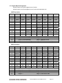
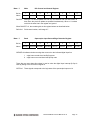
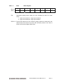
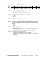
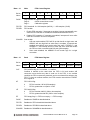
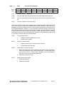
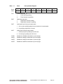
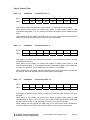
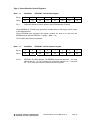
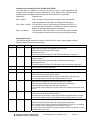
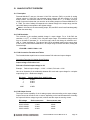
250 DIAMOND-MM-48-AT Autocalibrating 16-bit Analog I/O PC/104 Module With Relays and Optocouplers User Manual V1.01 Copyright 2004 Diamond Systems Corporation 8430-D Central Ave. Newark, CA 94560 Tel (510) 456-7800 www.diamondsystems.com TABLE OF CONTENTS 1. DESCRIPTION.......................................................................................................................... 3 2. DIAMOND-MM-48-AT BOARD DRAWING ............................................................................. 4 3. I/O HEADER PINOUT AND PIN DESCRIPTION..................................................................... 5 4. BOARD CONFIGURATION ..................................................................................................... 7 5. I/O MAP .................................................................................................................................... 9 6. REGISTER DEFINITIONS...................................................................................................... 11 7. ANALOG INPUT RANGES AND RESOLUTION .................................................................. 27 8. PERFORMING AN A/D CONVERSION................................................................................. 28 9. A/D SCAN, FIFO, AND INTERRUPT OPERATION .............................................................. 31 10. ANALOG OUTPUT OVERVIEW ............................................................................................ 34 11. GENERATING AN ANALOG OUTPUT ................................................................................. 35 12. AUTOCALIBRATION OPERATION ...................................................................................... 36 13. DIGITAL I/O OPERATION ..................................................................................................... 37 14. OPTOCOUPLER OPERATION.............................................................................................. 38 15. RELAY OPERATION ............................................................................................................. 40 16. COUNTER/TIMER OPERATION............................................................................................ 41 17. SPECIFICATIONS .................................................................................................................. 44 Diamond-MM-48-AT User Manual V1.01 Page 2 DIAMOND-MM-48-AT Autocalibrating Analog I/O PC/104 Module 1. DESCRIPTION Diamond-MM-48-AT (DMM-48-AT) is a PC/104 expansion board offering embedded systems designers a full feature set of analog and digital I/O capabilities. It is designed to be used in any PC-compatible embedded computer with a PC/104 (ISA-bus) expansion connector. DMM-48-AT offers reduced embedded system size and weight, as well as lower cost, by providing more functionality on one board than other data acquisition boards. Key features include: Analog Inputs ♦ 16 single-ended analog inputs ♦ 16-bit A/D resolution ♦ 200KHz maximum aggregate A/D sampling rate ♦ +/-10V and +/-5V input ranges standard; 0-5V input range optional ♦ 2048-sample FIFO for reliable high-speed sampling ♦ Autocalibrated input circuit Analog Outputs ♦ 8 analog outputs ♦ 12-bit D/A resolution, 0-4.096V output range (1mV per LSB) ♦ Autocalibrated output circuit Digital I/O ♦ 4 programmable direction digital I/O lines ♦ Edge detection capability with interrupt on change of state Optocoupler Inputs ♦ 4 optocoupler inputs, 3-28VDC input range ♦ Configurable input polarity ♦ Edge detection capability with interrupt on change of state Relay Outputs ♦ 8 SPDT (form C) relays ♦ 1A / 30VDC or 0.125A / 125VAC rating Counter/Timers ♦ 1 24-bit counter/timer for A/D sampling rate control ♦ 1 16-bit counter/timer for user counting and timing functions ♦ Programmable clock source for user counter/timer System Features ♦ +5V-only operation ♦ Latching I/O connectors ♦ Jumpers may be replaced with zero-ohm resistors for increased ruggedness ♦ Extended temperature operation (-40 to +85oC) Diamond-MM-48-AT User Manual V1.01 Page 3 2. DIAMOND-MM-48-AT BOARD DRAWING Feature descriptions J1 PC/104 8-bit bus connector J2 PC/104 16-bit bus connector J3 Analog and digital I/O connector J4 Relay and optocoupler I/O connector J6 Configuration jumper block J7 Factory use only (used in factory calibration process) J10 +/-5 input range selection (bipolar model only) Diamond-MM-48-AT User Manual V1.01 Page 4 3. I/O HEADER PINOUT AND PIN DESCRIPTION Diamond-MM-48-AT provides two I/O headers. J3, located on the right side of the board, is a 40-pin header that includes the analog in, analog out, and logic-level digital I/O features. Pin 1 is the upper left pin and is marked on the board. J4, located on the left side of the baord, is a 34-pin header with the relay and optocoupler features. J3: Analog and Digital I/O Vin 0 Vin 2 Vin 4 Vin 6 Vin 8 Vin 10 Vin 12 Vin 14 A/D Gnd Vout 0 Vout 2 Vout 4 Vout 6 D/A Gnd Extclk Out 0 Gate 1 DIO 0 DIO 2 +5V Signal Name Vin 0-15 Vout 0-7 DIO 0-3 Extclk Gate 0 Out 0 Clk 1 Gate 1 Out 1 +5V A/D Gnd D/A Gnd Dgnd 1 3 5 7 9 11 13 15 17 19 21 23 25 27 29 31 33 35 37 39 2 4 6 8 10 12 14 16 18 20 22 24 26 28 30 32 34 36 38 40 Vin 1 Vin 3 Vin 5 Vin 7 Vin 9 Vin 11 Vin 13 Vin 15 A/D Gnd Vout 1 Vout 3 Vout 5 Vout 7 Dgnd Gate 0 Clk 1 Out 1 DIO 1 DIO 3 Dgnd Definition Analog input channels 0 to 15; all inputs are single-ended Analog output channels 0 – 7 Digital I/O port, TTL / CMOS compatible; programmable direction External A/D trigger input Counter 0 gate input Counter 0 output Counter 1 clock input Counter 1 gate input Counter 1 output Connected to PC/104 bus power supply Analog ground for analog inputs Analog ground for analog outputs Digital ground Note: all grounds are electrically connected. The different pins are intended to reduce noise by separating the current paths on the board. Diamond-MM-48-AT User Manual V1.01 Page 5 J4: Relays and Optocouplers Opto 0Opto 1Opto 2Opto 3No connection Relay 0 NO Relay 0 C Relay 1 NC Relay 2 NO Relay 2 C Relay 3 NC Relay 4 NO Relay 4 C Relay 5 NC Relay 6 NO Relay 6 C Relay 7 NC Signal Name 1 3 5 7 9 11 13 15 17 19 21 23 25 27 29 31 33 2 4 6 8 10 12 14 16 18 20 22 24 26 28 30 32 34 Opto 0+ Opto 1+ Opto 2+ Opto 3+ No connection Relay 0 NC Relay 1 NO Relay 1 C Relay 2 NC Relay 3 NO Relay 3 C Relay 4 NC Relay 5 NO Relay 5 C Relay 6 NC Relay 7 NO Relay 7 C Definition Relay output contacts: Relay N C Relay N NC Relay N NO (N = 0 to 7) Relay output common contact; this contact is always used with relay output connections. Relay output normally connected contact; this contact is connected to the Out N C contact when power is off or when a 0 is written to the relay’s control bit in the relay control register, and it is disconnected when power is on and a 1 is written to the relay’s control bit. Relay output normally open contact; this contact is disconnected when power is off or when a 0 is written to the relay’s control bit in the relay control register, and it is connected to the Out N C contact when power is on and a 1 is written to the relay’s control bit. Optoisolated input contacts: Opto N + Opto N - (N = 0 to 3) Optoisolated input contact, high side Optoisolated input contact, low side; opto inputs are polarized Diamond-MM-48-AT User Manual V1.01 Page 6 4. BOARD CONFIGURATION Refer to the Drawing of Diamond-MM-48-AT on page 4 for locations of the configuration items mentioned here. All configuration except the A/D input range is done with jumper block J6. 4.1 Base Address Each board in your system must have a unique I/O address range. The first address in this range is called the base address. Diamond-MM-48-AT uses an I/O range of 16 bytes. The base address of this range is set with a portion of jumper block J6, located along the lower portion of the board near the PC/104 bus connectors. Each of the six jumper locations marked 10, 9, 8, 7, 6, 5 corresponds to the same-numbered address bit in the board’s 10-bit I/O address. Bits 4-0 are always 0 for the base address, resulting in a 16-byte I/O address block located on a 32-byte boundary. A jumper out is equal to a 1, and a jumper in is equal to a 0. Although any address is selectable, certain locations are reserved or may cause conflicts with other system resources. The table below lists recommended base address settings for Diamond-MM-48-AT. The default setting is 300 Hex. Base Address Hex 200 240 280 2C0 300 340 380 3C0 Decimal 512 512 512 512 768 (Default) 832 896 960 Jumper Position 10 In In In In In In In In 9 Out Out Out Out Out Out Out Out 8 In In In In Out Out Out Out 7 In In Out Out In In Out Out 6 In Out In Out In Out In Out 5 In In In In In In In In 4.2 Interrupt Level Selection In addition to the base address described above, J6 is used to configure hardware interrupt activity. Interrupts are used for several functions. They can be used to transfer A/D data from the board to memory at a rate higher than can be achieved through software sampling. In addition, they can be used to indicate to the application software when a change of state has occurred on the optocoupler or digital inputs. During interrupt operation, the board will periodically generate an interrupt request, or IRQ. The processor will respond and run a user-supplied interrupt routine function, or the function supplied with the board’s driver software. The interrupt routine reads the data from the board and makes it available to the user application program. DMM-48-AT allows you to select from levels 15, 14, 12, 11, 10, 9, 7, 6, 5, 4, and 3. Only one IRQ level may be used. To select the desired IRQ level install a jumper in that number’s location in the Interrupt area of jumper block J6. On the PC/104 bus each IRQ level in use must have a 1KΩ pull-down resistor attached. To enable the pull-down resistor for this board, install a jumper in the R location on J6. Typically each board in the computer will use a different interrupt level, or IRQ level. However in special circumstances multiple boards may share the same IRQ level. In this case only one Diamond-MM-48-AT User Manual V1.01 Page 7 board should have the pull-down resistor enabled with a jumper in the R location. The other boards should have the R jumper removed to disable their pull-down resistors. 4.3 Optocoupler Polarity The 4 optocouplers may be configured for either direct or inverted polarity with the POL position on J6. For direct polarity, an open circuit / low voltage input reads back as a 0, and a high voltage reads back as a 1. For inverted polarity, an open circuit / low voltage reads as 1, and a high voltage reads as 0. For direct polarity, the POL jumper should be absent. For inverted polarity, install a jumper in the POL location. 4.4 Reserved The EWP position on J6 is reserved for a future option and currently has no function. 4.5 Analog Input Range On the standard bipolar input range model, the input range can be selected with a jumper for either +/-10V or +/-5V. For +/-10V operation, jumper block J10 should be open. For +/-5V operation, install a jumper in J10. On the unipolar input range model, the input range is fixed at 0-5V, and J10 does not serve any purpose. Diamond-MM-48-AT User Manual V1.01 Page 8 5. I/O MAP 5.1 Overview Diamond-MM-48-AT occupies 16 bytes in I/O memory space. A functional list of these registers is provided below, and detailed register bit definitions are provided on the next page and the following chapter. The information in chapters 5 and 6 is provided to assist in understanding the board’s operation and for use by programmers writing their own driver software. Diamond Systems’ Universal Driver software provides high-level control of the board’s functionality and will isolate these underlying hardware details for most programmers. Base + 0 1 2 3 4 5 6 7 8 9 10 11 Write Function D/A LSB D/A MSB A/D channel register Relay control register Digital I/O configuration Digital I/O output data Optocoupler configuration D/A channel and update control Command register Configuration register FIFO control register Interrupt control register Read Function A/D LSB A/D MSB A/D channel register Relay control readback Digital I/O config + status readback Digital I/O input and edge data Optocoupler configuration readback Optocoupler input and edge data Status register Configuration register readback FIFO status register Interrupt status register Addresses 12-15 form a window into 2 4-byte pages. The page is selected with a bit in register 10. Page 0: counter/timers 12 Ctr 0 and Ctr 1 LSB 13 Ctr 0 CSB (center byte) / Ctr 1 MSB 14 Ctr 1 MSB 15 Counter/timer control register Ctr 0 and Ctr 1 MSB Ctr 0 CSB / Ctr 1 MSB Ctr 1 MSB --- Page 1: Calibration Control 12 EEPROM / TrimDAC data register 13 EEPROM / TrimDAC address register 14 Calibration control register 15 EEPROM access key EEPROM / TrimDAC data register EEPROM / TrimDAC address register Calibration status register FPGA code version Diamond-MM-48-AT User Manual V1.01 Page 9 5.2 Register Map Bit Assignments A blank location in the Write registers has no function. A blank location in the Read registers has no function and reads back as 0. WRITE operations 0 7 6 5 4 3 2 1 0 DA7 DA6 DA5 DA4 DA3 DA2 DA1 DA0 DA11 DA10 DA9 DA8 1 2 HIGH3 HIGH2 HIGH1 HIGH0 LOW3 LOW2 LOW1 LOW0 3 RELAY7 RELAY6 RELAY5 RELAY4 RELAY3 RELAY2 RELAY1 RELAY0 4 DIR3 DIR2 DIR1 DIR0 5 DIO3 DIO2 DIO1 DIO0 POL3 POL2 POL1 POL0 DAUPDT DACH2 DACH1 DACH0 DAPRE DAPRLD RESET CKFRQ1 CKFRQ0 SCNINT CLKEN CLKSEL PAGE FIFOTH FIFOEN SCANEN TINTE DINTE OINTE AINTE 6 OEN3 OEN2 OEN1 OEN0 7 8 9 CKSEL1 10 11 CLRT CLRD CLRO CLRA FIFORST ADSTART 12 Page 0: Counter data LSB Page 1: Calibration Data 13 Page 0: Counter data CSB Page 1: Calibration Address 14 Page 0: Counter data MSB Page 1: Calibration Control 15 Page 0: Counter Control Register Page 1: EEPROM Access Key Register READ operations 0 7 6 5 4 3 2 1 0 AD7 AD6 AD5 AD4 AD3 AD2 AD1 AD0 1 AD15 AD14 AD13 AD12 AD11 AD10 AD9 AD8 2 HIGH3 HIGH2 HIGH1 HIGH0 LOW3 LOW2 LOW1 LOW0 3 RELAY7 RELAY6 RELAY5 RELAY4 RELAY3 RELAY2 RELAY1 RELAY0 DIR3 DIR2 DIR1 DIR0 4 5 DEDGE3 DEDGE2 DEDGE1 DEDGE0 DIO3 DIO2 DIO1 DIO0 6 OEN3 OEN2 OEN1 OEN0 POL3 POL2 POL1 POL0 7 OEDGE3 OEDGE2 OEDGE1 OEDGE0 OPTO3 OPTO2 OPTO1 OPTO0 POL ADCH3 ADCH2 ADCH1 ADCH0 8 9 ADBUSY DABUSY CKSEL1 CKFRQ1 CKFRQ0 SCNINT CLKEN CLKSEL 10 OVF HF 8F EF PAGE FIFOTH FIFOEN SCANEN 11 TINT DINT OINT AINT TINTE DINTE OINTE AINTE 12 Page 0: Counter data LSB Page 1: Calibration Data 13 Page 0: Counter data CSB Page 1: Calibration Address 14 Page 0: Counter data MSB Page 1: Calibration Control/Status 15 Page 0: --- Page 1: FPGA revision code Diamond-MM-48-AT User Manual V1.01 Page 10 6. REGISTER DEFINITIONS Base + 0 Write D/A LSB Bit No. 7 6 5 4 3 2 1 0 Name DA7 DA6 DA5 DA4 DA3 DA2 DA1 DA0 Definitions: DA7-0 Base + 0 D/A bits 7-0; DA0 is the LSB. D/A data is an unsigned 12-bit number ranging from 0 to 4095. Read A/D LSB Bit No. 7 6 5 4 3 2 1 0 Name AD7 AD6 AD5 AD4 AD3 AD2 AD1 AD0 Definitions: AD7 – 0 Base + 1 A/D LSB data (bits 7-0 of the 16-bit value). A/D data is a signed 16-bit value ranging from -32768 to 32767. Write Bit No. 7 Name DAC 0 – 3 MSB 6 5 4 3 2 1 0 DA11 DA10 DA9 DA8 Definitions: DA11 – 8 D/A data bits 11-8 for the selected channel. DA11 is the MSB. Diamond-MM-48-AT User Manual V1.01 Page 11 Base + 1 Read A/D MSB Bit No. 7 6 5 4 3 2 1 0 Name AD15 AD14 AD13 AD12 AD11 AD10 AD9 AD8 Definitions: AD15 – 8 A/D MSB data (bits 15-8 of the 16-bit value). A/D data is a signed 16-bit value ranging from -32768 to 32767. Note: Reading from Base + 0 and Base + 1 result in the same physical operation, reading from the FIFO. The FIFO is 8 bits wide x 2048 bytes deep, with A/D data stored and retrieved in interleaved fashion. Data from the A/D is put into the FIFO in little-endian mode, with the LSB inserted first, and the MSB inserted second. Thus the data comes out of the FIFO in the same order. Each time a byte is read from either Base + 0 or Base + 1, the next byte will be read from the FIFO and the FIFO counter will be decremented. Because the FIFO decrements after each read operation, you cannot read out the same A/D value more than once (unless the FIFO is empty, in which case the last byte may be read indefinitely). It is the programmer’s responsibility to ensure that data is read out of the FIFO properly so that appropriate LSB / MSB pairs are read out together. Base + 2 Read/Write A/D Channel Register Bit No. 7 6 5 4 3 2 1 0 Name HIGH3 HIGH2 HIGH1 HIGH0 LOW3 LOW2 LOW1 LOW0 Definitions: HIGH3 – 0 High channel of channel scan range; ranges from LOW to 15 LOW3 – 0 Low channel of channel scan range; ranges from 0 to 15 The high channel must be greater than or equal to the low channel. When this register is written, the current A/D channel is set to the low channel and ADBUSY = 1 for 10 uS. A/D channels are automatically selected in sequence by the board. Each time an A/D conversion starts, the board increments to the next channel in the range. When the high channel is sampled, the board resets to the low channel. Diamond-MM-48-AT User Manual V1.01 Page 12 Base + 3 Read/Write Relay Control Port Bit No. 7 6 5 4 3 2 1 0 Name RELAY7 RELAY6 RELAY5 RELAY4 RELAY3 RELAY2 RELAY1 RELAY0 These bits control the 8 relays. 0 = off (C connected to NC), 1 = on (C connected to NO). The written value may be read back with true logic. The value on the corresponding output pin is the inverse of the value in this register. On power-up or reset, the output register is cleared to all zeroes and all relays reset to their off condition (C connected to NC) by resetting all RELAY pins to 1. Relays are in the off condition when power is off and remain in that condition when power is applied until a 1 is written to their corresponding control register bit. Base + 4 Read/Write Bit No. 7 Digital I/O Configuration Register 6 5 4 Name 3 2 1 0 DIR3 DIR2 DIR1 DIR0 Definitions: DIR3-0 Digital I/O direction settings for each bit: 1 = output, 0 = input All digital I/O lines are in input mode on power-up. Diamond-MM-48-AT User Manual V1.01 Page 13 Base + 5 Write Bit No. Digital I/O Data 7 6 5 4 Name 3 2 1 0 DIO3 DIO2 DIO1 DIO0 Definitions: DIO3 – 0 Base + 5 Digital I/O output data. Only bits in output mode are affected. Any bit in input mode will ignore data written to this register. Read Bit No. Name Digital I/O Data and Edge Status 7 6 5 4 DEDGE3 DEDGE2 DEDGE1 DEDGE0 3 2 1 0 DIO3 DIO2 DIO1 DIO0 Definitions: DEDGE3 – 0 Edge status for DIO lines: 1 = change occurred since last read, 0 = no change occurred DIO3 – 0 Base + 6 Digital I/O readback. If a bit is in output mode, the readback value is equal to the programmed value. Read/Write Optocoupler Edge Detection Configuration Register Bit No. 7 6 5 4 3 2 1 0 Name OEN3 OEN2 OEN1 OEN0 POL3 POL2 POL1 POL0 OEN3-0 Enable edge detection on the selected digital input line: 0 = disabled, 1 = enabled POL3-0 Select active edge polarity for selected digital input line: 0 = falling, 1 = rising An interrupt request will occur when OINTE = 1 and a digital input line enabled with OENn exhibits an edge whose polarity matches POLn (a qualifying edge). If an interrupt request occurs, and an additional qualifying edge occurs before the digital interrupt flip flop is reset, no additional interrupt request will be generated. It is possible for more than one line’s qualifying edge to be detected in a single interrupt (for example if 3 lines exhibit qualifying edges at the same time), but not more than one edge per line (for example if a second qualifying edge on the same line occurs before the interrupt is serviced). It is possible for a qualifying edge to occur in the time between when the interrupt routine reads the digital input status register and when it resets the interrupt flip flop. In this case the qualifying edge will be lost, since resetting the flip flop also resets the edge detection status bits. Diamond-MM-48-AT User Manual V1.01 Page 14 Base + 7 Write Bit No. 7 D/A Channel and Control Register 6 5 4 Name DAUPDT 3 2 1 0 DAUPDT DACH2 DACH1 DACH0 Writing a 1 to this bit updates the D/A chip. All channels with new data written to them since the previous update are updated simultaneously. When a 1 is written to this bit the other bits in the register are ignored. When DAUPDT = 0, the remaining bits in this register behave as described below: DACH2-0 Base + 7 Read Bit No. Name D/A channel number, valid range 0-7 7 Optocoupler Input Port and Edge Detection Register 6 5 4 OEDGE3 OEDGE2 OEDGE1 OEDGE0 3 2 1 0 OPTO3 OPTO2 OPTO1 OPTO0 OEDGE3-0 Indicates whether an edge has occurred on the indicated digital input line. 1 edge has occurred since last flip flop reset 0 edge has not occurred since last flip flop reset These bits are reset when this register is read or when the digital input interrupt flip flop is reset by writing to the CLRO bit in register 8. OPTO3-0 These signals correspond to the logic state of the optocoupler inputs on J4. Diamond-MM-48-AT User Manual V1.01 Page 15 Base + 8 Bit No. Write 7 Command Register 6 5 Name 4 3 2 DAPRE DAPRLD RESET 1 0 FIFORST ADSTART Writing a 1 to any bit in this register causes a command or operation to be executed. Only one bit may be activated (set to 1) at a time. When a 1 is written to any bit, no other bit or related operation is affected. DAPRE All 8 D/A channels are set to the value in the D/A preset register. This value is user-definable and can be used for any purpose. A typical purpose is to generate a D/A reset to 0V by loading a preset value that corresponds to 0V for the selected D/A mode. For example, for D/A in unipolar mode, the preset value would be 0, and for D/A in bipolar mode, the preset value would be 2048. DAPRLD The D/A preset register is loaded with the value contained in registers 0-1. After the preset value is loaded into the D/A, a DAPRE command will update all 8 D/A channels with this value. RESET Reset the board to a known condition: All registers are cleared to 0, all DIO lines are set to input mode, interrupts are disabled, and the FIFO is reset. D/A channels are not reset or changed in any way. FIFORST Reset FIFO. Writing a 1 to this bit causes the on-board FIFO to be reset to empty in preparation for an interrupt-based A/D operation. After FIFORST, EF = 1 and OVF, FF, and HF = 0. ADSTART Start an A/D conversion. Diamond-MM-48-AT User Manual V1.01 Page 16 Base + 8 Bit No. Name POL Read 7 Status Register 6 5 4 3 2 1 0 POL ADCH3 ADCH2 ADCH1 ADCH0 Optocoupler polarity jumper setting; the value indicates the value of an open circuit: 1 Open circuit reads as 1, “high” input reads as 0 0 Open circuit reads as 0, “high” input reads as 1 ADCH3 - 0 Current A/D channel; this is the channel currently selected on board and is the channel that will be used for the next A/D conversion (unless a new value is written to the channel register before then). Diamond-MM-48-AT User Manual V1.01 Page 17 Base + 9 Bit No. Name Write 7 Configuration Register 6 5 CKSEL1 4 3 CKFRQ1 CKFRQ0 2 1 0 SCNINT CLKEN CLKSEL CKSEL1 Clock source select for counter/timer 1: 1 External signal Clk0 in I/O connector J3 0 On-board clock, frequency selected by CKFRQ1 below CKFRQ1 Clock frequency select for counter/timer 1 when CKSEL1 = 0: 1 100KHz 0 10MHz CKFRQ0 Clock frequency select for counter/timer 0: 1 1MHz 0 10MHz SCNINT Scan interval. This is the time between A/D samples during an A/D scan. An A/D scan occurs when SCANEN = 1 (Base + 10 bit 4) and an A/D conversion is triggered. 1 5.0µS 0 9.3µS CLKEN Enable hardware A/D clock: 1 Enable hardware A/D trigger (source is selected with CLKSEL bit); software triggers are disabled 0 Disable hardware trigger; A/D is triggered by setting the ADSTART bit CLKSEL A/D clock select, used only when CLKEN = 1: 1 Internal clock: counter/timer 0 generates A/D conversions 0 External clock: the EXTCLK pin on I/O connector J3, generates A/D conversions Diamond-MM-48-AT User Manual V1.01 Page 18 Base + 9 Read Bit No. Name 7 Configuration & Status Register 6 ADBUSY DABUSY ADBUSY 5 CKSEL1 4 3 CKFRQ1 CKFRQ0 2 1 0 SCNINT CLKEN CLKSEL A/D chip status: 1 A/D conversion or scan is in progress or A/D input circuit in settling mode 0 A/D is idle Do not attempt to start a new A/D conversion or scan when ADBUSY = 1. DABUSY D/A chip status: 1 D/A conversion is in progress 0 D/A is idle Do not attempt to start a new D/A conversion when DABUSY = 1. CKSEL1 Clock source select for counter/timer 1: 1 External signal Clk0 in I/O connector J3 0 On-board clock, frequency selected by CKFRQ1 below CKFRQ1 Clock frequency select for counter/timer 1 when CKSEL1 = 0: 1 100KHz 0 10MHz CKFRQ0 Clock frequency select for counter/timer 0: 1 1MHz 0 10MHz SCNINT Scan interval. This is the time between A/D samples during an A/D scan. An A/D scan occurs when SCANEN = 1 (Base + 10 bit 4) and an A/D conversion is triggered. 1 5.0µS 1 9.3µS CLKEN Enable hardware A/D clock: 1 Enable hardware A/D trigger (source is selected with CLKSEL bit); software triggers are disabled 0 Disable hardware trigger; A/D is triggered by setting the ADSTART bit CLKSEL A/D clock select, used only when CLKEN = 1: 1 Internal clock: counter/timer 0 generates A/D conversions 0 External clock: the EXTCLK pin on I/O connector J3, generates A/D conversions Diamond-MM-48-AT User Manual V1.01 Page 19 Base + 10 Bit No. Write 7 FIFO Control Register 6 5 4 Name 3 2 1 0 PAGE FIFOTH FIFOEN SCANEN PAGE Page number for registers at Base + 12 through Base + 15 Page 0: 82C54 counter/timer access Page 1: Calibration registers FIFOTH FIFO threshold: 0 = 1024 samples (half full), 1 = 256 samples (1/8 full) FIFOEN FIFO enable: 1 Enable FIFO operation; if interrupts are enabled, interrupt requests will occur when the FIFO reaches or exceeds the threshold selected with FIFOTH. 0 Disable FIFO operation; if interrupts are enabled, interrupts will occur after each A/D conversion or scan is completed. SCANEN Scan enable: 1 A/D scan mode enabled; FIFO will fill up with data for a single scan, and ADBUSY will stay high until an entire scan is complete. If interrupts are enabled, interrupts will occur at the end of the scan. If FIFOEN = 1 and SCANEN = 1, the interrupt will occur at the end of the scan that causes the FIFO to reach or exceed its half-full point (256 samples). 0 Scan mode disabled; the ADBUSY bit will remain high for a single conversion Base + 10 Read FIFO Status Register Bit No. 7 6 5 4 3 2 1 0 Name OVF HF 8F EF PAGE FIFOTH FIFOEN SCANEN OVF FIFO overflow flag: 0 = no overflow, 1 = overflow Overflow is defined as the state when the FIFO is full and another A/D conversion occurs before any data is read out of the FIFO. In an overflow condition the FIFO contents are preserved, and no new data will be written to the FIFO. To clear an overflow condition, the FIFO must be reset with the FIFORST bit in register 8. 8F FIFO 1/8 full flag: 0 FIFO is less than 1/8 full (256 samples) 1 FIFO is greater than or equal to 1/8 full HF FIFO half full flag 0 FIFO is less than half full (1024 or less samples) 1 FIFO is greater than half full (1025 or more samples) EF FIFO empty flag: 0 = FIFO is not empty, 1 = FIFO is empty PAGE Readback of PAGE bit described above FIFOTH Readback of FIFO threshold bit described above FIFOEN Readback of FIFOEN bit described above SCANEN Readback of SCANEN bit described above Diamond-MM-48-AT User Manual V1.01 Page 20 Base + 11 Write Interrupt Control Register Bit No. 7 6 5 4 3 2 1 0 Name CLRT CLRD CLRO CLRA TINTE DINTE OINTE AINTE CLRT Clear the timer interrupt flip flop. CLRD Clear the digital input interrupt flip flop and reset their edge detect status bits. CLRO Clear the optocoupler input interrupt flip flop and reset their edge detect status bits. CLRA Clear the analog input interrupt flip flop. The interrupt flip flop for each circuit is set whenever an interrupt request is generated by that circuit, and it must be cleared by software before another interrupt of that type can be generated. An interrupt request from one or more circuits will generate an interrupt request on the selected IRQ line. Writing a 1 to any CLRx bit clears the interrupt flip flop for that circuit and leaves alone all other bits in this register. Writing a 0 to a CLRx bit has no effect on that circuit. Each circuit’s interrupt flip flop can be reset individually. When all interrupt circuits have been reset, either by clearing them individually or by disabling them with xINTE = 0, the board’s interrupt request line will be tristated. TINTE DINTE OINTE AINTE Timer interrupt enable: 1 Enable interrupts on falling edge of timer 1 0 Disable timer interrupts Digital I/O interrupt enable: 1 Enable interrupts on any change of state of DIO3-0 0 Disable digital input interrupts Optocoupler input interrupt enable: 1 Enable optocoupler interrupts on change of state determined by register 6; in order for an interrupt to occur, OINTE must be set to 1, at least one of OEN30 must also be set to 1, and the edge indicated by the corresponding bit POL3-0 must occur on the selected optocoupler. 0 Disable optocoupler interrupts Analog input interrupt enable: 1 Enable A/D interrupts 0 Disable A/D interrupts Diamond-MM-48-AT User Manual V1.01 Page 21 Base + 11 Read Interrupt Status Register Bit No. 7 6 5 4 3 2 1 0 Name TINT DINT OINT AINT TINTE DINTE OINTE AINTE TINT Timer interrupt status: 1 Timer interrupt pending 0 Timer interrupt not pending DINT Digital interrupt status: 1 Digital input interrupt pending 0 Digital input interrupt not pending OINT Optocoupler input interrupt request status: AINT 1 One or more qualifying edges have occurred on the optocouplers 0 No qualifying edges have occurred Analog input interrupt request status: 1 Interrupt request is pending from A/D circuit 0 No interrupt is pending from A/D circuit TINTE Readback of TINTE bit described on previous page DINTE Readback of DINTE bit described on previous page OINTE Readback of OINTE bit described on previous page AINTE Readback of AINTE bit described on previous page Diamond-MM-48-AT User Manual V1.01 Page 22 Page 0: Counter/Timer Base + 12 Read/Write Counter/Timer D7 - 0 Bit No. 7 6 5 4 3 2 1 0 Name D7 D6 D5 D4 D3 D2 D1 D0 This register is used for both Counter 0 and Counter 1. It is the LSB for both counters. When writing to this register, an internal load register is loaded. Upon issuing a Load command through Base + 15, the selected counter’s LSB register will be loaded with this value. When reading from this register, the LSB value of the most recent Latch command will be returned. The value returned is NOT the value written to this register. Base + 13 Read/Write Counter/Timer D15 - 8 Bit No. 7 6 5 4 3 2 1 0 Name D15 D14 D13 D12 D11 D10 D9 D8 This register is used for both Counter 0 and Counter 1. It is the MSB for counter 1 and the middle byte for counter 0. When writing to this register, an internal load register is loaded. Upon issuing a Load command through Base + 15, the selected counter’s associated register will be loaded with this value. For counter 0, it is the middle byte. For counter 1, it is the MSB. When reading from this register, the associated byte of the most recent Latch command will be returned. The value returned is NOT the value written to this register. Base + 14 Read/Write Counter/Timer D23 - 16 Bit No. 7 6 5 4 3 2 1 0 Name D23 D22 D21 D20 D19 D18 D17 D16 This register is used for Counter 0 only. Counter 0 is 24 bits wide, while Counter 1 is only 16 bits wide. When writing to this register, an internal load register is loaded. Upon issuing a Load command through Base + 15 for Counter 0, the counter’s MSB register will be loaded with this value. When issuing a Load command for counter 1, this register is ignored. When reading from this register, the MSB value of the most recent Latch command for counter 0 will be returned. The value returned is NOT the value written to this register. Diamond-MM-48-AT User Manual V1.01 Page 23 Base + 15 Write Counter/Timer Control Register Bit No. 7 6 5 4 3 2 1 0 Name CTRNO LATCH GTDIS GTEN CTDIS CTEN LOAD CLR This register is used to control the counter/timers. A counter is selected with bit 7, and then a 1 is written to any ONE of bits 6 – 0 to select the desired operation for that counter. The other bits and associated functions are not affected. Thus only one operation can be performed at a time. CTRNO Counter no., 0 or 1 LATCH Latch the selected counter so that its value may be read. The counter must be latched before it is read. Reading from registers 12-14 returns the most recently latched value. If you are reading Counter 1 data, read only Base + 12 and Base + 13. Any data in Base + 14 will be from the previous Counter 0 access. GTDIS Disable external gating for the selected counter. GTEN Enable external gating for the selected counter. If enabled, the associated gate signal GATE0 or GATE1 controls counting on the counter. If the GATEn signal is high, counting is enabled. If the GATEn signal is low, counting is disabled. CTDIS Disable counting on the selected counter. The counter will ignore input pulses. CTEN Enable counting on the selected counter. The counter will decrement on each input pulse. LOAD Load the selected counter with the data written to Base + 12 through Base + 14 or Base + 12 and Base + 13 (depending on which counter is being loaded). CLR Clear the current counter (set its value to 0). To load a counter: First write the load value to Base + 12 and Base + 13 (for Counter 1) or Base + 12 through Base + 14 (for Counter 0). Then write a Load command to Base + 15. For example, to load Counter 0 with the hex value 123456: ♦ Write 0x12 to Base + 14 (these three bytes can be written to in any order) ♦ Write 0x34 to Base + 13 ♦ Write 0x56 to Base + 12 ♦ Write 0x02 to Base + 15 to load counter 0 To enable counting: Write 0x04 (ctr 0) or 0x84 (ctr 1) to Base + 15. To stop counting: Write 0x08 (ctr 0) or 0x88 (ctr 1) to Base + 15. To read a counter: First latch it, then read the value: ♦ Write 0x40 to Base + 15 to latch counter 0 or 0xC0 to latch counter 1 ♦ Read LSB from Base +12 ♦ Read Middle Byte from Base + 13 ♦ Read MSB from Base + 14 ♦ Assemble 3 bytes into the current counter value Diamond-MM-48-AT User Manual V1.01 Page 24 Page 1: Autocalibration Control Registers Base + 12 Read/Write EEPROM / TrimDAC Data Register Bit No. 7 6 5 4 3 2 1 0 Name D7 D6 D5 D4 D3 D2 D1 D0 D7-0 Calibration data to be read or written to the EEPROM and/or TrimDAC. During EEPROM or TrimDAC write operations, the data written to this register will be written to the selected device. During EEPROM read operations this register contains the data to be read from the EEPROM and is valid after EEBUSY = 0 (Page 1, Base + 14). The TrimDAC data cannot be read back. Base + 13 Read/Write EEPROM / TrimDAC Address Register Bit No. 7 6 5 4 3 2 1 0 Name A7 A6 A5 A4 A3 A2 A1 A0 A7-A0 EEPROM / TrimDAC address. The EEPROM recognizes address 0 – 127 using address bits A6 – A0. The TrimDAC only recognizes addresses 0 – 7 using bits A2 – A0. In each case remaining address bits will be ignored. Diamond-MM-48-AT User Manual V1.01 Page 25 Base + 14 Write Calibration Control Register Bit No. 7 6 5 Name EE_EN EE_RW 4 3 2 1 0 RUNCAL CMUXEN TDACEN This register is used to initiate various commands related to autocalibration. More detailed information on autocalibration may be found elsewhere in this manual. EE_EN EEPROM Enable. Writing a 1 to this bit will initiate a transfer to/from the EEPROM as indicated by the EE_RW bit. EE_RW Selects read or write operation for the EEPROM: 0 = Write, 1 = Read. RUNCAL Writing 1 to this bit causes the board to reload the calibration settings from EEPROM. CMUXEN Calibration multiplexor enable. The cal mux is used to read precision on-board reference voltages that are used in the autocalibration process. It also can be used to read back the value of analog output 0. 1 = enable cal mux and disable user analog input channels 0 = disable cal mux, enable user inputs TDACEN Base + 14 TrimDAC Enable. Writing 1 to this bit will initiate a transfer to the TrimDAC (used in the autocalibration process). Read Bit No. 7 Name 0 TDBUSY EEBUSY Base + 15 Calibration Status Register 6 5 4 3 TDBUSY EEBUSY CMUXEN TDACEN 2 1 0 0 0 0 TrimDAC busy indicator 0 User may access TrimDAC 1 TrimDAC is being accessed; user must wait EEPROM busy indicator 0 User may access EEPROM 1 EEPROM is being accessed; user must wait Write EEPROM Access Key Register The user must write the value 0xA5 (binary 10100101) to this register each time after setting the PAGE bit in order to get access to the EEPROM. This helps prevent accidental corruption of the EEPROM contents. Base + 15 Read FPGA Revision Code This register may be read back to indicate the revision level of the FPGA code. The FPGA revision starts at 1 and increments up each time the code is revised. Diamond-MM-48-AT User Manual V1.01 Page 26 7. ANALOG INPUT RANGES AND RESOLUTION 7.1 Resolution Diamond-MM-48-AT uses a 16-bit A/D converter. This means that the analog input voltage can be measured to the precision of a 16-bit binary number. The maximum value of a 16-bit binary number is 216 - 1, or 65535, so the full range of numerical values that you can get from a Diamond-MM-48-AT analog input channel is 0 - 65535. The smallest change in input voltage that can be detected is 1/(216), or 1/65536, of the fullscale input range. This smallest change results in an increase or decrease of 1 in the A/D code, and so this change is referred to as 1 LSB, or 1 least significant bit. 7.2 Input Ranges Diamond-MM-48-AT is available in two models. The default model has bipolar inputs of +/10V and +/-5V, selectable with jumper block J10. An optional model with a slightly different component configuration has unipolar inputs of 0-5V. 7.3 Single Ended and Differential Inputs A single-ended input is a two-wire input (one input signal and ground) that is referenced to analog ground on the board. This means that the input voltage will be measured with respect to the board’s analog ground. A differential input is a three-wire input (input +, input -, and ground), and the board will measure the difference between the voltages of the two inputs. Diamond-MM-48-AT works only with single-ended inputs. In some cases, a differential input can be simulated by connecting the high and low input wires to two adjacent analog input channels, measuring both of them with and A/D scan operation, and subtracting the low reading from the high reading. This will work only for very slow changing (or DC) signals with very low noise. The problem with this technique is that the two signals are sampled at different times, either 5µs or 9.3µs apart depending on the setting of the SCANINT register bit. This time delay can lead to measurement errors due to the change in the input signal during the delay. For example, an input signal consisting of a 1KHz sine wave with 10V amplitude has a maximum slope of 10V x 2 x π x 1000Hz = 63,000 V/sec, or 63 mV/µs. This represents a change of 315mV during the 5µs delay between the sampling of the high input and the low input. For a 16-bit A/D converter on a +/-10V input range, this is an error of over 1,000 counts. Diamond-MM-48-AT User Manual V1.01 Page 27 8. PERFORMING AN A/D CONVERSION This chapter describes the steps involved in performing an A/D conversion on a selected input channel using direct programming (not with the driver software). This describes the basic operation of a single A/D conversion without interrupts. For a more complete description including interrupts and all register control bits, see chapter 9. There are five steps involved in performing an A/D conversion: 1. Select the input channel 2. Wait for analog input circuit to settle 3. Trigger an A/D conversion 4. Wait for the conversion to finish 5. Read the data from the board 6. Convert the numerical data to a meaningful value 8.1 Select the input channel To select the input channel to read, write a low-channel/high-channel pair to the channel register at base + 2. (See Chapter 6). The low 4 bits select the low channel, and the high 4 bits select the high channel. When you write any value to this register, the current A/D channel is set to the low channel. For example: To set the board to channel 4 only, write 0x44 to Base + 2. To set the board to read channels 0 through 15, write 0xF0 to Base + 2. ⇒ Note: When you perform an A/D conversion, the current channel is automatically incremented to the next channel in the selected range. Therefore, to perform A/D conversions on a group of consecutively-numbered channels, you do not need to write the input channel prior to each conversion. For example, to read from channels 0 - 2, write Hex 20 to base + 2. The first conversion is on channel 0, the second will be on channel 1, and the third will be on channel 2. Then the channel counter wraps around to the beginning again, so the fourth conversion will be on channel 0 again, and so on. If you are sampling the same channel repeatedly, then you set both high and low to the same value as in the first example above. Then on subsequent conversions you do not need to set the channel again. 8.2 Wait for analog input circuit to settle After writing to the channel register (Base + 2), you must allow time for the analog input circuit to settle before starting an A/D conversion. The board has a built-in 10µs timer to assist with the wait period. Monitor the ADBUSY bit at Base + 9 bit 7. When it is 1 the circuit is actively settling on the input signal, or else the board is currently performing and A/D conversion or scan. When it is 0 the board is ready to perform A/D conversions. Diamond-MM-48-AT User Manual V1.01 Page 28 8.3 Trigger an A/D conversion on the current channel After the above steps are completed, start the A/D conversion by writing a 1 to the ADSTART bit in Base + 8. This write operation only triggers the A/D if the CLKEN bit is 0 to disable hardware triggering and enable software triggering. Otherwise the A/D will only trigger when the selected clock or trigger signal occurs. CLKEN should always be 0 when controlling A/D conversions in software. 8.4 Wait for the conversion to finish The A/D converter takes up to 5 microseconds to complete a conversion. Most processors and software can operate fast enough so that if you try to read the A/D converter immediately after writing to base + 0, you will beat the A/D converter and get invalid data. Therefore the A/D converter provides a status signal ADBUSY to indicate whether it is busy or idle. This bit can be read back as bit 7 in the status register at Base + 9. When the A/D converter is busy (performing an A/D conversion), this bit is 1, and when the A/D converter is idle (conversion is done and data is available), this bit is 0. Here is a pseudocode explanation: Status = read(base+9) AND 128 // or Status = read(base+9) AND 80 Hex If Status = 0 then conversion is complete, else A/D converter is busy Keep repeating this procedure until Status = 0. 8.5 Read the data from the board Once the conversion is complete, you can read the data back from the A/D converter. The data is 16 bits wide and is read back in two 8-bit bytes. The following pseudocode illustrates how to construct the 16-bit A/D value from these two bytes: LSB = read(base) MSB = read(base+1) Data = MSB * 256 + LSB // combine the 2 bytes into a 16-bit value The final data is interpreted as a signed value ranging from –32768 to +32767. ⇒ Note: The data range always includes both positive and negative values, even if the board is set to a unipolar input range. The data must now be converted to volts or other engineering units by using a conversion formula as shown on the next page. Diamond-MM-48-AT User Manual V1.01 Page 29 8.6 Convert the numerical data to a meaningful value Once you have the A/D code, you need to convert it to a meaningful value. The first step is to convert it back to the actual measured voltage. Afterwards you may need to convert the voltage to some other engineering units (for example, the voltage may come from a temperature sensor, and then you would need to convert the voltage to the corresponding temperature according to the temperature sensor’s characteristics). Since there are a large number of possible input devices, this secondary step is not included here; only conversion to input voltage is described. It is possible to combine both transformations into a single formula for computing efficiency. To convert the A/D value to the corresponding input voltage, use the following formulas: Conversion Formula for Bipolar Input Ranges Input voltage = A/D value / 32768 * Full-scale voltage Example: Input range is ±10V and A/D value is 17761: Input voltage = 17761 / 32768 * 10V = 5.420V For a bipolar input range, 1 LSB = 1/32768 * Full-scale voltage. For the +/-10V range, 1 LSB = 305µV, and for the +/-5V range, 1 LSB = 153µV. Here is an illustration of the relationship between A/D code and input voltage for a bipolar input range (VFS = Full scale input voltage, 10V or 5V): A/D Code -32768 -32767 ... -1 0 1 ... 32767 Input voltage symbolic formula -VFS -VFS + 1 LSB ... -1 LSB 0 +1 LSB ... VFS - 1 LSB Input voltage for ±10V range -10.0000V -9.9997V ... -0.00032V 0.0000V 0.00032V ... 9.9997V Conversion Formula for Unipolar Input Range Input voltage = (A/D value + 32768) / 65536 * Full-scale voltage Example: Input range is 0-5V and A/D value is 17761: Input voltage = (17761 + 32768) / 65536 * 5V = 3.855V For a unipolar input range of 0-5V, 1 LSB = 1/65536 * 5V = 76µV. Here is an illustration of the relationship between A/D code and input voltage for a unipolar input range (VFS = Full scale input voltage): A/D Code -32768 -32767 ... -1 0 1 ... 32767 Input voltage symbolic formula 0V 1 LSB (VFS / 65536) ... VFS / 2 - 1 LSB VFS / 2 VFS / 2 + 1 LSB ... VFS - 1 LSB Input voltage for 0-5V range 0.0000V 0.000076V ... 2.4999V 2.5000V 2.5001V ... 4.9999V Diamond-MM-48-AT User Manual V1.01 Page 30 9. A/D SCAN, FIFO, AND INTERRUPT OPERATION This chapter describes in detail the interrupt performance of the A/D circuit under all conditions. The control bits FIFOEN (FIFO enable), FIFOTH (FIFO threshold), SCANEN (scan enable), SCNINT (scan interval), and AINTE (A/D interrupt enable) determine the behavior of the board during A/D conversions with interrupts. Control bits CLKEN and CLKSEL determine the source of the A/D trigger, either software, on-board counter/timer, or external signal. In all cases, at the end of an AD conversion A/D data is latched into the FIFO in an interleaved fashion, first LSB, then MSB. A/D Data is read out of the FIFO with 2 read operations, first Base + 0 (LSB) and then Base + 1 (MSB). When SCANEN = 1, each time an A/D trigger occurs, the board will perform an A/D conversion on all channels in the channel range. The time between A/D conversions is determined by the setting of the SCNINT bit. When SCANEN = 0, each time an A/D trigger occurs, the board will perform a single A/D conversion and then advance to the next channel and wait for the next trigger. During interrupt operation, if FIFOEN = 1, then the FIFO will fill up with data until it reaches or exceeds half-full (half-full = 256 samples), and then the interrupt request will occur. The basic sequence is as follows: 1. 2. 3. 4. 5. A/D trigger command occurs A/D conversion or A/D scan occurs A/D data is stored in the FIFO Interrupt request occurs Interrupt routine extracts data from the FIFO and resets the interrup request A/D Trigger The A/D trigger may come from one of three sources as determined by the control bits CLKEN and CLKSEL: CLKEN CLKSEL 0 0 1 1 0 1 0 1 A/D trigger source Software command: write a 1 to ADSTART bit in register 8 Same as above External signal: rising edge on EXTCLK pin on I/O header J3 Internal; counter/timer 0 controls the A/D conversion timing A/D Conversion or Scan Once the A/D trigger occurs, either a single A/D conversion will occur on the current channel, or an A/D scan will occur on a range of channels selected by the setting of register 2. The selection is made with the control bit SCANEN: SCANEN Function 0 Single conversion occurs on the current channel; The internal A/D channel counter increments after each conversion, so each successive trigger samples the next channel in the list. At the end of the list, the channel register resets to the starting channel and the sequence repeats. 1 Scan occurs on all channels in the range programmed in the channel register (base + 2). The delay between the start of each conversion is determined by the setting of SCNINT in base + 9: SCNINT = 0 sets a delay of 5µs, and SCNINT = 1 sets a delay of 9.3µs. Diamond-MM-48-AT User Manual V1.01 Page 31 FIFO Operation After each A/D conversion is completed, the A/D data is stored in the FIFO. The data is inserted in LSB / MSB sequence. The FIFO holds 4096 bytes, or 2048 samples. It has several flags that indicate its state: EF Empty flag 1 when the FIFO is empty and 0 otherwise. 8F 1/8 full flag 1 when the FIFO has 256 or more samples, 0 otherwise HF Half full 1 when the FIFO has 2048 or more bytes of data (1024 or more samples), 0 otherwise FF Full flag 1 when the FIFO has 4096 bytes (2048 samples), 0 otherwise OVF Overflow flag 1 when the FIFO is full and the board attempts to store a new A/D sample in the FIFO. This indicates an error condition. The new A/D data will not be stored in the FIFO and will be lost. The current contents of the FIFO will be preserved. If OVF is set, the only way to clear it is to reset the FIFO by writing a 1 to the FIFORST bit in register 8. Generally the data would be read out before resetting the FIFO. Interrupt Operation If AINTE is set, the board will generate an interrupt when the selected condition occurs, as determined by the control bits FIFOEN, FIFOTH, and SCANEN. The table below describes the timing of interrupts and the expected performance of the application software’s interrupt routine (including Diamond Systems’ Universal Driver software). Note that in all cases, A/D data is stored in and read from the FIFO, regardless of the FIFOEN setting. FIFOEN only controls whether the FIFO flags are used to drive interrupt requests. FIFOEN FIFOTH SCANEN Interrupt Operation 0 0 0 Interrupt occurs at the end of each individual A/D conversion. Interrupt routine reads one A/D sample from the board. 0 0 1 Interrupt occurs at the end of each A/D scan. Interrupt routine reads one complete scan from the board. 0 1 0 Same as case 0 0 0 above. FIFOTH is ignored when FIFOEN = 0. 0 1 1 Same as case 0 0 1 above. FIFOTH is ignored when FIFOEN = 0. 1 0 0 Interrupt occurs when 1024 A/D conversions are complete. Interrupt routine reads 1024 samples from the FIFO. 1 0 1 Interrupt occurs when 1024 A/D conversions are complete AND the current A/D scan is complete (total no. of conversions may be greater than 1024). Interrupt routine reads enough scans from the A/D FIFO to equal or exceed 1024 samples. 1 1 0 Interrupt occurs when 256 A/D conversions are complete. Interrupt routine reads 256 samples from the FIFO. 1 1 1 Interrupt occurs when 256 A/D conversions are complete AND the current A/D scan is complete (total no. of conversions may be greater than 256). Interrupt routine reads enough scans from the A/D FIFO to equal or exceed 256 samples. Diamond-MM-48-AT User Manual V1.01 Page 32 Guidelines for Selecting FIFO Use (FIFOEN and FIFOTH) The below data is a guideline for interrupt use that will work in typical applications and systems. Each application’s optimum performance will be based on the processor speed, operating system, sampling method, and need to obtain data as soon as possible. Sample rate Suggested use Rate < 500Hz FIFO not needed; one interrupt per sample or scan is acceptable. This setting applies to both single A/D samples and A/D scans. 500 <= Rate < 50,000 FIFO should be used to reduce interrupt overhead. Set FIFOTH = 1 to select the lower threshold of 256 samples to allow the application program to obtain A/D data as quickly as possible. Rate >= 50,000Hz FIFO should be used. Set FIFOTH = 0 to select the higher threshold of 1024 samples to reduce the interrupt rate and resulting overhead. A/D Operation Table The following table describes the behavior of the A/D circuit in the 8 major operating modes based on scan, FIFO, and interrupt settings. AINTE FIFOEN SCANEN Operation 0 0 0 Single A/D conversions are triggered by write to B+0. STS stays high during the A/D conversion. No interrupt occurs. The user program monitors STS and reads A/D data when it goes low. 0 0 1 A/D scans are triggered by write to B+0. All channels between LOW and HIGH will be sampled. STS stays high during the entire scan (multiple A/D conversions). No interrupt occurs. The user program monitors STS and reads all A/D values when it goes low. 0 1 0 Same operation as case 000 above. 0 1 1 Same operation as case 001 above. 1 0 0 Single A/D conversions are triggered by the source selected with CLKSEL. STS stays high during the A/D conversion. A/D interrupt occurs after each conversion is done (when STS goes low). The interrupt routine reads one A/D sample each time it runs. 1 0 1 A/D scans are triggered by the source selected with CLKSEL. STS stays high during the entire scan (multiple A/D conversions). A/D interrupt occurs after the entire scan is complete. The interrupt routine reads out one entire A/D scan (multiple values) each time it runs. 1 1 0 Single A/D conversions are triggered by the source selected with CLKSEL. STS stays high during the A/D conversion. A/D interrupt occurs when HF goes high (256 A/D conversions have occurred). The interrupt routine reads out 256 samples (half the FIFO) each time it runs. 1 1 1 A/D scans are triggered by the source selected with CLKSEL. STS stays high during the entire scan (multiple A/D conversions). A/D interrupt occurs after the scan is complete AND HF is high (i.e. an integral no. of scans has occurred and the FIFO is half full or more). The interrupt routine reads out enough complete scans to equal 256 or more samples each time it runs. Diamond-MM-48-AT User Manual V1.01 Page 33 10. ANALOG OUTPUT OVERVIEW 10.1 Description Diamond-MM-48-AT uses an 8-channel 12-bit D/A converter (DAC) to provide 8 analog voltage outputs. A 12-bit DAC can generate output voltages with the precision of a 12-bit binary number. The maximum value of a 12-bit binary number is 212 - 1, or 4095, so the full range of numerical values that you can write to the analog outputs on Diamond-MM-48-AT is 0 - 4095. The value 0 always corresponds to the lowest voltage in the output range, and the value 4095 always corresponds to the highest voltage. ⇒ Note: In this manual, the terms analog output, D/A, and DAC are all used interchangeably to mean the same thing. 10.2 D/A Resolution The resolution is the smallest possible change in output voltage. For a 12-bit DAC the resolution is 1/(212), or 1/4096, of the full-scale output range. This smallest change results from an increase or decrease of 1 in the D/A code, and so this change is referred to as 1 LSB, or 1 least significant bit. The value of this LSB is calculated based on the output range of the circuit. On the Diamond-MM-48-AT, the output range is fixed at 0-4.096V, making the formula simple: 1 D/A LSB = 4.096V / 4096 = 1mV 10.3 D/A Conversion Formulas and Tables The formulas below explain how to convert between D/A codes and output voltages. Conversion Formulas for Unipolar Output Ranges Output voltage = D/A code x 1mV D/A code = Desired output voltage in mV Example: Desired output voltage = 1.234V = 1234mV; D/A code = 1234 Here is an illustration of the relationship between D/A code and output voltage for a unipolar output range (VREF = Reference voltage): D/A Code 0 1 2 ... 4095 Output voltage for 0–4.096V range 0.000V 0.001V 0.001V ... 4.095V 10.4 D/A Output Current The output current capability of the 4 analog outputs varies according to the output voltage. Output current can be either sink or source, depending on the load characteristics. Normally the output will drive a voltage to ground, in which case the output is sourcing current. D/A voltage 0-0.200V 0.201V-0.500V 0.501V-0.900V 0.901V-4.095V Sink current, max -0.5mA -1.0mA -2.0mA -4.0mA Source current, max 4.0mA 4.0mA 4.0mA 4.0mA Diamond-MM-48-AT User Manual V1.01 Page 34 11. GENERATING AN ANALOG OUTPUT This chapter describes the steps involved in generating an analog output (also called performing a D/A conversion) on a selected output channel using direct programming (not with the driver software). There are three steps involved in performing a D/A conversion: 1. Compute the D/A code for the desired output voltage 2. Write the value to the selected output channel 3. Update the D/A 11.1 Compute the D/A code for the desired output voltage D/A code = desired output voltage in mV ⇒ Note: The DAC cannot generate the actual full-scale reference voltage; to do so would require an output code of 4096, which is not possible with a 12-bit number. The maximum output value is 4095. Therefore the maximum possible output voltage is 4.095V, 1mV less than the full-scale voltage of 4.096V. 11.2 Write the value to the selected output channel First use the following formulas to compute the LSB and MSB values: LSB = D/A Code AND 255 ;keep only the low 8 bits MSB = int(D/A code / 256) ;strip off low 8 bits, keep 4 high bits Example: Output code = 1776 LSB = 1776 AND 255 = 240 (F0 Hex); MSB = int(1776 / 256) = int(6.9375) = 6 (In other words, 1776 = 6 * 256 + 240) Then write these values and the D/A channel no. to the board: Write LSB to Base + 0 Write MSB to Base + 1 Write the channel no. to Base + 7 11.3 Update the D/A Write a 1 to the DAUPD bit in Base + 7 to update the D/A. To update several channels simultaneously, follow steps 1 and 2 for each channel. After all channel data has been written, write a 1 to the DAUPD bit, and all channels with new data will be updated simultaneously. Diamond-MM-48-AT User Manual V1.01 Page 35 12. AUTOCALIBRATION OPERATION Diamond-MM-48-AT includes a sophisticated autocalibration circuit that manages the calibration of both the A/D and the D/A circuitry. Operation is as follows. 12.1 Reference Voltages The board contains a precision reference voltage chip that is selected for high stability over time and temperature. The value of the voltage output from this chip is measured at the factory. The board also contains some precision resistor divider ladders that produce intermediate voltages derived from the original reference. All these voltages are measured at the factory and their values are stored in an EEPROM on the board. 12.2 A/D calibration When the A/D is calibrated, it measures the reference voltages using an extra input multiplexor reserved for autocalibration. The calibration software compares the actual measurements to the stored values and makes adjustments to the board to bring the measurements into tolerance (less than 2 LSBs max, in most cases less than 1 LSB). The adjustments are produced by controlling several 8-bit DACs that are inserted at various points in the circuit. The data written to these DACs is then stored in the EEPROM. 12.3 D/A Calibration When the D/A is calibrated, the board performs a similar operation. The output of DAC 0 is routed through the calibration multiplexor. The offsets of the other DACs relative to DAC 0 are measured at the factory and stored in the EEPROM. During calibration the average offset is added to the measured output of DAC 0, and this value is used as the comparison value to minimize overall errors. 12.4 Universal Driver Software Support Calibration is simple when using the Diamond Systems Universal Driver software. Several functions are provided to manage the entire operation, and a demo program is included. For application developers targeting an operating system not supported by Universal Driver, the source code is included so you can incorporate it into your own program. With the Universal Driver software, you have the option of recalling calibration values each time you change the input range, or leaving the current ones in place. Leaving the current ones in place will match the performance of other A/D boards which also use only a single set of calibration values. Recalling the values specific to the new input range will improve performance by a few LSBs but will result in a time delay since the data must be recalled from the EEPROM and loaded into the DACs. A/D and D/A maybe calibrated separately. Calibration takes a few seconds and may be performed as often as desired, for example at system startup, once a day, etc. NOTE: When calibrating the D/A channels, the output voltage of DAC0 will fluctuate between – full scale and + full-scale as part of the procedure. Any circuitry connected to the DAC during this time may be affected and produce unwanted results. Diamond-MM-48-AT User Manual V1.01 Page 36 13. DIGITAL I/O OPERATION Diamond-MM-48-AT contains a 4-bit digital I/O port with programmable direction and edge detection capability. The digital I/O lines are located at pins 35 through 38 on the I/O header J3. They are CMOS / TTL compatible. Each line can drive up to -6mA in a logic high state or sink up to 8mA in a logic low state. All digital input lines have 10KΩ pull-up resistors. The I/O lines are written and read with 4 bits in the register at Base + 5. To use the digital I/O lines for simple I/O, set the desired direction using the control register in Base + 4. Each bit’s direction may be set independently with the control bits DIR3-0 in this register. On power-up or system reset, all lines are set to input mode. To enable edge detection, set the DINTE bit in Base + 11. When DINTE = 1, any change of state on any input line will generate an interrupt and set the DINT bit in Base + 11. The interrupt routine reads the data by reading from Base + 5, and then it clears the interrupt request by writing a 1 to the CLRD bit in Base + 11. When DINTE = 0, any pending interrupt request will be cleared, and further changes in state on the input lines will not generate interrupts. NOTE: Diamond-MM-48-AT has 4 distinct interrupt circuits that may request interrupt service independently of each other. A PC/104 bus interrupt request will occur when any one of the circuits requests service. As long as any circuit is still requesting service, the interrupt request will stay active. This means that writing to the CLRD bit may not clear the bus interrupt request even though it clears the specific digital input interrupt request. The interrupt service routine is responsible for determining which of the three circuits is requesting service and handling all of them as needed. Diamond-MM-48-AT User Manual V1.01 Page 37 14. OPTOCOUPLER OPERATION Diamond-MM-48-AT contains 4 optocoupler inputs with programmable polarity, programmable edge detection capability, and interrupt capability on edge detection. These lines accept inputs up to 28VDC. The transition between logic 0 and 1 occurs at approximately 1.5VDC and is guaranteed to be 1 at 3VDC or above. The POL jumper on jumper block J6 selects the logic polarity of the 4 register bits OPTO3-0. The POL jumper can be read with the POL bit in Base + 8. The POL register bit indicates the value of an open circuit or logic 0 input signal: POL jumper Out In POL bit 0 1 OPTO3-0 readback value Vin < 1.5VDC Vin > 3VDC 0 1 1 0 To enable edge detection on any optocoupler, set the corresponding OENn bit to 1, and then select the desired edge polarity with POLn. POLn = 0 selects falling edge, and POLn = 1 selects rising edge. NOTE: The edge polarity is determined with respect to the polarity selected with the POL jumper. If the POL jumper is in, an input voltage change from 0V to 3V is considered a falling edge, not a rising edge. Whenever you read the optocoupler logic level data OPTO3-0 in Base + 7, you also read the edge status data in the upper 4 bits OEDGE3-0. Reading this register clears the OEDGE3-0 data, so successive reads will show a change in the value of these bits to 0. Note that if an input toggles in both directions between reads, you will still see the change because the OEDGEn bit will be 1 even though the logic level remains the same. The board may also be programmed to generate interrupts when any selected edge occurs. To enable interrupts on edge detection, set the OINTE bit in Base + 11. when OINTE = 1, any edge programmed in the above manner will generate an interrupt and set the OINT bit in Base + 11. The interrupt routine reads the data by reading from Base + 7, and then it clears the interrupt request by writing a 1 to the CLRO bit in Base + 11. NOTE: Diamond-MM-48-AT has 4 distinct interrupt circuits that may request interrupt service independently of each other. A PC/104 bus interrupt request will occur when any one of the circuits requests service. As long as any circuit is still requesting service, the interrupt request will stay active. This means that writing to the CLRO bit may not clear the bus interrupt request even though it clears the specific optocoupler input interrupt request. The interrupt service routine is responsible for determining which of the three circuits is requesting service and handling all of them as needed. Procedure for enabling interrupts on selected edges 1. Select the desired input channel(s) by setting OENn = 1 for each one to be detected. 2. Select the desired edge polarity for each enabled channel by setting POLn appropriately. NOTE: Steps 1 and 2 are done together with a single write operation to Base + 6. 3. Enable optocoupler interrupts by setting the OINTE bit in Base + 11. 4. When an interrupt occurs, read the edge and logic level data from Base + 7. 5. After reading the edge and logic data, write a 1 to the CLRO bit in Base + 11 to clear the interrupt request. 6. When interrupt activity is no longer needed, write a 0 to the OINTE bit to disable optocoupler interrupts. Diamond-MM-48-AT User Manual V1.01 Page 38 Tables describing behavior of POL jumper, opto inputs, and edge detection The POL bit is the inverse of the POL pin. Non-inverted inputs means the opto bit is reported as the inverse of the corresponding input pin, since the opto circuit has a built-in inversion. Edge detection always operates with respect to the actual input voltage, not the logic. Rising always means from 0V to 3V, and falling always means from 3V to 0V. 1. Polarity and logic readback POL jumper POL pin POL bit Opto state Opto input pin Opto databit Case 1: Non-inverted inputs Out 1 0 0-1.5VDC 1 0 Out 1 0 3-28VDC 0 1 Case 2: Inverted inputs In 0 1 0-1.5VDC 0 1 In 0 1 3-28VDC 1 0 2. Edge detection (assumes OENn = 1 to enable edge detection) The POL pin and POL bit operate in the same manner as above. Note that the behavior of the edge detection circuit does not depend on the POL jumper. The POL jumper only affects the meaning of 0 and 1 in the reported opto data bits. POL jumper POLn bit Opto change Pin change Opto data bit EDGEn Case 1: Non-inverted inputs Out 0 0V -> 3V 1 -> 0 0 -> 1 No change Out 0 3V -> 0V 0 -> 1 1 -> 0 1 Out 1 0V -> 3V 1 -> 0 0 -> 1 1 Out 1 3V -> 0V 0 -> 1 1 -> 0 No change Case 2: Inverted inputs In 0 0V -> 3V 1 -> 0 1 -> 0 No change In 0 3V -> 0V 0 -> 1 0 -> 1 1 In 1 0V -> 3V 1 -> 0 1 -> 0 1 In 1 3V -> 0V 0 -> 1 0 -> 1 No change Diamond-MM-48-AT User Manual V1.01 Page 39 15. RELAY OPERATION Diamond-MM-48-AT contains 8 relays with SPDT (form C) configuration. The relays are Omron type G6K or equivalent. Note that these relays are actually DPDT (double pole) relays. The two poles are connected in parallel for lower on resistance and greater current carrying capacity. The relays have the following operating characteristics: Rated load Contact material Max operating voltage Max switching capacity Min permissible load Initial contact resistance Operate time Release time Bounce time Mechanical life Electrical life 0.3A / 125VAC, 1A / 30VDC Gold plating over silver 125VAC, 60VDC 37.5VA, 30W 10µA at 10mVDC 100mΩ max 3ms max 3ms max 3ms max 50,000,000 operations min (at 36,000 operations / hr) 100,000 operations min at rated load (at 1,800 operations / hr) The relay signals are on connector J4 on the left side of the board. Each relay has 3 contacts: C, NC, and NO. The functions of these contacts are as follows: Relay N C (N = 0 to 7) Relay output common contact. This contact is always used with relay output connections. Relay N NC Relay output normally connected contact. This contact is connected to the Relay N C contact when power is off or when a 0 is written to the relay’s control bit in the relay control register. It is disconnected when power is on and a 1 is written to the relay’s control bit. The relay is called “off” when the NC contact is connected to the C contact (because this represents the power-off state). Relay N NO Relay output normally open contact. This contact is disconnected when power is off or when a 0 is written to the relay’s control bit in the relay control register. It is connected to the Relay N C contact when power is on and a 1 is written to the relay’s control bit. The relay is called “on” when the NO contact is connected to the C contact. The relays are controlled with a register at Base + 3. Writing a 1 to a relay’s control bit turns that relay “on”, and writing a 0 to a bit turns the relay “off”. Any combination of relays may be “on” or “off” at any time under software control. On power-up or system reset, all relays are in the off position. The board stores the value written to the relays, and this value may also be read back at Base + 3. A 1 indicates a relay “on”, and a 0 indicates a relay “off”. This readback value is only accurate as long as power is maintained to the board. Diamond-MM-48-AT User Manual V1.01 Page 40 16. COUNTER/TIMER OPERATION Diamond-MM-48-AT contains two counter/timers that provide various timing functions, including A/D timing and user functions. These counters are integrated into the system controller FPGA. The user interface consists of a 24-bit data register in Base + 12 through Base + 14, an 8-bit command register in Base + 15, and control bits in several other registers. Using the command register, the counter can be loaded, cleared, enabled, and disabled, the optional gate can be enabled and disabled, and the counter value can be latched for reading. Detailed information on the counter/timer control register bits is provided beginning on page 23. 16.1 Counter 0 – A/D Sample Control Counter 0 is a 24-bit “divide-by-n” counter used for controlling A/D sampling. The counter has a clock input, a gate input, and an output. The input is a 10MHz or 1MHz clock provided on the board and selected with bit CKFRQ0 in Base + 9 bit 3. The gate is an optional signal that can be input on pin 30 of the I/O header J3. If this signal is not used then the counter runs freely. The output is a positive pulse whose frequency is equal to the input clock divided by the 24-bit divisor programmed into the counter. The output appears on pin 31 of the I/O header. The counter operates by counting down from the programmed divisor value. When it reaches zero, it outputs a positive-going pulse equal to one input clock period (100ns or 1µs, depending on the input clock selected by CKFRQ0). It then reloads to the initial load value and repeats the process indefinitely. The output frequency can range from 5MHz (10MHz clock, divisor = 2) down to 0.06Hz (1MHz clock divided by 16,777,215, or 224-1). The output is fed into the A/D timing circuit and can be selected to trigger A/D conversions when CLKEN = 1 (Base + 9 bit 1) and CLKSEL = 1 (Base + 9 bit 0). 16.2 Counter 1 – Counting/Totalizing Functions Counter 1 is a 16-bit counter. It may be used as a pulse generator, timed inerrupt generator, or totalizer/counter. To use Counter 1 as a pulse generator: The counter is set up as follows: Set CKSEL1 = 0 for on-board clock. If CKFRQ1 = 0, the clock is 10MHz, and if CKFRQ1 = 1, the clock is 100KHz. The optional gate input is on pin 33 of the I/O header J3 and controlled with the GTEN/GTDIS commands. If pin 33 is left open, the counter will operate continuously. If pin 33 is held low, the counter will not count. The output is on pin 34 of the I/O header. It consists of a positive pulse that occurs when the counter reaches zero and whose width is one clock period. To use Counter 1 as a timed interrupt generator: Set it up as for pulse generator above and also set TINTE = 1 in Base + 11 bit 3. Each pulse will generate an interrupt on the PC/104 bus. The interrupt status may be monitored with the TINT bit in Base + 11 bit 7. To clear the interrupt request, the interrupt service routine writes a 1 to the CLRT bit in base + 11 bit 7. To disable timer interrupts, set TINTE = 0. NOTE: Diamond-MM-48-AT has 4 distinct interrupt circuits that may request interrupt service independently of each other. A PC/104 bus interrupt request will occur when any one of the circuits requests service. As long as any circuit is still requesting service, the interrupt request will stay active. This means that writing to the CLRT bit may not clear the bus interrupt request even though it clears the specific optocoupler input interrupt request. The interrupt service routine is responsible for determining which of the three circuits is requesting service and handling all of them as needed. To use Counter 1 as a totalizer / counter: Set it up as for pulse generator, except Set CKSEL1 = 1 for external clock. The counter will count rising edges on pin 32 of the I/O header. The gate input on pin 33 and output on pin 34 operate the same as above. Diamond-MM-48-AT User Manual V1.01 Page 41 16.3 Command Sequences Diamond Systems provides Universal Driver software to control the counter/timers on Diamond-MM-48-AT. The information here is intended as a guide for programmers writing their own code in place of the driver and also to give a better understanding of the counter/timer operation. The counter control register is shown below. Base + 15 Write Counter/Timer Control Register Bit No. 7 6 5 4 3 2 1 0 Name CTRNO LATCH GTDIS GTEN CTDIS CTEN LOAD CLR To make a counter run (load and enable a counter) 1. Load the desired initial value into the counter. 2. If you want to use the gate function, enable the gate. 3. Enable the counter. To read a counter 1. Latch the counter. The counter continues to operate. 2. Read the value from the data registers. A counter may be enabled or disabled at any time. If disabled, the counter will ignore incoming clock edges. The gating may be enabled or disabled at any time. When gating is disabled, the counter will count all incoming edges. When gating is enabled, if the gate is high the counter will count all incoming edges, and if the gate is low the counter will ignore incoming clock edges. Loading and enabling a counter For counter 0, three bytes are required to load a 24-bit value. For counter 1, two bytes are needed for a 16-bit value. The value is an unsigned integer. a. Write the data to the counter: Break the load value into 3 bytes, low, middle, and high (two bytes for counter 1). Then write the bytes to the data registers in any sequence. Counter 0 outp(base+12,low); outp(base+13,middle); outp(base+14,high); Counter 1 outp(base+12,low); outp(base+13,high); b. Load the counter: Counter 0 outp(base+15,0x02); c. Counter 1 outp(base+15,0x82); Enable the gate if desired: Counter 0 outp(base+15,0x10); Counter 1 outp(base+15,0x90); d. Enable the counter: Counter 0 outp(base+15,0x04); Counter 1 outp(base+15,0x84); Diamond-MM-48-AT User Manual V1.01 Page 42 Reading a counter a. Latch the counter: Counter 0 outp(base+15,0x40); Counter 1 outp(base+15,0xC0); b. Read the data: The value is returned in 3 bytes, low, middle, and high (2 bytes for counter 1) Counter 0 low=inp(base+12); middle=inp(base+13); high=inp(base+14); c. Counter 1 low=inp(base+12); high=inp(base+13); Assemble the bytes into the complete counter value: Counter 0 val = high * 2^16 + middle * 2^8 + low; Counter 1 val = high * 2^8 + low; Enabling the counter gate Counter 0 outp(base+15,0x10); Counter 1 outp(base+15,0x90); The counter will run only when the gate input is high. Disabling the counter gate Counter 0 outp(base+15,0x20); Counter 1 outp(base+15,0xA0); The counter will run continuously. Clearing a counter Clearing a counter is done when you want to restart an operation. Normally you only clear a counter after you have stopped (disabled) and read the counter. If you clear a counter while it is still enabled, it will continue to count incoming pulses, so its value may not stay at zero. a. Stop (disable) the counter: Counter 0 outp(base+15,0x08); Counter 1 outp(base+15,0x88); b. Read the data (optional). See “Reading a counter” above. c. Clear the counter: Counter 0 outp(base+15,0x01); Counter 1 outp(base+15,0x81); Diamond-MM-48-AT User Manual V1.01 Page 43 17. SPECIFICATIONS Analog Inputs No. of inputs A/D resolution 16 single-ended 16 bits (1/65,536 of full scale) Input ranges Input bias current Bipolar model: Unipolar model: 50nA max Maximum input voltage ±10V for linear operation Overvoltage protection ±35V on any analog input without damage Nonlinearity Max conversion rate Conversion trigger ±3LSB, no missing codes 200,000 samples per second aggregate for all channels in use software trigger, internal pacer clock, or external TTL signal ±10V, ±5V 0-5V Autocalibration Circuits calibrated A/D and D/A A/D error ±1LSB (typical), ±2LSB (max) after autocalibration D/A error ±1LSB (typical), ±2LSB (max) after autocalibration Analog Outputs No. of outputs D/A resolution Output range Output current 8 12 bits (1/4096 of full scale) 0 – 4.095V Source: 4mA max; Sink: 0.5-4mA depending on output voltage Settling time 7µS max to ±1/2 LSB Integral nonlinearity ±6 LSB max, D/A code >= 20 Nonlinearity ±1 LSB, monotonic Digital I/O No. of lines Input voltage 4, 3.3V and 5V logic compatible Logic 0: 0.0V min, 0.8V max; Logic 1: 2.0V min, 5.0V max Input current Output voltage Output current ±1µA max Logic 0: 0.0V min, 0.50V max; Logic 1: 2.4V min, 3.3V max Logic 0: 8mA max; Logic 1: -6mA max Optocoupler Inputs No. of lines Input voltage 4 3-28V DC or AC to turn on Relay Outputs No. of relays Capacity 8, SPDT (form C); type Omron G6K or equivalent 1A / 30VDC (max 60VDC at 0.5A), 0.3A / 125VAC Counter/Timers A/D pacer clock Pacer clock source General purpose 24-bit down counter 10MHz or 1MHz on-board clock source 16-bit down counter General Power supply Current consumption +5VDC ±10% 150mA + 30mA per activated relay typical ±15V output current ±10mA max with DACs unloaded; not short-circuit protected +5V output current Operating temperature Operating humidity Limited by PC/104 power supply; not short-circuit protected -40 to +85oC 5% to 95% noncondensing Diamond-MM-48-AT User Manual V1.01 Page 44