1
Embedded Computing for
Business-Critical ContinuityTM
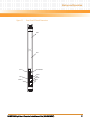
MVME3100 Single Board Computer
Installation and Use
P/N: 6806800M28C
December 2012
©
2011 Emerson
All rights reserved.
Trademarks
Emerson, Business-Critical Continuity, Emerson Network Power and the Emerson Network Power logo are trademarks and service
marks of Emerson Electric Co. © 2008 Emerson Electric Co. All other product or service names are the property of their respective
owners.
Intel® is a trademark or registered trademark of Intel Corporation or its subsidiaries in the United States and other countries.
Java™ and all other Java-based marks are trademarks or registered trademarks of Sun Microsystems, Inc. in the U.S. and other
countries.
Microsoft®, Windows® and Windows Me® are registered trademarks of Microsoft Corporation; and Windows XP™ is a trademark of
Microsoft Corporation.
PICMG®, CompactPCI®, AdvancedTCA™ and the PICMG, CompactPCI and AdvancedTCA logos are registered trademarks of the PCI
Industrial Computer Manufacturers Group.
UNIX® is a registered trademark of The Open Group in the United States and other countries.
Notice
While reasonable efforts have been made to assure the accuracy of this document, Emerson assumes no liability resulting from any
omissions in this document, or from the use of the information obtained therein. Emerson reserves the right to revise this document
and to make changes from time to time in the content hereof without obligation of Emerson to notify any person of such revision or
changes.
Electronic versions of this material may be read online, downloaded for personal use, or referenced in another document as a URL to
a Emerson website. The text itself may not be published commercially in print or electronic form, edited, translated, or otherwise
altered without the permission of Emerson,
It is possible that this publication may contain reference to or information about Emerson products (machines and programs),
programming, or services that are not available in your country. Such references or information must not be construed to mean that
Emerson intends to announce such Emerson products, programming, or services in your country.
Limited and Restricted Rights Legend
If the documentation contained herein is supplied, directly or indirectly, to the U.S. Government, the following notice shall apply
unless otherwise agreed to in writing by Emerson.
Use, duplication, or disclosure by the Government is subject to restrictions as set forth in subparagraph (b)(3) of the Rights in
Technical Data clause at DFARS 252.227-7013 (Nov. 1995) and of the Rights in Noncommercial Computer Software and
Documentation clause at DFARS 252.227-7014 (Jun. 1995).
Contact Address
Emerson Network Power - Embedded Computing
2900 South Diablo Way, Suite 190
Tempe, AZ 85282
USA
Contents
About this Manual . . . . . . . . . . . . . . . . . . . . . . . . . . . . . . . . . . . . . . . . . . . . . . . . . . . . . . . . . . . . . . . . . . . . . . . 13
1
Hardware Preparation and Installation . . . . . . . . . . . . . . . . . . . . . . . . . . . . . . . . . . . . . . . . . . . . . . . . . 19
1.1
1.2
1.3
1.4
1.5
1.6
2
Startup and Operation . . . . . . . . . . . . . . . . . . . . . . . . . . . . . . . . . . . . . . . . . . . . . . . . . . . . . . . . . . . . . . . . 33
2.1
2.2
2.3
3
Overview . . . . . . . . . . . . . . . . . . . . . . . . . . . . . . . . . . . . . . . . . . . . . . . . . . . . . . . . . . . . . . . . . . . . . . . . . . 19
Getting Started . . . . . . . . . . . . . . . . . . . . . . . . . . . . . . . . . . . . . . . . . . . . . . . . . . . . . . . . . . . . . . . . . . . . 19
1.2.1 Overview of Startup Procedures. . . . . . . . . . . . . . . . . . . . . . . . . . . . . . . . . . . . . . . . . . . . . . . . 19
1.2.2 Unpacking Guidelines . . . . . . . . . . . . . . . . . . . . . . . . . . . . . . . . . . . . . . . . . . . . . . . . . . . . . . . . 20
Configuring Hardware . . . . . . . . . . . . . . . . . . . . . . . . . . . . . . . . . . . . . . . . . . . . . . . . . . . . . . . . . . . . . . 20
1.3.1 MVME3100 Layout . . . . . . . . . . . . . . . . . . . . . . . . . . . . . . . . . . . . . . . . . . . . . . . . . . . . . . . . . . . 21
1.3.2 Configuration Switch (S4) . . . . . . . . . . . . . . . . . . . . . . . . . . . . . . . . . . . . . . . . . . . . . . . . . . . . . 24
1.3.3 Geographical Address Switch (S3) . . . . . . . . . . . . . . . . . . . . . . . . . . . . . . . . . . . . . . . . . . . . . . 25
1.3.4 PMC I/O Voltage Configuration . . . . . . . . . . . . . . . . . . . . . . . . . . . . . . . . . . . . . . . . . . . . . . . . 27
1.3.5 RTM SEEPROM Address Switch (S1). . . . . . . . . . . . . . . . . . . . . . . . . . . . . . . . . . . . . . . . . . . . . 27
Installing Hardware . . . . . . . . . . . . . . . . . . . . . . . . . . . . . . . . . . . . . . . . . . . . . . . . . . . . . . . . . . . . . . . . . 28
Connecting to Peripherals . . . . . . . . . . . . . . . . . . . . . . . . . . . . . . . . . . . . . . . . . . . . . . . . . . . . . . . . . . . 29
Completing the Installation . . . . . . . . . . . . . . . . . . . . . . . . . . . . . . . . . . . . . . . . . . . . . . . . . . . . . . . . . . 31
Introduction . . . . . . . . . . . . . . . . . . . . . . . . . . . . . . . . . . . . . . . . . . . . . . . . . . . . . . . . . . . . . . . . . . . . . . . 33
Applying Power . . . . . . . . . . . . . . . . . . . . . . . . . . . . . . . . . . . . . . . . . . . . . . . . . . . . . . . . . . . . . . . . . . . . 33
Switches and Indicators . . . . . . . . . . . . . . . . . . . . . . . . . . . . . . . . . . . . . . . . . . . . . . . . . . . . . . . . . . . . . 33
MOTLoad Firmware . . . . . . . . . . . . . . . . . . . . . . . . . . . . . . . . . . . . . . . . . . . . . . . . . . . . . . . . . . . . . . . . . . 39
3.1
3.2
3.3
3.4
3.5
Overview . . . . . . . . . . . . . . . . . . . . . . . . . . . . . . . . . . . . . . . . . . . . . . . . . . . . . . . . . . . . . . . . . . . . . . . . . . 39
Implementation and Memory Requirements . . . . . . . . . . . . . . . . . . . . . . . . . . . . . . . . . . . . . . . . . . . 39
MOTLoad Commands . . . . . . . . . . . . . . . . . . . . . . . . . . . . . . . . . . . . . . . . . . . . . . . . . . . . . . . . . . . . . . . 39
3.3.1 Utilities . . . . . . . . . . . . . . . . . . . . . . . . . . . . . . . . . . . . . . . . . . . . . . . . . . . . . . . . . . . . . . . . . . . . . 39
3.3.2 Tests . . . . . . . . . . . . . . . . . . . . . . . . . . . . . . . . . . . . . . . . . . . . . . . . . . . . . . . . . . . . . . . . . . . . . . . 40
3.3.3 Command List . . . . . . . . . . . . . . . . . . . . . . . . . . . . . . . . . . . . . . . . . . . . . . . . . . . . . . . . . . . . . . . 41
Using the Command Line Interface . . . . . . . . . . . . . . . . . . . . . . . . . . . . . . . . . . . . . . . . . . . . . . . . . . . 46
3.4.1 Command Line Rules . . . . . . . . . . . . . . . . . . . . . . . . . . . . . . . . . . . . . . . . . . . . . . . . . . . . . . . . . 48
3.4.2 Command Line Help. . . . . . . . . . . . . . . . . . . . . . . . . . . . . . . . . . . . . . . . . . . . . . . . . . . . . . . . . . 48
Firmware Settings . . . . . . . . . . . . . . . . . . . . . . . . . . . . . . . . . . . . . . . . . . . . . . . . . . . . . . . . . . . . . . . . . . 49
3.5.1 Default VME Settings . . . . . . . . . . . . . . . . . . . . . . . . . . . . . . . . . . . . . . . . . . . . . . . . . . . . . . . . . 49
MVME3100 Single Board Computer Installation and Use (6806800M28C)
3
Contents
Contents
3.5.2 Control Register/Control Status Register Settings . . . . . . . . . . . . . . . . . . . . . . . . . . . . . . . . 53
3.5.3 Displaying VME Settings . . . . . . . . . . . . . . . . . . . . . . . . . . . . . . . . . . . . . . . . . . . . . . . . . . . . . . 53
3.5.4 Editing VME Settings . . . . . . . . . . . . . . . . . . . . . . . . . . . . . . . . . . . . . . . . . . . . . . . . . . . . . . . . . 54
3.5.5 Deleting VME Settings . . . . . . . . . . . . . . . . . . . . . . . . . . . . . . . . . . . . . . . . . . . . . . . . . . . . . . . . 55
3.5.6 Restoring Default VME Settings . . . . . . . . . . . . . . . . . . . . . . . . . . . . . . . . . . . . . . . . . . . . . . . . 55
3.6 Remote Start . . . . . . . . . . . . . . . . . . . . . . . . . . . . . . . . . . . . . . . . . . . . . . . . . . . . . . . . . . . . . . . . . . . . . . 56
3.7 Alternate Boot Images and Safe Start . . . . . . . . . . . . . . . . . . . . . . . . . . . . . . . . . . . . . . . . . . . . . . . . . 57
3.8 Firmware Startup Sequence Following Reset . . . . . . . . . . . . . . . . . . . . . . . . . . . . . . . . . . . . . . . . . . . 57
3.9 Firmware Scan for Boot Image . . . . . . . . . . . . . . . . . . . . . . . . . . . . . . . . . . . . . . . . . . . . . . . . . . . . . . . 58
3.10 Boot Images . . . . . . . . . . . . . . . . . . . . . . . . . . . . . . . . . . . . . . . . . . . . . . . . . . . . . . . . . . . . . . . . . . . . . . . 60
3.10.1 Checksum Algorithm . . . . . . . . . . . . . . . . . . . . . . . . . . . . . . . . . . . . . . . . . . . . . . . . . . . . . . . . . 60
3.10.2 Image Flags . . . . . . . . . . . . . . . . . . . . . . . . . . . . . . . . . . . . . . . . . . . . . . . . . . . . . . . . . . . . . . . . . 61
3.10.3 User Images . . . . . . . . . . . . . . . . . . . . . . . . . . . . . . . . . . . . . . . . . . . . . . . . . . . . . . . . . . . . . . . . . 62
3.10.4 Alternate Boot Data Structure . . . . . . . . . . . . . . . . . . . . . . . . . . . . . . . . . . . . . . . . . . . . . . . . . 63
3.10.5 Alternate Boot Images and Safe Start . . . . . . . . . . . . . . . . . . . . . . . . . . . . . . . . . . . . . . . . . . . 63
3.10.6 Boot Image Firmware Scan . . . . . . . . . . . . . . . . . . . . . . . . . . . . . . . . . . . . . . . . . . . . . . . . . . . . 64
3.11 Startup Sequence . . . . . . . . . . . . . . . . . . . . . . . . . . . . . . . . . . . . . . . . . . . . . . . . . . . . . . . . . . . . . . . . . . 65
4
Functional Description . . . . . . . . . . . . . . . . . . . . . . . . . . . . . . . . . . . . . . . . . . . . . . . . . . . . . . . . . . . . . . . . 67
4.1
4.2
4.3
4.4
4.5
4.6
Overview . . . . . . . . . . . . . . . . . . . . . . . . . . . . . . . . . . . . . . . . . . . . . . . . . . . . . . . . . . . . . . . . . . . . . . . . . . 67
Features . . . . . . . . . . . . . . . . . . . . . . . . . . . . . . . . . . . . . . . . . . . . . . . . . . . . . . . . . . . . . . . . . . . . . . . . . . . 67
Block Diagrams . . . . . . . . . . . . . . . . . . . . . . . . . . . . . . . . . . . . . . . . . . . . . . . . . . . . . . . . . . . . . . . . . . . . 71
Processor . . . . . . . . . . . . . . . . . . . . . . . . . . . . . . . . . . . . . . . . . . . . . . . . . . . . . . . . . . . . . . . . . . . . . . . . . . 72
System Memory . . . . . . . . . . . . . . . . . . . . . . . . . . . . . . . . . . . . . . . . . . . . . . . . . . . . . . . . . . . . . . . . . . . . 72
Local Bus Interface . . . . . . . . . . . . . . . . . . . . . . . . . . . . . . . . . . . . . . . . . . . . . . . . . . . . . . . . . . . . . . . . . . 73
4.6.1 Flash Memory . . . . . . . . . . . . . . . . . . . . . . . . . . . . . . . . . . . . . . . . . . . . . . . . . . . . . . . . . . . . . . . 73
4.6.2 Control and Timers Logic. . . . . . . . . . . . . . . . . . . . . . . . . . . . . . . . . . . . . . . . . . . . . . . . . . . . . . 73
4.7 I2C Serial Interface and Devices . . . . . . . . . . . . . . . . . . . . . . . . . . . . . . . . . . . . . . . . . . . . . . . . . . . . . . 74
4.8 Ethernet Interfaces . . . . . . . . . . . . . . . . . . . . . . . . . . . . . . . . . . . . . . . . . . . . . . . . . . . . . . . . . . . . . . . . . 74
4.9 Asynchronous Serial Ports . . . . . . . . . . . . . . . . . . . . . . . . . . . . . . . . . . . . . . . . . . . . . . . . . . . . . . . . . . . 75
4.10 PCI/PCI-X Interfaces and Devices . . . . . . . . . . . . . . . . . . . . . . . . . . . . . . . . . . . . . . . . . . . . . . . . . . . . . 75
4.10.1 MPC8540 PCI-X Interface . . . . . . . . . . . . . . . . . . . . . . . . . . . . . . . . . . . . . . . . . . . . . . . . . . . . . 75
4.10.2 TSi148 VME Controller . . . . . . . . . . . . . . . . . . . . . . . . . . . . . . . . . . . . . . . . . . . . . . . . . . . . . . . . 76
4.10.3 Serial ATA Host Controller. . . . . . . . . . . . . . . . . . . . . . . . . . . . . . . . . . . . . . . . . . . . . . . . . . . . . 76
4.10.4 PCI-X-to-PCI-X Bridges . . . . . . . . . . . . . . . . . . . . . . . . . . . . . . . . . . . . . . . . . . . . . . . . . . . . . . . . 76
4
MVME3100 Single Board Computer Installation and Use (6806800M28C)
Contents
4.11
4.12
4.13
4.14
5
Pin Assignments. . . . . . . . . . . . . . . . . . . . . . . . . . . . . . . . . . . . . . . . . . . . . . . . . . . . . . . . . . . . . . . . . . . . . . 81
5.1
5.2
5.3
6
4.10.5 PCI Mezzanine Card Slots. . . . . . . . . . . . . . . . . . . . . . . . . . . . . . . . . . . . . . . . . . . . . . . . . . . . . . 77
4.10.6 USB . . . . . . . . . . . . . . . . . . . . . . . . . . . . . . . . . . . . . . . . . . . . . . . . . . . . . . . . . . . . . . . . . . . . . . . . 78
4.10.7 PMC Expansion . . . . . . . . . . . . . . . . . . . . . . . . . . . . . . . . . . . . . . . . . . . . . . . . . . . . . . . . . . . . . . 78
General-Purpose Timers . . . . . . . . . . . . . . . . . . . . . . . . . . . . . . . . . . . . . . . . . . . . . . . . . . . . . . . . . . . . . 79
Real-time Clock Battery . . . . . . . . . . . . . . . . . . . . . . . . . . . . . . . . . . . . . . . . . . . . . . . . . . . . . . . . . . . . . 79
Reset Control Logic . . . . . . . . . . . . . . . . . . . . . . . . . . . . . . . . . . . . . . . . . . . . . . . . . . . . . . . . . . . . . . . . . 79
Debug Support . . . . . . . . . . . . . . . . . . . . . . . . . . . . . . . . . . . . . . . . . . . . . . . . . . . . . . . . . . . . . . . . . . . . . 80
Overview . . . . . . . . . . . . . . . . . . . . . . . . . . . . . . . . . . . . . . . . . . . . . . . . . . . . . . . . . . . . . . . . . . . . . . . . . . 81
Connectors . . . . . . . . . . . . . . . . . . . . . . . . . . . . . . . . . . . . . . . . . . . . . . . . . . . . . . . . . . . . . . . . . . . . . . . . 81
5.2.1 PMC Expansion Connector (J4) . . . . . . . . . . . . . . . . . . . . . . . . . . . . . . . . . . . . . . . . . . . . . . . . . 82
5.2.2 Ethernet Connectors (GENET1/J41B, GENET2/J2B, ENET1/J2A) . . . . . . . . . . . . . . . . . . . . . 85
5.2.3 PCI Mezzanine Card (PMC) Connectors (J11 — J14, J21 — J23) . . . . . . . . . . . . . . . . . . . . . . . 85
5.2.4 Serial Port Connectors (COM1/J41A, COM2—COM5/J2A-D) . . . . . . . . . . . . . . . . . . . . . . . . 95
5.2.5 VMEbus P1 Connector . . . . . . . . . . . . . . . . . . . . . . . . . . . . . . . . . . . . . . . . . . . . . . . . . . . . . . . . 95
5.2.6 VMEbus P2 Connector . . . . . . . . . . . . . . . . . . . . . . . . . . . . . . . . . . . . . . . . . . . . . . . . . . . . . . . . 97
5.2.7 MVME721 PMC I/O Module (PIM) Connectors (J10, J14) . . . . . . . . . . . . . . . . . . . . . . . . . . . 98
5.2.8 Planar sATA Power Connector (J30). . . . . . . . . . . . . . . . . . . . . . . . . . . . . . . . . . . . . . . . . . . . 100
5.2.9 USB Connector (J27). . . . . . . . . . . . . . . . . . . . . . . . . . . . . . . . . . . . . . . . . . . . . . . . . . . . . . . . . 100
5.2.10 sATA Connectors (J28 and J29). . . . . . . . . . . . . . . . . . . . . . . . . . . . . . . . . . . . . . . . . . . . . . . . 101
Headers . . . . . . . . . . . . . . . . . . . . . . . . . . . . . . . . . . . . . . . . . . . . . . . . . . . . . . . . . . . . . . . . . . . . . . . . . . 101
5.3.1 Boundary Scan Header (J24) . . . . . . . . . . . . . . . . . . . . . . . . . . . . . . . . . . . . . . . . . . . . . . . . . . 101
5.3.2 Processor COP Header (J25) . . . . . . . . . . . . . . . . . . . . . . . . . . . . . . . . . . . . . . . . . . . . . . . . . . 102
Memory Maps . . . . . . . . . . . . . . . . . . . . . . . . . . . . . . . . . . . . . . . . . . . . . . . . . . . . . . . . . . . . . . . . . . . . . . 103
6.1
Memory Maps . . . . . . . . . . . . . . . . . . . . . . . . . . . . . . . . . . . . . . . . . . . . . . . . . . . . . . . . . . . . . . . . . . . . . 103
6.1.1 Default Processor Memory Map . . . . . . . . . . . . . . . . . . . . . . . . . . . . . . . . . . . . . . . . . . . . . . . 103
6.1.2 MOTLoad’s Processor Memory Map . . . . . . . . . . . . . . . . . . . . . . . . . . . . . . . . . . . . . . . . . . . 104
6.1.3 VME Memory Map. . . . . . . . . . . . . . . . . . . . . . . . . . . . . . . . . . . . . . . . . . . . . . . . . . . . . . . . . . . 104
6.1.4 System I/O Memory Map . . . . . . . . . . . . . . . . . . . . . . . . . . . . . . . . . . . . . . . . . . . . . . . . . . . . . 105
6.1.5 System Status Register . . . . . . . . . . . . . . . . . . . . . . . . . . . . . . . . . . . . . . . . . . . . . . . . . . . . . . 107
6.1.6 System Control Register . . . . . . . . . . . . . . . . . . . . . . . . . . . . . . . . . . . . . . . . . . . . . . . . . . . . . 108
6.1.7 System Indicator Register . . . . . . . . . . . . . . . . . . . . . . . . . . . . . . . . . . . . . . . . . . . . . . . . . . . . 109
MVME3100 Single Board Computer Installation and Use (6806800M28C)
5
Contents
Contents
6.1.8
6.1.9
6.1.10
6.1.11
6.1.12
6.1.13
6.1.14
6.1.15
6.1.16
Flash Control/Status Register . . . . . . . . . . . . . . . . . . . . . . . . . . . . . . . . . . . . . . . . . . . . . . . . . 110
PCI Bus Status Registers. . . . . . . . . . . . . . . . . . . . . . . . . . . . . . . . . . . . . . . . . . . . . . . . . . . . . . 111
Interrupt Detect Register . . . . . . . . . . . . . . . . . . . . . . . . . . . . . . . . . . . . . . . . . . . . . . . . . . . . 114
Presence Detect Register . . . . . . . . . . . . . . . . . . . . . . . . . . . . . . . . . . . . . . . . . . . . . . . . . . . . 114
PLD Revision Register . . . . . . . . . . . . . . . . . . . . . . . . . . . . . . . . . . . . . . . . . . . . . . . . . . . . . . . . 115
PLD Data Code Register . . . . . . . . . . . . . . . . . . . . . . . . . . . . . . . . . . . . . . . . . . . . . . . . . . . . . . 116
Test Register 1 . . . . . . . . . . . . . . . . . . . . . . . . . . . . . . . . . . . . . . . . . . . . . . . . . . . . . . . . . . . . . . 116
Test Register 2 . . . . . . . . . . . . . . . . . . . . . . . . . . . . . . . . . . . . . . . . . . . . . . . . . . . . . . . . . . . . . . 117
External Timer Registers . . . . . . . . . . . . . . . . . . . . . . . . . . . . . . . . . . . . . . . . . . . . . . . . . . . . . 117
6.1.16.1 Prescalar Register . . . . . . . . . . . . . . . . . . . . . . . . . . . . . . . . . . . . . . . . . . . . . . . . . . 117
6.1.16.2 Control Registers . . . . . . . . . . . . . . . . . . . . . . . . . . . . . . . . . . . . . . . . . . . . . . . . . . 118
6.1.16.3 Compare Registers . . . . . . . . . . . . . . . . . . . . . . . . . . . . . . . . . . . . . . . . . . . . . . . . . 119
6.1.16.4 Counter Registers . . . . . . . . . . . . . . . . . . . . . . . . . . . . . . . . . . . . . . . . . . . . . . . . . . 120
6.1.17 Geographical Address Register . . . . . . . . . . . . . . . . . . . . . . . . . . . . . . . . . . . . . . . . . . . . . . . 120
7
Programming Details . . . . . . . . . . . . . . . . . . . . . . . . . . . . . . . . . . . . . . . . . . . . . . . . . . . . . . . . . . . . . . . . 121
7.1
7.2
7.3
7.4
7.5
7.6
7.7
7.8
7.9
7.10
7.11
7.12
7.13
7.14
7.15
A
Specifications . . . . . . . . . . . . . . . . . . . . . . . . . . . . . . . . . . . . . . . . . . . . . . . . . . . . . . . . . . . . . . . . . . . . . . . 137
A.1
6
Introduction . . . . . . . . . . . . . . . . . . . . . . . . . . . . . . . . . . . . . . . . . . . . . . . . . . . . . . . . . . . . . . . . . . . . . . 121
MPC8540 Reset Configuration . . . . . . . . . . . . . . . . . . . . . . . . . . . . . . . . . . . . . . . . . . . . . . . . . . . . . . 122
MPC8540 Interrupt Controller . . . . . . . . . . . . . . . . . . . . . . . . . . . . . . . . . . . . . . . . . . . . . . . . . . . . . . 127
Local Bus Controller Chip Select Assignments . . . . . . . . . . . . . . . . . . . . . . . . . . . . . . . . . . . . . . . . . 128
Two-Wire Serial Interface . . . . . . . . . . . . . . . . . . . . . . . . . . . . . . . . . . . . . . . . . . . . . . . . . . . . . . . . . . . 128
User Configuration EEPROM . . . . . . . . . . . . . . . . . . . . . . . . . . . . . . . . . . . . . . . . . . . . . . . . . . . . . . . . 129
VPD EEPROM . . . . . . . . . . . . . . . . . . . . . . . . . . . . . . . . . . . . . . . . . . . . . . . . . . . . . . . . . . . . . . . . . . . . . 130
RTM VPD EEPROM . . . . . . . . . . . . . . . . . . . . . . . . . . . . . . . . . . . . . . . . . . . . . . . . . . . . . . . . . . . . . . . . . 130
Ethernet PHY Address . . . . . . . . . . . . . . . . . . . . . . . . . . . . . . . . . . . . . . . . . . . . . . . . . . . . . . . . . . . . . . 130
Flash Memory . . . . . . . . . . . . . . . . . . . . . . . . . . . . . . . . . . . . . . . . . . . . . . . . . . . . . . . . . . . . . . . . . . . . . 131
PCI IDSEL Definition . . . . . . . . . . . . . . . . . . . . . . . . . . . . . . . . . . . . . . . . . . . . . . . . . . . . . . . . . . . . . . . . 132
PCI Arbitration Assignments . . . . . . . . . . . . . . . . . . . . . . . . . . . . . . . . . . . . . . . . . . . . . . . . . . . . . . . . 134
Clock Distribution . . . . . . . . . . . . . . . . . . . . . . . . . . . . . . . . . . . . . . . . . . . . . . . . . . . . . . . . . . . . . . . . . 134
MPC8540 Real-Time Clock Input . . . . . . . . . . . . . . . . . . . . . . . . . . . . . . . . . . . . . . . . . . . . . . . . . . . . 136
MPC8540 LBC Clock Divisor . . . . . . . . . . . . . . . . . . . . . . . . . . . . . . . . . . . . . . . . . . . . . . . . . . . . . . . . . 136
Power Requirements . . . . . . . . . . . . . . . . . . . . . . . . . . . . . . . . . . . . . . . . . . . . . . . . . . . . . . . . . . . . . . . 137
MVME3100 Single Board Computer Installation and Use (6806800M28C)
Contents
A.2
A.3
B
Environmental Specifications . . . . . . . . . . . . . . . . . . . . . . . . . . . . . . . . . . . . . . . . . . . . . . . . . . . . . . . 137
Thermally Significant Components . . . . . . . . . . . . . . . . . . . . . . . . . . . . . . . . . . . . . . . . . . . . . . . . . . 138
Related Documentation . . . . . . . . . . . . . . . . . . . . . . . . . . . . . . . . . . . . . . . . . . . . . . . . . . . . . . . . . . . . . . 141
B.1
B.2
B.3
Emerson Network Power - Embedded Computing Documents . . . . . . . . . . . . . . . . . . . . . . . . . . 141
Manufacturers’ Documents . . . . . . . . . . . . . . . . . . . . . . . . . . . . . . . . . . . . . . . . . . . . . . . . . . . . . . . . . 141
Related Specifications . . . . . . . . . . . . . . . . . . . . . . . . . . . . . . . . . . . . . . . . . . . . . . . . . . . . . . . . . . . . . . 143
Safety Notes . . . . . . . . . . . . . . . . . . . . . . . . . . . . . . . . . . . . . . . . . . . . . . . . . . . . . . . . . . . . . . . . . . . . . . . . . . . . 146
Sicherheitshinweise . . . . . . . . . . . . . . . . . . . . . . . . . . . . . . . . . . . . . . . . . . . . . . . . . . . . . . . . . . . . . . . . . . . . . 150
MVME3100 Single Board Computer Installation and Use (6806800M28C)
7
Contents
Contents
8
MVME3100 Single Board Computer Installation and Use (6806800M28C)
List of Tables
Table 1-1
Table 1-2
Table 1-3
Table 1-4
Table 1-5
Table 1-6
Table 1-7
Table 1-8
Table 2-1
Table 2-2
Table 2-3
Table 3-1
Table 3-2
Table 4-1
Table 4-2
Table 5-1
Table 5-2
Table 5-3
Table 5-4
Table 5-5
Table 5-6
Table 5-7
Table 5-8
Table 5-9
Table 5-10
Table 5-11
Table 5-12
Table 5-13
Table 5-14
Table 5-15
Table 5-16
Table 5-17
Table 5-18
Table 6-1
Table 6-2
Table 6-3
Startup Overview . . . . . . . . . . . . . . . . . . . . . . . . . . . . . . . . . . . . . . . . . . . . . . . . . . . . . . . . . . . 19
Configuration Switch (S4) Settings . . . . . . . . . . . . . . . . . . . . . . . . . . . . . . . . . . . . . . . . . . . . 24
Geographical Address Switch Assignments . . . . . . . . . . . . . . . . . . . . . . . . . . . . . . . . . . . . . 25
Slot Geographical Address Settings . . . . . . . . . . . . . . . . . . . . . . . . . . . . . . . . . . . . . . . . . . . . 26
RTM EEPROM Address Switch Assignments . . . . . . . . . . . . . . . . . . . . . . . . . . . . . . . . . . . . . 27
EEPROM Address Settings . . . . . . . . . . . . . . . . . . . . . . . . . . . . . . . . . . . . . . . . . . . . . . . . . . . . 27
MVME3100 Connectors . . . . . . . . . . . . . . . . . . . . . . . . . . . . . . . . . . . . . . . . . . . . . . . . . . . . . . 30
MVME721 Rear Transition Module Connectors . . . . . . . . . . . . . . . . . . . . . . . . . . . . . . . . . . 30
Front-Panel LED Status Indicators . . . . . . . . . . . . . . . . . . . . . . . . . . . . . . . . . . . . . . . . . . . . . 33
MVME721 LED Status Indicators . . . . . . . . . . . . . . . . . . . . . . . . . . . . . . . . . . . . . . . . . . . . . . 36
Additional Onboard Status Indicators . . . . . . . . . . . . . . . . . . . . . . . . . . . . . . . . . . . . . . . . . . 36
MOTLoad Commands . . . . . . . . . . . . . . . . . . . . . . . . . . . . . . . . . . . . . . . . . . . . . . . . . . . . . . . 41
MOTLoad Image Flags . . . . . . . . . . . . . . . . . . . . . . . . . . . . . . . . . . . . . . . . . . . . . . . . . . . . . . . 61
MVME3100 Features Summary . . . . . . . . . . . . . . . . . . . . . . . . . . . . . . . . . . . . . . . . . . . . . . . 67
MVME721 RTM Features Summary . . . . . . . . . . . . . . . . . . . . . . . . . . . . . . . . . . . . . . . . . . . . 69
PMC Expansion Connector (J4) Pin Assignments . . . . . . . . . . . . . . . . . . . . . . . . . . . . . . . . 82
Ethernet Connectors Pin Assignment . . . . . . . . . . . . . . . . . . . . . . . . . . . . . . . . . . . . . . . . . . 85
PMC Slot 1 Connector (J11) Pin Assignments . . . . . . . . . . . . . . . . . . . . . . . . . . . . . . . . . . . 85
PMC Slot 1 Connector (J12) Pin Assignments . . . . . . . . . . . . . . . . . . . . . . . . . . . . . . . . . . . 87
PMC Slot 1 Connector (J13) Pin Assignments . . . . . . . . . . . . . . . . . . . . . . . . . . . . . . . . . . . 88
PMC Slot 1 Connector (J14) Pin Assignments . . . . . . . . . . . . . . . . . . . . . . . . . . . . . . . . . . . 89
PMC Slot 2 Connector (J21) Pin Assignments . . . . . . . . . . . . . . . . . . . . . . . . . . . . . . . . . . . 91
PMC Slot 2 Connector (J22) Pin Assignments . . . . . . . . . . . . . . . . . . . . . . . . . . . . . . . . . . . 92
PMC Slot 2 Connector (J23) Pin Assignments . . . . . . . . . . . . . . . . . . . . . . . . . . . . . . . . . . . 93
COM Port Connector Pin Assignments . . . . . . . . . . . . . . . . . . . . . . . . . . . . . . . . . . . . . . . . . 95
VMEbus P1 Connector Pin Assignments . . . . . . . . . . . . . . . . . . . . . . . . . . . . . . . . . . . . . . . . 95
VME P2 Connector Pinouts . . . . . . . . . . . . . . . . . . . . . . . . . . . . . . . . . . . . . . . . . . . . . . . . . . . 97
MVME721 Host I/O Connector (J10) Pin Assignments . . . . . . . . . . . . . . . . . . . . . . . . . . . . 98
Planar sATA Power Connector (J30) Pin Assignments . . . . . . . . . . . . . . . . . . . . . . . . . . . . 100
USB Connector (J27) Pin Assignments . . . . . . . . . . . . . . . . . . . . . . . . . . . . . . . . . . . . . . . . 100
sATA Connectors (J28 and J29) Pin Assignments . . . . . . . . . . . . . . . . . . . . . . . . . . . . . . . . 101
Boundary Scan Header (J24) Pin Assignments . . . . . . . . . . . . . . . . . . . . . . . . . . . . . . . . . . 101
Processor COP Header (J25) Pin Assignments . . . . . . . . . . . . . . . . . . . . . . . . . . . . . . . . . . 102
Default Processor Address Map . . . . . . . . . . . . . . . . . . . . . . . . . . . . . . . . . . . . . . . . . . . . . . 103
MOTLoad’s Processor Address Map . . . . . . . . . . . . . . . . . . . . . . . . . . . . . . . . . . . . . . . . . . . 104
System I/O Memory Map . . . . . . . . . . . . . . . . . . . . . . . . . . . . . . . . . . . . . . . . . . . . . . . . . . . . 105
MVME3100 Single Board Computer Installation and Use (6806800M28C)
9
List of Tables
Table 6-4
Table 6-5
Table 6-6
Table 6-7
Table 6-8
Table 6-9
Table 6-10
Table 6-11
Table 6-12
Table 6-13
Table 6-14
Table 6-15
Table 6-16
Table 6-17
Table 6-18
Table 6-19
Table 6-20
Table 7-1
Table 7-2
Table 7-3
Table 7-4
Table 7-5
Table 7-6
Table 7-7
Table 7-8
Table 7-9
Table 7-10
Table A-1
Table A-2
Table A-3
Table B-1
Table B-2
Table B-3
10
System Status Register . . . . . . . . . . . . . . . . . . . . . . . . . . . . . . . . . . . . . . . . . . . . . . . . . . . . . . 107
System Control Register . . . . . . . . . . . . . . . . . . . . . . . . . . . . . . . . . . . . . . . . . . . . . . . . . . . . . 108
System Indicator Register . . . . . . . . . . . . . . . . . . . . . . . . . . . . . . . . . . . . . . . . . . . . . . . . . . . 109
Flash Control/Status Register . . . . . . . . . . . . . . . . . . . . . . . . . . . . . . . . . . . . . . . . . . . . . . . . 110
PCI Bus A Status Register . . . . . . . . . . . . . . . . . . . . . . . . . . . . . . . . . . . . . . . . . . . . . . . . . . . .111
PCI Bus B Status Register . . . . . . . . . . . . . . . . . . . . . . . . . . . . . . . . . . . . . . . . . . . . . . . . . . . .111
PCI Bus C Status Register . . . . . . . . . . . . . . . . . . . . . . . . . . . . . . . . . . . . . . . . . . . . . . . . . . . .113
Interrupt Detect Register . . . . . . . . . . . . . . . . . . . . . . . . . . . . . . . . . . . . . . . . . . . . . . . . . . . . 114
Presence Detect Register . . . . . . . . . . . . . . . . . . . . . . . . . . . . . . . . . . . . . . . . . . . . . . . . . . . . 114
PLD Revision Register . . . . . . . . . . . . . . . . . . . . . . . . . . . . . . . . . . . . . . . . . . . . . . . . . . . . . . . 115
PLD Data Code Register . . . . . . . . . . . . . . . . . . . . . . . . . . . . . . . . . . . . . . . . . . . . . . . . . . . . . 116
Test Register 1 . . . . . . . . . . . . . . . . . . . . . . . . . . . . . . . . . . . . . . . . . . . . . . . . . . . . . . . . . . . . . 116
Test Register 2 . . . . . . . . . . . . . . . . . . . . . . . . . . . . . . . . . . . . . . . . . . . . . . . . . . . . . . . . . . . . . 117
Prescalar Register . . . . . . . . . . . . . . . . . . . . . . . . . . . . . . . . . . . . . . . . . . . . . . . . . . . . . . . . . . 117
Tick Timer Control Registers . . . . . . . . . . . . . . . . . . . . . . . . . . . . . . . . . . . . . . . . . . . . . . . . . 118
Tick Timer Compare Registers . . . . . . . . . . . . . . . . . . . . . . . . . . . . . . . . . . . . . . . . . . . . . . . 119
Tick Timer Counter Registers . . . . . . . . . . . . . . . . . . . . . . . . . . . . . . . . . . . . . . . . . . . . . . . . 120
MPC8540 Power-on Reset Configuration Settings . . . . . . . . . . . . . . . . . . . . . . . . . . . . . . 122
MPC8540 Interrupt Controller . . . . . . . . . . . . . . . . . . . . . . . . . . . . . . . . . . . . . . . . . . . . . . . 127
LBC Chip Select Assignments . . . . . . . . . . . . . . . . . . . . . . . . . . . . . . . . . . . . . . . . . . . . . . . . 128
I2C Bus Device Addressing . . . . . . . . . . . . . . . . . . . . . . . . . . . . . . . . . . . . . . . . . . . . . . . . . . . 128
PHY Types and MII Management Bus Addresses . . . . . . . . . . . . . . . . . . . . . . . . . . . . . . . . 130
Flash Options . . . . . . . . . . . . . . . . . . . . . . . . . . . . . . . . . . . . . . . . . . . . . . . . . . . . . . . . . . . . . . 131
IDSEL and Interrupt Mapping for PCI Devices . . . . . . . . . . . . . . . . . . . . . . . . . . . . . . . . . . . 132
Planar PCI Device Identification . . . . . . . . . . . . . . . . . . . . . . . . . . . . . . . . . . . . . . . . . . . . . . 133
PCI Arbitration Assignments . . . . . . . . . . . . . . . . . . . . . . . . . . . . . . . . . . . . . . . . . . . . . . . . . 134
Clock Assignments . . . . . . . . . . . . . . . . . . . . . . . . . . . . . . . . . . . . . . . . . . . . . . . . . . . . . . . . . 135
Current Requirements . . . . . . . . . . . . . . . . . . . . . . . . . . . . . . . . . . . . . . . . . . . . . . . . . . . . . . 137
MVME3100 Specifications . . . . . . . . . . . . . . . . . . . . . . . . . . . . . . . . . . . . . . . . . . . . . . . . . . . 137
Thermally Significant Components . . . . . . . . . . . . . . . . . . . . . . . . . . . . . . . . . . . . . . . . . . . 138
Emerson Network Power - Embedded Computing Documents . . . . . . . . . . . . . . . . . . .141
Manufacturers’ Documents . . . . . . . . . . . . . . . . . . . . . . . . . . . . . . . . . . . . . . . . . . . . . . . . . 141
Related Specifications . . . . . . . . . . . . . . . . . . . . . . . . . . . . . . . . . . . . . . . . . . . . . . . . . . . . . . 143
MVME3100 Single Board Computer Installation and Use (6806800M28C)
List of Figures
Figure 1-1
Figure 1-2
Figure 2-1
Figure 4-1
Figure 4-2
Figure A-1
Figure A-2
Board Layout . . . . . . . . . . . . . . . . . . . . . . . . . . . . . . . . . . . . . . . . . . . . . . . . . . . . . . . . . . . 23
Geographical Address Switch Settings . . . . . . . . . . . . . . . . . . . . . . . . . . . . . . . . . . . . . 25
Front Panel LEDs and Connectors . . . . . . . . . . . . . . . . . . . . . . . . . . . . . . . . . . . . . . . . . 35
MVME3100 Block Diagram . . . . . . . . . . . . . . . . . . . . . . . . . . . . . . . . . . . . . . . . . . . . . . . 71
MVME721 RTM Block Diagram . . . . . . . . . . . . . . . . . . . . . . . . . . . . . . . . . . . . . . . . . . . . 72
Primary Side Components . . . . . . . . . . . . . . . . . . . . . . . . . . . . . . . . . . . . . . . . . . . . . . . 139
Secondary Side Components . . . . . . . . . . . . . . . . . . . . . . . . . . . . . . . . . . . . . . . . . . . . 140
MVME3100 Single Board Computer Installation and Use (6806800M28C)
11
List of Figures
12
MVME3100 Single Board Computer Installation and Use (6806800M28C)
About this Manual
Overview of Contents
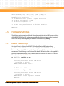
This manual is divided into the following chapters and appendices:
Hardware Preparation and Installation, provides MVME3100 board preparation and installation
instructions, as well as ESD precautionary notes.
Startup and Operation, provides the power-up procedure and identifies the switches and
indicators on the MVMEM3100.
MOTLoad Firmware, describes the basic features of the MOTLoad firmware product.
Functional Description, describes the MVME3100 and the MVME721 RTM on a block diagram
level.
Pin Assignments, provides pin assignments for various headers and connectors on the
MMVE3100 single-board computer.
Memory Maps, provides information on memory maps and system and configuration registers.
Programming Details, provides additional programming information including IDSEL mapping,
interrupt assignments for the MPC8540 interrupt controller, Flash memory, two-wire serial
interface addressing, and other device and system considerations.
Specifications, provides power requirements and environmental specifications.
Related Documentation, provides a listing of related Emerson manuals, vendor documentation,
and industry specifications.
Safety Notes summarizes the safety instructions in the manual.
Sicherheitshinweise is a German translation of the Safety Notes chapter.
The MVME3100 Single-Board Computer Installation and Use manual provides the information you
will need to install and configure your MVME3100 single-board computer and MVME721 rear
transition module (RTM). It provides specific preparation and installation information, and data
applicable to the board.
MVME3100 Single Board Computer Installation and Use (6806800M28C)
13
About this Manual
About this Manual
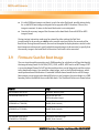
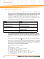
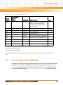
As of the printing date of this manual, the MVME3100 supports the models listed below.
Model Number
Description
MVME3100-1152
677 MHz MPC8540 PowerQUICC III™ integrated processor, 256 MB DDR
SDRAM, 64MB flash, Gigabit Ethernet, SATA, IEEE handles
MVME3100-1263
833 MHz MPC8540 PowerQUICC III integrated processor, 512MB DDR
SDRAM, 128 MB flash, Gigabit Ethernet, SATA, USB, PCI expansion
connector, IEEE handles
MVME721-101
Rear Transition Module, direct connect, 75 mm, PIM socket for PMC-1 I/O,
four serial, 10/100/1000 Enet, 10/100 Enet
Abbreviations
This document uses the following abbreviations:
Abbreviation
Description
AC
Alternating Current
ASIC
Application Specific Integrated Circuit
ATA
Advanced Technology Attachment
BLT
Block Transfer
CMC
Common Mezzanine Card
COM
Communication
COP
Common On-chip Processor
COTS
Commercial-Off-the-Shelf
CPU
Central Processing Unit
CTS
Clear To Send
DC
Direct Current
DDR
Double Data Rate
DIN
Deutsches Insitut für Normung eV
DMA
Direct Memory Access
DPA
Downlink Packet Access
DRAM
Dynamic Random Access Memory
14
MVME3100 Single Board Computer Installation and Use (6806800M28C)
About this Manual
Abbreviation
Description
DUART
Dual Universal Asynchronous Receiver/Transmitter
ECC
Error Correction Code
ENET
Ethernet
ENV
Environment
ESD
Electrostatic Discharge
FAT
File Allocation Table
FEC
Fast Ethernet Controller
FIFO
First In First Out
FPU
Floating Point Unit
GA
Geographic Address
GENET
Gigabit Ethernet
GEV
Global Environment Variable
GMII
Gigabit Media Independent Interface
GPCM
General Purpose Chip select Machine
IBCA
Inter-Board Communication Address
IDE
Integrated Drive Electronics
I/O
Input/Output
IEEE
Institute of Electrical and Electronics Engineers
LBC
Local Bus Controller
LED
Light Emitting Diode
MB
Megabyte
MBLT
Multiplexed Block Transfer
MHz
Megahertz
MIIM
MII Management
MMU
Memory Management Unit
MPU
Memory Protection Unit
Microprocessor Unit
MTBF
Mean Time Between Failure
MVME3100 Single Board Computer Installation and Use (6806800M28C)
15
About this Manual
About this Manual
Abbreviation
Description
NVRAM
Non Volatile RAM
OS
Operating System
PAL
Physical Abstraction Layer
PCB
Printed Circuit Board
PCI
Peripheral Connect Interface
PCI-X
Peripheral Component Interconnect -X
PHY
Physical Layer
PIC
Programmable Interrupt Controller
PIM
PCI Mezzanine Card Input/Output Module
PLD
Programmable Logic Device
PMC
PCI Mezzanine Card (IEEE P1386.1)
POST
Power On S Test
PrPMC
Processor PMC
QUART
Quad Universal Asynchronous Receiver/Transmitter
RAM
Random Access Memory
RTC
Real Time Clock
RTM
Rear Transition Module
RTOS
Real Time Operating System
SATA
Serial AT Attachment
SBC
Single Board Computer
SDRAM
Synchronous Dynamic Random Access Memory
SIG
Special Interest Group
SMT
Surface Mount Technology
SNR
receive data Poor SNR
SPD
Serial Presence Detect
SROM
TFTP
Trivial File Transfer Protocol
TSEC
Triple Speed Ethernet Controllers
16
MVME3100 Single Board Computer Installation and Use (6806800M28C)
About this Manual
Abbreviation
Description
TSOP
Thin Small Outline Package
UART
Universal Asynchronous Receiver/Transmitter
UNIX
UNIX operating system
USB
Universal Serial Bus
VIO
Input/Output Voltage
VITA
VMEbus International Trade Association
VME
VersaModule Eurocard
VMEbus
VersaModule Eurocard bus
VPD
Vital Product Data
WP
Write Protect
Conventions
The following table describes the conventions used throughout this manual.
Notation
Description
0x00000000
Typical notation for hexadecimal numbers (digits are
0 through F), for example used for addresses and
offsets
0b0000
Same for binary numbers (digits are 0 and 1)
bold
Used to emphasize a word
Screen
Used for on-screen output and code related elements
or commands in body text
Courier + Bold
Used to characterize user input and to separate it
from system output
Reference
Used for references and for table and figure
descriptions
File > Exit
Notation for selecting a submenu
<text>
Notation for variables and keys
[text]
Notation for software buttons to click on the screen
and parameter description
MVME3100 Single Board Computer Installation and Use (6806800M28C)
17
About this Manual
About this Manual
Notation
Description
...
Repeated item for example node 1, node 2, ..., node
12
.
Omission of information from example/command
that is not necessary at the time being
.
.
..
Ranges, for example: 0..4 means one of the integers
0,1,2,3, and 4 (used in registers)
|
Logical OR
Indicates a hazardous situation which, if not avoided,
could result in death or serious injury
Indicates a hazardous situation which, if not avoided,
may result in minor or moderate injury
Indicates a property damage message
No danger encountered. Pay attention to important
information
18
MVME3100 Single Board Computer Installation and Use (6806800M28C)
About this Manual
Summary of Changes
This manual has been revised and replaces all prior editions.
Part Number
Publication Date
Description
6806800M28C
December 2012
Added Declaration of Conformity on page 22.
6806800M28B
August 2011
Updated Safety Notes on page 148 and
Sicherheitshinweise on page 152.
6806800M28A
April 2011
EA version
MVME3100 Single Board Computer Installation and Use (6806800M28C)
19
About this Manual
About this Manual
20
MVME3100 Single Board Computer Installation and Use (6806800M28C)
Chapter 1
Hardware Preparation and Installation
1.1
Overview
The MVME3100 is a single-slot, single-board computer based on the MPC8540 PowerQUICC
III™ integrated processor. The MVME3100 provides serial ATA (sATA), USB 2.0, 2eSST VMEbus
interfaces, dual 64-bit/100 MHz PMC sites, up to 128MB of Flash, dual 10/100/1000 Ethernet,
one 10/100 Ethernet, and five serial ports. This board supports front and rear I/O and a single
SODIMM module for DDR memory. Access to rear I/O is available with the MVME721 rear
transition module (RTM).
Front-panel connectors on the MVME3100 board include: one RJ-45 connector for the Gigabit
Ethernet, one RJ-45 connector for the asynchronous serial port, one USB port with one type A
connector, one sATA port with one external sATA connector, and a combined reset and abort
switch.
Rear-panel connectors on the MVME721 board include: one RJ-45 connector for each of the
10/100 and 10/100/1000 BaseT Ethernets and four RJ-45 connectors for the asynchronous
serial ports. The RTM also provides two planar connectors for one PIM with rear I/O.
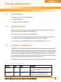
1.2
Getting Started
This section provides an overview of the steps necessary to install and power up the
MVME3100 and a brief section on unpacking and ESD precautions.
1.2.1
Overview of Startup Procedures
The following table lists the things you will need to do before you can use this board and tells
where to find the information you need to perform each step. Be sure to read this entire
chapter, including all Caution and Warning notes, before you begin.
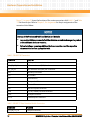
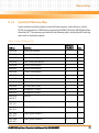
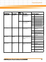
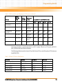
Table 1-1 Startup Overview
What you need to do...
Refer to...
Unpack the hardware.
Unpacking Guidelines on page 22
Identify various components on the board.
MVME3100 Layout on page 23
Install the MVME3100 board in a chassis.
on page 30
MVME3100 Single Board Computer Installation and Use (6806800M28C)
21
Hardware Preparation and Installation
Table 1-1 Startup Overview (continued)
What you need to do...
Refer to...
Connect any other equipment you will be using
Connecting to Peripherals on page 31
Verify the hardware is installed.
Completing the Installation on page 33
1.2.2
Unpacking Guidelines
Unpack the equipment from the shipping carton. Refer to the packing list and verify that all
items are present. Save the packing material for storing and reshipping of equipment.
If the shipping carton is damaged upon receipt, request that the carrier’s agent be present
during the unpacking and inspection of the equipment.
Damage of Circuits
1.3
z
Electrostatic discharge and incorrect installation and removal of the product can
damage circuits or shorten their life.
z
Before touching the product make sure that your are working in an ESD-safe
environment or wear an ESD wrist strap or ESD shoes. Hold the product by its edges and
do not touch any components or circuits.
Declaration of Conformity
For Declaration of Conformity, refer MVME3100 Series Declaration of Conformity.
1.4
Configuring Hardware
This section discusses certain hardware and software tasks that may need to be performed
prior to installing the board in a chassis.
To produce the desired configuration and ensure proper operation of the MVME3100, you may
need to carry out certain hardware modifications before installing the module.
22
MVME3100 Single Board Computer Installation and Use (6806800M28C)
Hardware Preparation and Installation
Most options on the MVME3100 are software configurable. Configuration changes are made
by setting bits in control registers after the board is installed in a system.
Jumpers/switches are used to control those options that are not software configurable. These
jumper settings are described further on in this section. If you are resetting the board jumpers
from their default settings, it is important to verify that all settings are reset properly.
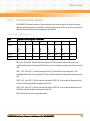
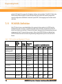
1.4.1
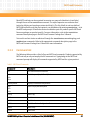
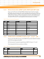
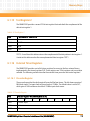
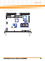
MVME3100 Layout
Figure 1-1 on page 25 illustrates the placement of the jumpers, headers, connectors, switches,
and various other components on the MVME3100.
There are two switch blocks which have user-selectable settings. Refer to Table 1-2, Table 1-3,
and Table 1-4 for switch settings. There is one switch on the MVME721. Refer to Table 1-5 and
Table 1-6 for switch settings.
MVME3100 Single Board Computer Installation and Use (6806800M28C)
23
Hardware Preparation and Installation
The MVME3100 is factory tested and shipped with the configuration described in the following
sections.
24
MVME3100 Single Board Computer Installation and Use (6806800M28C)
Hardware Preparation and Installation
Figure 1-1
Board Layout
J25
J24
J28
U1014
U1049
S4
1
U1050
J30
J21
J22
U1020
U1019
U1052
S3
U1026
1
U1046
U1047
U1027
U5000
U1051
P1
J23
U1025
J11
J12
J13
J14
U21
U1003
U1007
U1010
J2
U1012
U1024
U1012
P2
U1000
J4
MVME3100 Single Board Computer Installation and Use (6806800M28C)
25
Hardware Preparation and Installation
1.4.2
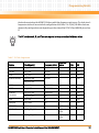
Configuration Switch (S4)
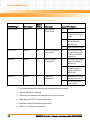
An 8-position SMT configuration switch controls the VME SCON setting, Flash bank writeprotect, and the safe start ENV settings. It also selects the Flash boot image. The default setting
on all switch positions is OFF.
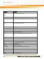
Table 1-2 Configuration Switch (S4) Settings
Setting
Switch
Pos.
OFF (Factory Default)
ON
Notes
SAFE_START
1
Normal ENV settings
should be used.
Safe ENV settings
should be used.
This switch status is
readable from System
Status register 1, bit 5.
Software may check
this bit and act
accordingly.
BOOT BLOCK
SELECT
2
Flash memory map is
normal and boot block A
is selected.
Boot block B is
selected and mapped
to the highest
address.
FLASH BANK WP
3
Entire Flash is not writeprotected.
Flash is writeprotected.
Reserved
4
VME SCON
AUTO/MANUAL
MODE
5
Auto-SCON mode.
Manual SCON mode.
Manual SCON mode
works in conjunction
with the VME SCON
SELECT switch.
MANUAL VME
SCON SELECT
6
Non-SCON mode.
Always SCON mode.
This switch is only
effective when the
VME SCON
AUTO/MANUAL
MODE switch is ON.
Reserved
7
26
MVME3100 Single Board Computer Installation and Use (6806800M28C)
Hardware Preparation and Installation
Table 1-2 Configuration Switch (S4) Settings (continued)
Setting
Switch
Pos.
OFF (Factory Default)
ON
Notes
TRST SELECT
8
Normal MPC8540 TRST
mode where the board
HRESET will assert TRST.
Isolates the board
HRESET from TRST
and allows the board
to reset without
resetting the
MPC8540 JTAG/COP
interface.
This switch should
remain in the OFF
position unless a
MPC8540 emulator is
attached.
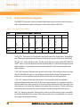
1.4.3
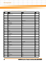
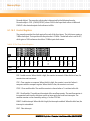
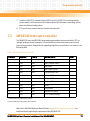
Geographical Address Switch (S3)
The TSi148 VMEbus Status register provides the VMEbus geographical address of the
MVME3100. This switch reflects the inverted states of the geographical address signals.
Applications not using the 5-row backplane can use the geographical address switch to assign
a geographical address.
Figure 1-2
Geographical Address Switch Settings
1
1
16
1
ON
16
ON
Not used
1
2
PCI-X mode
2
PCI-X mode
3
GAP#=0
3
GAP#=1
4
GA4#=0
4
GA4#=1
5
GA3#=0
5
GA3#=1
6
GA2#=0
6
GA2#=1
7
GA1#=0
7
GA1#=1
8
GA0#=0
8
GA0#=1
Not used
Factory Default
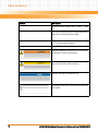
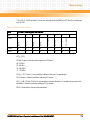
Table 1-3 Geographical Address Switch Assignments
Position
SW1
SW21
SW3
SW4
SW5
SW6
SW7
SW8
Function
Not
Used
PCI Bus
A mode
GAP
GA4
GA3
GA2
GA1
GA0
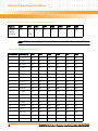
MVME3100 Single Board Computer Installation and Use (6806800M28C)
27
Hardware Preparation and Installation
Table 1-3 Geographical Address Switch Assignments (continued)
Position
SW1
SW21
SW3
SW4
SW5
SW6
SW7
SW8
Factory
Setting
(Default)
OFF
OFF
PCI
mode
OFF
1
OFF
1
OFF
1
OFF
1
OFF
1
OFF
1
Note: 1SW2 has been configured to work in PCI-X mode only. The default setting is OFF.
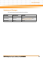
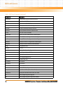
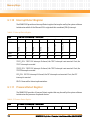
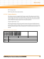
Table 1-4 Slot Geographical Address Settings
Slot Address
GAP GA(4:0)
SW3
SW4
SW5
SW6
SW7
SW8
1
1 11110
OFF
OFF
OFF
OFF
OFF
ON
2
1 11101
OFF
OFF
OFF
OFF
ON
OFF
3
0 11100
ON
OFF
OFF
OFF
ON
ON
4
1 11011
OFF
OFF
OFF
ON
OFF
OFF
5
0 11010
ON
OFF
OFF
ON
OFF
ON
6
0 11001
ON
OFF
OFF
ON
ON
OFF
7
1 11000
OFF
OFF
OFF
ON
ON
ON
8
1 10111
OFF
OFF
ON
OFF
OFF
OFF
9
0 10110
ON
OFF
ON
OFF
OFF
ON
10
0 10101
ON
OFF
ON
OFF
ON
OFF
11
1 10100
OFF
OFF
ON
OFF
ON
ON
12
0 10011
ON
OFF
ON
ON
OFF
OFF
13
1 10010
OFF
OFF
ON
ON
OFF
ON
14
1 10001
OFF
OFF
ON
ON
ON
OFF
15
0 10000
ON
OFF
ON
ON
ON
ON
16
1 01111
OFF
ON
OFF
OFF
OFF
OFF
17
0 01110
ON
ON
OFF
OFF
OFF
ON
18
0 01101
ON
ON
OFF
OFF
ON
OFF
19
1 01100
OFF
ON
OFF
OFF
ON
ON
28
MVME3100 Single Board Computer Installation and Use (6806800M28C)
Hardware Preparation and Installation
Table 1-4 Slot Geographical Address Settings (continued)
Slot Address
GAP GA(4:0)
SW3
SW4
SW5
SW6
SW7
SW8
20
0 01011
ON
ON
OFF
ON
OFF
OFF
21
1 01010
OFF
ON
OFF
ON
OFF
ON
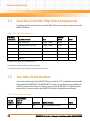
1.4.4
PMC I/O Voltage Configuration
The onboard PMC sites may be configured to support 3.3V or 5.0V I/O PMC modules. To
support 3.3V or 5.0V I/O PMC modules, both PMC I/O keying pins must be installed in the
holes. If both keying pins are not in the same location or if the keying pins are not installed, the
PMC sites will not function. Note that setting the PMC I/O voltage to 5.0V forces the PMC sites
to operate in PCI mode instead of PCI-X mode. The default factory configuration is for 3.3V
PMC I/O voltage.
1.4.5
RTM SEEPROM Address Switch (S1)
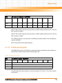
A 4-position SMT configuration switch is located on the RTM to set the device address of the
RTM serial EEPROM device. The switch settings are defined in the following table.
Table 1-5 RTM EEPROM Address Switch Assignments
Position
SW1
SW2
SW3
SW4
Function
A0
A1
A2
Not Used
OFF
1
1
1
Table 1-6 EEPROM Address Settings
Device Address
A(2:0)
SW1
SW2
SW3
$A0
000
ON
ON
ON
$A2
001
OFF
ON
ON
$A4
010
ON
OFF
ON
$A6
011
OFF
OFF
ON
$A8
100
ON
ON
OFF
$AA (Factory)
101
OFF
ON
OFF
MVME3100 Single Board Computer Installation and Use (6806800M28C)
29
Hardware Preparation and Installation
Table 1-6 EEPROM Address Settings (continued)
Device Address
A(2:0)
SW1
SW2
SW3
$AC
110
ON
OFF
OFF
$AE
111
OFF
OFF
OFF
The RTM EEPROM address switches must be set for address $AA in order for this device to be
accessible by MotLoad.
1.5
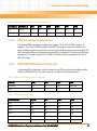
Installing Hardware
Damage of the Product and Additional Devices and Modules
z
Incorrect installation or removal of additional devices or modules may damage the
product or the additional devices or modules.
z
Before installing or removing additional devices or modules, read the respective
documentation.
Damage of Circuits
z
Electrostatic discharge and incorrect installation and removal of the product can
damage circuits or shorten their life.
z
Before touching the product make sure that your are working in an ESD-safe
environment or wear an ESD wrist strap or ESD shoes. Hold the product by its edges and
do not touch any components or circuits.
Product Malfunction
30
z
Switches marked as “Reserved” might carry production-related functions and can
cause the product to malfunction if their setting is changed.
z
Do not change settings of switches marked as “reserved”.
MVME3100 Single Board Computer Installation and Use (6806800M28C)
Hardware Preparation and Installation
Procedure
Use the following steps to install the MVME3100 into your computer chassis.
1. Attach an ESD strap to your wrist. Attach the other end of the ESD strap to an
electrical ground (refer to Unpacking Guidelines). The ESD strap must be secured to
your wrist and to ground throughout the procedure.
2. Remove any filler panel that might fill that slot.
3. Install the top and bottom edge of the MVME3100 into the guides of the chassis.
4. Ensure that the levers of the two injector/ejectors are in the outward position.
5. Slide the MVME3100 into the chassis until resistance is felt.
6. Simultaneously move the injector/ejector levers in an inward direction.
7. Verify that the MVME3100 is properly seated and secure it to the chassis using the
two screws located adjacent to the injector/ejector levers.
8. Connect the appropriate cables to the MVME3100.
To remove the board from the chassis, press the red locking tabs (IEEE handles only) and
reverse the procedure.
1.6
Connecting to Peripherals
When the MVME3100 is installed in a chassis, you are ready to connect peripherals and apply
power to the board.
MVME3100 Single Board Computer Installation and Use (6806800M28C)
31
Hardware Preparation and Installation
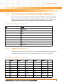
Figure 1-1 on page 25 shows the locations of the various connectors while Table 1-7 and Table
1-8 list them for you. Refer to Chapter 5, Pin Assignments for the pin assignments of the
connectors listed below.
Damage of the Product and Additional Devices and Modules
z
Incorrect installation or removal of additional devices or modules damages the product
or the additional devices or modules.
z
Before installing or removing additional devices or modules, read the respective
documentation and use appropriate tools.
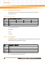
Table 1-7 MVME3100 Connectors
Connector
Function
J4
PMC expansion connector
J11, J12, J13, J14
PCI mezzanine card (PMC) slot 1 connector
J21, J22, J23
PCI mezzanine card (PMC) slot 2 connector
J24
Boundary scan header
J25
COP header
J27
USB connector
J28
Front panel sATA connector
J29
Planar sATA connector
J30
Planar sATA power connector
J41B
10/100/1000Mb/s Ethernet connector
J41A
COM port connector
P1, P2
VME backplane connectors
Table 1-8 MVME721 Rear Transition Module Connectors
Connector
Function
J1A, J1B, J1C, J1D
COM port connectors
32
MVME3100 Single Board Computer Installation and Use (6806800M28C)
Hardware Preparation and Installation
Table 1-8 MVME721 Rear Transition Module Connectors (continued)
Connector
Function
J2A
10/100/1000Mb/s Ethernet connector
J2B
10/100Mb/s Ethernet connector
J10
PIM power/ground
J14
PIM I/O
P2
VME backplane connector
1.7
Completing the Installation
Verify that hardware is installed and the power/peripheral cables connected are appropriate for
your system configuration.
Replace the chassis or system cover, reconnect the system to the AC or DC power source, and
turn the equipment power on.
MVME3100 Single Board Computer Installation and Use (6806800M28C)
33
Hardware Preparation and Installation
34
MVME3100 Single Board Computer Installation and Use (6806800M28C)
Chapter 2
Startup and Operation
2.1
Introduction
This chapter gives you information about the:
2.2
z
Power-up procedure
z
Runtime switches and indicators
Applying Power
After you verify that all necessary hardware preparation is complete and all connections are
made correctly, you can apply power to the system.
When you are ready to apply power to the MVME3100:
2.3
z
Verify that the chassis power supply voltage setting matches the voltage present in the
country of use (if the power supply in your system is not auto-sensing)
z
On powering up, the MVME3100 brings up the MOTLoad prompt, MVME3100>
Switches and Indicators
The MVME3100 board provides a single push button switch that provides both abort and reset
(ABT/RST) functions. When the switch is pressed for less than five seconds, an abort interrupt
is generated to the processor. If the switch is held for more than five seconds, a board hard reset
is generated. The board hard reset will reset the MPC8540, local PCI/PCI-X buses, Ethernet
PHYs, serial ports, Flash devices, and PLD(s). If the MVME3100 is configured as the VME system
controller, the VME bus and local TSi148 reset input are also reset.
The MVME3100 has four front-panel indicators. The following table describes these indicators:
Table 2-1 Front-Panel LED Status Indicators
Function
Label
Color
Description
Board Fail
FAIL
Yellow
Board has a failure. After Power On or reset, this
LED is ON until extinguished by firmware or
software.
User Defined
USER 1
Green
This indicator is illuminated by software
assertion of its corresponding register bit.
MVME3100 Single Board Computer Installation and Use (6806800M28C)
35
Startup and Operation
Table 2-1 Front-Panel LED Status Indicators (continued)
Function
Label
Color
Description
GENET 1 Link /
Speed
SPEED
Off
No link
Yellow
10/100Base-T operation
Green
1000Base-T operation
Blinking Green
Activity proportional to bandwidth utilization.
Off
No activity
GENET 1 Activity
36
ACT
MVME3100 Single Board Computer Installation and Use (6806800M28C)
Startup and Operation
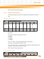
Figure 2-1
Front Panel LEDs and Connectors
PMC 2
PMC 1
SATA 1
ABORT/RESET
USER 1
COM 1
G ENET 1
FAIL
SPEED
ACT
MVME3100 Single Board Computer Installation and Use (6806800M28C)
37
Startup and Operation
The MVME721 rear transition module also has four status indicators. The following table
describes these indicators:
Table 2-2 MVME721 LED Status Indicators
Function
Label
Color
Description
GENET 2 Link/Speed
SPEED
Off
No link
Yellow
10/100Base-T operation
Green
1000Base-T operation
Blinking Green
Activity proportional to bandwidth utilization.
Off
No activity
Off
No link
Yellow
10/100Base-T operation
Blinking Green
Activity proportional to bandwidth utilization.
Off
No activity
GENET 2 Activity
ENET 1 Link/Speed
ENET 1 Activity
ACT
SPEED
ACT
Table 2-3 Additional Onboard Status Indicators
Function
Label
Color
Description
User
Defined LED
2
DS7
(silkscreen)
Green
This indicator is illuminated by software assertion of its
corresponding register bit.
User
Defined LED
3
DS8
(silkscreen)
Green
This indicator is illuminated by software assertion of its
corresponding register bit.
Power
Supply Fail
DS1
(silkscreen)
Red
This indicator is illuminated to indicate a power supply
fail condition.
sATA 0
Activity
DS4
(silkscreen)
Green
sATA 0 activity indicator
sATA 1
Activity
DS5
(silkscreen)
Green
sATA 1 activity indicator
38
MVME3100 Single Board Computer Installation and Use (6806800M28C)
Startup and Operation
Table 2-3 Additional Onboard Status Indicators (continued)
Function
Label
Color
Description
MPC8540
Ready
DS3
(silkscreen)
Green
Indicates that the MPC8540 has completed the reset
operation and is not in a power-down state. The
MPC8540 Ready is multiplexed with the MPC8540
TRIG_OUT so the LED can be programmed to indicate
one of three trigger events based on the value in the
MPC8540 TOSR register.
GENET 1
Link Quality
DS2
(silkscreen)
Off
Slow Blink
Green
Fast Blink Green
Green
Extremely poor Signal to Noise ratio - cannot receive data
Poor SNR - receive errors detected
Fair SNR - close to data error threshold
Good SNR on link
GENET 2
Link Quality
DS3
[Same as DS2}
MVME3100 Single Board Computer Installation and Use (6806800M28C)
39
Startup and Operation
40
MVME3100 Single Board Computer Installation and Use (6806800M28C)
Chapter 3
MOTLoad Firmware
3.1
Overview
The MOTLoad firmware package serves as a board power-up and initialization package, as well
as a vehicle from which user applications can be booted. A secondary function of the MOTLoad
firmware is to serve in some respects as a test suite providing individual tests for certain
devices. This chapter includes a list of standard MOTLoad commands, the default VME and
firmware settings that are changeable by the user, remote start, and the alternate boot
procedure.
MOTLoad is controlled through an easy-to-use, UNIX-like, command line interface. The
MOTLoad software package is similar to many end-user applications designed for the
embedded market, such as the real time operating systems currently available.
Refer to the MOTLoad Firmware Package User’s Manual, listed in Appendix B, Related
Documentation, for more details.
3.2
Implementation and Memory Requirements
The implementation of MOTLoad and its memory requirements are product specific. The
MVME3100 Single Board Computer (SBC) is offered with a wide range of memory (for
example, DRAM, external cache, flash). Typically, the smallest amount of on-board DRAM that
an Emerson SBC has is 32 MB. Each supported product line has its own unique MOTLoad binary
image(s). Currently the largest MOTLoad compressed image is less than 1 MB in size.
3.3
MOTLoad Commands
MOTLoad supports two types of commands (applications): utilities and tests. Both types of
commands are invoked from the MOTLoad command line in a similar fashion. Beyond that,
MOTLoad utilities and MOTLoad tests are distinctly different.
3.3.1
Utilities
The definition of a MOTLoad utility application is very broad. Simply stated, it is considered a
MOTLoad command, if it is not a MOTLoad test. Typically, MOTLoad utility applications are
applications that aid the user in some way (that is, they do something useful). From the
perspective of MOTLoad, examples of utility applications are: configuration, data/status
displays, data manipulation, help routines, data/status monitors, etc.
MVME3100 Single Board Computer Installation and Use (6806800M28C)
41
MOTLoad Firmware
Operationally, MOTLoad utility applications differ from MOTLoad test applications in several
ways:
3.3.2
z
Only one utility application operates at any given time (that is, multiple utility applications
cannot be executing concurrently)
z
Utility applications may interact with the user. Most test applications do not.
Tests
A MOTLoad test application determines whether or not the hardware meets a given standard.
Test applications are validation tests. Validation is conformance to a specification. Most
MOTLoad tests are designed to directly validate the functionality of a specific SBC subsystem
or component. These tests validate the operation of such SBC modules as: dynamic memory,
external cache, NVRAM, real time clock, etc.
All MOTLoad tests are designed to validate functionality with minimum user interaction. Once
launched, most MOTLoad tests operate automatically without any user interaction. There are
a few tests where the functionality being validated requires user interaction (that is, switch
tests, interactive plug-in hardware modules, etc.). Most MOTLoad test results (errordata/status-data) are logged, not printed. All MOTLoad tests/commands have complete and
separate descriptions (refer to the MOTLoad Firmware Package User’s Manual for this
information).
All devices that are available to MOTLoad for validation/verification testing are represented by
a unique device path string. Most MOTLoad tests require the operator to specify a test device
at the MOTLoad command line when invoking the test.
A listing of all device path strings can be displayed through the devShow command. If an SBC
device does not have a device path string, it is not supported by MOTLoad and can not be
directly tested. There are a few exceptions to the device path string requirement, like testing
RAM, which is not considered a true device and can be directly tested without a device path
string. Refer to the devShow command description page in the MOTLoad Firmware Package
User’s Manual.
42
MVME3100 Single Board Computer Installation and Use (6806800M28C)
MOTLoad Firmware
Most MOTLoad tests can be organized to execute as a group of related tests (a testSuite)
through the use of the testSuite command. The expert operator can customize their
testing by defining and creating a custom testSuite(s). The list of built-in and user-defined
MOTLoad testSuites, and their test contents, can be obtained by entering testSuite -d at
the MOTLoad prompt. All testSuites that are included as part of a product specific MOTLoad
firmware package are product specific. For more information, refer to the testSuite
command description page in the MOTLoad Firmware Package User’s Manual.
Test results and test status are obtained through the testStatus, errorDisplay, and
taskActive commands. Refer to the appropriate command description page in the
MOTLoad Firmware Package User’s Manual for more information.
3.3.3
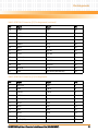
Command List
The following table provides a list of all current MOTLoad commands. Products supported by
MOTLoad may or may not employ the full command set. Typing help at the MOTLoad
command prompt will display all commands supported by MOTLoad for a given product.
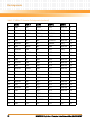
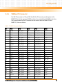
Table 3-1 MOTLoad Commands
Command
Description
as
One-Line Instruction Assembler
bcb
Block Compare Byte/Halfword/Word
bch
bcw
bdTempShow
Display Current Board Temperature
bfb
Block Fill Byte/Halfword/Word
bfh
bfw
blkCp
Block Copy
blkFmt
Block Format
blkRd
Block Read
blkShow
Block Show Device Configuration Data
blkVe
Block Verify
blkWr
Block Write
MVME3100 Single Board Computer Installation and Use (6806800M28C)
43
MOTLoad Firmware
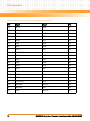
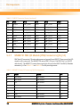
Table 3-1 MOTLoad Commands (continued)
Command
Description
bmb
Block Move Byte/Halfword/Word
bmh
bmw
br
Assign/Delete/Display User-Program Break-Points
bsb
Block Search Byte/Halfword/Word
bsh
bsw
bvb
Block Verify Byte/Halfword/Word
bvh
bvw
cdDir
ISO9660 File System Directory Listing
cdGet
ISO9660 File System File Load
clear
Clear the Specified Status/History Table(s)
cm
Turns on Concurrent Mode
csb
Calculates a Checksum Specified by Command-line Options
csh
csw
devShow
Display (Show) Device/Node Table
diskBoot
Disk Boot (Direct-Access Mass-Storage Device)
downLoad
Down Load S-Record from Host
ds
One-Line Instruction Disassembler
echo
Echo a Line of Text
elfLoader
ELF Object File Loader
errorDisplay
Display the Contents of the Test Error Status Table
eval
Evaluate Expression
execProgram
Execute Program
fatDir
FAT File System Directory Listing
fatGet
FAT File System File Load
44
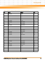
MVME3100 Single Board Computer Installation and Use (6806800M28C)
MOTLoad Firmware
Table 3-1 MOTLoad Commands (continued)
Command
Description
fdShow
Display (Show) File Discriptor
flashLock
Flash Memory Sector Lock
flashProgram
Flash Memory Program
flashShow
Display Flash Memory Device Configuration Data
flashUnlock
Flash Memory Sector Unlock
gd
Go Execute User-Program Direct (Ignore Break-Points)
gevDelete
Global Environment Variable Delete
gevDump
Global Environment Variable(s) Dump (NVRAM Header + Data)
gevEdit
Global Environment Variable Edit
gevInit
Global Environment Variable Area Initialize (NVRAM Header)
gevList
Global Environment Variable Labels (Names) Listing
gevShow
Global Environment Variable Show
gn
Go Execute User-Program to Next Instruction
go
Go Execute User-Program
gt
Go Execute User-Program to Temporary Break-Point
hbd
Display History Buffer
hbx
Execute History Buffer Entry
help
Display Command/Test Help Strings
l2CacheShow
Display state of L2 Cache and L2CR register contents
l3CacheShow
Display state of L3 Cache and L3CR register contents
mdb
Memory Display Bytes/Halfwords/Words
mdh
mdw
memShow
Display Memory Allocation
mmb
Memory Modify Bytes/Halfwords/Words
mmh
mmw
mpuFork
Execute program from idle processor
MVME3100 Single Board Computer Installation and Use (6806800M28C)
45
MOTLoad Firmware
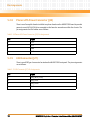
Table 3-1 MOTLoad Commands (continued)
Command
Description
mpuShow
Display multi-processor control structure
mpuStart
Start the other MPU
netBoot
Network Boot (BOOT/TFTP)
netShow
Display Network Interface Configuration Data
netShut
Disable (Shutdown) Network Interface
netStats
Display Network Interface Statistics Data
noCm
Turns off Concurrent Mode
pciDataRd
Read PCI Device Configuration Header Register
pciDataWr
Write PCI Device Configuration Header Register
pciDump
Dump PCI Device Configuration Header Register
pciShow
Display PCI Device Configuration Header Register
pciSpace
Display PCI Device Address Space Allocation
ping
Ping Network Host
portSet
Port Set
portShow
Display Port Device Configuration Data
rd
User Program Register Display
reset
Reset System
rs
User Program Register Set
set
Set Date and Time
sromRead
SROM Read
sromWrite
SROM Write
sta
Symbol Table Attach
stl
Symbol Table Lookup
stop
Stop Date and Time (Power-Save Mode)
taskActive
Display the Contents of the Active Task Table
tc
Trace (Single-Step) User Program
td
Trace (Single-Step) User Program to Address
46
MVME3100 Single Board Computer Installation and Use (6806800M28C)
MOTLoad Firmware
Table 3-1 MOTLoad Commands (continued)
Command
Description
testDisk
Test Disk
testEnetPtP
Ethernet Point-to-Point
testNvramRd
NVRAM Read
testNvramRdWr
NVRAM Read/Write (Destructive)
testRam
RAM Test (Directory)
testRamAddr
RAM Addressing
testRamAlt
RAM Alternating
testRamBitToggle
RAM Bit Toggle
testRamBounce
RAM Bounce
testRamCodeCopy
RAM Code Copy and Execute
testRamEccMonitor
Monitor for ECC Errors
testRamMarch
RAM March
testRamPatterns
RAM Patterns
testRamPerm
RAM Permutations
testRamQuick
RAM Quick
testRamRandom
RAM Random Data Patterns
testRtcAlarm
RTC Alarm
testRtcReset
RTC Reset
testRtcRollOver
RTC Rollover
testRtcTick
RTC Tick
testSerialExtLoop
Serial External Loopback
testSeriallntLoop
Serial Internal Loopback
testStatus
Display the Contents of the Test Status Table
testSuite
Execute Test Suite
testSuiteMake
Make (Create) Test Suite
testWatchdogTimer
Tests the Accuracy of the Watchdog Timer Device
tftpGet
TFTP Get
MVME3100 Single Board Computer Installation and Use (6806800M28C)
47
MOTLoad Firmware
Table 3-1 MOTLoad Commands (continued)
Command
Description
tftpPut
TFTP Put
time
Display Date and Time
transparentMode
Transparent Mode (Connect to Host)
tsShow
Display Task Status
upLoad
Up Load Binary Data from Target
version
Display Version String(s)
vmeCfg
Manages user specified VME configuration parameters
vpdDisplay
VPD Display
vpdEdit
VPD Edit
wait
Wait for Test Completion
waitProbe
Wait for I/O Probe to Complete
3.4
Using the Command Line Interface
Interaction with MOTLoad is performed via a command line interface through a serial port on
the SBC, which is connected to a terminal or terminal emulator (for example, Window’s
Hypercomm). The default MOTLoad serial port settings are: 9600 baud, 8 bits, no parity.
The MOTLoad command line interface is similar to a UNIX command line shell interface.
Commands are initiated by entering a valid MOTLoad command (a text string) at the MOTLoad
command line prompt and pressing the carriage-return key to signify the end of input.
MOTLoad then performs the specified action. An example of a MOTLoad command line
prompt is shown below. The MOTLoad prompt changes according to what product it is used on
(for example, MVME5500, MVME6100, MVME3100).
Example:
MVME3100>
If an invalid MOTLoad command is entered at the MOTLoad command line prompt, MOTLoad
displays a message that the command was not found.
Example:
48
MVME3100 Single Board Computer Installation and Use (6806800M28C)
MOTLoad Firmware
MVME3100> mytest
"mytest" not found
MVME3100>
If the user enters a partial MOTLoad command string that can be resolved to a unique valid
MOTLoad command and presses the carriage-return key, the command will be executed as if
the entire command string had been entered. This feature is a user-input shortcut that
minimizes the required amount of command line input. MOTLoad is an ever changing firmware
package, so user-input shortcuts may change as command additions are made.
Example:
MVME3100> version
Copyright: Motorola Inc.1999-2002, All Rights Reserved
MOTLoad RTOS Version 2.0
PAL Version 0.1 (Motorola MVME3100)
Example:
MVME3100> ver
Copyright: Motorola Inc. 1999-2002, All Rights Reserved
MOTLoad RTOS Version 2.0
PAL Version 0.1 (Motorola MVME3100)
If the partial command string cannot be resolved to a single unique command, MOTLoad will
inform the user that the command was ambiguous.
Example:
MVME3100> te
"te" ambiguous
MVME3100>
MVME3100 Single Board Computer Installation and Use (6806800M28C)
49
MOTLoad Firmware
3.4.1
Command Line Rules
There are a few things to remember when entering a MOTLoad command:
z
Multiple commands are permitted on a single command line, provided they are separated
by a single semicolon (;)
z
Spaces separate the various fields on the command line (command/arguments/options)
z
The argument/option identifier character is always preceded by a hyphen (-) character
z
Options are identified by a single character
z
Option arguments immediately follow (no spaces) the option
z
All commands, command options, and device tree strings are case sensitive
Example:
MVME3100> flashProgram –d/dev/flash0 –n00100000
For more information on MOTLoad operation and function, refer to the MOTLoad Firmware
Package User’s Manual.
3.4.2
Command Line Help
Each MOTLoad firmware package has an extensive, product-specific help facility that can be
accessed through the help command. The user can enter help at the MOTLoad command
line to display a complete listing of all available tests and utilities.
Example
MVME3100> help
For help with a specific test or utility the user can enter the following at the MOTLoad prompt:
help <command_name>
The help command also supports a limited form of pattern matching. Refer to the help
command page.
Example
MVME3100> help testRam
50
MVME3100 Single Board Computer Installation and Use (6806800M28C)
MOTLoad Firmware
Usage: testRam [-aPh] [-bPh] [-iPd] [-nPh] [-tPd] [-v]
Description: RAM Test [Directory]
Argument/Option Description
-a Ph: Address to Start (Default = Dynamic Allocation)
-b Ph: Block Size (Default = 16KB)
-i Pd: Iterations (Default = 1)
-n Ph: Number of Bytes (Default = 1MB)
-t Ph: Time Delay Between Blocks in OS Ticks (Default = 1)
-v O : Verbose Output
MVME3100>
3.5
Firmware Settings
The following sections provide additional information pertaining to the VME firmware settings
of the MVME3100. A few VME settings are controlled by hardware jumpers while the majority
of the VME settings are managed by the firmware command utility vmeCfg.
3.5.1
Default VME Settings
As shipped from the factory, the MVME3100 has the following VME configuration
programmed via Global Environment Variables (GEVs) for the Tsi148 VME controller. The
firmware allows certain VME settings to be changed in order for the user to customize the
environment. The following is a description of the default VME settings that are changeable by
the user. For more information, refer to the MOTLoad User’s Manual and Tundra’s Tsi148 User
Manual, listed in Appendix B, Related Documentation.
z
MVME3100>
vmeCfg -s -m
Displaying the selected Default VME Setting
- interpreted as follows:
VME PCI Master Enable [Y/N] = Y
MVME3100>
The PCI Master is enabled.
z
MVME3100> vmeCfg –s –r234
Displaying the selected Default VME Setting
- interpreted as follows:
VMEbus Master Control Register = 00000003
MVME3100>
MVME3100 Single Board Computer Installation and Use (6806800M28C)
51
MOTLoad Firmware
The VMEbus Master Control Register is set to the default (RESET) condition.
z
MVME3100> vmeCfg –s –r238
Displaying the selected Default VME Setting
- interpreted as follows:
VMEbus Control Register = 00000008
MVME3100>
The VMEbus Control Register is set to a Global Timeout of 2048 μseconds.
z
MVME3100> vmeCfg –s –r414
Displaying the selected Default VME Setting
- interpreted as follows:
CRG Attribute Register = 00000000
CRG Base Address Upper Register = 00000000
CRG Base Address Lower Register = 00000000
MVME3100>
The CRG Attribute Register is set to the default (RESET) condition.
z
MVME3100> vmeCfg –s –i0
Displaying the selected Default VME Setting
- interpreted as follows:
Inbound Image 0 Attribute Register = 000227AF
Inbound Image 0 Starting Address Upper Register = 00000000
Inbound Image 0 Starting Address Lower Register = 00000000
Inbound Image 0 Ending Address Upper Register = 00000000
Inbound Image 0 Ending Address Lower Register = 1FFF0000
Inbound Image 0 Translation Offset Upper Register = 00000000
Inbound Image 0 Translation Offset Lower Register = 00000000
MVME3100>
52
MVME3100 Single Board Computer Installation and Use (6806800M28C)
MOTLoad Firmware
Inbound window 0 (ITAT0) is not enabled; Virtual FIFO at 256 bytes, 2eSST timing at
SST320, respond to 2eSST, 2eVME, MBLT, and BLT cycles, A32 address space, respond to
Supervisor, User, Program, and Data cycles. Image maps from 0x00000000 to 0x1FFF0000
on the VMbus, translates 1x1 to the PCI-X bus (thus 1x1 to local memory). To enable this
window, set bit 31 of ITAT0 to 1.
For Inbound Translations, the Upper Translation Offset Register needs to be set to 0xFFFFFFFF to
ensure proper translations to the PCI-X Local Bus.
z
MVME3100> vmeCfg –s –o1
Displaying the selected Default VME Setting
- interpreted as follows:
Outbound Image 1 Attribute Register = 80001462
Outbound Image 1 Starting Address Upper Register = 00000000
Outbound Image 1 Starting Address Lower Register = 91000000
Outbound Image 1 Ending Address Upper Register = 00000000
Outbound Image 1 Ending Address Lower Register = AFFF0000
Outbound Image 1 Translation Offset Upper Register = 00000000
Outbound Image 1 Translation Offset Lower Register = 70000000
Outbound Image 1 2eSST Broadcast Select Register = 00000000
MVME3100>
Outbound window 1 (OTAT1) is enabled, 2eSST timing at SST320, transfer mode of 2eSST,
A32/D32 Supervisory access. The window accepts transfers on the PCI-X Local Bus from
0x91000000-0xAFFF0000 and translates them onto the VMEbus using an offset of
0x70000000, thus an access to 0x91000000 on the PCI-X Local Bus becomes an access to
0x01000000 on the VMEbus.
z
MVME3100> vmeCfg –s –o2
Displaying the selected Default VME Setting
- interpreted as follows:
Outbound Image 2 Attribute Register = 80001061
Outbound Image 2 Starting Address Upper Register
Outbound Image 2 Starting Address Lower Register
Outbound Image 2 Ending Address Upper Register =
Outbound Image 2 Ending Address Lower Register =
MVME3100 Single Board Computer Installation and Use (6806800M28C)
= 00000000
= B0000000
00000000
B0FF0000
53
MOTLoad Firmware
Outbound Image 2 Translation Offset Upper Register = 00000000
Outbound Image 2 Translation Offset Lower Register = 40000000
Outbound Image 2 2eSST Broadcast Select Register = 00000000
MVME3100>
Outbound window 2 (OTAT2) is enabled, 2eSST timing at SST320, transfer mode of SCT,
A24/D32 Supervisory access. The window accepts transfers on the PCI-X Local Bus from
0xB0000000-0xB0FF0000 and translates them onto the VMEbus using an offset of
0x40000000, thus an access to 0xB0000000 on the PCI-X Local Bus becomes an access to
0xF0000000 on the VMEbus.
z
MVME3100> vmeCfg –s –o3
Displaying the selected Default VME Setting
- interpreted as follows:
Outbound Image 3 Attribute Register = 80001061
Outbound Image 3 Starting Address Upper Register = 00000000
Outbound Image 3 Starting Address Lower Register = B3FF0000
Outbound Image 3 Ending Address Upper Register = 00000000
Outbound Image 3 Ending Address Lower Register = B3FF0000
Outbound Image 3 Translation Offset Upper Register = 00000000
Outbound Image 3 Translation Offset Lower Register = 4C000000
Outbound Image 3 2eSST Broadcast Select Register = 00000000
MVME3100>
Outbound window 3 (OTAT3) is enabled, 2eSST timing at SST320, transfer mode of SCT,
A16/D32 Supervisory access. The window accepts transfers on the PCI-X Local Bus from
0xB3FF0000-0xB3FF0000 and translates them onto the VMEbus using an offset of
0x4C000000, thus an access to 0xB3FF0000 on the PCI-X Local Bus becomes an access to
0xFFFF0000 on the VMEbus.
z
MVME3100> vmeCfg
–s
–o7
Displaying the selected Default VME Setting
- interpreted as follows:
Outbound Image 7 Attribute Register = 80001065
Outbound Image 7 Starting Address Upper Register
Outbound Image 7 Starting Address Lower Register
Outbound Image 7 Ending Address Upper Register =
Outbound Image 7 Ending Address Lower Register =
54
= 00000000
= B1000000
00000000
B1FF0000
MVME3100 Single Board Computer Installation and Use (6806800M28C)
MOTLoad Firmware
Outbound Image 7 Translation Offset Upper Register = 00000000
Outbound Image 7 Translation Offset Lower Register = 4F000000
Outbound Image 7 2eSST Broadcast Select Register = 00000000
MVME3100>
Outbound window 7 (OTAT7) is enabled, 2eSST timing at SST320, transfer mode of SCT,
CR/CSR Supervisory access. The window accepts transfers on the PCI-X Local Bus from
0xB1000000-0xB1FF0000 and translates them onto the VMEbus using an offset of
0x4F000000, thus an access to 0xB1000000 on the PCI-X Local Bus becomes an access to
0x00000000 on the VMEbus.
3.5.2
Control Register/Control Status Register Settings
The CR/CSR base address is initialized to the appropriate setting based on the Geographical
address; that is, the VME slot number. See the VME64 Specification and the VME64 Extensions
for details. As a result, a 512K byte CR/CSR area can be accessed from the VMEbus using the
CR/CSR AM code.
3.5.3
Displaying VME Settings
To display the changeable VME setting, type the following at the firmware prompt:
z
vmeCfg –s –m
Displays Master Enable state
z
vmeCfg –s –i(0 - 7)
Displays selected Inbound Window state
z
vmeCfg –s –o(0 - 7)
Displays selected Outbound Window state
z
vmeCfg –s –r184
Displays PCI Miscellaneous Register state
z
vmeCfg –s –r188
Displays Special PCI Target Image Register state
z
vmeCfg –s –r400
Displays Master Control Register state
z
vmeCfg –s –r404
Displays Miscellaneous Control Register state
MVME3100 Single Board Computer Installation and Use (6806800M28C)
55
MOTLoad Firmware
3.5.4
z
vmeCfg –s –r40C
Displays User AM Codes Register state
z
vmeCfg –s –rF70
Displays VMEbus Register Access Image Control Register state
Editing VME Settings
To edit the changeable VME setting, type the following at the firmware prompt:
56
z
vmeCfg –e –m
Edits Master Enable state
z
vmeCfg –e –i(0 - 7)
Edits selected Inbound Window state
z
vmeCfg –e –o(0 - 7)
Edits selected Outbound Window state
z
vmeCfg –e –r184
Edits PCI Miscellaneous Register state
z
vmeCfg –e –r188
Edits Special PCI Target Image Register state
z
vmeCfg –e –r400
Edits Master Control Register state
z
vmeCfg –e –r404
Edits Miscellaneous Control Register state
z
vmeCfg –e –r40C
Edits User AM Codes Register state
z
vmeCfg –e –rF70
Edits VMEbus Register Access Image Control Register state
MVME3100 Single Board Computer Installation and Use (6806800M28C)
MOTLoad Firmware
3.5.5
Deleting VME Settings
To delete the changeable VME setting (restore default value), type the following at the
firmware prompt:
3.5.6
z
vmeCfg –d –m
Deletes Master Enable state
z
vmeCfg –d –i(0 - 7)
Deletes selected Inbound Window state
z
vmeCfg –d –o(0 - 7)
Deletes selected Outbound Window state
z
vmeCfg –d –r184
Deletes PCI Miscellaneous Register state
z
vmeCfg –d –r188
Deletes Special PCI Target Image Register state
z
vmeCfg –d –r400
Deletes Master Control Register state
z
vmeCfg –d –r404
Deletes Miscellaneous Control Register state
z
vmeCfg –d –r40C
Deletes User AM Codes Register state
z
vmeCfg –d –rF70
Deletes VMEbus Register Access Image Control Register state
Restoring Default VME Settings
To restore all of the changeable VME setting back to their default settings, type the following
at the firmware prompt:
vmeCfg –z
MVME3100 Single Board Computer Installation and Use (6806800M28C)
57
MOTLoad Firmware
3.6
Remote Start
As described in the MOTLoad Firmware Package User's Manual, listed in Appendix B, Related
Documentation, remote start allows the user to obtain information about the target board,
download code and/or data, modify memory on the target, and execute a downloaded
program. These transactions occur across the VMEbus in the case of the MVME3100. MOTLoad
uses one of four mailboxes in the Tsi148 VME controller as the inter-board communication
address (IBCA) between the host and the target.
CR/CSR slave addresses configured by MOTLoad are assigned according to the installation slot
in the backplane, as indicated by the VME64 Specification. For reference, the following values
are provided:
Slot Position
CS/CSR Starting Address
1
0x0008.0000
2
0x0010.0000
3
0x0018.0000
4
0x0020.0000
5
0x0028.0000
6
0x0030.0000
7
0x0038.0000
8
0x0040.0000
9
0x0048.0000
A
0x0050.0000
B
0x0058.0000
C
0x0060.0000
For further details on CR/CSR space, please refer to the VME64 Specification, listed in Appendix
B, Related Documentation.
The MVME3100 uses a Discovery II for its VME bridge. The offsets of the mailboxes in the
Discovery II are defined in the Discovery II User Manual, listed in Appendix B, Related
Documentation, but are noted here for reference:
58
MVME3100 Single Board Computer Installation and Use (6806800M28C)
MOTLoad Firmware
Mailbox 0 is at offset 7f348 in the CR/CSR space
Mailbox 1 is at offset 7f34C in the CR/CSR space
Mailbox 2 is at offset 7f350 in the CR/CSR space
Mailbox 3 is at offset 7f354 in the CR/CSR space
The selection of the mailbox used by remote start on an individual MVME3100 is determined
by the setting of a global environment variable (GEV). The default mailbox is zero. Another GEV
controls whether remote start is enabled (default) or disabled. Refer to the Remote Start
appendix in the MOTLoad Firmware Package User's Manual for remote start GEV definitions.
The MVME3100’s IBCA needs to be mapped appropriately through the master’s VMEbus
bridge. For example, to use remote start using mailbox 0 on an MVME3100 installed in slot 5,
the master would need a mapping to support reads and writes of address 0x002ff348 in VME
CR/CSR space (0x280000 + 0x7f348).
3.7
Alternate Boot Images and Safe Start
Some later versions of MOTLoad support Alternate Boot Images and a Safe Start recovery
procedure. If Safe Start is available on the MVME3100, Alternate Boot Images are supported.
With Alternate Boot Image support, the bootloader code in the boot block examines the upper
8MB of the flash bank for Alternate Boot images. If an image is found, control is passed to the
image.
3.8
Firmware Startup Sequence Following Reset
The firmware startup sequence following reset of MOTLoad is to:
z
Initialize cache, MMU, FPU, and other CPU internal items
z
Initialize the memory controller
z
Search the active flash bank, possibly interactively, for a valid POST image. If found, the
POST images executes. Once completed, the POST image returns and startup continues.
z
Search the active flash bank, possibly interactively, for a valid USER boot image. If found,
the USER boot image executes. A return to the boot block code is not anticipated.
MVME3100 Single Board Computer Installation and Use (6806800M28C)
59
MOTLoad Firmware
z
If a valid USER boot image is not found, search the active flash bank, possibly interactively,
for a valid MCG boot image; anticipated to be upgrade of MCG firmware. If found, the
image is executed. A return to the boot block code is not anticipated.
z
Execute the recovery image of the firmware in the boot block if no valid USER or MCG
image is found
During startup, interactive mode may be entered by either setting the Safe Start
jumper/switch or by sending an <ESC> to the console serial port within five seconds of the
board reset. During interactive mode, the user has the option to display locations at which valid
boot images were discovered, specify which discovered image is to be executed, or specify that
the recovery image in the boot block of the active Flash bank is to be executed.
3.9
Firmware Scan for Boot Image
The scan is performed by examining each 1MB boundary for a defined set of flags that identify
the image as being Power On Self Test (POST), USER, or MCG. MOTLoad is an MCG image. POST
is a user-developed Power On Self Test that would perform a set of diagnostics and then return
to the bootloader image. User would be a boot image, such as the VxWorks bootrom, which
would perform board initialization. A bootable VxWorks kernel would also be a USER image.
Boot images are not restricted to being MB or less in size; however, they must begin on a 1MB
boundary within the 8MB of the scanned flash bank. The Flash Bank Structure is shown below:
Address
Usage
0xFFF00000 to 0xFFFFFFFF
Boot block. Recovery code
0xFFE00000 to 0XFFFFFFFF
Reserved for MCG use.
(MOTLoad update image)
0xFFD00000 to 0xFFDFFFFF
(FBD00000 or F7D00000)
First possible alternate image
(Bank B / Bank A actual)
0xFFC00000 to 0xFFCFFFFF
(FBC00000 or F7C00000)
Second possible alternate image
(Bank B / Bank A actual)
....
Alternate boot images
0xFF899999 to 0xFF8FFFFF
(Fb800000 or F3800000)
Last possible alternate image
(Bank B / Bank A actual)
60
MVME3100 Single Board Computer Installation and Use (6806800M28C)
MOTLoad Firmware
The scan is performed downwards from boot block image and searches first for POST, then
USER, and finally MCG images. In the case of multiple images of the same type, control is
passed to the first image encountered in the scan.
Safe Start, whether invoked by hitting ESC on the console within the first five seconds following
power-on reset or by setting the Safe Start jumper, interrupts the scan process. The user may
then display the available boot images and select the desired image. The feature is provided to
enable recovery in cases when the programmed Alternate Boot Image is no longer desired. The
following output is an example of an interactive Safe Start:
ABCDEInteractive Boot Mode Entered
boot> ?
Interactive boot commands:
'd':show directory of alternate boot images
'c':continue with normal startup
'q':quit without executing any alternate boot image
'r [address]':execute specified (or default) alternate image
'p [address]':execute specified (or default) POST image
'?':this help screen
'h':this help screen
boot> d
Addr FFE00000 Size 00100000 Flags 00000003 Name: MOTLoad
Addr FFD00000 Size 00100000 Flags 00000003 Name: MOTLoad
boot> c
NOPQRSTUVabcdefghijk#lmn3opqrsstuvxyzaWXZ
Copyright Motorola Inc. 1999-2004, All Rights Reserved
MOTLoad RTOS Version 2.0, PAL Version 0.b EA02
...
MVME3100>
MVME3100 Single Board Computer Installation and Use (6806800M28C)
61
MOTLoad Firmware
3.10
Boot Images
Valid boot images whether POST, USER, or MCG, are located on 1MB boundaries within flash.
The image may exceed 1MB in size. An image is determined valid through the presence of two
"valid image keys" and other sanity checks. A valid boot image begins with a structure as
defined in the following table:
Name
Type
Size
Notes
UserDefined
unsigned integer
8
User defined
ImageKey 1
unsigned integer
1
0x414c5420
ImageKey 2
unsigned integer
1
0x424f4f54
ImageChecksum
unsigned integer
1
Image checksum
ImageSize
unsigned integer
1
Must be a multiple of 4
ImageName
unsigned character
32
User defined
ImageRamAddress
unsigned integer
1
RAM address
ImageOffset
unsigned integer
1
Offset from header start to entry
ImageFlags
unsigned integer
1
Refer to Image Flags on page 63
ImageVersion
unsigned integer
1
User defined
Reserved
unsigned integer
8
Reserved for expansion
3.10.1 Checksum Algorithm
The checksum algorithm is a simple unsigned word add of each word (4 byte) location in the
image. The image must be a multiple of 4 bytes in length (word-aligned). The content of the
checksum location in the header is not part of the checksum calculation. The calculation
assumes the location to be zero. The algorithm is implemented using the following code:
Unsigned int checksum(
Unsigned int *startPtr,/* starting address */
Unsigned int endPtr/* ending address */
) {
unsigned int checksum=0;
while (startPtr < endPtr) {
checksum += *startPtr;
62
MVME3100 Single Board Computer Installation and Use (6806800M28C)
MOTLoad Firmware
startPtr++;
}
return(checksum);
}
3.10.2 Image Flags
The image flags of the header define various bit options that control how the image will be
executed.
Table 3-2 MOTLoad Image Flags
Name
Value
Interpretation
COPY_TO_RAM
0x00000001
Copy image to RAM at
ImageRamAddress
before execution
IMAGE_MCG
0x00000002
MCG-specific image
IMAGE_POST
0x00000004
POST image
DONT_AUTO_RUN
0x00000008
Image not to be executed
z
COPY_TO_RAM
If set, this flag indicates that the image is to be copied to RAM at the address specified in
the header before control is passed. If not set, the image will be executed in flash. In both
instances, control will be passed at the image offset specified in the header from the base
of the image.
z
IMAGE_MCG
If set, this flag defines the image as being an Alternate MOTLoad, as opposed to USER,
image. This bit should not be set by developers of alternate boot images.
z
IMAGE_POST
If set, this flag defines the image as being a power-on self-test image. This bit flag is used
to indicate that the image is a diagnostic and should be run prior to running either USER or
MCG boot images. POST images are expected, but not required, to return to the boot
block code upon completion.
MVME3100 Single Board Computer Installation and Use (6806800M28C)
63
MOTLoad Firmware
z
DONT_AUTO_RUN
If set, this flag indicates that the image is not to be selected for automatic execution. A
user, through the interactive command facility, may specify the image to be executed.
MOTLoad currently uses an Image Flag value of 0x3, which identifies itself as an Alternate
MOTLoad image that executes from RAM. MOTLoad currently does not support execution from
flash.
3.10.3 User Images
These images are user-developer boot code; for example, a VxWorks bootrom image. Such
images may expect the system software state to be as follows upon entry:
z
The MMU is disabled.
z
L1 instruction cache has been initialized and is enabled.
z
L1 data cache has been initialized (invalidated) and is disabled.
z
L2 cache is disabled.
z
L3 cache is disabled.
z
RAM has been initialized and is mapped starting at CPU address 0.
z
If RAM ECC or parity is supported, RAM has been scrubbed of ECC or parity errors.
z
The active Flash bank (boot) is mapped from the upper end of the address space.
z
If specified by COPY_TO_RAM, the image has been copied to RAM at the address specified
by ImageRamAddress.
z
CPU register R1 (the stack pointer) has been initialized to a value near the end of RAM.
z
CPU register R3 is added to the following structure:
typedef struct altBootData {
unsigned int ramSize;/* board's RAM size in MB */
void flashPtr;/* ptr to this image in flash */
char boardType[16];/* name string, eg MVME3100 */
void globalData;/* 16K, zeroed, user defined */
unsigned int reserved[12];
} altBootData_t;
64
MVME3100 Single Board Computer Installation and Use (6806800M28C)
MOTLoad Firmware
3.10.4 Alternate Boot Data Structure
The globalData field of the alternate boot data structure points to an area of RAM which was
initialized to zeroes by the boot loader. This area of RAM is not cleared by the boot loader after
execution of a POST image, or other alternate boot image, is executed. It is intended to provide
a user a mechanism to pass POST image results to subsequent boot images.
The boot loader performs no other initialization of the board than that specified prior to the
transfer of control to either a POST, USER, or MCG image. Alternate boot images need to
initialize the board to whatever state the image may further require for its execution.
POST images are expected, but not required, to return to the boot loader. Upon return, the
boot loader proceeds with the scan for an executable alternate boot image. POST images that
return control to the boot loader must ensure that upon return, the state of the board is
consistent with the state that the board was in at POST entry. USER images should not return
control to the boot loader.
3.10.5 Alternate Boot Images and Safe Start
Some later versions of MOTLoad support alternate boot images and a safe start recovery
procedure. If safe start is available on the MVME3100, alternate boot images are supported.
With alternate boot image support, the boot loader code in the boot block examines the upper
8 MB of the flash bank for alternate boot images. If an image is found, control is passed to the
image.
MVME3100 Single Board Computer Installation and Use (6806800M28C)
65
MOTLoad Firmware
3.10.6 Boot Image Firmware Scan
The scan is performed by examining each 1 MB boundary for a defined set of flags that identify
the image as being POST, USER, or Alternate MOTLoad. POST is a user-developed Power On Self
Test that would perform a set of diagnostics and then return to the boot loader image. USER
would be a boot image, such as the VxWorks bootrom, which would perform board
initialization. A bootable VxWorks kernel would also be a USER image. Boot images are not
restricted to being 1 MB or less in size; however, they must begin on a 1 MB boundary within
the 8 MB of the scanned flash bank. The flash bank structure is shown below:
Address
Usage
0xFFF00000 to 0xFFFFFFFF
Boot block. Recovery code.
0xFFE00000 to 0XFFFFFFFF
Backup MOTLoad image
0xFFD00000 to 0xFFDFFFFF
First possible alternate image
0xFFC00000 to 0xFFCFFFFF
Second possible alternate image
....
Alternate boot images
0xFF899999 to 0xFF8FFFFF
Bottom of flash (flash size varies per product)
The scan is performed downwards beginning at the location of the first possible alternate
image and searches first for POST, then USER, and finally Alternate MOTLoad images. In the
case of multiple images of the same type, control is passed to the first image encountered in
the scan.
Safe Start, whether invoked by hitting ESC on the console within the first five seconds following
power-on reset or by setting the Safe Start jumper, interrupts the scan process. The user may
then display the available boot images and select the desired image. The feature is provided to
enable recovery in cases when the programmed Alternate Boot Image is no longer desired. The
following output is an example of an interactive Safe Start:
ABCDEInteractive Boot Mode Entered
boot> ?
Interactive boot commands:
'd':show directory of alternate boot images
'c':continue with normal startup
'q':quit without executing any alternate boot image
'r [address]':execute specified (or default) alternate image
'p [address]':execute specified (or default) POST image
'?':this help screen
66
MVME3100 Single Board Computer Installation and Use (6806800M28C)
MOTLoad Firmware
'h':this help screen
boot> d
Addr FFE00000 Size 00100000 Flags 00000003 Name: MOTLoad
Addr FFD00000 Size 00100000 Flags 00000003 Name: MOTLoad
boot> c
NOPQRSTUVabcdefghijk#lmn3opqrsstuvxyzaWXZ
Copyright Motorola Inc. 1999-2004, All Rights Reserved
MOTLoad RTOS Version 2.0, PAL Version 0.b EA02
...
MVME3100>
3.11
Startup Sequence
The firmware startup sequence following reset of MOTLoad is to:
z
Initialize cache, MMU, FPU, and other CPU internal items
z
Initialize the memory controller
z
Search the active flash bank, possibly interactively, for a valid Power On Self Test (POST)
image. If found, the POST images executes. Once completed, the POST image returns and
startup continues.
z
Search the active flash bank, possibly interactively, for a valid USER boot image. If found,
the USER boot image executes. A return to the boot block code is not anticipated.
z
If a valid USER boot image is not found, search the active flash bank, possibly interactively,
for a valid Alternate MOTLoad boot image; anticipated to be an upgrade of alternate
MOTLoad firmware. If found, the image is executed. A return to the boot block code is not
anticipated.
z
Execute the recovery image of the firmware in the boot block if no valid USER or alternate
MOTLoad image is found
During startup, interactive mode may be entered by either setting the Safe Start
jumper/switch or by sending an <ESC> to the console serial port within five seconds of the
board reset. During interactive mode, the user has the option to display locations at which valid
boot images were discovered, specify which discovered image is to be executed, or specify that
the recovery image in the boot block of the active flash bank is to be executed.
MVME3100 Single Board Computer Installation and Use (6806800M28C)
67
MOTLoad Firmware
68
MVME3100 Single Board Computer Installation and Use (6806800M28C)
Chapter 4
Functional Description
4.1
Overview
This chapter describes the MVME3100 and the MVME721 rear transition module (RTM) on a
block diagram level.
4.2
Features
The following tables list the features of the MVME3100 and its RTM.
Table 4-1 MVME3100 Features Summary
Feature
Description
Processor/Host
Controller/Memory Controller
— Single 833 MHz MPC8540 PowerQUICC III™ integrated processor
(e500 core)
— Integrated 256KB L2 cache/SRAM
— Integrated four-channel DMA controller
— Integrated PCI/PCI-X controller
— Two integrated 10/100/1000 Ethernet controllers
— Integrated 10/100 Ethernet controller
— Integrated dual UART
— Integrated I2C controller
— Integrated programmable interrupt controller
— Integrated local bus controller
— Integrated DDR SDRAM controller
System Memory
— One SODIMM socket
— Up to DDR333, ECC
— One or two banks of memory on a single SODIMM
I2C Interface
— One 8KB VPD serial EEPROM
— Two 64KB user configuration serial EEPROMs
— One real-time clock (RTC) with removable battery
— One temperature sensor
— Interface to SPD(s) on SODIMM and P2 for RTM VPD
Flash
— 128MB soldered Flash with two alternate 1MB boot sectors selectable
via a hardware switch
— Hardware switch or software bit write protection for entire logical bank
MVME3100 Single Board Computer Installation and Use (6806800M28C)
69
Functional Description
Table 4-1 MVME3100 Features Summary (continued)
Feature
Description
PCI Interface
Bus A:
— 66 MHz PCI-X mode
— One TSi148 VMEbus controller
— One serial ATA (sATA) controller
— One MPC8540
— Two PCI6520 PCI-X-to-PCI-X bridges (primary side)
Bus B:
— 33/66/100 MHz PCI/PCI-X (PCI 2.2 and PCI-X 1.0b compliant)
— Two +3.3V/5V selectable VIO, 64-bit, single-wide PMC sites or one
double-wide PMC site (PrPMC ANSI/VITA 32-2003 and PCI-X Auxiliary
ANSI/VITA 39-2003 compliant)
— One PCI6520 PCI-X-to-PCI-X bridge (secondary side)
Bus C (-1263 version):
— 33 MHz PCI (PCI 2.2 compliant)
— One USB 2.0 controller
— One PCI expansion connector for interface to PMCspan
— One PCI6520 PCI-X-to-PCI-X bridge (secondary side)
I/O
— One front panel RJ45 connector with integrated LEDs for front I/O: one
serial channel
— One front panel RJ45 connector with integrated LEDs for front I/O: one
10/100/1000 Ethernet channel
— One front panel external sATA data connector for front I/O: one sATA
channel
— One front panel USB Type A upright receptacle for front I/O: one USB
2.0 channel (-1263 version)
— PMC site 1 front I/O and rear P2 I/O
— PMC site 2 front I/O
Serial ATA
— One four-channel sATA controller: one channel for front-panel I/O, one
channel for planar I/O, one channel for future rear P0 I/O, and one
channel is not used
— One planar data connector and one planar power connector for an
interface to the sATA hard disk drive
USB (-1263 version)
— One four-channel USB 2.0 controller: one channel for front panel
Ethernet
— Two 10/100/1000 MPC8540 Ethernet channels for front-panel I/O and
rear P2 I/O
— One 10/100 MPC8540 Ethernet channel for rear P2 I/O
70
MVME3100 Single Board Computer Installation and Use (6806800M28C)
Functional Description
Table 4-1 MVME3100 Features Summary (continued)
Feature
Description
Serial Interface
— One 16550-compatible, 9.6 to 115.2 KBAUD, MPC8540, asynchronous
serial channel for front-panel I/O
— One quad UART controller to provide four 16550-compatible, 9.6 to
115.2 KBAUD, asynchronous serial channels for rear P2 I/O
Timers
— Four 32-bit MPC8540 timers
— Four 32-bit timers in a PLD
Watchdog Timer
— One MPC8540 watchdog timer
VME Interface
— VME64 (ANSI/VITA 1-1994) compliant
— VME64 Extensions (ANSI/VITA 1.1-1997) compliant
— 2eSST (ANSI/VITA 1.5-2003) compliant
— VITA 41.0, version 0.9 compliant
— Two five-row P1 and P2 backplane connectors
— One TSi148 VMEbus controller
Form Factor
— Standard 6U VME
Miscellaneous
— One front-panel reset/abort switch
— Four front-panel status indicators: 10/100/1000 Ethernet link/speed
and activity, board fail, and user software controlled LED
— Six planar status indicators: one power supply status LED, two user
software controlled LEDs, three sATA activity LEDs (one per channel)
— One standard 16-pin COP header
— Boundary scan support
— Switches for VME geographical addressing in a three-row backplane
Software Support
— VxWorks operating system
— Linux operating system
Table 4-2 MVME721 RTM Features Summary
Feature
Description
I/O
— One five-row P2 backplane connector for serial and Ethernet I/O
passed from the MVME3100
— Four RJ-45 connectors for rear-panel I/O: four asynchronous serial
channels
— Two RJ-45 connectors with integrated LEDs for rear panel I/O: one
10/100/1000 Ethernet channel and one 10/100 Ethernet channel
— One PIM site with rear-panel I/O
MVME3100 Single Board Computer Installation and Use (6806800M28C)
71
Functional Description
Table 4-2 MVME721 RTM Features Summary (continued)
Feature
Description
Miscellaneous
— Four status indicators: 10/100/1000 and 10/100 Ethernet link/speed
and activity LEDs
72
MVME3100 Single Board Computer Installation and Use (6806800M28C)
Functional Description
4.3
Block Diagrams
Figure 4-1 shows a block diagram of the overall board architecture and Figure 4-2 shows a
block diagram of the MVME721 rear transition module architecture.
Figure 4-1
MVME3100 Block Diagram
MVME3100 Single Board Computer Installation and Use (6806800M28C)
73
Functional Description
Figure 4-2
MVME721 RTM Block Diagram
Rear Panel
Future Option
U
S
B
PIM 10
GigE
RJ45
sATA
10/100
RJ45
Serial
RJ45
Serial
RJ45
Serial
RJ45
Serial
RJ45
PIM
GigE 2
10/100
PMC 1 Jn4 10
Serial Port 4
Serial Port 3
Serial Port 2
Serial Port 1
VPD
8K8
sATA 3
USB 2
I2C
Bus
P2
P0
Future Option
4390 0106
4.4
Processor
The MVME3100 supports the MPC8540 processor. The processor core frequency runs at 833
or 667 MHz. The MPC8540 has integrated 256KB L2 cache.
4.5
System Memory
The MPC8540 provides one standard DDR SDRAM SODIMM socket. This socket supports
standard single or dual bank, unbuffered, SSTL-2 DDR-I, JESD8-9B compliant, SODIMM module
with ECC. The MPC8540 DDR memory interface supports up to 166 MHz (333 MHz data rate)
operation.
74
MVME3100 Single Board Computer Installation and Use (6806800M28C)
Functional Description
4.6
Local Bus Interface
The MVME3100 uses the MPC8540 local bus controller (LBC) for access to on-board Flash and
I/O registers. The LBC has programmable timing modes to support devices of different access
times, as well as device widths of 8, 16, and 32 bits.
The MVME3100 uses the LBC in GPCM (general purpose chip select machine) mode to
interface to two physical banks of on-board Flash, an on-board quad UART (QUART), on-board
32-bit timers, and the System Control/Status registers. Refer to the MVME3100 Single-Board
Computer Programmer’s Reference Guide listed in Appendix B, Related Documentation, for the
LBC bank and chip select assignments.
4.6.1
Flash Memory
The MVME3100 provides one physical bank of soldered-on Flash memory. The bank is
composed of two physical Flash devices configured to operate in 16-bit mode to form a 32-bit
Flash bank. The default configuration for the MVME3100-1263 is 128MB using two 512Mb
devices, and for the MVME3100-1152 it is 64MB using two 256Mb devices.
Refer to the MVME3100 Single-Board Computer Programmer’s Reference Guide listed in
Appendix B, Related Documentation, for more information.
4.6.2
Control and Timers Logic
The MVME3100 control and timers logic resides on the local bus. This logic provides the
following functions on the board:
z
Local bus address latch
z
Chip selects for Flash banks and QUART
z
System Control and Status registers
z
Four 32-bit tick timers
z
Real-time clock (RTC) 1 MHz reference clock
Refer to the MVME3100 Single-Board Computer Programmer’s Reference Guide listed in Appendix
B, Related Documentation, for more information.
MVME3100 Single Board Computer Installation and Use (6806800M28C)
75
Functional Description
4.7
I2C Serial Interface and Devices
The MVME3100 provides the following on-board I2C serial devices connected to the MPC8540
I2C controller interface:
z
8KB serial EEPROM for VPD
z
Two 64KB serial EEPROMs for user configuration data storage
z
256 byte serial EEPROM on SODIMM for SPD
z
Maxim DS1375 RTC
z
Maxim DS1621 temperature sensor
z
8KB serial EEPROM on RTM VPD
The Maxim DS1375 RTC implemented on the MVME3100 provides an alarm interrupt routed
to the MPC8540 programmable interrupt controller (PIC). A Maxim DS32KHz temperature
controlled crystal oscillator provides the RTC reference. A battery backup circuit for the RTC is
provided on board.
The Maxim DS1621 digital temperature sensor provides a measure of the temperature of the
board.
The I2C interface is also routed to the on-board SODIMM socket. This allows the serial presence
detect (SPD) in the serial EEPROM, which is located on the memory module, to be read and
used to configure the memory controller accordingly. Similarly, the I2C interface is routed to
the P2 connector for access to the serial EEPROM located on the RTM. The device address for
the RTM serial EERPOM is user-selectable using configuration switches on the RTM.
Refer to the MVME3100 Single-Board Computer Programmer’s Reference Guide in Appendix B,
Related Documentation, for more information.
4.8
Ethernet Interfaces
The MVME3100 provides one 10/100 and two 10/100/1000 Mb/s full duplex Ethernet
interfaces using the MPC8540 Fast Ethernet Controller (FEC) and two Triple Speed Ethernet
Controllers (TSEC). A Broadcom BCM5461S PHY is used for each TSEC interface, and each TSEC
interface and PHY is configured to operate in GMII mode. One Gigabit Ethernet interface is
routed to a front-panel RJ-45 connector with integrated LEDs for speed and activity indication.
The other Gigabit Ethernet interface is routed to P2 for rear I/O.
76
MVME3100 Single Board Computer Installation and Use (6806800M28C)
Functional Description
A Broadcom BCM5221 PHY is used for the FEC interface. The Fast Ethernet interface is routed
to P2 for rear I/O. Isolation transformers are provided on-board for each interface. The assigned
PHY addresses for the MPC8540 MII management (MIIM) interface can be found in the
MVME3100 Single-Board Computer Programmer’s Reference Guide, listed in Appendix B,
Related Documentation.
Each Ethernet interface is assigned an Ethernet Station Address. The address is unique for each
device. The Ethernet Station Addresses are displayed on labels attached to the PMC front-panel
keep-out area.
4.9
Asynchronous Serial Ports
The MVME3100 board contains one front-access asynchronous serial port interface using serial
port 0 from the MPC8540 dual UART (DUART) device. This serial port is routed to the RJ-45
front-panel connector.
This board also contains one quad UART (QUART) device connected to the MPC8540 device
controller bus to provide additional asynchronous serial ports. The QUART provides four
asynchronous serial ports,
SP1 — SP4, which are routed to the P2 connector. Refer to the ST16C554D Datasheet listed in
Appendix B, Related Documentation, for additional details and/or programming information.
4.10
PCI/PCI-X Interfaces and Devices
The MVME3100 provides three separate PCI/PCI-X bus segments. Bus segment A operates in
66MHz PCI-X mode and is connected to the MPC8540, the Tsi148 VME controller, the serial ATA
(sATA) controller, and two PCI-X-to-PCI-X bridges. Bus segment B is bridged between bus A and
the two PMC sites and operates in 33/66 MHz PCI or 66/100 MHz PCI-X mode depending on
the slowest speed PMC installed. Bus segment C is bridged between bus A, the USB controller,
and the PMCspan connector. Bus C operates at 33 MHz PCI mode.
4.10.1 MPC8540 PCI-X Interface
The MPC8540 PCI-X controller is configured to operate in PCI-X mode only, host bridge mode.
Bus A mode switch must be in "OFF" position in order to be fixed in PCI-X mode. The mode
cannot be changed by software. Refer to the MPC8540 Reference Manual listed in Appendix B,
Related Documentation, for additional details and/or programming information.
MVME3100 Single Board Computer Installation and Use (6806800M28C)
77
Functional Description
4.10.2 TSi148 VME Controller
The VMEbus interface for the MVME3100 is provided by the TSi148 ASIC. The TSi148 provides
the required VME, VME extensions, and 2eSST functions. Transceivers are used to buffer the
VME signals between the TSi148 and the VME backplane. Refer to the TSi148 User's Manual
listed in Appendix B, Related Documentation, for additional details and/or programming
information.
4.10.3 Serial ATA Host Controller
The sATA host controller uses the Silicon Image SiI3124A PCI-X to Serial ATA Controller. This
device provides four sATA channels at 1.5Gb/s and is compliant with the Serial ATA: High speed
serialized AT Attachment Specification, Revision 1.0. It also supports the native command
queuing feature of sATA II.
The MVME3100 uses two of the four sATA channels. Channel 0 is routed to a sATA connector
mounted on the front panel for an external drive connection. Channel 1 is routed to a planar
sATA connector for an "inside the chassis" drive connection. Collocated with the planar
connector is a sATA power connector. The sATA controller can operate in legacy (Native PCI
IDE) and Direct Port Access (DPA) mode.
The MVME3100 provides two programmable LEDs to indicate sATA channel activity.
Refer to the SiI3124A PCI-X to Serial ATA Controller Datasheet listed in Appendix B, Related
Documentation, for additional details and/or programming information
4.10.4 PCI-X-to-PCI-X Bridges
The MVME3100 uses two PLX PCI6520 PCI-X-to-PCI-X bridges to isolate the primary PCI bus,
bus A. These bridges isolate bus A from bus B with the PMC sites and from bus C with the USB
controller and PMCspan interface. The PCI6520 is a 64-bit, 133 MHz, PCI-X r1.0b compliant
device. It operates asynchronously between 33 MHz and 133 MHz on either primary or
secondary port. Refer to the PCI6520CB Data Book listed in Appendix B, Related
Documentation, for additional details and/or programming information.
78
MVME3100 Single Board Computer Installation and Use (6806800M28C)
Functional Description
4.10.5 PCI Mezzanine Card Slots
The MVME3100 provides two PMC sites that support standard PMCs or PrPMCs. Both PMC sites
are located on PCI bus B and operate at the same speed and mode as determined by the
slowest PMC module. The board routing supports a maximum of 100 MHz PCI-X operation on
each site. Signaling voltage (Vio) for the two PMC sites is dependent on keying pin installation
options and can be configured for 5V or 3.3V. Both sites must be configured for the same Vio
voltage or the Vio voltage will be disabled. Each PMC site has enough 3.3V and 5V power
allocated to support a 25 watt (max) PMC or PrPMC from either supply.
PMC slot 1 supports:
Feature
Description
Mezzanine Type:
PMC = PCI Mezzanine Card
Mezzanine Size:
S1B = Single width and standard depth
(75mm x 150mm) with front panel
PMC Connectors:
J11, J12, J13, and J14 (32/64-bit PCI with front and rear I/O)
Signaling Voltage:
VIO = +3.3V (+5V tolerant) or +5V, selected by keying pin
PMC slot 2 supports:
Feature
Description
Mezzanine Type:
PMC = PCI Mezzanine Card
Mezzanine Size:
S1B = Single width and standard depth
(75mm x 150mm) with front panel
PMC Connectors:
J21, J22, and J23 (32/64-bit PCI with front I/O)
Signalling Voltage:
VIO = +3.3V (+5V tolerant) or +5V, selected by keying pin
You cannot use 3.3V and 5V PMCs together; the voltage keying pin on slots 1 and 2 must be
identical. When in 5V mode, the bus runs at 33 MHz.
In addition, the PMC connectors are located such that a double-width PMC may be installed in
place of the two single-width PMCs.
MVME3100 Single Board Computer Installation and Use (6806800M28C)
79
Functional Description
In this case, the MVME3100 supports:
Feature
Description
Mezzanine Type:
PMC = PCI Mezzanine Card
Mezzanine Size:
Double width and standard depth
(150mm x 150mm) with front panel
PMC Connectors:
J11, J12, J13, J14, J21, J22, and J23
(32/64-bit PCI with front and rear I/O) on J14 only
Signaling Voltage:
VIO = +3.3V (+5V tolerant) or +5V, selected by keying pin
On PMC site 1, the user I/O — J14 signals will only support the low-current, high-speed signals
and are not to be used for any current bearing power supply usage. The maximum current
rating of each pin/signal is 100 mA.
4.10.6 USB
The USB 2.0 host controller provides USB ports with integrated transceivers for connectivity
with any USB-compliant device or hub. USB channel 1 is routed to a single USB connector
located at the front panel. DC power to the front panel USB port is supplied via a USB power
switch, which provides soft-start, current limiting, over-current detection, and power enable
for port 1. Refer to the μPD720101 USB 2.0 Host Controller Datasheet listed in Appendix B,
Related Documentation, for additional details.
4.10.7 PMC Expansion
The MVM3E3100 provides additional PMC module capability through the use of a connector
on bus C that is compatible with the PMCspan boards. Up to four additional PMC modules may
be added by using existing PMCspan boards. Refer to the PMCspan PMC Adapter Carrier Board
Installation and Use manual listed in Appendix B, Related Documentation, for additional details.
80
MVME3100 Single Board Computer Installation and Use (6806800M28C)
Functional Description
4.11
General-Purpose Timers
There are a total of eight independent, 32-bit timers. Four timers are integrated into the
MPC8540 and four timers are in the PLD. The four MPC8540 timers are clocked by the RTC
input, which is driven by a 1 MHz clock. The clock source for the four timers in the PLD is 25
MHz. Refer to the MPC8540 Reference Manual listed in Appendix B, Related Documentation, for
additional details and/or programming information.
4.12
Real-time Clock Battery
There is an on-board Renata SMT battery holder on the MVME3100. This SMTU2430-1 holder
allows for quick and easy replacement of a 3V button cell lithium battery (CR2430), which
provides back-up power to the on-board DS1375 RTC. A battery switching circuit provides
automatic switching between the 3.3V and battery voltages. The battery provides backup
power to the RTC for a minimum of one year at nominal temperature.
4.13
Reset Control Logic
The sources of reset on the MVME3100 are the following:
z
Power-up
z
Reset switch
z
Watchdog timer
z
System Control register bit
z
VMEbus reset
A board-level hard reset generates a reset for the entire board including the MPC8540, local
PCI/PCI-X buses, Ethernet PHYs, serial ports, Flash devices, and PLD(s). If the MVME3100 is
configured as the VME system controller, the VME bus and local TSi148 reset input are also
reset.
MVME3100 Single Board Computer Installation and Use (6806800M28C)
81
Functional Description
4.14
Debug Support
The MVME3100 provides a boundary scan header for boundary scan test access and device
programming. This board also provides a separate standard COP header for MPC8540 COP
emulation.
82
MVME3100 Single Board Computer Installation and Use (6806800M28C)
Chapter 5
Pin Assignments
5.1
Overview
This chapter provides pin assignments for various connectors and headers on the MMVE3100
single-board computer and the MVME721 transition module.
z
PMC Expansion Connector (J4)
z
Ethernet Connectors (GENET1/J41B, GENET2/J2B, ENET1/J2A)
z
PCI Mezzanine Card (PMC) Connectors (J11 — J14, J21 — J23)
z
Serial Port Connectors (COM1/J41A, COM2—COM5/J2A-D)
z
VMEbus P1 Connector
z
VMEbus P2 Connector
z
MVME721 PMC I/O Module (PIM) Connectors (J10, J14)
z
Planar sATA Power Connector (J30)
z
USB Connector (J27)
z
sATA Connectors (J28 and J29)
The following headers are described in this chapter:
5.2
z
Boundary Scan Header (J24)
z
Processor COP Header (J25)
Connectors
This section describes the pin assignments and signals for the connectors on the MVME3100.
MVME3100 Single Board Computer Installation and Use (6806800M28C)
83
Pin Assignments
5.2.1
PMC Expansion Connector (J4)
One 114-pin Mictor connector with a center row of power and ground pins is used to provide
PCI expansion capability. The pin assignments for this connector are as follows:
Table 5-1 PMC Expansion Connector (J4) Pin Assignments
Pin
Signal
Signal
Pin
1
+3.3V
+3.3V
2
3
PCICLK
PMCINTA#
4
5
GND
PMCINTB#
6
7
PURST#
PMCINTC#
8
9
HRESET#
PMCINTD#
10
11
TDO
TDI
12
13
TMS
TCK
14
15
TRST#
PEP#
16
17
PCIXGNT#
PCIXREQ#
18
19
+12V
-12V
20
21
PERR#
SERR#
22
23
LOCK#
No Connect
24
25
DEVSEL#
No Connect
26
27
GND
PCI XCAP
28
29
TRDY#
IRDY#
30
31
STOP#
FRAME#
32
33
GND
M66EN
34
35
ACK64#
No Connect
36
37
REQ64#
No Connect
38
84
GND
MVME3100 Single Board Computer Installation and Use (6806800M28C)
Pin Assignments
Table 5-1 PMC Expansion Connector (J4) Pin Assignments (continued)
Pin
Signal
Signal
Pin
39
PAR
PCIRST#
40
41
C/BE1#
C/BE0#
42
43
C/BE3#
C/BE2#
44
45
AD1
AD0
46
47
AD3
AD2
48
49
AD5
AD4
50
51
AD7
AD6
52
53
AD9
AD8
54
55
AD11
AD10
56
57
AD13
AD12
58
59
AD15
AD14
60
61
AD17
AD16
62
63
AD19
AD18
64
65
AD21
AD20
66
67
AD23
AD22
68
69
AD25
AD24
70
71
AD27
AD26
72
73
AD29
AD28
74
75
AD31
AD30
76
+5V
MVME3100 Single Board Computer Installation and Use (6806800M28C)
85
Pin Assignments
Table 5-1 PMC Expansion Connector (J4) Pin Assignments (continued)
Pin
Signal
Signal
Pin
77
PAR64
No Connect
78
79
C/BE5#
C/BE4#
80
81
C/BE7#
C/BE6#
82
83
AD33
AD32
84
85
AD35
AD34
86
87
AD37
AD36
88
89
AD39
AD38
90
91
AD41
AD40
92
93
AD43
AD42
94
95
AD45
AD44
96
97
AD47
AD46
98
99
AD49
AD48
100
101
AD51
AD50
102
103
AD53
AD52
104
105
AD55
AD54
106
107
AD57
AD56
108
109
AD59
AD58
110
111
AD61
AD60
112
113
AD63
AD62
114
GND
All PMC expansion signals are shared with the USB controller.
86
MVME3100 Single Board Computer Installation and Use (6806800M28C)
Pin Assignments
5.2.2
Ethernet Connectors (GENET1/J41B, GENET2/J2B, ENET1/J2A)
There is one 10/100 and two 10/100/1000Mb/s full duplex Ethernet interfaces using the
MPC8540 Fast Ethernet Controller (FEC) and two Triple Speed Ethernet Controllers (TSEC). One
Gigabit Ethernet interface is routed to a front-panel RJ-45 connector with integrated LEDs for
speed and activity indication. The other Gigabit Ethernet interface and the 10/100 interface
are routed to P2 for rear I/O. The pin assignments for these connectors are as follows:
Table 5-2 Ethernet Connectors Pin Assignment
Pin #
Signal
1000 Mb/s
10/100 Mb/s
1
MDIO0+
_DA+
TD+
2
MDIO0-
_DA-
TD-
3
MDIO1+
_DB+
RD+
4
MDIO1-
_DC+
Not Used
5
MDIO2+
_DC-
Not Used
6
MDIO2-
_DB-
RD-
7
MDIO3+
_DD+
Not Used
8
MDIO3-
_DD-
Not Used
5.2.3
PCI Mezzanine Card (PMC) Connectors (J11 — J14, J21 — J23)
There are seven 64-pin SMT connectors on the MVME3100 to provide 32/64-bit PCI interfaces
and P2 I/O for one optional add-on PMC.
PMC slot connector J14 contains the signals that go to VME P2 I/O rows A, C, D, and Z.
The pin assignments for these connectors are as follows.
Table 5-3 PMC Slot 1 Connector (J11) Pin Assignments
Pin
Signal
Signal
Pin
1
TCK
-12V
2
3
GND
INTA#
4
5
INTB#
INTC#
6
MVME3100 Single Board Computer Installation and Use (6806800M28C)
87
Pin Assignments
Table 5-3 PMC Slot 1 Connector (J11) Pin Assignments (continued)
Pin
Signal
Signal
Pin
7
PMCPRSNT1#
+5V
8
9
INTD#
PCI_RSVD
10
11
GND
+3.3Vaux
12
13
CLK
GND
14
15
GND
PMCGNT1#
16
17
PMCREQ1#
+5V
18
19
+3.3V (VIO)
AD31
20
21
AD28
AD27
22
23
AD25
GND
24
25
GND
C/BE3#
26
27
AD22
AD21
28
29
AD19
+5V
30
31
+3.3V (VIO)
AD17
32
33
FRAME#
GND
34
35
GND
IRDY#
36
37
DEVSEL#
+5V
38
39
GND
LOCK#
40
41
PCI_RSVD
PCI_RSVD
42
43
PAR
GND
44
45
+3.3V (VIO)
AD15
46
47
AD12
AD11
48
49
AD09
+5V
50
51
GND
C/BE0#
52
53
AD06
AD05
54
55
AD04
GND
56
57
+3.3V (VIO)
AD03
58
59
AD02
AD01
60
88
MVME3100 Single Board Computer Installation and Use (6806800M28C)
Pin Assignments
Table 5-3 PMC Slot 1 Connector (J11) Pin Assignments (continued)
Pin
Signal
Signal
Pin
61
AD00
+5V
62
63
GND
REQ64#
64
Table 5-4 PMC Slot 1 Connector (J12) Pin Assignments
Pin
Signal
Signal
Pin
1
+12V
TRST#
2
3
TMS
TDO
4
5
TDI
GND
6
7
GND
Not Used
8
9
Not Used
Not Used
10
11
Pull-up
+3.3V
12
13
RST#
Pull-down
14
15
+3.3V
Pull-down
16
17
Not Used
GND
18
19
AD30
AD29
20
21
GND
AD26
22
23
AD24
+3.3V
24
25
IDSEL1
AD23
26
27
+3.3V
AD20
28
29
AD18
GND
30
31
AD16
C/BE2#
32
33
GND
IDSEL1B
34
35
TRDY#
+3.3V
36
37
GND
STOP#
38
39
PERR#
GND
40
41
+3.3V
SERR#
42
43
C/BE1#
GND
44
MVME3100 Single Board Computer Installation and Use (6806800M28C)
89
Pin Assignments
Table 5-4 PMC Slot 1 Connector (J12) Pin Assignments (continued)
Pin
Signal
Signal
Pin
45
AD14
AD13
46
47
M66EN
AD10
48
49
AD08
+3.3V
50
51
AD07
REQ1B#
52
53
+3.3V
GNT1B#
54
55
Not Used
GND
56
57
Not Used
EREADY0
58
59
GND
Not Used
60
61
ACK64#
+3.3V
62
63
GND
No Connect (MONARCH#)
64
Table 5-5 PMC Slot 1 Connector (J13) Pin Assignments
Pin
Signal
Signal
Pin
1
Reserved
GND
2
3
GND
C/BE7#
4
5
C/BE6#
C/BE5#
6
7
C/BE4#
GND
8
9
+3.3V (VIO)
PAR64
10
11
AD63
AD62
12
13
AD61
GND
14
15
GND
AD60
16
17
AD59
AD58
18
19
AD57
GND
20
21
+3.3V (VIO)
AD56
22
23
AD55
AD54
24
25
AD53
GND
26
27
GND
AD52
28
90
MVME3100 Single Board Computer Installation and Use (6806800M28C)
Pin Assignments
Table 5-5 PMC Slot 1 Connector (J13) Pin Assignments (continued)
Pin
Signal
Signal
Pin
29
AD51
AD50
30
31
AD49
GND
32
33
GND
AD48
34
35
AD47
AD46
36
37
AD45
GND
38
39
+3.3V (VIO)
AD44
40
41
AD43
AD42
42
43
AD41
GND
44
45
GND
AD40
46
47
AD39
AD38
48
49
AD37
GND
50
51
GND
AD36
52
53
AD35
AD34
54
55
AD33
GND
56
57
+3.3V (VIO)
AD32
58
59
Reserved
Reserved
60
61
Reserved
GND
62
63
GND
Reserved
64
Table 5-6 PMC Slot 1 Connector (J14) Pin Assignments
Pin
Signal
Signal
Pin
1
PMC1_1 (P2-C1)
PMC1_2 (P2-A1)
2
3
PMC1_3 (P2-C2)
PMC1_4 (P2-A2)
4
5
PMC1_5 (P2-C3)
PMC1_6 (P2-A3)
6
7
PMC1_7 (P2-C4)
PMC1_8 (P2-A4)
8
9
PMC1 _9 (P2-C5)
PMC1_10 (P2-A5)
10
11
PMC1_11 (P2-C6)
PMC1_12 (P2-A6)
12
MVME3100 Single Board Computer Installation and Use (6806800M28C)
91
Pin Assignments
Table 5-6 PMC Slot 1 Connector (J14) Pin Assignments (continued)
Pin
Signal
Signal
Pin
13
PMC1_13 (P2-C7)
PMC1_14 (P2-A7)
14
15
PMC1_15 (P2-C8)
PMC1_16 (P2-A8)
16
17
PMC1_17 (P2-C9)
PMC1_18 (P2-A9)
18
19
PMC1_19 (P2-C10)
PMC1_20 (P2-A10)
20
21
PMC1PMC1_21 (P2-C11)
PMC1_22 (P2-A11)
22
23
PMC1_23 (P2-C12)
PMC1_24 (P2-A12)
24
25
PMC1_25 (P2-C13)
PMC1_26 (P2-A13)
26
27
PMC1_27 (P2-C14)
PMC1_28 (P2-A14)
28
29
PMC1_29 (P2-C15)
PMC1_30 (P2-A15)
30
31
PMC1_31 (P2-C16)
PMC1_32 (P2-A16)
32
33
PMC1_33 (P2-C17)
PMC1_34 (P2-A17)
34
35
PMC1_35 (P2-C18)
PMC1_36 (P2-A18)
36
37
PMC1_37 (P2-C19)
PMC1_38 (P2-A19)
38
39
PMC1_39 (P2-C20)
PMC1_40 (P2-A20)
40
41
PMC1_41 (P2-C21)
PMC1_42 (P2-A21)
42
43
PMC1_43 (P2-C22)
PMC1_44 (P2-A22)
44
45
PMC1_45 (P2-C23)
PMC1_46 (P2-A23)
46
47
PMC1_47 (P2-C24)
PMC1_48 (P2-A24)
48
49
PMC1_49 (P2-C25)
PMC1_50 (P2-A25)
50
51
PMC1_51 (P2-C26)
PMC1_52 (P2-A26)
52
53
PMC1_53 (P2-C27)
PMC1_54 (P2-A27)
54
55
PMC1_55 (P2-C28)
PMC1_56 (P2-A28)
56
57
PMC1_57 (P2-C29)
PMC1_58 (P2-A29)
58
59
PMC1_59 (P2-C30)
PMC1_60 (P2-A30)
60
61
PMC1_61 (P2-C31)
PMC1_62 (P2-A31)
62
63
PMC1_63 (P2-C32)
PMC1_64 (P2-A32)
64
92
MVME3100 Single Board Computer Installation and Use (6806800M28C)
Pin Assignments
Table 5-7 PMC Slot 2 Connector (J21) Pin Assignments
Pin
Signal
Signal
Pin
1
TCK
-12V
2
3
GND
INTC#
4
5
INTD#
INTA#
6
7
PMCPRSNT1#
+5V
8
9
INTB#
PCI_RSVD
10
11
GND
+3.3Vaux
12
13
CLK
GND
14
15
GND
PMCGNT1#
16
17
PMCREQ1#
+5V
18
19
+3.3V (VIO)
AD31
20
21
AD28
AD27
22
23
AD25
GND
24
25
GND
C/BE3#
26
27
AD22
AD21
28
29
AD19
+5V
30
31
+3.3V (VIO)
AD17
32
33
FRAME#
GND
34
35
GND
IRDY#
36
37
DEVSEL#
+5V
38
39
GND
LOCK#
40
41
PCI_RSVD
PCI_RSVD
42
43
PAR
GND
44
45
+3.3V (VIO)
AD15
46
47
AD12
AD11
48
49
AD09
+5V
50
51
GND
C/BE0#
52
53
AD06
AD05
54
MVME3100 Single Board Computer Installation and Use (6806800M28C)
93
Pin Assignments
Table 5-7 PMC Slot 2 Connector (J21) Pin Assignments (continued)
Pin
Signal
Signal
Pin
55
AD04
GND
56
57
+3.3V (VIO)
AD03
58
59
AD02
AD01
60
61
AD00
+5V
62
63
GND
REQ64#
64
Table 5-8 PMC Slot 2 Connector (J22) Pin Assignments
Pin
Signal
Signal
Pin
1
+12V
TRST#
2
3
TMS
TDO
4
5
TDI
GND
6
7
GND
Not Used
8
9
Not Used
Not Used
10
11
Pull-up
+3.3V
12
13
RST#
Pull-down
14
15
+3.3V
Pull-down
16
17
Not Used
GND
18
19
AD30
AD29
20
21
GND
AD26
22
23
AD24
+3.3V
24
25
IDSEL1
AD23
26
27
+3.3V
AD20
28
29
AD18
GND
30
31
AD16
C/BE2#
32
33
GND
IDSEL1B
34
35
TRDY#
+3.3V
36
37
GND
STOP#
38
94
MVME3100 Single Board Computer Installation and Use (6806800M28C)
Pin Assignments
Table 5-8 PMC Slot 2 Connector (J22) Pin Assignments (continued)
Pin
Signal
Signal
Pin
39
PERR#
GND
40
41
+3.3V
SERR#
42
43
C/BE1#
GND
44
45
AD14
AD13
46
47
M66EN
AD10
48
49
AD08
+3.3V
50
51
AD07
REQ1B#
52
53
+3.3V
GNT1B#
54
55
Not Used
GND
56
57
Not Used
EREADY1
58
59
GND
Not Used
60
61
ACK64#
+3.3V
62
63
GND
No Connect (MONARCH#)
64
Table 5-9 PMC Slot 2 Connector (J23) Pin Assignments
Pin
Signal
Signal
Pin
1
Reserved
GND
2
3
GND
C/BE7#
4
5
C/BE6#
C/BE5#
6
7
C/BE4#
GND
8
9
+3.3V (VIO)
PAR64
10
11
AD63
AD62
12
13
AD61
GND
14
15
GND
AD60
16
17
AD59
AD58
18
19
AD57
GND
20
21
+3.3V (VIO)
AD56
22
MVME3100 Single Board Computer Installation and Use (6806800M28C)
95
Pin Assignments
Table 5-9 PMC Slot 2 Connector (J23) Pin Assignments (continued)
Pin
Signal
Signal
Pin
23
AD55
AD54
24
25
AD53
GND
26
27
GND
AD52
28
29
AD51
AD50
30
31
AD49
GND
32
33
GND
AD48
34
35
AD47
AD46
36
37
AD45
GND
38
39
+3.3V (VIO)
AD44
40
41
AD43
AD42
42
43
AD41
GND
44
45
GND
AD40
46
47
AD39
AD38
48
49
AD37
GND
50
51
GND
AD36
52
53
AD35
AD34
54
55
AD33
GND
56
57
+3.3V (VIO)
AD32
58
59
Reserved
Reserved
60
61
Reserved
GND
62
63
GND
Reserved
64
96
MVME3100 Single Board Computer Installation and Use (6806800M28C)
Pin Assignments
5.2.4
Serial Port Connectors (COM1/J41A, COM2—COM5/J2A-D)
There is one front access asynchronous serial port interface (SP0) that is routed to the RJ-45
front-panel connector. There are four asynchronous serial port interfaces, SP1 — SP4, which are
routed to the P2 connector. The pin assignments for these connectors are as follows:
Table 5-10 COM Port Connector Pin Assignments
Pin
Signal
1
No connect
2
RTS
3
GND
4
TX
5
RX
6
GND
7
CTS
8
No connect
5.2.5
VMEbus P1 Connector
The VME P1 connector is a 160-pin DIN. The P1 connector provides power and VME signals for
24-bit address and 16-bit data. The pin assignments for the P1 connector is as follows:
Table 5-11 VMEbus P1 Connector Pin Assignments
ROW Z
ROW A
ROW B
ROW C
ROW D
1
Reserved
D00
BBSY*
D08
+5V
1
2
GND
D01
BCLR*
D09
GND
2
3
Reserved
D02
ACFAIL*
D10
Reserved
3
4
GND
D03
BG0IN*
D11
Reserved
4
5
Reserved
D04
BG0OUT*
D12
Reserved
5
6
GND
D05
BG1IN*
D13
Reserved
6
7
Reserved
D06
BG1OUT*
D14
Reserved
7
MVME3100 Single Board Computer Installation and Use (6806800M28C)
97
Pin Assignments
Table 5-11 VMEbus P1 Connector Pin Assignments (continued)
ROW Z
ROW A
ROW B
ROW C
ROW D
8
GND
D07
BG2IN*
D15
Reserved
8
9
Reserved
GND
BG2OUT*
GND
GAP_L
9
10
GND
SYSCLK
BG3IN*
SYSFAIL*
GA0_L
10
11
Reserved
GND
BG3OUT*
BERR*
GA1_L
11
12
GND
DS1*
BR0*
SYSRESET*
Reserved
12
13
Reserved
DS0*
BR1*
LWORD*
GA2_L
13
14
GND
WRITE*
BR2*
AM5
Reserved
14
15
Reserved
GND
BR3*
A23
GA3_L
15
16
GND
DTACK*
AM0
A22
Reserved
16
17
Reserved
GND
AM1
A21
GA4_L
17
18
GND
AS*
AM2
A20
Reserved
18
19
Reserved
GND
AM3
A19
Reserved
19
20
GND
IACK*
GND
A18
Reserved
20
21
Reserved
IACKIN*
SERA
A17
Reserved
21
22
GND
IACKOUT*
SERB
A16
Reserved
22
23
Reserved
AM4
GND
A15
Reserved
23
24
GND
A07
IRQ7*
A14
Reserved
24
25
Reserved
A06
IRQ6*
A13
Reserved
25
26
GND
A05
IRQ5*
A12
Reserved
26
27
Reserved
A04
IRQ4*
A11
Reserved
27
28
GND
A03
IRQ3*
A10
Reserved
28
29
Reserved
A02
IRQ2*
A09
Reserved
29
30
GND
A01
IRQ1*
A08
Reserved
30
31
Reserved
-12V
+5VSTDBY
+12V
GND
31
32
GND
+5V
+5V
+5V
+5V
32
98
MVME3100 Single Board Computer Installation and Use (6806800M28C)
Pin Assignments
5.2.6
VMEbus P2 Connector
The VME P2 connector is a 160-pin DIN. Row B of the P2 connector provides power to the
MVME3100 and to the upper eight VMEbus address lines and additional 16 VMEbus data lines.
The pin assignments for the P2 connector are the same for both the MVME3100 and
MVME721, and are as follows:
Table 5-12 VME P2 Connector Pinouts
Pin
P2-Z
P2-A
P2-B
P2-C
P2-D
1
SP1RX
PMC1_IO2
+5V
PMC1_IO1
E1-1+
2
GND
PMC1_IO4
GND
PMC1_IO3
E1-1-
3
SPITX
PMC1_IO6
VRETRY_L
PMC1_IO5
GND
4
GND
PMC1_IO8
VA24
PMC1_IO7
E1-2+
5
SP1CTS
PMC1_IO10
VA25
PMC1_IO9
E1-2-
6
GND
PMC1_IO12
VA26
PMC1_IO11
GND
7
SP1RTS
PMC1_IO14
VA27
PMC1_IO13
NC
8
GND
PMC1_IO16
VA28
PMC1_IO15
NC
9
SP2RX
PMC1_IO18
VA29
PMC1_IO17
GND
10
GND
PMC1_IO20
VA30
PMC1_IO19
NC
11
SP2TX
PMC1_IO22
VA31
PMC1_IO21
NC
12
GND
PMC1_IO24
GND
PMC1_IO23
GND
13
SP2CTS
PMC1_IO26
+5V
PMC1_IO25
I2C_SDA
14
GND
PMC1_IO28
VD16
PMC1_IO27
I2C_SCL
15
SP2RTS
PMC1_IO30
VD17
PMC1_IO29
E1_LINK
16
GND
PMC1_IO32
VD18
PMC1_IO31
E1_ACT
17
SP3RX
PMC1_IO34
VD19
PMC1_IO33
E2_LINK
18
GND
PMC1_IO36
VD20
PMC1_IO35
E2_ACT
19
SP3TX
PMC1_IO38
VD21
PMC1_IO37
GND
20
GND
PMC1_IO40
VD22
PMC1_IO39
E2-4-
21
SP3CTS
PMC1_IO42
VD23
PMC1_IO41
E2-4+
22
GND
PMC1_IO44
GND
PMC1_IO43
GND
MVME3100 Single Board Computer Installation and Use (6806800M28C)
99
Pin Assignments
Table 5-12 VME P2 Connector Pinouts (continued)
Pin
P2-Z
P2-A
P2-B
P2-C
P2-D
23
SP3RTS
PMC1_IO46
VD24
PMC1_IO45
E2-3-
24
GND
PMC1_IO48
VD25
PMC1_IO47
E2-3+
25
SP4RX
PMC1_IO50
VD26
PMC1_IO49
GND
26
GND
PMC1_IO52
VD27
PMC1_IO51
E2-2-
27
SP4TX
PMC1_IO54
VD28
PMC1_IO53
E2-2+
28
GND
PMC1_IO56
VD29
PMC1_IO55
GND
29
SP4CTS
PMC1_IO58
VD30
PMC1_IO57
E2-1-
30
GND
PMC1_IO60
VD31
PMC1_IO59
E2-1+
31
SP4RTS
PMC1_IO62
GND
PMC1_IO61
GND
32
GND
PMC1_IO64
+5V
PMC1_IO63
+5V
5.2.7
MVME721 PMC I/O Module (PIM) Connectors (J10, J14)
PMC Host I/O connector J10 routes only power and ground from VME P2. There are no Host I/O
signals on this connector. The MVME3100 routes PMC I/O from J14 of PMC Slot 1 to VME P2
rows A and C. The MVME721 routes these signals (pin-for-pin) from VME P2 to PMC I/O Module
connector J14. See Table 5-13 and Table 5-6 for the pin assignments.
Table 5-13 MVME721 Host I/O Connector (J10) Pin Assignments
Pin
Signal
Signal
Pin
1
No Connect
No Connect
2
3
No Connect
No Connect
4
5
+5V
No Connect
6
7
No Connect
No Connect
8
9
No Connect
+3.3V
10
11
No Connect
No Connect
12
13
GND
No Connect
14
15
No Connect
No Connect
16
100
MVME3100 Single Board Computer Installation and Use (6806800M28C)
Pin Assignments
Table 5-13 MVME721 Host I/O Connector (J10) Pin Assignments (continued)
Pin
Signal
Signal
Pin
17
No Connect
GND
18
19
No Connect
No Connect
20
21
+5V
No Connect
22
23
No Connect
No Connect
24
25
No Connect
+3.3V
26
27
No Connect
No Connect
28
29
GND
No Connect
30
31
No Connect
No Connect
32
33
No Connect
GND
34
35
No Connect
No Connect
36
37
+5V
No Connect
38
39
No Connect
No Connect
40
41
No Connect
+3.3V
42
43
No Connect
No Connect
44
45
GND
No Connect
46
47
No Connect
No Connect
48
49
No Connect
GND
50
51
No Connect
No Connect
52
53
+5V
No Connect
54
55
No Connect
No Connect
56
57
No Connect
+3.3V
58
59
No Connect
No Connect
60
61
No Connect
No Connect
62
63
No Connect
No Connect
64
MVME3100 Single Board Computer Installation and Use (6806800M28C)
101
Pin Assignments
5.2.8
Planar sATA Power Connector (J30)
There is one 2mm pitch header installed as a planar header on the MVME3100 board to provide
power to a serial ATA (sATA) drive mounted on the board or somewhere within the chassis. The
pin assignments for this header are as follows:
Table 5-14 Planar sATA Power Connector (J30) Pin Assignments
Pin
Signal
1
+5V
2
+5V
3
GND
4
GND
5.2.9
USB Connector (J27)
There is one USB Type A connector located on the MVME3100 front panel. The pin assignments
are as follows:
Table 5-15 USB Connector (J27) Pin Assignments
Pin
Signal
1
USB_VBUS (+5.0V)
2
USB_DATA-
3
USB_DATA+
4
GND
102
MVME3100 Single Board Computer Installation and Use (6806800M28C)
Pin Assignments
5.2.10 sATA Connectors (J28 and J29)
The MVME3100 has two sATA connectors. J28 is an internal type sATA connector located on the
planar and is intended to connect to a drive located on the board or somewhere inside the
chassis. J29 is an external type sATA connected located on the front panel and is intended to
connect to an external sATA drive. The pin assignment for these connectors is as follows:
Table 5-16 sATA Connectors (J28 and J29) Pin Assignments
Pin
Signal
1
GND
2
SATA_TX+
3
SATA_TX-
4
GND
5
SATA_RX-
6
SATA_RX+
7
GND
5.3
Headers
This section describes the pin assignments of the Headers on the MVME3100. For Hheader
settings, refer to Configuring Hardware on page 22.
5.3.1
Boundary Scan Header (J24)
The 14-pin boundary scan header provides an interface for programming the on-board PLDs
and for boundary scan testing/debug purposes. The pin assignments for this header are as
follows:
Table 5-17 Boundary Scan Header (J24) Pin Assignments
Pin
Signal
Signal
Pin
1
TRST_L
GND
2
3
TDO
GND
4
MVME3100 Single Board Computer Installation and Use (6806800M28C)
103
Pin Assignments
Table 5-17 Boundary Scan Header (J24) Pin Assignments (continued)
Pin
Signal
Signal
Pin
5
TDI
GND
6
7
TMS
GND
8
9
TCK
GND
10
11
NC
GND (BSCANEN_L)
12
13
BSCAN_AW_L
GND
14
Pin 12 must be grounded in the cable in order to enable boundary scan.
5.3.2
Processor COP Header (J25)
There is one standard 16-pin header that provides access to the COP function. The pin
assignments for this header are as follows:
Table 5-18 Processor COP Header (J25) Pin Assignments
Pin
Signal
Signal
Pin
1
CPU_TDO
No Connect
2
3
CPU_TDI
CPU_TRST_L
4
5
Pullup
CPU_VIO (+3.3V)
6
7
CPU_TCK
CPU_CKSTPI_L
8
9
CPU_TMS
No Connect
10
11
CPU_SRST_L
GND (optional pull-down)
12
13
CPU_HRST_L
KEY (no pin)
14
15
CPU_CKSTPO_L
GND
16
Pin 6 +3.3V has a resettable fuse and can supply up to 0.5A to power I/O buffers in the COP
controller.
104
MVME3100 Single Board Computer Installation and Use (6806800M28C)
Chapter 6
Memory Maps
6.1
Memory Maps
6.1.1
Default Processor Memory Map
The MPC8540 presents a default processor memory map following RESET negation. The
following table shows the default memory map from the point of view of the processor. The
e500 core only provides one default TLB entry to access boot code and it allows for accesses
within the highest 4KB of memory. To access the full 8MB of default boot space (and the 1MB
of CCSR space), additional TLB entries must be set up within the e500 core for mapping these
regions. Refer to the MPC8540 Reference Manual listed in Appendix B, Related Documentation,
for details.
This is the default location for the CCSRs, but it is not mapped after reset.
Table 6-1 Default Processor Address Map
Processor Address
Start
End
Size
Definition
Notes
0000 0000
FF6F FFFF
4087M
Not mapped
FF70 0000
FF7F FFFF
1M
MPC8540 CCS Registers
1
FF80 0000
FFFF FFFF
8M
Flash
2
Only FFFF F000 to FFFF FFFF is mapped after reset. The e500 core fetches the first instruction
from FFFF FFFC following a reset.
MVME3100 Single Board Computer Installation and Use (6806800M28C)
105
Memory Maps
6.1.2
MOTLoad’s Processor Memory Map
MOTLoad’s processor memory map is given in the following table.
Table 6-2 MOTLoad’s Processor Address Map
Processor Address
Start
End
Size
Definition
Notes
0000 0000
top_dram-1
dram_size
(2GB max)
System Memory (on-board DRAM)
8000 0000
DFFF FFFF
1.5GB
PCI Memory Space/VME
E000 0000
E0FF FFFF
16MB
PCI I/O Space
E100 0000
E10F FFFF
1MB
MPC8540 CCSR
E1100 0000
E1FF FFFF
15MB
Not Used
E200 0000
E2FF FFFF
16MB
Status/Control Registers/UARTs,
External Timers
E300 0000
EFFF FFFF
208MB
Not Used
F000 0000
F7FF FFFF
128MB
Reserved
1, 2
bottom_flash
FFFF FFFF
flash_size
(128MB max)
Flash
2
1. Reserved for future larger flash devices.
2. The flash is ligically one back but may be physically implemented in two banks.
After RESET, the MPC8540 does not map any PCI memory space (inbound or outbound), and
does not respond to Config cycles.
6.1.3
VME Memory Map
The MVME3100 is fully capable of supporting both the PReP and the CHRP VME Memory Map
examples with RAM size limited to 2GB.
106
MVME3100 Single Board Computer Installation and Use (6806800M28C)
Memory Maps
6.1.4
System I/O Memory Map
System resources including System Control and Status registers, external timers, and the
QUART are mapped into a 16MB address range from the MVME3100 via the MPC8540 local bus
controller (LBC). The memory map is defined in the following table, including the LBC bank chip
select used to decode the register:
Table 6-3 System I/O Memory Map
Address
Definition
LBC Bank /
Chip Select
Notes
E200 0000
System Status Register
2
3
E200 0001
System Control Register
2
3
E200 0002
Status Indicator Register
2
3
E200 0003
Flash Control/Status Register
2
3
E200 0004
PCI Bus A Status Register
2
3
E200 0005
PCI Bus B Status Register
2
3
E200 0006
PCI Bus C Status Register
2
3
E200 0007
Interrupt Detect Register
2
3
E200 0008
Presence Detect Register
2
3
E200 0009
PLD Revision
2
3
E200 000C
PLD Date Code (32 bits)
2
3
E200 0010
Test Register 1 (32 bits)
2
3
E200 0014
Test Register 2 (32 bits)
2
3
E200 0018 E200 0FFF
Reserved
E201 1000 E201 1FFF
COM 2 (QUART channel 1)
3
E201 2000 E201 2FFF
COM 3 (QUART channel 2)
3
E201 3000 E201 3FFF
COM 4 (QUART channel 3)
3
E201 4000 E201 4FFF
COM 5 (QUART channel 4)
3
MVME3100 Single Board Computer Installation and Use (6806800M28C)
1
107
Memory Maps
Table 6-3 System I/O Memory Map (continued)
LBC Bank /
Chip Select
Address
Definition
Notes
E201 5000 E201 FFFF
Reserved
E202 0000
External PLD Tick Timer Prescaler Register
4
2
E202 0010
External PLD Tick Timer 1 Control Register
4
2
E202 0014
External PLD Tick Timer 1 Compare Register
4
2
E202 0018
External PLD Tick Timer 1 Counter Register
4
2
E202 001C
Reserved
4
2
E202 0020
External PLD Tick Timer 2 Control Register
4
2
E202 0024
External PLD Tick Timer 2 Compare Register
4
2
E202 0028
External PLD Tick Timer 2 Counter Register
4
2
E202 002C
Reserved
4
2
E202 0030
External PLD Tick Timer 3 Control Register
4
2
E202 0034
External PLD Tick Timer 3 Compare Register
4
2
E202 0038
External PLD Tick Timer 3 Counter Register
4
2
E202 003C
Reserved
4
2
E202 0040
External PLD Tick Timer 4 Control Register
4
2
E202 0044
External PLD Tick Timer 4 Compare Register
4
2
E202 0048
External PLD Tick Timer 4 Counter Register
4
2
E202 004C - E2FF
FFFF
Reserved
1
1
1. Reserved for future implementation
2. 32-bit write only
3. Byte read/write capable
108
MVME3100 Single Board Computer Installation and Use (6806800M28C)
Memory Maps
6.1.5
System Status Register
The MVME3100 board System Status register is a read-only register used to provide board
status information.
System Status Register — 0xE2000000
BIT
7
6
5
4
3
2
RSVD
RSVD
SAFE_START
ABORT
RSVD
0
0
X
0
0
FIELD
OPER
R
RESET
0
1
0
BD_TYPE
REG
RSVD
Table 6-4 System Status Register
0
0
BD_TYPE
Board type. These bits indicate the board type.
00: VME SBC
01: PrPMC
10-11: Reserved
ABORT: This bit reflects the current state of the on-board abort signal. This is a debounced
version of the abort switch and may be used to determine the state of the abort switch. A
cleared condition indicates the abort switch is not depressed, while a set condition indicates
the abort switch is asserted.
SAFE_START: ENV safe start. This bit reflects the current state of the ENV safe start select
switch. A set condition indicates that firmware should use the safe ENV settings. A cleared
condition indicates that the ENV settings programmed in NVRAM should be used by the
firmware.
RSVD: Reserved for future implementation.
MVME3100 Single Board Computer Installation and Use (6806800M28C)
109
Memory Maps
6.1.6
System Control Register
The MVME3100 board System Control register provides board control bits.
Table 6-5 System Control Register
REG
System Control Register - 0xE2000001
BIT
7
6
5
4
3
2
1
0
0
0
TSTAT_MASK
0
EEPROM_WP
RESET
RSVD
R/W
RSVD
OPER
RSVD
BD_RESET
FIELD
R
R
R
R/W
R/W
0
0
X
1
1
TSTAT_MASK: Thermostat mask. This bit masks the DS1621 temperature sensor thermostat
output. If this bit is cleared, the thermostat output is enabled to generate an interrupt. If the
bit is set, the thermostat output is disabled from generating an interrupt.
EEPROM_WPEEPROM: Write protect. This bit provides protection against inadvertent writes
to the on-board EEPROM devices. Clearing this bit will enable writes to the EEPROM devices.
Setting this bit write protects the devices. The devices are write protected following a reset.
BRD_RST: Board reset. These bits force a hard reset of the board. If a pattern is written in bits
5-7 where bit 7 is set, bit 6 is cleared, and bit 5 is set (101), a hard reset is generated. Any other
pattern written in bits 5-7, does not generate a hard reset. These bits are cleared automatically
when the board reset has been completed. These bits are always cleared during a read.
RSVD: Reserved for future implementation.
110
MVME3100 Single Board Computer Installation and Use (6806800M28C)
Memory Maps
6.1.7
System Indicator Register
The MVME3100 board provides a System Indicator register that may be read by the system
software to determine the state of the on-board status indicator LEDs or written to by system
software to illuminate the corresponding on-board LEDs.
Table 6-6 System Indicator Register
REG
System Indicator Register - 0xE2000002
BIT
7
6
5
4
3
2
1
0
RSVD
RSVD
RSVD
RSVD
USR3
USR2
USR1
BRD_FAIL
FIELD
OPER
R
R
R
R
R/W
R/W
R/W
R/W
RESET
0
0
0
0
0
0
0
1
BRD_FAIL: Board fail. This bit controls the board fail LED located on the front panel. A set
condition illuminates the front-panel LED and a cleared condition extinguishes the front-panel
LED.
USR1_LED: User LED 1. This bit controls the USR1 LED located on the front panel. A set
condition illuminates the front-panel LED and a cleared condition extinguishes the front-panel
LED.
USR2_LED: User LED 2. This bit controls the planar USR2 LED. A set condition illuminates the
LED and a cleared condition extinguishes the LED.
USR3_LED: User LED 3. This bit controls the planar USR3 LED. A set condition illuminates the
LED and a cleared condition extinguishes the LED.
RSVD: Reserved for future implementation.
MVME3100 Single Board Computer Installation and Use (6806800M28C)
111
Memory Maps
6.1.8
Flash Control/Status Register
The MVME3100 provides software-controlled bank write protect and map select functions as
well as boot block select, bank write protect, and activity status for the Flash.
Table 6-7 Flash Control/Status Register
REG
Flash Control/Status Register - 0xE2000003
BIT
7
6
5
4
3
2
1
0
RSVD
RSVD
RSVD
MAP_SEL
F_WP_SW
F_WP_HW
FBT_BLK_SEL
FLASH_RDY
FIELD
OPER
R
R
R
R/W
R/W
R
R
R
RESET
0
0
0
0
1
X
X
1
FLASH_RDY: Flash ready. This bit provides the current state of the Flash devices’ Ready/Busy#
pins. These open drain output pins from each Flash device are wire OR'd to form Flash Ready.
FBT_BLK_SEL: Flash boot block select. This bit reflects the current state of the BOOT BLOCK B
SELECT switch. A cleared condition indicates that boot block A is selected and mapped to the
highest address. A set condition indicates that boot block B is selected and mapped to the
highest address.
F_WP_HW: Hardware Flash bank write protect switch status. This bit reflects the current state
of the FLASH BANK WP switch. A set condition indicates that the entire Flash bank is write
protected. A cleared condition indicates that the Flash bank is not write protected.
F_WP_SW: Software Flash bank write protect. This bit provides software-controlled
protection against inadvertent writes to the Flash memory devices. A set condition indicates
that the entire Flash is write-protected. A cleared condition indicates that the Flash bank is not
write-protected, only when the hardware write-protect bit is also not set. This bit is set during
reset and must be cleared by the system software to enable writing of the Flash devices.
MAP_SEL: Memory map select. When this bit is cleared, the Flash memory map is controlled
by the Flash Boot Block Select switch. When the map select bit is set, boot block A is selected
and mapped to the highest address.
112
MVME3100 Single Board Computer Installation and Use (6806800M28C)
Memory Maps
RSVD: Reserved for future implementation.
6.1.9
PCI Bus Status Registers
The PCI Bus Status registers provide PCI bus configuration information for each of the PCI
buses.
Table 6-8 PCI Bus A Status Register
PCI Bus A Status Register - 0xE2000004
BIT
7
6
5
4
3
2
0
RSVD
RSVD
RSVD
RSVD
PCI_A_64B
PCIX_A
FIELD
1
PCI_A_SPD
REG
OPER
R
R
R
R
R
R
R
R
RESET
0
0
0
0
1
X
0
1
PCI_A_SPD
PCI bus A speed. Indicates the frequency of PCI bus A.
00: 33 MHz
01: 66 MHz
10: 100 MHz
11: 133 MHz
PCIX_A: PCI-X bus A. A set condition indicates that bus A is operating in
PCI-X mode. A cleared condition indicates PCI mode.
PCI_A_64B: PCI bus A 64-bit. A set condition indicates that bus A is enabled to operate in 64bit mode. A cleared condition indicates 32-bit mode.
RSVD: Reserved for future implementation.
Table 6-9 PCI Bus B Status Register
REG
PCI Bus B Status Register - 0xE2000005
BIT
7
6
5
4
3
MVME3100 Single Board Computer Installation and Use (6806800M28C)
2
1
0
113
Memory Maps
Table 6-9 PCI Bus B Status Register (continued)
3.3V_VIO
5.0V_VIO
ERDY2
ERDY1
PCI_B_64B
PCIX_B
FIELD
PCI Bus B Status Register - 0xE2000005
PCI_B_SPD
REG
OPER
R
R
R
R
R
R
R
R
RESET
X
X
X
0
1
X
X
X
PCI_B_SPD:
PCI bus B speed. Indicates the frequency of PCI bus B.
00: 33 MHz
01: 66 MHz
10: 100 MHz
11: 133 MHz
PCIX_B: PCI-X bus B. A set condition indicates that bus B is operating in
PCI-X mode. A cleared condition indicates PCI mode.
PCI_B_64B: PCI bus B 64-bit. A set condition indicates that bus B is enabled to operate in 64bit mode. A cleared condition indicates 32-bit mode.
ERDY1: EREADY1. Indicates that the PrPMC module installed in PMC site 1 is ready for
enumeration when set. If cleared, the PrPMC module is not ready for enumeration. If no PrPMC
is installed, this bit is always set.
ERDY2: EREADY2. Indicates that the PrPMC module installed in PMC site 2 is ready for
enumeration when set. If cleared, the PrPMC module is not ready for enumeration. If no PrPMC
is installed, the bit is always set.
5.0V_VIO: 5.0V VIO Enabled. This bit set indicates that the PMC bus (PCI bus B) is configured
for 5.0V VIO.
114
MVME3100 Single Board Computer Installation and Use (6806800M28C)
Memory Maps
3.3V_VIO: 3.3V VIO enabled. This bit set indicates that the PMC bus (PCI bus B) is configured
to 3.3V VIO.
Table 6-10 PCI Bus C Status Register
PCI Bus C Status Register - 0xE2000006
BIT
7
6
5
4
3
2
0
RSVD
RSVD
RSVD
RSVD
PCI_C_64B
PCIX_C
FIELD
1
PCI_C_SPD
REG
OPER
R
R
R
R
R
R
R
R
RESET
X
X
X
0
1
X
X
X
PCI_C_SPD:
PCI bus C speed. Indicates the frequency of PCI bus C.
00: 33 MHz
01: 66 MHz
10: 100 MHz
11: 133 MHz
PCIX_C: PCI-X bus C. A set condition indicates that bus C is operating in
PCI-X mode. A cleared condition indicates PCI mode.
PCI_C_64B: PCI bus C 64-bit. A set condition indicates that bus C is enabled to operate in 64bit mode. A cleared condition indicates 32-bit mode.
RSVD: Reserved for future implementation.
MVME3100 Single Board Computer Installation and Use (6806800M28C)
115
Memory Maps
6.1.10 Interrupt Detect Register
The MVME3100 provides an Interrupt Detect register that may be read by the system software
to determine which of the Ethernet PHYs originated their combined (OR'd) interrupt.
Table 6-11 Interrupt Detect Register
REG
Interrupt Detect Register - 0xE2000007
BIT
7
6
5
4
3
2
1
0
RSVD
RSVD
RSVD
RSVD
RSVD
FEC_PHY
TSEC2_PHY
TSEC1_PHY
FIELD
OPER
R
R
R
R
R
R
R
R
RESET
1
1
1
0
0
0
0
0
TSEC1_PHY: TSEC1 PHY interrupt. If cleared, the TSEC1 interrupt is not asserted. If set, the
TSEC1 interrupt is asserted.
TSEC2_PHY: TSEC2 PHY interrupt. If cleared, the TSEC2 interrupt is not asserted. If set, the
TSEC2 interrupt is asserted.
FEC_PHY: FEC PHY interrupt. If cleared, the FEC interrupt is not asserted. If set, the FEC
interrupt is asserted.
RSVD: Reserved for future implementation.
6.1.11 Presence Detect Register
The MVME3100 provides a Presence Detect register that may be read by the system software
to determine the presence of optional devices.
Table 6-12 Presence Detect Register
REG
Presence Detect Register - 0xE2000008
BIT
7
116
6
5
4
3
2
1
0
MVME3100 Single Board Computer Installation and Use (6806800M28C)
Memory Maps
Table 6-12 Presence Detect Register (continued)
REG
RSVD
RSVD
RSVD
RSVD
RSVD
PEP
PMC2P
PMC1P
FIELD
Presence Detect Register - 0xE2000008
OPER
R
R
R
R
R
R
R
R
RESET
0
0
0
0
0
X
X
X
PMC1P: PMC module 1 present. If cleared, there is no PMC module installed in site 1. If set, the
PMC module is installed.
PMC2P: PMC module 2 present. If cleared, there is no PMC module installed in site 2. If set, the
PMC module is installed.
PEP: PMCspan present. If cleared, there is no PMCspan module installed. If set, the PMCspan
module is installed.
RSVD: Reserved for future implementation.
6.1.12 PLD Revision Register
The MVME3100 provides a PLD Revision register that may be read by the system software to
determine the current revision of the timers/registers PLD.
Table 6-13 PLD Revision Register
REG
PLD Revision Register - 0xE2000009
BIT
7
FIELD
PLD_REV
OPER
R
RESET
01
6
5
4
3
2
1
0
PLD_REV: 8-bit field containing the current timer/register PLD revision. The revision number
starts with 01.
MVME3100 Single Board Computer Installation and Use (6806800M28C)
117
Memory Maps
6.1.13 PLD Data Code Register
The MVME3100 PLD provides a 32-bit register that contains the build date code of the
timers/registers PLD.
Table 6-14 PLD Data Code Register
REG
PLD Data Code Register - 0xE200000C
BIT
31:24
23:16
15:8
7:0
FIELD
yy
mm
dd
vv
OPER
R/W
RESET
xxxx
yy: Last two digits of the year
mm: Month
dd: Day
vv: Version
6.1.14 Test Register 1
The MVME3100 provides a 32-bit general-purpose read/write register that can be used by
software for PLD test or general status bit storage.
Table 6-15 Test Register 1
REG
Test Register 1 - 0xE2000010
BIT
31:0
FIELD
TEST1
OPER
R/W
RESET
0000
TEST1: General-purpose 32-bit read/write field.
118
MVME3100 Single Board Computer Installation and Use (6806800M28C)
Memory Maps
6.1.15 Test Register 2
The MVME3100 provides a second 32-bit test register that reads back the complement of the
data in test register 1.
Table 6-16 Test Register 2
REG
Test Register 2 - 0xE2000014
BIT
31:0
FIELD
TEST2
OPER
R/W
RESET
FFFF
TEST2: A read from this address returns the complement of the data pattern in test register 1.
A write to this address writes the uncomplemented data to register TEST1.
6.1.16 External Timer Registers
The MVME3100 provides a set of tick timer registers for access to the four external timers
implemented in the timers/registers PLD. These registers are 32-bit registers and are not byte
writable. The following sections describe the external timer prescaler and control registers.
6.1.16.1 Prescalar Register
The prescaler provides the clock required by each of the four timers. The tick timers require a 1
MHz clock input. The input clock to the prescaler is 25 MHz. The default value is set for $E7,
which gives a 1 MHz reference clock for a 25 MHz input clock source.
Table 6-17 Prescalar Register
REG
Prescalar Register - 0xE2020000 (8 bits of 32)
BIT
7
FIELD
Prescalar Adjust
OPER
R/W
RESET
$E7
6
5
4
3
MVME3100 Single Board Computer Installation and Use (6806800M28C)
2
1
0
119
Memory Maps
Prescalar Adjust: The prescaler adjust value is determined by the following formula:
Prescaler adjust = 256 - (CLKIN/CLKOUT) where CLKIN is the input clock source in MHz and
CLKOUT is the desired output clock reference in MHz.
6.1.16.2 Control Registers
The prescaler provides the clock required by each of the four timers. The tick timers require a
1 MHz clock input. The input clock to the prescaler is 25 MHz. The default value is set for $E7,
which gives a 1 MHz reference clock for a 25 MHz input clock source.
11
10
9
8
...
RSVD
INTS
CINT
ENINT
...
0
0
0
0
OPER
R/W
RESET
0
6
0
0
5
4
0
0
OVF
FIELD
7
3
2
1
0
ENC
...
COC
31
COVF
BIT
RSVD
REG
Tick Timer 1 Control Register - 0xE2020010 (32 bits)
Tick Timer 2 Control Register - 0xE2020020 (32 bits)
Tick Timer 3 Control Register - 0xE2020030 (32 bits)
Tick Timer 4 Control Register - 0xE2020040 (32 bits)
RSVD
Table 6-18 Tick Timer Control Registers
0
0
0
0
ENC: Enable counter. When this bit is high, the counter increments. When this bit is low, the
counter does not increment.
COC: Clear counter on compare. When this bit is high, the counter is reset to 0 when it
compares with the compare register. When this bit is low, the counter is not reset.
COVF: Clear overflow bits. The overflow counter is cleared when a 1 is written to this bit.
OVF: Overflow bits. These bits are the output of the overflow counter. The overflow counter is
incremented each time the tick timer sends an interrupt to the local bus interrupter. The
overflow counter can be cleared by writing a 1 to the COVF bit.
ENINT: Enable interrupt. When this bit is high, the interrupt is enabled. When this bit is low, the
interrupt is not enabled.
CINT: Clear interrupt.
120
MVME3100 Single Board Computer Installation and Use (6806800M28C)
Memory Maps
INTS: Interrupt status.
RSVD: Reserved for future implementation.
6.1.16.3 Compare Registers
The tick timer counter is compared to the Compare register. When they are equal, the tick
timer interrupt is asserted and the overflow counter is incremented. If the clear-on-compare
mode is enabled, the counter is also cleared. For periodic interrupts, this equation should be
used to calculate the compare register value for a specific period (T):
Compare register value = T (us)
When programming the tick timer for periodic interrupts, the counter should be cleared to
zero by software and then enabled. If the counter does not initially start at 0, the time to the
first interrupt may be longer or shorter than expected. The rollover time for the counter is 71.6
minutes.
Table 6-19 Tick Timer Compare Registers
Tick Timer 1 Compare Register - 0xE202 0014 (32 bits)
Tick Timer 2 Compare Register - 0xE202 0024 (32 bits)
Tick Timer 3 Compare Register - 0xE202 0034 (32 bits)
Tick Timer 4 Compare Register - 0xE202 0044 (32 bits)
BIT
31
FIELD
Tick Timer Compare Value
OPER
R/W
RESET
0
MVME3100 Single Board Computer Installation and Use (6806800M28C)
0
121
Memory Maps
6.1.16.4 Counter Registers
When enabled, the tick timer Counter register increments every microsecond. Software may
read or write the counter at any time.
Table 6-20 Tick Timer Counter Registers
REG
Tick Timer 1 Counter Register - 0xE202 0018 (32 bits)
Tick Timer 2 Counter Register - 0xE202 0028 (32 bits)
Tick Timer 3 Counter Register - 0xE202 0038 (32 bits)
Tick Timer 4 Counter Register - 0xE202 0048 (32 bits
BIT
31
FIELD
Tick Timer Counter Value
OPER
R/W
RESET
0
0
6.1.17 Geographical Address Register
The VMEbus Status register in the TSi148 provides the VMEbus geographical address of the
MVME3100. This register reflects the inverted states of the geographical address pins at the 5row, 160-pin P1 connector.
122
MVME3100 Single Board Computer Installation and Use (6806800M28C)
Chapter 7
Programming Details
7.1
Introduction
This chapter includes additional programming information for the MVME3100 single-board
computer. Items discussed include:
z
MPC8540 Reset Configuration on page 124
z
MPC8540 Interrupt Controller on page 129
z
Local Bus Controller Chip Select Assignments on page 130
z
Two-Wire Serial Interface on page 130
z
User Configuration EEPROM on page 131
z
VPD EEPROM on page 132
z
RTM VPD EEPROM on page 132
z
Ethernet PHY Address on page 132
z
Flash Memory on page 133
z
PCI IDSEL Definition on page 134
z
PCI Arbitration Assignments on page 136
z
Clock Distribution on page 136
z
MPC8540 Real-Time Clock Input on page 138
z
MPC8540 LBC Clock Divisor on page 138
MVME3100 Single Board Computer Installation and Use (6806800M28C)
123
Programming Details
7.2
MPC8540 Reset Configuration
The MVME3100 supports the power-on reset (POR) pin sampling method for MPC8540 reset
configuration. The states of the various configuration pins on the MPC8540 are sampled when
reset is de-asserted to determine the desired operating modes. The following table describes
the configuration options and the corresponding default setting. Refer to the MPC8540
Reference Manual listed in Appendix B, Related Documentation, for additional details and/or
programming information.
Table 7-1 MPC8540 Power-on Reset Configuration Settings
MPC8540 Signal
Select Option
Default
Setting
Description
State of Bit vs Function 1
PCI_REQ64_L
PLD logic
0
PCI-32 Configuration
0
PCI/PCI-X interface is 64bit
1
PCI/PCI-X interface is 32bit
PCI Interface I/O
Impedance
0
25 ohm drivers
1
42 ohm drivers
PCI Arbiter
Configuration
0
Disabled on-chip PCI/PCIX arbiter 2
1
Enabled on-chip PCI/PCIX arbiter
PCI Debug
Configuration
0
PCI debug enabled
1
PCI operates in normal
mode
PCI/PCI-X
Configuration
0
PCI-X mode
1
PCI mode
TSEC Width
Configuration
0
Ethernet in reduced
mode (RTBI or RGMII)
1
Ethernet in standard
mode (TBI or GMII)
PCI_GNT1_L
PCI_GNT2_L
PCI_GNT3_L
PCI_GNT4_L
EC_MDC
124
Resistor
Resistor
Resistor
Switch
Resistor
0
1
1
0
1
MVME3100 Single Board Computer Installation and Use (6806800M28C)
Programming Details
Table 7-1 MPC8540 Power-on Reset Configuration Settings (continued)
MPC8540 Signal
Select Option
Default
Setting
TSEC1_
TXD7
Resistor
0
TSEC1_
TXD [6:4]
TSEC2_
TXD7
Resistors
Resistor
111
0
Description
State of Bit vs Function 1
TSEC1 Protocol
Configuration
0
TSEC1 controller uses
GMII protocol (RGMII if
TSEC1 configured in
reduced mode)
1
TSEC1 controller uses TBI
protocol (RTBI if TSEC1
configured in reduced
mode)
000
PCI/PCI-X
001
DDR SDRAM
011
RapidIO
101
Local Bus GPCM
8-bit ROM
110
Local Bus GPCM
16-bit ROM
111
Local Bus GPCM
32-bit ROM
0
TSEC2 controller uses
GMII protocol (or RGMII if
TSEC2 configured in
reduced mode)
1
TSEC2 controller uses TBI
protocol (or RTBI if TSEC2
configured in reduced
mode)
Boot ROM Location
TSEC2 Protocol
Configuration
MVME3100 Single Board Computer Installation and Use (6806800M28C)
125
Programming Details
Table 7-1 MPC8540 Power-on Reset Configuration Settings (continued)
MPC8540 Signal
Select Option
Default
Setting
TSEC2_
TXD [6:5]
Resistors
11
Description
State of Bit vs Function 1
Local Bus Output Hold
Configuration
00
0 added buffer delays (0
added buffer delays for
LALE)
01
3 added buffer delays (1
added buffer delay for
LALE)
10
2 added buffer delays (1
added buffer delay for
LALE)
11
1 added buffer delay (0
added buffer delays for
LALE)
TSEC2_
TXD [2:4]
Fixed
000
RapidIO Device ID (3
lower-order bits)
000
Unconnected Inputs
LA27
Resistor
1
CPU Boot
Configuration
0
CPU boot hold off mode3
1
e500 core boots without
waiting for configuration
by an external master
CCB Clock PLL Ratio
(CCB Clock : SYSCLK)
0000
16:1
0010
2:1
0011
3:1
0100
4:1
0101
5:1
0110
6:1
1000
8:1
1001
9:1
1010
10:1
1100
12:1
LA [28:31]
PLD logic
0011 for
100 MHz
PCI bus
0101 for
66 MHz
PCI bus
126
MVME3100 Single Board Computer Installation and Use (6806800M28C)
Programming Details
Table 7-1 MPC8540 Power-on Reset Configuration Settings (continued)
MPC8540 Signal
Select Option
Default
Setting
LWE [0:1] _L 4
Resistors
11
11
LWE [2:3] _L
LALE, LGPL2
LGPL0, LGPL1
Resistors
Resistor
Fixed
11
01
11
Description
State of Bit vs Function 1
PCI Output Hold
Configuration
00
1 added buffer delay
01
0 added buffer delays
10
3 added buffer delays
11
2 added buffer delays5
00
3 added buffer delays
01
2 added buffer delays
10
1 added buffer delay
11
0 added buffer delays6
00
Agent of RapidIO and
PCI/PCI-X
01
Agent of a RapidIO
10
Agent of a PCI/PCI-X
11
Host of both RapidIO and
PCI/PCI-X
00
2:1
01
5:2
10
3:1
11
7:2
00
Reserved
01
RapidIO rcv clock is
source of xmit clock
10
RapidIO xmit clock inputs
are source of xmit clock
11
CCB clock is source of
xmit clock
PCI-X Output Hold
Configuration
MPC8540 Host/Agent
Configuration
e500 Core Clock PLL
Ratio (e500 Core : CCB
Clock)
RapidIO Transmit Clock
Source
MVME3100 Single Board Computer Installation and Use (6806800M28C)
127
Programming Details
Table 7-1 MPC8540 Power-on Reset Configuration Settings (continued)
MPC8540 Signal
Select Option
Default
Setting
LGPL3, LGPL5
Fixed
11
Description
State of Bit vs Function 1
Boot Sequencer
Configuration
00
Reserved
01
Boot sequencer enabled
with normal I2C address
mode
10
Boot sequencer enabled
with extended I2C
address mode
11
Boot sequencer disabled
LAD [28:31]
Resistor 7
XX
General-Purpose POR
Configuration
XX
General-purpose POR
configuration vector to
be placed in CPPORCR
register bits
MSRCID0
Resistor
1
Memory Debug
Configuration
0
Debug info from the LBC
is driven on MSRCID &
MDVAL pins
1
Debug info from the DDR
SDRAM controller is
driven on MSRCID &
MDVAL pins
0
Debug info on ECC pins
instead of normal ECC 8
1
ECC pins function in
normal mode
MSRCID1
Resistor
1
DDR Debug
Configuration
1. The selected configuration settings are indicated by dark cell outlines.
2. External arbitration is required.
3. e500 core does not boot until configured by an external master.
4. Dependent on PCI/PCI-X mode configuration.
5. Required to meet 2 ns hold time requirement.
6. Meets 0.7 ns hold time requirement.
128
MVME3100 Single Board Computer Installation and Use (6806800M28C)
Programming Details
7. Local bus LAD[0:31] is sampled during POR, but only LAD[28:31] are configurable by
resistor option. Software can use this value to inform the firmware or operating system
about initial board configuration.
8. ECC signals from memory devices must be disconnected.
7.3
MPC8540 Interrupt Controller
The MVME3100 uses the MPC8540 integrated programmable interrupt controller (PIC) to
manage locally generated interrupts. Currently defined external interrupting devices and
interrupt assignments, along with corresponding edge/levels and polarities, are shown in the
following table.
Table 7-2 MPC8540 Interrupt Controller
Interrupt #
Edge/Level
Polarity
Interrupt Source
0
Level
Low
VME0
1
Level
Low
VME1/External Timers
2
Level
Low
VME2/sATA
3
Level
Low
VME3/UARTs (OR'd)
4
Level
Low
PMCSpan/PMCs/USB
5
Level
Low
PMCspan/PMCs
6
Level
Low
PMCspan/PMCs
7
Level
Low
PMCspan/PMCs
8
Level
Low
ABORT
9
Level
Low
Temp Sensor
10
Level
Low
Ethernet PHYs (OR'd)
11
Level
Low
DS1375 Alarm Interrupt
Notes
1
2
1. External timers are implemented in a PLD.
2. External UARTs are implemented using a QUART.
Refer to the MPC8540 Reference Manual listed in Appendix B, Related Documentation, for
additional details regarding the operation of the MPC8540 PIC.
MVME3100 Single Board Computer Installation and Use (6806800M28C)
129
Programming Details
7.4
Local Bus Controller Chip Select Assignments
The following table shows local bus controller (LBC) bank and chip select assignments for the
MVME3100 board.
Table 7-3 LBC Chip Select Assignments
LBC Bank/
Chip Select
Local Bus Function
Size
Data Bus
Width
Notes
0
Boot Flash bank
32MB - 128MB
32 bits
1
1
Optional second Flash bank
32MB - 128MB
32 bits
1
2
Control/Status registers
64 KB
32 bits
2
3
Quad UART
64 KB
8 bits
4
32-bit timers
64 KB
32 bits
5-7
Not used
3
1. Flash bank size determined by VPD flash packet.
2. Contro/Status registers are byte read and write capable.
3. 32-bit timer registers are byte readable, but must be written as 32 bits.
7.5
Two-Wire Serial Interface
A two-wire serial interface for the MVME3100 is provided by an I2C compatible serial controller
integrated into the MPC8540. The MPC8540 I2C controller is used by the system software to
read the contents of the various I2C devices located on the MVME3100. The following table
contains the I2C devices used for the MVME3100 and their assigned device addresses.
Table 7-4 I2C Bus Device Addressing
I2C Bus
Address
Device Address
A2 A1 A0
(binary)
Size (bytes)
Device Function
$90
000
N/A
DS1621 temperature sensor
130
Notes
MVME3100 Single Board Computer Installation and Use (6806800M28C)
Programming Details
Table 7-4 I2C Bus Device Addressing (continued)
I2C Bus
Address
Device Address
A2 A1 A0
(binary)
Size (bytes)
Device Function
Notes
$A0
000
256 x 8
DDR memory SPD (SODIMM module
banks 1 and 2 corresponding to
MPC8540 memory controller chip
selects 0 and 1)
1
$A2
001
$A4
010
65,536 x 8
User configuration
2
$A6
011
65,536 x 8
User configuration
2
$A8
100
8192 x 8
VPD (on-board system configuration)
2
$AA
101
8192 x 8
RTM VPD (off-board configuration)
2, 3
$AC
110
Reserved
$AE
111
Reserved
$D0
N/A
Reserved
N/A
DS1375 real-time clock
1. Each SPD defines the physical attributes of each bank or group of banks. If both banks of a SODIMM are populated they
are the same speed and memory size.
2. This is a dual address serial EEPROM.
3. The device address is user selectable using switches on the RTM. The recommended address setting for the MVME3100
is $AA.
7.6
User Configuration EEPROM
The MVME3100 board provides two 64KB dual address serial EEPROMs for a total of 128KB user
configuration storage. These EEPROMs are hardwired to have device IDs as shown in Table 7-4
on page 130, and each device ID will not be used for any other function. Refer to the 2-Wire
Serial EEPROM Datasheet listed in Appendix B, Related Documentation, for additional details.
MVME3100 Single Board Computer Installation and Use (6806800M28C)
131
Programming Details
7.7
VPD EEPROM
The MVME3100 board provides an 8KB dual address serial EEPROM containing vital product
data (VPD) configuration information specific to the MVME3100. Typical information that may
be present in the EEPROM may include: manufacturer, board revision, build version, date of
assembly, memory present, options present, L2 cache information, etc. The VPD EEPROM is
hardwired to have a device ID as shown in Table 7-4 on page 130. Refer to the 2-Wire Serial
EEPROM Datasheet listed in Appendix B, Related Documentation, for additional details.
7.8
RTM VPD EEPROM
The MVME3100 board provides an 8KB dual address serial EEPROM containing VPD
configuration information specific to the MVME3100 RTM. Typical information that may be
present in the EEPROM may include: manufacturer, board revision, build version, date of
assembly, options present, etc. The RTM VPD EEPROM device ID is user selectable with the
recommended value for MVME3100 as shown in Table 7-4 on page 130. Refer to the2-Wire
Serial EEPROM Datasheet listed in Appendix B, Related Documentation, for additional details.
7.9
Ethernet PHY Address
The assigned Ethernet PHY addresses on the MPC8540 MII management (MIIM) bus is shown
in the following table.
Table 7-5 PHY Types and MII Management Bus Addresses
MPC8540
Ethernet Port
Function/Location
PHY Types
PHY MIIM Address
[4:0]
TSEC1
Gigabit Ethernet port routed to front
panel
BCM5461S
01
TSEC2
Gigabit Ethernet port routed to P2
BCM5461S
02
Fast Ethernet
Controller
10/100 Ethernet port routed to P2
BCM5221
03
132
MVME3100 Single Board Computer Installation and Use (6806800M28C)
Programming Details
7.10
Flash Memory
The MVME3100 is designed to provide one or two physical banks of soldered-on Flash
memory. Each bank may be populated with two AMD Spansion MirrorBit 3.0V devices
configured to operate in 16-bit mode to form a 32-bit Flash bank. The Flash bank connected to
LBC Chip Select 0 is the boot bank and is always populated. The second Flash bank connected
to LBC Chip Select 1 may or may not be populated depending on Flash size requirements and
available Flash devices. The VPD Flash packet(s) will determine which banks are populated and
the size of the devices. Software must program one or two LBC chip selects based on the VPD
Flash packet information. The following table defines the supported Flash density options for
each bank. The factory configuration for the MVME3100-1152 is one bank of 64MB; for the
MVME3100-1263, it is one bank of 128MB.
Table 7-6 Flash Options
Flash Bank Size
Spansion Part Number
Device Size
32MB
S29GL128N
128 Mbit
64MB
S29GL256N
256 Mbit
128MB
S29GL512N
512 Mbit
A hardware Flash bank write protect switch is provided on the MVME3100 to enable write
protection of both physical banks. Regardless of the state of the software Flash write protect
bit in the Flash Control/Status register, write protection is enabled for both banks when this
switch is ON. When this switch is OFF, write protection is controlled by the state of the software
Flash write protect bit and can only be disabled by clearing this bit in the Flash Control/Status
register. Refer to Flash Control/Status Register on page 112 for more information.
The F_WE_HW bit reflects the state of the switch and is only software readable, whereas the
F_WP_SW bit supports both read and write operations.
The MVME3100 provides a dual boot option for booting from one of two separate boot images
in the boot Flash bank, which are referred to as boot block A and boot block B. Boot blocks A
and B are each 1MB in size and are located at the top (highest address) 2 MB of the boot Flash
memory space. Boot block A is located at the highest 1MB block and block B is the next highest
1MB block. A FLASH boot block switch is used to select between boot block A and boot block
B. When the switch is OFF, the Flash memory map is normal and block A is selected. When the
MVME3100 Single Board Computer Installation and Use (6806800M28C)
133
Programming Details
switch is ON, block B is mapped to the highest address as shown below. The MAP_SEL bit in the
Flash Control/Status register can override the switch and restore the memory map to the
normal configuration with block A selected. Upon RESET, this mapping reverts to the switch
selection.
7.11
PCI IDSEL Definition
Each PCI device has an associated address line connected via a resistor to its IDSEL pin for
configuration space accesses. The following table shows the IDSEL assignments for the PCI
devices and slots on each of the PCI buses on the board, along with the corresponding interrupt
assignment to the PIC external interrupt pins. Refer to the MPC8540 Reference Manual and
PCI6520CB Data Book and for details on generating configuration cycles on each of the PCI
busses.
Table 7-7 IDSEL and Interrupt Mapping for PCI Devices
PCI Bus
A
(8540) (See Note
following table)
B
(PCI6520-1)
134
Device
Number
Field
AD Line
for IDSEL
PCI Device
or Slot
Device/Slot INT to MPC8540 Ext IRQ
INTA#
INTB#
INTC#
INTD#
IRQ0
IRQ1
IRQ2
IRQ3
0b0_0000
internal
MPC8540
0b0_0001
17
TSi148 VME
0b0_0010
18
PCI6520-1
0b0_0011
19
PCI6520-2
0b0_0100
20
Sil3124A
sATA
IRQ2
0b0_0000
16
PMC1
Primary
IRQ4
IRQ5
IRQ6
IRQ7
0b0_0001
17
PMC1
Secondary
IRQ5
IRQ6
IRQ7
IRQ4
0b0_0010
18
PMC2
Primary
IRQ6
IRQ7
IRQ4
IRQ5
0b0_0011
19
PMC2
Secondary
IRQ7
IRQ4
IRQ5
IRQ6
MVME3100 Single Board Computer Installation and Use (6806800M28C)
Programming Details
Table 7-7 IDSEL and Interrupt Mapping for PCI Devices (continued)
Device
Number
Field
PCI Bus
C
(PCI6520-2)
PCI Expansion
(21150)
AD Line
for IDSEL
PCI Device
or Slot
Device/Slot INT to MPC8540 Ext IRQ
INTA#
INTB#
INTC#
IRQ4
IRQ5
IRQ6
INTD#
0b0_0000
16
uPD740101
USB
0b0_0100
20
21150 on
PMCSpan
0b0_0010
18
PMCSpan
Slot 1
IRQ6
IRQ7
IRQ4
IRQ5
0b0_0011
19
PMCSpan
Slot 2
IRQ7
IRQ4
IRQ5
IRQ6
0b0_0100
20
PMCSpan
Slot 3
IRQ4
IRQ5
IRQ6
IRQ7
0b0_0101
21
PMCSpan
Slot 4
IRQ5
IRQ6
IRQ7
IRQ4
The Device Number is as listed when Bus A is in PCI-X mode. If Bus A is in PCI mode, add 0x16
(0b1_0000) to the listed Device Number.
The following table shows the Vendor ID and the Device ID for each of the planar PCI devices on
the MVME3100.
Table 7-8 Planar PCI Device Identification
Function
Device
Vendor ID
Device ID
System Controller
MPC8540
0x1057
0x0008
PCI-X-to-PCI-X Bridge
PCI6520CB
0x10B5
0x6520
VME Controller
TSi148
0x10E3
0x0148
sATA Controller
Sil3124A
0x1095
0x3124
USB Controller
μPD720101
0x1033
0x0035
MVME3100 Single Board Computer Installation and Use (6806800M28C)
135
Programming Details
7.12
PCI Arbitration Assignments
The integrated PCI/X arbiters internal to the MPC8540 and the PCI6520 bridges provide PCI
arbitration for the MVME3100. The MPC8540 provides arbitration support for itself and the
four PCI-X devices on PCI bus A.
The PCI6520 secondary PCI/X interface arbiters support external bus masters in addition to the
PCI6520. One secondary arbiter provides arbitration for the PMC sites on PCI bus B, and the
other provides arbitration for the PMCspan and USB host controller on PCI bus C.
The arbitration assignments on the MVME3100 are shown in the follow table so that software
may set arbiter priority assignments if necessary.
Table 7-9 PCI Arbitration Assignments
PCI Bus
Arbitration Assignment
PCI Master(s)
A
MPC8540 PCI_REQ/GNT[0]
sATA Controller
A
MPC8540 PCI_REQ/GNT[1]
TSI148 VME Controller
A
MPC8540 PCI_REQ/GNT[2]
PCI6520 (Bus A to Bus B bridge)
A
MPC8540 PCI_REQ/GNT[3]
PCI6520 (Bus A to Bus C bridge)
B
PCI6520-1 S_REQ/GNT[0]
PMC site 1 primary master
B
PCI6520-1 S_REQ/GNT[1]
PMC site 1 secondary master
B
PCI6520-1 S_REQ/GNT[2]
PMC site 2 primary master
B
PCI6520-1 S_REQ/GNT[3]
PMC site 2 secondary master
C
PCI6520-2 S_REQ/GNT[0]
USB Controller
C
PCI6520-2 S_REQ/GNT[1]
PMCspan
7.13
Clock Distribution
The clock function generates and distributes all of the clocks required for system operation.
The clock tree is designed in such a manner as to maintain the strict edge-to-edge jitter and
low clock-to-clock skew required by the devices. Additional clocks required by individual
devices are generated near the devices using individual oscillators. Table 7-10 on page 137 lists
136
MVME3100 Single Board Computer Installation and Use (6806800M28C)
Programming Details
the clocks required on the MVME3100 along with their frequency and source. The clock tree A
frequencies on bus A have a default configuration of 66 MHz. The 33/66/100 MHz clocks are
dynamically configured at reset depending on the state of the PCIXCAP and M66EN pins on bus
B.
The PCI clock trees A, B, and C are not required to be synchronized with each other.
Table 7-10 Clock Assignments
Device
Clock Signal(s)
Frequency (MHz)
Clock Tree
Source
Qty
VIO
MPC8540
CLK_8540
66/100
A
1
3.3V
TSi148
CLK_VME
66/100
A
1
3.3V
sATA
CLK_SATA
66/100
A
1
3.3v
PCI6520 Primary
CLK_P2P_ABP
66/100
A
2
3.3V
CLK_P2P_ACP
PMC1
CLK_PMC1
33/66/100
B
1
3.3V
PMC2
CLK_PMC2
33/66/100
B
1
3.3V
PCI6520
Secondary
CLK_P2P_ABS
33/66/100
B
1
3.3V
CLK_P2P_ACS
33
C
1
3.3V
USB
CLK_USB
33
C
1
3.3V
PMCspan
CLK_SPAN
33
C
1
3.3V
MPC9855
CLK66
25
Oscillator
2
3.3V
BCM5461S
CLK25_25V_PHY
25
Oscillator/
Buffer
2
2.5V
BCM5221
CLK25_33V_PHY
25
Oscillator/
Buffer
1
3.3V
MVME3100 Single Board Computer Installation and Use (6806800M28C)
137
Programming Details
Table 7-10 Clock Assignments (continued)
Device
Clock Signal(s)
Frequency (MHz)
Control and Timers
PLD
CLK25_33V_PLD
25
CLK_LBC
QUART
Clock Tree
Source
Qty
VIO
Oscillator/
Buffer
1
3.3V
CCB_CLK/8 (333
MHz/8)
MPC8540
1
3.3V
CLK_UART
1.8432
Oscillator
1
3.3V
sATA
CLK25
25
Oscillator
1
3.3V
USB
CLK48
48
Oscillator
1
3.3V
RTC
CLK32
32.768 kHz
Crystal
1
3.3V
7.14
MPC8540 Real-Time Clock Input
The MPC8540 real-time clock (RTC) input is driven by a 1 MHz clock generated by the control
and timers PLD. This provides a fixed clock reference for the RTC that software can use as a
known timing reference. To select this 1 MHz clock as the RTC timer reference, software must
set the SEL_TBCLK bit in the MPC8540 HID0 register.
7.15
MPC8540 LBC Clock Divisor
The MPC8540 LBC clock output is used by the control and timers PLD. The LBC clock is derived
from a divide by 2, 4 or 8 ratio of the internal CCB (core complex bus) clock as determined by
the clock ratio register (LCRR[CLKDIV]). For proper operation of the local bus, CLKDIV must be
set for divide by 8, which is the default value. The software must leave this register configured
for divide by 8 during initialization.
138
MVME3100 Single Board Computer Installation and Use (6806800M28C)
Appendix A
A
Specifications
A.1
Power Requirements
In its standard configuration, the MVME3100 requires +5 V for operation. On-board converters
supply the processor core voltage, +3.3 V, +1.8 V, and +2.5 V. For any installed PMC card that
requires +12 V or -12 V, these voltages must be supplied by the chassis.
Table A-1 provides an estimate of the typical and maximum current required from each of the
input supply voltages.
Table A-1 Current Requirements
Model
Power
MVME3100
No PMCs or peripherals attached
Typical: 4.5 A (22.5 W) @ +5 V.0
Maximum: 5.6 A (28 W) @ +5.0 V
In a 3-row chassis, PMC current should be limited to 32 watts (total of both PMC slots). In a 5row chassis, the PMC sites can support a total of 50 watts.
A.2
Environmental Specifications
Table A-2 lists the environmental specifications, along with the board dimensions.
Table A-2 MVME3100 Specifications
Characteristics
Specifications
Operating Temperature
0° to +55° C/32°F to 131°F or (inlet air temperature with forced air
cooling
Storage Temperature
-40° to +85° C/-40°F to 185°F
Relative Humidity
Operating: 5% to 90% non-condensing
Non-operating: 5% to 90% non-condensing
Vibration
Operating: 6 Gs RMS, 5-200 Hz sine
Non-operating: 6 Gs RMS, 20-2000 Hz random
Physical Dimensions
6U, 4HP wide (233.4 mm x 160 mm x 19.8 mm) (9.2 in. x 6.3 in. x
0.8 in.)
Weight
468 g/16.5 oz. (IEEE handles)
MTBF
122,480 hours (calculated based on MIL-HDBK-217F Notice 1)
MVME3100 Single Board Computer Installation and Use (6806800M28C)
139
Specifications
Product Damage
A.3
z
High humidity and condensation on surfaces cause short circuits.
z
Do not operate the product outside the specified environmental limits. Make sure the
product is completely dry and there is no moisture on any surface before applying
power.
Thermally Significant Components
The following table summarizes components that exhibit significant temperature rises. These
are the components that should be monitored in order to assess thermal performance. The
table also supplies the component reference designator and the maximum allowable
operating temperature.
You can find components on the board by their reference designators. Versions of the board
that are not fully populated may not contain some of these components.
Table A-3 Thermally Significant Components
Reference Designator
Generic Description
Max. Allowable Component
Temperature (Celsius)
Measurement
Location
U1012
Processor
0ºC to 105ºC/32°F to 221°F
Junction
XU1
Memory
0ºC to 70ºC/32°F to 158°F
Ambient
U21
VME Bridge
0ºC to 70ºC/32°F to 158°F
Ambient
U1009, U1010
PCI Bridge
0ºC to 70ºC/32°F to 158°F
Ambient
U5000
SATA Controller
-0ºC to 70ºC/32ºF to 158ºF
Ambient
U1028, U1029
Gigabit Ethernet
0ºC to 70ºC/32°F to 158°F
Ambient
U1039
Ethernet 10/100 PHY
-40ºC to 85ºC/-40ºF to 185ºF
Ambient
U1051, U1052
Clock Driver
-40ºC to 85ºC/ -40ºF to 185ºF
Ambient
U1054
Programmable Logic Device
0ºC to 85ºC/ 32ºF to 185ºF
Junction
140
MVME3100 Single Board Computer Installation and Use (6806800M28C)
Specifications
Primary Side Components
U1012
XU1
U1051
U5000
U1052
U21
U1010
Figure A-1
MVME3100 Single Board Computer Installation and Use (6806800M28C)
141
Specifications
The preferred measurement location for a component may be junction, case, or ambient as
specified in the table. Junction temperature refers to the temperature measured by an on-chip
thermal device. Case temperature refers to the temperature at the top, center surface of the
component. Air temperature refers to the ambient temperature near the component.
Figure A-2
Secondary Side Components
U1039
U1029
U1054
U1028
142
MVME3100 Single Board Computer Installation and Use (6806800M28C)
Appendix B
B
Related Documentation
B.1
Emerson Network Power - Embedded
Computing Documents
The Emerson Network Power - Embedded Computing publications listed below are referenced
in this manual. You can obtain electronic copies of Emerson Network Power - Embedded
Computing publications by contacting your local Emerson sales office. For documentation of
final released (GA) products, you can also visit the following website:
http://www.emersonnetworkpowerembeddedcomputing.com > Solution Services> Technical
Documentation Search. This site provides the most up-to-date copies of Emerson Network
Power - Embedded Computing product documentation.
Table B-1 Emerson Network Power - Embedded Computing Documents
Document Title
Publication Number
MVME3100 Single-Board Computer Programmer’s Reference Guide
6806800G37
MOTLoad Firmware Package User’s Manual
6806800C24
PMCspan PMC Adapter Carrier Board Installation and Use
6806800A59
B.2
Manufacturers’ Documents
For additional information, refer to the following table for manufacturers’ data sheets or user’s
manuals. As an additional help, a source for the listed document is provided. Please note that,
while these sources have been verified, the information is subject to change without notice.
Table B-2 Manufacturers’ Documents
Document Title and Source
Publication Number
MPC8540 Integrated Processor Hardware Specifications
MPC8540EC
Freescale Semiconductor Technical Call Center
Telephone: +1 800 521 6274
Web Site: www.freescale.com
MPC8540 PowerQUICC III™ Integrated Host Processor Reference Manual
MPC8540RM
Freescale Semiconductor Technical Call Center
Telephone: +1 800 521 6274
Web Site: www.freescale.com
MVME3100 Single Board Computer Installation and Use (6806800M28C)
143
Related Documentation
Table B-2 Manufacturers’ Documents (continued)
Document Title and Source
Publication Number
Tsi148 PCI/X to VME Bus Bridge User Manual
80A3020_MA001_02
Tundra Semiconductor Corporation
603 March Road
Ottawa, Ontario, Canada
K2K 2M5
Web Site: www.tundra.com
BCM5421S 10/100/1000BASE-T Gigabit Transceiver
BCM5421
Broadcom Corporation
Web Site: www.broadcom.com
BCM5221S 10/100BASE-Tx Single-Channel Signi-PHY Transceiver
BCM5221
Broadcom Corporation
Web Site: www.broadcom.com
Sil3214A SATALink 4-Port PCI or PCI-X Host Controller Datasheet
SiI-DS-0160-C.pdf
Silicon Image Corporation
Web Site: http://www.siliconimage.com/docs/SiI-DS-0160-C.pdf
S29GLxxxN MirrorBit™ Flash Family
S29GL512N, S29GL256N, S29GL128N
27631 Revision A
Amendment 3 May 13,
2004
AMD, Inc.
Web Site: www.amd.com/us-en/FlashMemory
mPD720101 USB 2.0 Host Controller Datasheet
NEC Electronics
S16265EJ3V0DS00
April 2003
Web Site: www.necel.com/usb/en/document/index.html
PCI6520CB Data Book
PLX Technology, Inc.
870 Maude Avenue
Sunnyvale, CA 94085
Web Site: www.plxtech.com
EXAR ST16C554/554D, ST68C554 Quad UART with 16-Byte FIFOs
EXAR Corporation
48720 Kato Road
Fremont, CA 94538
ST16C554/554D
Rev. 3.1.0
Web Site: www.exar.com
144
MVME3100 Single Board Computer Installation and Use (6806800M28C)
Related Documentation
Table B-2 Manufacturers’ Documents (continued)
Document Title and Source
Publication Number
2-Wire Serial EEPROM
AT24C512
Atmel Corporation
San Jose, CA
Web Site: www.atmel.com/atmel/support
Maxim DS1621 Digital Thermometer and Thermostat
DS1621
Maxim Integrated Products
Web Site: www.maxim-ic.com
Maxim DS1375 Serial Real-Time Clock
Rev: 121203
Maxim Integrated Products
Web Site: www.maxim-ic.com
TSOP Type I Shielded Metal Cover SMT
Yamaichi Electronics USA
Web Site: www.yeu.com
B.3
Related Specifications
For additional information, refer to the following table for related specifications. As an
additional help, a source for the listed document is provided. Please note that, while these
sources have been verified, the information is subject to change without notice.
Table B-3 Related Specifications
Document Title and Source
Publication Number
VITA http://www.vita.com
VME64 Specification
ANSI/VITA 1-1994
VME64 Extensions
ANSI/VITA 1.1-1997
2eSST Source Synchronous Transfer
VITA 2.0-2003
PCI Special Interest Group (PCI SIG) http://www.pcisig.com
Peripheral Component Interconnect (PCI) Local Bus Specification,
Revision 2.0, 2.1, 2.2
PCI Local Bus
Specification
PCI-X Addendum to the PCI Local Bus Specification
Rev 1.0b
MVME3100 Single Board Computer Installation and Use (6806800M28C)
145
Related Documentation
Table B-3 Related Specifications (continued)
Document Title and Source
Publication Number
IEEE http://www.ieee.org
IEEE - Common Mezzanine Card Specification (CMC) Institute of Electrical and
Electronics Engineers, Inc.
P1386 Draft 2.0
IEEE - PCI Mezzanine Card Specification (PMC)
P1386.1 Draft 2.0
Institute of Electrical and Electronics Engineers, Inc.
USB http://www.usb.org/developers/docs
Universal Serial Bus Specification
146
Revision 2.0
April 27, 2000
MVME3100 Single Board Computer Installation and Use (6806800M28C)
Related Documentation
MVME3100 Single Board Computer Installation and Use (6806800M28C)
147
Safety Notes
This section provides warnings that precede potentially dangerous procedures throughout
this manual. Instructions contained in the warnings must be followed during all phases of
operation, service, and repair of this equipment. You should also employ all other safety
precautions necessary for the operation of the equipment in your operating environment.
Failure to comply with these precautions or with specific warnings elsewhere in this manual
could result in personal injury or damage to the equipment.
Emerson intends to provide all necessary information to install and handle the product in this
manual. Because of the complexity of this product and its various uses, we do not guarantee
that the given information is complete. If you need additional information, ask your Emerson
representative.
This product is a Safety Extra Low Voltage (SELV) device designed to meet the EN60950-1
requirements for Information Technology Equipment. The use of the product in any other
application may require safety evaluation specific to that application.
Only personnel trained by Emerson or persons qualified in electronics or electrical engineering
are authorized to install, remove or maintain the product.
The information given in this manual is meant to complete the knowledge of a specialist and
must not be used as replacement for qualified personnel.
Keep away from live circuits inside the equipment. Operating personnel must not remove
equipment covers. Only factory authorized service personnel or other qualified service
personnel may remove equipment covers for internal subassembly or component replacement
or any internal adjustment.
Do not install substitute parts or perform any unauthorized modification of the equipment or
the warranty may be voided. Contact your local Emerson representative for service and repair
to make sure that all safety features are maintained.
EMC
The blade has been tested in a standard Emerson system and found to comply with the limits
for a Class A digital device in this system, pursuant to part 15 of the FCC Rules, EN 55022 Class
A respectively. These limits are designed to provide reasonable protection against harmful
interference when the system is operated in a commercial environment.
MVME3100 Single Board Computer Installation and Use (6806800M28C)
148
Safety Notes
This is a Class A product based on the standard of the Voluntary Control Council for
Interference by Information Technology Interference (VCCI). If this equipment is used in a
domestic environment, radio disturbance may arise. When such trouble occurs, the user may
be required to take corrective actions.
The blade generates and uses radio frequency energy and, if not installed properly and used in
accordance with this guide, may cause harmful interference to radio communications.
Operating the system in a residential area is likely to cause harmful interference, in which case
the user will be required to correct the interference at his own expense.
Installation
Damage of Circuits
Electrostatic discharge and incorrect blade installation and removal can damage circuits or
shorten their life.
Before touching the blade or electronic components, make sure that you are working in an
ESD-safe environment.
Damage of the Product and Additional Devices and Modules
Incorrect installation or removal of additional devices or modules damages the product or the
additional devices or modules.
Before installing or removing additional devices or modules, read the respective
documentation and use appropriate tools.
Configuration Switches/Jumpers
Product Malfunction
Switches marked as “Reserved” might carry production-related functions and can cause the
product to malfunction if their setting is changed.
Do not change settings of switches marked as “reserved”.
MVME3100 Single Board Computer Installation and Use (6806800M28C)
149
Safety Notes
Operation
Product Damage
High humidity and condensation on surfaces cause short circuits.
Do not operate the product outside the specified environmental limits. Make sure the product
is completely dry and there is no moisture on any surface before applying power.
Environment
Environmental Damage
Improperly disposing of used products may harm the environment.
Always dispose of used products according to your country’s legislation and manufacturer’s
instructions.
150
MVME3100 Single Board Computer Installation and Use (6806800M28C)
Safety Notes
MVME3100 Single Board Computer Installation and Use (6806800M28C)
151
Sicherheitshinweise
Dieses Kapitel enthält Hinweise, die potentiell gefährlichen Prozeduren innerhalb dieses
Handbuchs vorrangestellt sind. Beachten Sie unbedingt in allen Phasen des Betriebs, der
Wartung und der Reparatur des Systems die Anweisungen, die diesen Hinweisen enthalten
sind. Sie sollten außerdem alle anderen Vorsichtsmaßnahmen treffen, die für den Betrieb des
Produktes innerhalb Ihrer Betriebsumgebung notwendig sind. Wenn Sie diese
Vorsichtsmaßnahmen oder Sicherheitshinweise, die an anderer Stelle diese Handbuchs
enthalten sind, nicht beachten, kann das Verletzungen oder Schäden am Produkt zur Folge
haben.
Emerson ist darauf bedacht, alle notwendigen Informationen zum Einbau und zum Umgang
mit dem Produkt in diesem Handbuch bereit zu stellen. Da es sich jedoch um ein komplexes
Produkt mit vielfältigen Einsatzmöglichkeiten handelt, können wir die Vollständigkeit der im
Handbuch enthaltenen Informationen nicht garantieren. Falls Sie weitere Informationen
benötigen sollten, wenden Sie sich bitte an die für Sie zuständige Geschäftsstelle von Emerson.
Das Produkt wurde entwickelt, um die Sicherheitsanforderungen für SELV Geräte nach der
Norm EN 60950-1 für informationstechnische Einrichtungen zu erfüllen. Die Verwendung des
Produkts in einer anderen Anwendung erfordert eine Sicherheitsüberprüfung für diese
spezifische Anwendung.
Einbau, Wartung und Betrieb dürfen nur von durch Emerson ausgebildetem oder im Bereich
Elektronik oder Elektrotechnik qualifiziertem Personal durchgeführt werden. Die in diesem
Handbuch enthaltenen Informationen dienen ausschließlich dazu, das Wissen von
Fachpersonal zu ergänzen, können dieses jedoch nicht ersetzen.
Halten Sie sich von stromführenden Leitungen innerhalb des Produktes fern. Entfernen Sie auf
keinen Fall Abdeckungen am Produkt. Nur werksseitig zugelassenes Wartungspersonal oder
anderweitig qualifiziertes Wartungspersonal darf Abdeckungen entfernen, um Komponenten
zu ersetzen oder andere Anpassungen vorzunehmen.
Installieren Sie keine Ersatzteile oder führen Sie keine unerlaubten Veränderungen am Produkt
durch, sonst verfällt die Garantie. Wenden Sie sich für Wartung oder Reparatur bitte an die für
Sie zuständige Geschäftsstelle von Emerson. So stellen Sie sicher, dass alle
sicherheitsrelevanten Aspekte beachtet werden.
MVME3100 Single Board Computer Safety Notes Summary (6806800M28C)
152
Sicherheitshinweise
EMV
Das Blade wurde in einem Emerson Standardsystem getestet. Es erfüllt die für digitale Geräte
der Klasse A gültigen Grenzwerte in einem solchen System gemäß den FCC-Richtlinien
Abschnitt 15 bzw. EN 55022 Klasse A. Diese Grenzwerte sollen einen angemessenen Schutz
vor Störstrahlung beim Betrieb des Blades in Gewerbe- sowie Industriegebieten
gewährleisten.
Das Blade arbeitet im Hochfrequenzbereich und erzeugt Störstrahlung. Bei unsachgemäßem
Einbau und anderem als in diesem Handbuch beschriebenen Betrieb können Störungen im
Hochfrequenzbereich auftreten.
Warnung! Dies ist eine Einrichtung der Klasse A. Diese Einrichtung kann im Wohnbereich
Funkstörungen verursachen. In diesem Fall kann vom Betreiber verlangt werden,
angemessene Maßnahmen durchzuführen.
Installation
Beschädigung von Schaltkreisen
Elektrostatische Entladung und unsachgemäßer Ein- und Ausbau von Blades kann Schaltkreise
beschädigen oder ihre Lebensdauer verkürzen.
Bevor Sie Blades oder elektronische Komponenten berühren, vergewissern Sie sich, daß Sie in
einem ESD-geschützten Bereich arbeiten.
Beschädigung des Produktes und der Zusatzmodule
Fehlerhafter Ein- oder Ausbau von Zusatzmodulen führt zu Beschädigung des Produktes oder
der Zusatzmodule.
Lesen Sie deshalb vor dem Ein- oder Ausbau von Zusatzmodulen die Dokumentation und
benutzen Sie angemessenes Werkzeug.
MVME3100 Single Board Computer Installation and Use (6806800M28C)
153
Sicherheitshinweise
Schaltereinstellungen
Fehlfunktion des Produktes
Schalter, die mit 'Reserved' gekennzeichnet sind, können mit produktionsrelevanten
Funktionen belegt sein. Das Ändern dieser Schalter kann im normalen Betrieb Störungen
auslösen.
Verstellen Sie nur solche Schalter, die nicht mit 'Reserved' gekennzeichnet sind.
Betrieb
Beschädigung des Blades
Hohe Luftfeuchtigkeit und Kondensat auf der Oberfläche des Blades können zu Kurzschlüssen
führen.
Betreiben Sie das Blade nur innerhalb der angegebenen Grenzwerte für die relative
Luftfeuchtigkeit und Temperatur. Stellen Sie vor dem Einschalten des Stroms sicher, dass sich
auf dem Blade kein Kondensat befindet.
Umweltschutz
Umweltverschmutzung
Falsche Entsorgung der Produkte schadet der Umwelt.
Entsorgen Sie alte Produkte gemäß der in Ihrem Land gültigen Gesetzgebung und den
Empfehlungen des Herstellers.
154
MVME3100 Single Board Computer Installation and Use (6806800M28C)
HOW TO REACH LITERATURE AND TECHNICAL SUPPORT:
Tempe, Arizona, USA
1 800 759 1107
1 602 438 5720
Munich, Germany
+49 89 9608 0
For literature, training, and technical assistance and support programs, visit
www.emersonnetworkpowerembeddedcomputing.com
Emerson Network Power.
The global leader in enabling Business-Critical Continuity™
AC Power Systems
Connectivity
DC Power Systems
Embedded Computing
Embedded Power
Integrated Cabinet Solutions
www.emersonnetworkpowerembeddedcomputing.com
Outside Plant
Power Switching & Control
Precision Cooling
Services
Site Monitoring
Surge & Signal Protection
Emerson, Business-Critical Continuity, Emerson Network Power and the Emerson Network Power logo are trademarks and service marks of Emerson Electric Co.
All other product or service names are the property of their respective owners.
© 2011 Emerson Electric Co.