1
Embedded Computing for
Business-Critical ContinuityTM
CPCI-6200
Installation and Use
P/N: 6806800J66C
August 2011
©
2011 Emerson
All rights reserved.
Trademarks
Emerson, Business-Critical Continuity, Emerson Network Power and the Emerson Network Power logo are trademarks and service
marks of Emerson Electric Co. © 2011 Emerson Electric Co. All other product or service names are the property of their respective
owners.
Intel® is a trademark or registered trademark of Intel Corporation or its subsidiaries in the United States and other countries.
Java™ and all other Java-based marks are trademarks or registered trademarks of Sun Microsystems, Inc. in the U.S. and other
countries.
Microsoft®, Windows® and Windows Me® are registered trademarks of Microsoft Corporation; and Windows XP™ is a trademark of
Microsoft Corporation.
PICMG®, CompactPCI®, AdvancedTCA™ and the PICMG, CompactPCI and AdvancedTCA logos are registered trademarks of the PCI
Industrial Computer Manufacturers Group.
UNIX® is a registered trademark of The Open Group in the United States and other countries.
Notice
While reasonable efforts have been made to assure the accuracy of this document, Emerson assumes no liability resulting from any
omissions in this document, or from the use of the information obtained therein. Emerson reserves the right to revise this document
and to make changes from time to time in the content hereof without obligation of Emerson to notify any person of such revision or
changes.
Electronic versions of this material may be read online, downloaded for personal use, or referenced in another document as a URL to
a Emerson website. The text itself may not be published commercially in print or electronic form, edited, translated, or otherwise
altered without the permission of Emerson,
It is possible that this publication may contain reference to or information about Emerson products (machines and programs),
programming, or services that are not available in your country. Such references or information must not be construed to mean that
Emerson intends to announce such Emerson products, programming, or services in your country.
Limited and Restricted Rights Legend
If the documentation contained herein is supplied, directly or indirectly, to the U.S. Government, the following notice shall apply
unless otherwise agreed to in writing by Emerson.
Use, duplication, or disclosure by the Government is subject to restrictions as set forth in subparagraph (b)(3) of the Rights in
Technical Data clause at DFARS 252.227-7013 (Nov. 1995) and of the Rights in Noncommercial Computer Software and
Documentation clause at DFARS 252.227-7014 (Jun. 1995).
Contact Address
Emerson Network Power - Embedded Computing
2900 South Diablo Way, Suite 190
Tempe, AZ 85282
USA
Contents
About this Manual . . . . . . . . . . . . . . . . . . . . . . . . . . . . . . . . . . . . . . . . . . . . . . . . . . . . . . . . . . . . . . . . . . . . . . . 15
1
Introduction . . . . . . . . . . . . . . . . . . . . . . . . . . . . . . . . . . . . . . . . . . . . . . . . . . . . . . . . . . . . . . . . . . . . . . . . . 21
1.1
1.2
1.3
1.4
1.5
2
Features . . . . . . . . . . . . . . . . . . . . . . . . . . . . . . . . . . . . . . . . . . . . . . . . . . . . . . . . . . . . . . . . . . . . . . . . . . . 21
Standard Compliances . . . . . . . . . . . . . . . . . . . . . . . . . . . . . . . . . . . . . . . . . . . . . . . . . . . . . . . . . . . . . . 24
Mechanical Data . . . . . . . . . . . . . . . . . . . . . . . . . . . . . . . . . . . . . . . . . . . . . . . . . . . . . . . . . . . . . . . . . . . 26
Ordering Information . . . . . . . . . . . . . . . . . . . . . . . . . . . . . . . . . . . . . . . . . . . . . . . . . . . . . . . . . . . . . . . 26
1.4.1 Supported Board Models. . . . . . . . . . . . . . . . . . . . . . . . . . . . . . . . . . . . . . . . . . . . . . . . . . . . . . 26
1.4.2 Board Accessories . . . . . . . . . . . . . . . . . . . . . . . . . . . . . . . . . . . . . . . . . . . . . . . . . . . . . . . . . . . . 26
Product Identification . . . . . . . . . . . . . . . . . . . . . . . . . . . . . . . . . . . . . . . . . . . . . . . . . . . . . . . . . . . . . . . 27
Hardware Preparation and Installation . . . . . . . . . . . . . . . . . . . . . . . . . . . . . . . . . . . . . . . . . . . . . . . . . 29
2.1
2.2
2.3
2.4
2.5
Overview . . . . . . . . . . . . . . . . . . . . . . . . . . . . . . . . . . . . . . . . . . . . . . . . . . . . . . . . . . . . . . . . . . . . . . . . . . 29
Unpacking the CPCI Baseboard . . . . . . . . . . . . . . . . . . . . . . . . . . . . . . . . . . . . . . . . . . . . . . . . . . . . . . . 29
Environmental Requirements . . . . . . . . . . . . . . . . . . . . . . . . . . . . . . . . . . . . . . . . . . . . . . . . . . . . . . . . 30
Power Requirements . . . . . . . . . . . . . . . . . . . . . . . . . . . . . . . . . . . . . . . . . . . . . . . . . . . . . . . . . . . . . . . . 31
Installing Accessories . . . . . . . . . . . . . . . . . . . . . . . . . . . . . . . . . . . . . . . . . . . . . . . . . . . . . . . . . . . . . . . 32
2.5.1 Installing a PMC Module on the CPCI Baseboard. . . . . . . . . . . . . . . . . . . . . . . . . . . . . . . . . . 32
2.5.2 Installing the Rear Transition Module . . . . . . . . . . . . . . . . . . . . . . . . . . . . . . . . . . . . . . . . . . . 34
2.6 Preparing the Baseboard for Installation . . . . . . . . . . . . . . . . . . . . . . . . . . . . . . . . . . . . . . . . . . . . . . . 34
2.6.1 Inspecting the CPCI Baseboard. . . . . . . . . . . . . . . . . . . . . . . . . . . . . . . . . . . . . . . . . . . . . . . . . 34
2.6.2 Equipment Required for Installation . . . . . . . . . . . . . . . . . . . . . . . . . . . . . . . . . . . . . . . . . . . . 35
2.6.3 Hardware Configuration . . . . . . . . . . . . . . . . . . . . . . . . . . . . . . . . . . . . . . . . . . . . . . . . . . . . . . 35
2.6.3.1 Board Configuration Switch, S1 . . . . . . . . . . . . . . . . . . . . . . . . . . . . . . . . . . . . . . . 36
2.6.3.2 IPMI Configuration Switch, S2 . . . . . . . . . . . . . . . . . . . . . . . . . . . . . . . . . . . . . . . . 38
2.7 Installing the CPCI Baseboard . . . . . . . . . . . . . . . . . . . . . . . . . . . . . . . . . . . . . . . . . . . . . . . . . . . . . . . . 39
2.8 Removing the CPCI Baseboard . . . . . . . . . . . . . . . . . . . . . . . . . . . . . . . . . . . . . . . . . . . . . . . . . . . . . . . 41
2.9 Connecting to a Console Port . . . . . . . . . . . . . . . . . . . . . . . . . . . . . . . . . . . . . . . . . . . . . . . . . . . . . . . . 42
2.10 Factory-Installed Linux . . . . . . . . . . . . . . . . . . . . . . . . . . . . . . . . . . . . . . . . . . . . . . . . . . . . . . . . . . . . . . 42
3
Controls, LEDs, and Connectors . . . . . . . . . . . . . . . . . . . . . . . . . . . . . . . . . . . . . . . . . . . . . . . . . . . . . . . . 45
3.1
3.2
3.3
Board Layout . . . . . . . . . . . . . . . . . . . . . . . . . . . . . . . . . . . . . . . . . . . . . . . . . . . . . . . . . . . . . . . . . . . . . . . 45
Front Panel . . . . . . . . . . . . . . . . . . . . . . . . . . . . . . . . . . . . . . . . . . . . . . . . . . . . . . . . . . . . . . . . . . . . . . . . 46
Connectors and Headers . . . . . . . . . . . . . . . . . . . . . . . . . . . . . . . . . . . . . . . . . . . . . . . . . . . . . . . . . . . . 47
CPCI-6200 Installation and Use (6806800J66C)
3
Contents
Contents
3.4
3.5
3.6
4
Functional Description . . . . . . . . . . . . . . . . . . . . . . . . . . . . . . . . . . . . . . . . . . . . . . . . . . . . . . . . . . . . . . . . 71
4.1
4.2
4.3
4.4
4.5
4
3.3.1 CPCI Bus Connector, J1 . . . . . . . . . . . . . . . . . . . . . . . . . . . . . . . . . . . . . . . . . . . . . . . . . . . . . . . 48
3.3.2 CPCI Bus Connector, J2 . . . . . . . . . . . . . . . . . . . . . . . . . . . . . . . . . . . . . . . . . . . . . . . . . . . . . . . 49
3.3.3 CPCI User I/O Connector, J3 . . . . . . . . . . . . . . . . . . . . . . . . . . . . . . . . . . . . . . . . . . . . . . . . . . . 50
3.3.4 CPCI Connector, J4 . . . . . . . . . . . . . . . . . . . . . . . . . . . . . . . . . . . . . . . . . . . . . . . . . . . . . . . . . . . 51
3.3.5 CPCI User I/O Connector, J5 . . . . . . . . . . . . . . . . . . . . . . . . . . . . . . . . . . . . . . . . . . . . . . . . . . . 51
3.3.6 PCI Mezzanine Card (PMC) Connectors . . . . . . . . . . . . . . . . . . . . . . . . . . . . . . . . . . . . . . . . . 52
3.3.7 Ethernet Connector . . . . . . . . . . . . . . . . . . . . . . . . . . . . . . . . . . . . . . . . . . . . . . . . . . . . . . . . . . 58
3.3.8 USB Connector . . . . . . . . . . . . . . . . . . . . . . . . . . . . . . . . . . . . . . . . . . . . . . . . . . . . . . . . . . . . . . 58
3.3.9 Serial Port Connector, J16 . . . . . . . . . . . . . . . . . . . . . . . . . . . . . . . . . . . . . . . . . . . . . . . . . . . . . 59
3.3.10 Board Insertion/Extraction Connector, P1 . . . . . . . . . . . . . . . . . . . . . . . . . . . . . . . . . . . . . . . 59
3.3.11 DDR3 SO-DIMM Connectors, XJ1 and XJ2 . . . . . . . . . . . . . . . . . . . . . . . . . . . . . . . . . . . . . . . 60
3.3.12 PCI Express Expansion Connector, J17 . . . . . . . . . . . . . . . . . . . . . . . . . . . . . . . . . . . . . . . . . . 62
3.3.13 IPMI Debug and FW Programming Header, P3 . . . . . . . . . . . . . . . . . . . . . . . . . . . . . . . . . . . 64
3.3.14 Processor Debug Header, P4 . . . . . . . . . . . . . . . . . . . . . . . . . . . . . . . . . . . . . . . . . . . . . . . . . . 64
3.3.15 Boundary Scan Header, P5 . . . . . . . . . . . . . . . . . . . . . . . . . . . . . . . . . . . . . . . . . . . . . . . . . . . . 65
3.3.16 Processor COP Header, P6. . . . . . . . . . . . . . . . . . . . . . . . . . . . . . . . . . . . . . . . . . . . . . . . . . . . . 65
3.3.17 PCI Express Switch Header, P7 . . . . . . . . . . . . . . . . . . . . . . . . . . . . . . . . . . . . . . . . . . . . . . . . . 66
Switches . . . . . . . . . . . . . . . . . . . . . . . . . . . . . . . . . . . . . . . . . . . . . . . . . . . . . . . . . . . . . . . . . . . . . . . . . . 66
3.4.1 Onboard Switches. . . . . . . . . . . . . . . . . . . . . . . . . . . . . . . . . . . . . . . . . . . . . . . . . . . . . . . . . . . . 66
3.4.2 Reset/Abort Switch, P2 . . . . . . . . . . . . . . . . . . . . . . . . . . . . . . . . . . . . . . . . . . . . . . . . . . . . . . . 67
Front Panel LEDs . . . . . . . . . . . . . . . . . . . . . . . . . . . . . . . . . . . . . . . . . . . . . . . . . . . . . . . . . . . . . . . . . . . . 67
Status Indicators . . . . . . . . . . . . . . . . . . . . . . . . . . . . . . . . . . . . . . . . . . . . . . . . . . . . . . . . . . . . . . . . . . . 68
Overview . . . . . . . . . . . . . . . . . . . . . . . . . . . . . . . . . . . . . . . . . . . . . . . . . . . . . . . . . . . . . . . . . . . . . . . . . . 71
MPC8572 Integrated Processor . . . . . . . . . . . . . . . . . . . . . . . . . . . . . . . . . . . . . . . . . . . . . . . . . . . . . . 73
I2C Serial Interface and Devices . . . . . . . . . . . . . . . . . . . . . . . . . . . . . . . . . . . . . . . . . . . . . . . . . . . . . . 73
4.3.1 I2C Bus 0 . . . . . . . . . . . . . . . . . . . . . . . . . . . . . . . . . . . . . . . . . . . . . . . . . . . . . . . . . . . . . . . . . . . . 73
4.3.2 I2C Bus 1 . . . . . . . . . . . . . . . . . . . . . . . . . . . . . . . . . . . . . . . . . . . . . . . . . . . . . . . . . . . . . . . . . . . . 73
4.3.3 I2C Bus 2 . . . . . . . . . . . . . . . . . . . . . . . . . . . . . . . . . . . . . . . . . . . . . . . . . . . . . . . . . . . . . . . . . . . . 73
4.3.4 I2C Bus 3 . . . . . . . . . . . . . . . . . . . . . . . . . . . . . . . . . . . . . . . . . . . . . . . . . . . . . . . . . . . . . . . . . . . . 74
4.3.5 I2C Bus 4 . . . . . . . . . . . . . . . . . . . . . . . . . . . . . . . . . . . . . . . . . . . . . . . . . . . . . . . . . . . . . . . . . . . . 74
4.3.6 I2C Bus 5 . . . . . . . . . . . . . . . . . . . . . . . . . . . . . . . . . . . . . . . . . . . . . . . . . . . . . . . . . . . . . . . . . . . . 74
System Memory . . . . . . . . . . . . . . . . . . . . . . . . . . . . . . . . . . . . . . . . . . . . . . . . . . . . . . . . . . . . . . . . . . . . 74
Timers . . . . . . . . . . . . . . . . . . . . . . . . . . . . . . . . . . . . . . . . . . . . . . . . . . . . . . . . . . . . . . . . . . . . . . . . . . . . 75
CPCI-6200 Installation and Use (6806800J66C)
Contents
4.6
4.7
4.8
4.9
4.10
4.11
4.12
4.13
4.14
4.15
4.16
4.17
4.18
4.19
5
Ethernet Interfaces . . . . . . . . . . . . . . . . . . . . . . . . . . . . . . . . . . . . . . . . . . . . . . . . . . . . . . . . . . . . . . . . . 75
Local Bus Interface . . . . . . . . . . . . . . . . . . . . . . . . . . . . . . . . . . . . . . . . . . . . . . . . . . . . . . . . . . . . . . . . . . 75
4.7.1 Flash Memory . . . . . . . . . . . . . . . . . . . . . . . . . . . . . . . . . . . . . . . . . . . . . . . . . . . . . . . . . . . . . . . 75
4.7.2 MRAM (Magnetoresistive Random Access Memory) . . . . . . . . . . . . . . . . . . . . . . . . . . . . . . 77
4.7.3 Control and Timers PLD . . . . . . . . . . . . . . . . . . . . . . . . . . . . . . . . . . . . . . . . . . . . . . . . . . . . . . . 77
4.7.4 Serial COM Ports . . . . . . . . . . . . . . . . . . . . . . . . . . . . . . . . . . . . . . . . . . . . . . . . . . . . . . . . . . . . . 78
DUART Interface . . . . . . . . . . . . . . . . . . . . . . . . . . . . . . . . . . . . . . . . . . . . . . . . . . . . . . . . . . . . . . . . . . . 78
PCI Express Port . . . . . . . . . . . . . . . . . . . . . . . . . . . . . . . . . . . . . . . . . . . . . . . . . . . . . . . . . . . . . . . . . . . . 79
PCI/PCI-X Bus . . . . . . . . . . . . . . . . . . . . . . . . . . . . . . . . . . . . . . . . . . . . . . . . . . . . . . . . . . . . . . . . . . . . . . 80
4.10.1 PCI Mezzanine Card Sites (PCI-X Bus 1 and 2) . . . . . . . . . . . . . . . . . . . . . . . . . . . . . . . . . . . . 80
4.10.2 PCI 6466 Universal Bridge (PCI Bus 3) . . . . . . . . . . . . . . . . . . . . . . . . . . . . . . . . . . . . . . . . . . . 80
4.10.3 USB (PCI Bus 4) . . . . . . . . . . . . . . . . . . . . . . . . . . . . . . . . . . . . . . . . . . . . . . . . . . . . . . . . . . . . . . 81
4.10.4 PCI Bus Frequency. . . . . . . . . . . . . . . . . . . . . . . . . . . . . . . . . . . . . . . . . . . . . . . . . . . . . . . . . . . . 81
Operation Modes . . . . . . . . . . . . . . . . . . . . . . . . . . . . . . . . . . . . . . . . . . . . . . . . . . . . . . . . . . . . . . . . . . . 81
4.11.1 System Controller Mode . . . . . . . . . . . . . . . . . . . . . . . . . . . . . . . . . . . . . . . . . . . . . . . . . . . . . . 82
4.11.2 Peripheral Mode . . . . . . . . . . . . . . . . . . . . . . . . . . . . . . . . . . . . . . . . . . . . . . . . . . . . . . . . . . . . . 82
4.11.3 Stand Alone Mode. . . . . . . . . . . . . . . . . . . . . . . . . . . . . . . . . . . . . . . . . . . . . . . . . . . . . . . . . . . . 83
PCI Express Expansion . . . . . . . . . . . . . . . . . . . . . . . . . . . . . . . . . . . . . . . . . . . . . . . . . . . . . . . . . . . . . . . 84
System Interrupts . . . . . . . . . . . . . . . . . . . . . . . . . . . . . . . . . . . . . . . . . . . . . . . . . . . . . . . . . . . . . . . . . . 85
Clock Distribution . . . . . . . . . . . . . . . . . . . . . . . . . . . . . . . . . . . . . . . . . . . . . . . . . . . . . . . . . . . . . . . . . . 86
MPC8572 System Clock . . . . . . . . . . . . . . . . . . . . . . . . . . . . . . . . . . . . . . . . . . . . . . . . . . . . . . . . . . . . . 87
Reset Control Logic . . . . . . . . . . . . . . . . . . . . . . . . . . . . . . . . . . . . . . . . . . . . . . . . . . . . . . . . . . . . . . . . . 87
4.16.1 Abort/Reset Switch. . . . . . . . . . . . . . . . . . . . . . . . . . . . . . . . . . . . . . . . . . . . . . . . . . . . . . . . . . . 89
4.16.2 Reset Timing . . . . . . . . . . . . . . . . . . . . . . . . . . . . . . . . . . . . . . . . . . . . . . . . . . . . . . . . . . . . . . . . 90
RTC Battery . . . . . . . . . . . . . . . . . . . . . . . . . . . . . . . . . . . . . . . . . . . . . . . . . . . . . . . . . . . . . . . . . . . . . . . . 91
IPMI Controller . . . . . . . . . . . . . . . . . . . . . . . . . . . . . . . . . . . . . . . . . . . . . . . . . . . . . . . . . . . . . . . . . . . . . 91
4.18.1 Programming the IPMI Firmware . . . . . . . . . . . . . . . . . . . . . . . . . . . . . . . . . . . . . . . . . . . . . . . 92
Programmable Devices . . . . . . . . . . . . . . . . . . . . . . . . . . . . . . . . . . . . . . . . . . . . . . . . . . . . . . . . . . . . . 93
4.19.1 Local Bus Control CPLD . . . . . . . . . . . . . . . . . . . . . . . . . . . . . . . . . . . . . . . . . . . . . . . . . . . . . . . 94
4.19.2 Reset CPLD . . . . . . . . . . . . . . . . . . . . . . . . . . . . . . . . . . . . . . . . . . . . . . . . . . . . . . . . . . . . . . . . . . 94
4.19.3 CPCI Control CPLD . . . . . . . . . . . . . . . . . . . . . . . . . . . . . . . . . . . . . . . . . . . . . . . . . . . . . . . . . . . 94
4.19.4 Serial Multiplexer CPLD . . . . . . . . . . . . . . . . . . . . . . . . . . . . . . . . . . . . . . . . . . . . . . . . . . . . . . . 94
MOTLoad Firmware . . . . . . . . . . . . . . . . . . . . . . . . . . . . . . . . . . . . . . . . . . . . . . . . . . . . . . . . . . . . . . . . . . 95
5.1
Overview . . . . . . . . . . . . . . . . . . . . . . . . . . . . . . . . . . . . . . . . . . . . . . . . . . . . . . . . . . . . . . . . . . . . . . . . . . 95
CPCI-6200 Installation and Use (6806800J66C)
5
Contents
Contents
5.2
5.3
5.4
5.5
5.6
5.7
5.8
6
Control via IPMI . . . . . . . . . . . . . . . . . . . . . . . . . . . . . . . . . . . . . . . . . . . . . . . . . . . . . . . . . . . . . . . . . . . . . 107
6.1
6.2
6.3
6.4
6.5
6
MOTLoad Description . . . . . . . . . . . . . . . . . . . . . . . . . . . . . . . . . . . . . . . . . . . . . . . . . . . . . . . . . . . . . . . 95
MOTLoad Implementation and Memory Requirements . . . . . . . . . . . . . . . . . . . . . . . . . . . . . . . . . 95
MOTLoad Commands . . . . . . . . . . . . . . . . . . . . . . . . . . . . . . . . . . . . . . . . . . . . . . . . . . . . . . . . . . . . . . . 96
MOTLoad Utility Applications . . . . . . . . . . . . . . . . . . . . . . . . . . . . . . . . . . . . . . . . . . . . . . . . . . . . . . . . 96
MOTLoad Tests . . . . . . . . . . . . . . . . . . . . . . . . . . . . . . . . . . . . . . . . . . . . . . . . . . . . . . . . . . . . . . . . . . . . . 96
Using MOTLoad . . . . . . . . . . . . . . . . . . . . . . . . . . . . . . . . . . . . . . . . . . . . . . . . . . . . . . . . . . . . . . . . . . . . 97
5.7.1 Command Line Interface . . . . . . . . . . . . . . . . . . . . . . . . . . . . . . . . . . . . . . . . . . . . . . . . . . . . . . 97
5.7.2 Command Line Help. . . . . . . . . . . . . . . . . . . . . . . . . . . . . . . . . . . . . . . . . . . . . . . . . . . . . . . . . . 99
5.7.3 Command Line Rules . . . . . . . . . . . . . . . . . . . . . . . . . . . . . . . . . . . . . . . . . . . . . . . . . . . . . . . . . 99
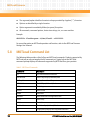
MOTLoad Command List . . . . . . . . . . . . . . . . . . . . . . . . . . . . . . . . . . . . . . . . . . . . . . . . . . . . . . . . . . . 100
Standard IPMI Commands . . . . . . . . . . . . . . . . . . . . . . . . . . . . . . . . . . . . . . . . . . . . . . . . . . . . . . . . . . 107
6.1.1 Global IPMI Commands . . . . . . . . . . . . . . . . . . . . . . . . . . . . . . . . . . . . . . . . . . . . . . . . . . . . . . 107
6.1.2 Watchdog Commands. . . . . . . . . . . . . . . . . . . . . . . . . . . . . . . . . . . . . . . . . . . . . . . . . . . . . . . 107
6.1.3 IPMI Messaging Commands . . . . . . . . . . . . . . . . . . . . . . . . . . . . . . . . . . . . . . . . . . . . . . . . . . 108
6.1.4 SEL Device Commands. . . . . . . . . . . . . . . . . . . . . . . . . . . . . . . . . . . . . . . . . . . . . . . . . . . . . . . 108
6.1.5 SDR Repository Commands . . . . . . . . . . . . . . . . . . . . . . . . . . . . . . . . . . . . . . . . . . . . . . . . . . 109
6.1.6 FRU Inventory Commands . . . . . . . . . . . . . . . . . . . . . . . . . . . . . . . . . . . . . . . . . . . . . . . . . . . 109
6.1.7 Sensor Device Commands. . . . . . . . . . . . . . . . . . . . . . . . . . . . . . . . . . . . . . . . . . . . . . . . . . . . 110
6.1.8 Chassis Device Commands . . . . . . . . . . . . . . . . . . . . . . . . . . . . . . . . . . . . . . . . . . . . . . . . . . . 111
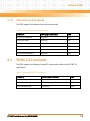
PICMG 2.9 Commands . . . . . . . . . . . . . . . . . . . . . . . . . . . . . . . . . . . . . . . . . . . . . . . . . . . . . . . . . . . . . 111
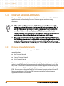
Emerson Specific Commands . . . . . . . . . . . . . . . . . . . . . . . . . . . . . . . . . . . . . . . . . . . . . . . . . . . . . . . 112
6.3.1 Firmware Upgrade Commands . . . . . . . . . . . . . . . . . . . . . . . . . . . . . . . . . . . . . . . . . . . . . . . 112
6.3.1.1 Start Firmware Upgrade . . . . . . . . . . . . . . . . . . . . . . . . . . . . . . . . . . . . . . . . . . . . 113
6.3.1.2 Continue Firmware Upgrade . . . . . . . . . . . . . . . . . . . . . . . . . . . . . . . . . . . . . . . . 114
6.3.1.3 Finish Firmware Upgrade . . . . . . . . . . . . . . . . . . . . . . . . . . . . . . . . . . . . . . . . . . . 114
6.3.2 OEM Commands . . . . . . . . . . . . . . . . . . . . . . . . . . . . . . . . . . . . . . . . . . . . . . . . . . . . . . . . . . . . 115
6.3.2.1 BMC/PM Change Role . . . . . . . . . . . . . . . . . . . . . . . . . . . . . . . . . . . . . . . . . . . . . . 116
6.3.2.2 Get Geographical Address . . . . . . . . . . . . . . . . . . . . . . . . . . . . . . . . . . . . . . . . . . 116
FRU Information . . . . . . . . . . . . . . . . . . . . . . . . . . . . . . . . . . . . . . . . . . . . . . . . . . . . . . . . . . . . . . . . . . 118
Sensor Description . . . . . . . . . . . . . . . . . . . . . . . . . . . . . . . . . . . . . . . . . . . . . . . . . . . . . . . . . . . . . . . . 118
CPCI-6200 Installation and Use (6806800J66C)
Contents
7
Memory Maps and Addresses . . . . . . . . . . . . . . . . . . . . . . . . . . . . . . . . . . . . . . . . . . . . . . . . . . . . . . . . . 137
7.1
7.2
7.3
7.4
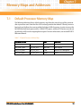
Default Processor Memory Map . . . . . . . . . . . . . . . . . . . . . . . . . . . . . . . . . . . . . . . . . . . . . . . . . . . . . 137
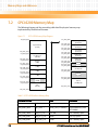
CPCI-6200 Memory Map . . . . . . . . . . . . . . . . . . . . . . . . . . . . . . . . . . . . . . . . . . . . . . . . . . . . . . . . . . . 138
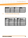
Local Bus Controller Memory Map . . . . . . . . . . . . . . . . . . . . . . . . . . . . . . . . . . . . . . . . . . . . . . . . . . . 139
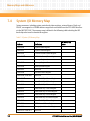
System I/O Memory Map . . . . . . . . . . . . . . . . . . . . . . . . . . . . . . . . . . . . . . . . . . . . . . . . . . . . . . . . . . . 140
7.4.1 System Status Register . . . . . . . . . . . . . . . . . . . . . . . . . . . . . . . . . . . . . . . . . . . . . . . . . . . . . . 143
7.4.2 System Control Register . . . . . . . . . . . . . . . . . . . . . . . . . . . . . . . . . . . . . . . . . . . . . . . . . . . . . 144
7.4.3 Front Panel LEDs Control and Status Register . . . . . . . . . . . . . . . . . . . . . . . . . . . . . . . . . . . 145
7.4.4 NOR Flash Control and Status Register . . . . . . . . . . . . . . . . . . . . . . . . . . . . . . . . . . . . . . . . . 146
7.4.5 Interrupt Register 1 . . . . . . . . . . . . . . . . . . . . . . . . . . . . . . . . . . . . . . . . . . . . . . . . . . . . . . . . . 148
7.4.6 Interrupt Register 2 . . . . . . . . . . . . . . . . . . . . . . . . . . . . . . . . . . . . . . . . . . . . . . . . . . . . . . . . . 149
7.4.7 Interrupt Mask Register . . . . . . . . . . . . . . . . . . . . . . . . . . . . . . . . . . . . . . . . . . . . . . . . . . . . . . 150
7.4.8 Presence Detect Register . . . . . . . . . . . . . . . . . . . . . . . . . . . . . . . . . . . . . . . . . . . . . . . . . . . . 151
7.4.9 NAND Flash Chip 1 Control Register . . . . . . . . . . . . . . . . . . . . . . . . . . . . . . . . . . . . . . . . . . . 153
7.4.10 NAND Flash Chip 1 Select Register . . . . . . . . . . . . . . . . . . . . . . . . . . . . . . . . . . . . . . . . . . . . 154
7.4.11 NAND Flash Chip 1 Presence Register . . . . . . . . . . . . . . . . . . . . . . . . . . . . . . . . . . . . . . . . . . 155
7.4.12 NAND Flash Chip 1 Status Register . . . . . . . . . . . . . . . . . . . . . . . . . . . . . . . . . . . . . . . . . . . . 156
7.4.13 NAND Flash Chip 2 Control Register . . . . . . . . . . . . . . . . . . . . . . . . . . . . . . . . . . . . . . . . . . . 157
7.4.14 NAND Flash Chip 2 Select Register . . . . . . . . . . . . . . . . . . . . . . . . . . . . . . . . . . . . . . . . . . . . 158
7.4.15 NAND Flash Chip 2 Presence Register . . . . . . . . . . . . . . . . . . . . . . . . . . . . . . . . . . . . . . . . . . 159
7.4.16 NAND Flash Chip 2 Status Register . . . . . . . . . . . . . . . . . . . . . . . . . . . . . . . . . . . . . . . . . . . . 160
7.4.17 CPCI Control and Status Register . . . . . . . . . . . . . . . . . . . . . . . . . . . . . . . . . . . . . . . . . . . . . . 161
7.4.18 Geographic Address Read Register . . . . . . . . . . . . . . . . . . . . . . . . . . . . . . . . . . . . . . . . . . . . 162
7.4.19 Watchdog Timer Load Register . . . . . . . . . . . . . . . . . . . . . . . . . . . . . . . . . . . . . . . . . . . . . . . 163
7.4.20 Watchdog Timer Control Register. . . . . . . . . . . . . . . . . . . . . . . . . . . . . . . . . . . . . . . . . . . . . 164
7.4.21 Watchdog Timer Resolution Register . . . . . . . . . . . . . . . . . . . . . . . . . . . . . . . . . . . . . . . . . . 165
7.4.22 Watchdog Timer Count Register . . . . . . . . . . . . . . . . . . . . . . . . . . . . . . . . . . . . . . . . . . . . . . 166
7.4.23 PLD Revision Register . . . . . . . . . . . . . . . . . . . . . . . . . . . . . . . . . . . . . . . . . . . . . . . . . . . . . . . . 167
7.4.24 PLD Date Code Register . . . . . . . . . . . . . . . . . . . . . . . . . . . . . . . . . . . . . . . . . . . . . . . . . . . . . . 168
7.4.25 Test Register 1 . . . . . . . . . . . . . . . . . . . . . . . . . . . . . . . . . . . . . . . . . . . . . . . . . . . . . . . . . . . . . . 168
7.4.26 Test Register 2 . . . . . . . . . . . . . . . . . . . . . . . . . . . . . . . . . . . . . . . . . . . . . . . . . . . . . . . . . . . . . . 169
7.4.27 External Timer Registers . . . . . . . . . . . . . . . . . . . . . . . . . . . . . . . . . . . . . . . . . . . . . . . . . . . . . 169
7.4.27.1 Prescaler Register . . . . . . . . . . . . . . . . . . . . . . . . . . . . . . . . . . . . . . . . . . . . . . . . . . 169
7.4.27.2 Control Registers . . . . . . . . . . . . . . . . . . . . . . . . . . . . . . . . . . . . . . . . . . . . . . . . . . 170
7.4.27.3 Compare Registers . . . . . . . . . . . . . . . . . . . . . . . . . . . . . . . . . . . . . . . . . . . . . . . . . 171
CPCI-6200 Installation and Use (6806800J66C)
7
Contents
Contents
7.5
7.6
7.7
A
Replacing the Battery . . . . . . . . . . . . . . . . . . . . . . . . . . . . . . . . . . . . . . . . . . . . . . . . . . . . . . . . . . . . . . . . 179
A.1
A.2
B
7.4.27.4 Counter Registers . . . . . . . . . . . . . . . . . . . . . . . . . . . . . . . . . . . . . . . . . . . . . . . . . . 172
Interrupt Controller . . . . . . . . . . . . . . . . . . . . . . . . . . . . . . . . . . . . . . . . . . . . . . . . . . . . . . . . . . . . . . . . 173
I2C Device Addresses . . . . . . . . . . . . . . . . . . . . . . . . . . . . . . . . . . . . . . . . . . . . . . . . . . . . . . . . . . . . . . 174
PCI/PCI-X Configuration . . . . . . . . . . . . . . . . . . . . . . . . . . . . . . . . . . . . . . . . . . . . . . . . . . . . . . . . . . . . 175
7.7.1 PCI IDSEL and Interrupt Assignment . . . . . . . . . . . . . . . . . . . . . . . . . . . . . . . . . . . . . . . . . . . 176
7.7.2 PCI Vendor and Device IDs . . . . . . . . . . . . . . . . . . . . . . . . . . . . . . . . . . . . . . . . . . . . . . . . . . . 176
7.7.3 PCI Arbitration Assignments . . . . . . . . . . . . . . . . . . . . . . . . . . . . . . . . . . . . . . . . . . . . . . . . . . 177
Battery Location . . . . . . . . . . . . . . . . . . . . . . . . . . . . . . . . . . . . . . . . . . . . . . . . . . . . . . . . . . . . . . . . . . . 179
Replacing the Battery . . . . . . . . . . . . . . . . . . . . . . . . . . . . . . . . . . . . . . . . . . . . . . . . . . . . . . . . . . . . . . 180
Related Documentation . . . . . . . . . . . . . . . . . . . . . . . . . . . . . . . . . . . . . . . . . . . . . . . . . . . . . . . . . . . . . . 181
B.1
B.2
B.3
Emerson Network Power - Embedded Computing Documents . . . . . . . . . . . . . . . . . . . . . . . . . . 181
Manufacturer’s Publications . . . . . . . . . . . . . . . . . . . . . . . . . . . . . . . . . . . . . . . . . . . . . . . . . . . . . . . . 182
Related Specifications . . . . . . . . . . . . . . . . . . . . . . . . . . . . . . . . . . . . . . . . . . . . . . . . . . . . . . . . . . . . . . 183
Safety Notes . . . . . . . . . . . . . . . . . . . . . . . . . . . . . . . . . . . . . . . . . . . . . . . . . . . . . . . . . . . . . . . . . . . . . . . . . . . . 185
Sicherheitshinweise . . . . . . . . . . . . . . . . . . . . . . . . . . . . . . . . . . . . . . . . . . . . . . . . . . . . . . . . . . . . . . . . . . . . . 189
Index . . . . . . . . . . . . . . . . . . . . . . . . . . . . . . . . . . . . . . . . . . . . . . . . . . . . . . . . . . . . . . . . . . . . . . . . . . . . . . . . . . 193
8
CPCI-6200 Installation and Use (6806800J66C)
List of Tables
Table 1-1
Table 1-2
Table 1-3
Table 2-1
Table 2-2
Table 2-3
Table 2-4
Table 3-1
Table 3-2
Table 3-3
Table 3-4
Table 3-5
Table 3-6
Table 3-7
Table 3-8
Table 3-9
Table 3-10
Table 3-11
Table 3-12
Table 3-13
Table 3-14
Table 3-15
Table 3-16
Table 3-17
Table 3-18
Table 3-19
Table 4-1
Table 4-2
Table 4-3
Table 4-4
Table 4-5
Table 4-6
Table 5-1
Table 6-1
Table 6-2
Table 6-3
Summary of Features . . . . . . . . . . . . . . . . . . . . . . . . . . . . . . . . . . . . . . . . . . . . . . . . . . . . . . . . 21
Order Numbers for Baseboard Variants . . . . . . . . . . . . . . . . . . . . . . . . . . . . . . . . . . . . . . . . 26
Order Numbers for Related Products . . . . . . . . . . . . . . . . . . . . . . . . . . . . . . . . . . . . . . . . . . 26
CPCI-6200 Environmental Requirements . . . . . . . . . . . . . . . . . . . . . . . . . . . . . . . . . . . . . . . 30
Baseboard Power Requirements . . . . . . . . . . . . . . . . . . . . . . . . . . . . . . . . . . . . . . . . . . . . . . 31
S1 Switch Settings . . . . . . . . . . . . . . . . . . . . . . . . . . . . . . . . . . . . . . . . . . . . . . . . . . . . . . . . . . 37
S2 Switch Settings . . . . . . . . . . . . . . . . . . . . . . . . . . . . . . . . . . . . . . . . . . . . . . . . . . . . . . . . . . 38
Onboard Connectors . . . . . . . . . . . . . . . . . . . . . . . . . . . . . . . . . . . . . . . . . . . . . . . . . . . . . . . . 47
CPCI Bus Connector Pinout, J1 . . . . . . . . . . . . . . . . . . . . . . . . . . . . . . . . . . . . . . . . . . . . . . . . 48
CPCI Bus Connector Pinout, J2 . . . . . . . . . . . . . . . . . . . . . . . . . . . . . . . . . . . . . . . . . . . . . . . . 49
CPCI User I/O Connector Pinout, J3 . . . . . . . . . . . . . . . . . . . . . . . . . . . . . . . . . . . . . . . . . . . . 50
CPCI User I/O Connector Pinout, J5 . . . . . . . . . . . . . . . . . . . . . . . . . . . . . . . . . . . . . . . . . . . . 52
PMC Connector Pinout, J11/J21 . . . . . . . . . . . . . . . . . . . . . . . . . . . . . . . . . . . . . . . . . . . . . . 53
PMC Connector Pinout, J12/J22 . . . . . . . . . . . . . . . . . . . . . . . . . . . . . . . . . . . . . . . . . . . . . . . 54
PMC Connector Pinout, J13/J23 . . . . . . . . . . . . . . . . . . . . . . . . . . . . . . . . . . . . . . . . . . . . . . 55
PMC Connector Pin Assignments , J14/J24 . . . . . . . . . . . . . . . . . . . . . . . . . . . . . . . . . . . . . 56
Front Panel Latch Pinout, P1 . . . . . . . . . . . . . . . . . . . . . . . . . . . . . . . . . . . . . . . . . . . . . . . . . . 59
DDR3 SO-DIMMs Pinout, XJ1 and XJ2 . . . . . . . . . . . . . . . . . . . . . . . . . . . . . . . . . . . . . . . . . . 60
PCI Express Expansion Connector Pinout, J17 . . . . . . . . . . . . . . . . . . . . . . . . . . . . . . . . . . . 62
IPMI Debug Pinout, P3 . . . . . . . . . . . . . . . . . . . . . . . . . . . . . . . . . . . . . . . . . . . . . . . . . . . . . . . 64
Processor Debug Header Pinout, P4 . . . . . . . . . . . . . . . . . . . . . . . . . . . . . . . . . . . . . . . . . . . 64
Boundary Scan Header Pinout, P5 . . . . . . . . . . . . . . . . . . . . . . . . . . . . . . . . . . . . . . . . . . . . . 65
COP Header Pinout, P6 . . . . . . . . . . . . . . . . . . . . . . . . . . . . . . . . . . . . . . . . . . . . . . . . . . . . . . 65
PCI Express Switch Header Pinout, P7 . . . . . . . . . . . . . . . . . . . . . . . . . . . . . . . . . . . . . . . . . . 66
Front Panel Reset Switch Pinout, P2 . . . . . . . . . . . . . . . . . . . . . . . . . . . . . . . . . . . . . . . . . . . 67
CPCI-6200 Status Indicators . . . . . . . . . . . . . . . . . . . . . . . . . . . . . . . . . . . . . . . . . . . . . . . . . . 68
PCI Buses 1 and 2 Frequency Requirements . . . . . . . . . . . . . . . . . . . . . . . . . . . . . . . . . . . . . 81
System Clock Frequencies . . . . . . . . . . . . . . . . . . . . . . . . . . . . . . . . . . . . . . . . . . . . . . . . . . . . 87
Reset Sources . . . . . . . . . . . . . . . . . . . . . . . . . . . . . . . . . . . . . . . . . . . . . . . . . . . . . . . . . . . . . . . 87
Reset Functions . . . . . . . . . . . . . . . . . . . . . . . . . . . . . . . . . . . . . . . . . . . . . . . . . . . . . . . . . . . . . 88
Reset Timing Requirements . . . . . . . . . . . . . . . . . . . . . . . . . . . . . . . . . . . . . . . . . . . . . . . . . . 90
Programming Devices . . . . . . . . . . . . . . . . . . . . . . . . . . . . . . . . . . . . . . . . . . . . . . . . . . . . . . . 93
MOTLoad Commands . . . . . . . . . . . . . . . . . . . . . . . . . . . . . . . . . . . . . . . . . . . . . . . . . . . . . . 100
Supported Global IPMI Commands . . . . . . . . . . . . . . . . . . . . . . . . . . . . . . . . . . . . . . . . . . . 107
Supported Watchdog Commands . . . . . . . . . . . . . . . . . . . . . . . . . . . . . . . . . . . . . . . . . . . . 107
Supported Watchdog Commands . . . . . . . . . . . . . . . . . . . . . . . . . . . . . . . . . . . . . . . . . . . . 108
CPCI-6200 Installation and Use (6806800J66C)
9
List of Tables
Table 6-4
Table 6-5
Table 6-6
Table 6-7
Table 6-8
Table 6-9
Table 6-10
Table 6-11
Table 6-12
Table 6-13
Table 6-14
Table 6-15
Table 6-16
Table 6-17
Table 6-18
Table 6-19
Table 6-20
Table 6-21
Table 6-22
Table 6-23
Table 6-24
Table 6-25
Table 6-26
Table 6-27
Table 6-28
Table 6-29
Table 6-30
Table 6-31
Table 6-32
Table 6-33
Table 6-34
Table 6-35
Table 6-36
Table 6-37
Table 6-38
Table 6-39
10
Supported SEL Device Commands . . . . . . . . . . . . . . . . . . . . . . . . . . . . . . . . . . . . . . . . . . . .108
Supported SDR Repository Commands . . . . . . . . . . . . . . . . . . . . . . . . . . . . . . . . . . . . . . . 109
Supported FRU Inventory Commands . . . . . . . . . . . . . . . . . . . . . . . . . . . . . . . . . . . . . . . . . 109
Supported Sensor Device Commands . . . . . . . . . . . . . . . . . . . . . . . . . . . . . . . . . . . . . . . . . 110
Supported Chassis Device Commands . . . . . . . . . . . . . . . . . . . . . . . . . . . . . . . . . . . . . . . . 111
Supported PICMG 2.9 Commands . . . . . . . . . . . . . . . . . . . . . . . . . . . . . . . . . . . . . . . . . . . .111
Firmware Upgrade Commands . . . . . . . . . . . . . . . . . . . . . . . . . . . . . . . . . . . . . . . . . . . . . . . 113
Response Data of Start Firmware Upgrade . . . . . . . . . . . . . . . . . . . . . . . . . . . . . . . . . . . . . 113
Request Data of Continue Firmware Upgrade . . . . . . . . . . . . . . . . . . . . . . . . . . . . . . . . . . 114
Response Data of Continue Firmware Upgrade . . . . . . . . . . . . . . . . . . . . . . . . . . . . . . . . . 114
Request Data of Finish Firmware Upgrade . . . . . . . . . . . . . . . . . . . . . . . . . . . . . . . . . . . . . 115
Response Data of Finish Firmware Upgrade . . . . . . . . . . . . . . . . . . . . . . . . . . . . . . . . . . . . 115
OEM Commands . . . . . . . . . . . . . . . . . . . . . . . . . . . . . . . . . . . . . . . . . . . . . . . . . . . . . . . . . . . 115
Request Data of BMC/PM Change Role . . . . . . . . . . . . . . . . . . . . . . . . . . . . . . . . . . . . . . . . 116
Response Data of BMC/PM Change Role . . . . . . . . . . . . . . . . . . . . . . . . . . . . . . . . . . . . . . . 116
Request Data of Get Geographical Address . . . . . . . . . . . . . . . . . . . . . . . . . . . . . . . . . . . . 117
Response Data of Get Geographical Address . . . . . . . . . . . . . . . . . . . . . . . . . . . . . . . . . . . 117
FRU Information CPCI-6200 . . . . . . . . . . . . . . . . . . . . . . . . . . . . . . . . . . . . . . . . . . . . . . . . . 118
IPMI Sensors Overview . . . . . . . . . . . . . . . . . . . . . . . . . . . . . . . . . . . . . . . . . . . . . . . . . . . . . . 118
Aggregate T Sensor . . . . . . . . . . . . . . . . . . . . . . . . . . . . . . . . . . . . . . . . . . . . . . . . . . . . . . . . . 120
Aggregate V Sensor . . . . . . . . . . . . . . . . . . . . . . . . . . . . . . . . . . . . . . . . . . . . . . . . . . . . . . . . 121
CPCI Signal Sensor . . . . . . . . . . . . . . . . . . . . . . . . . . . . . . . . . . . . . . . . . . . . . . . . . . . . . . . . . 121
CPU Status Sensor . . . . . . . . . . . . . . . . . . . . . . . . . . . . . . . . . . . . . . . . . . . . . . . . . . . . . . . . . . 122
Critical IRQ Sensor . . . . . . . . . . . . . . . . . . . . . . . . . . . . . . . . . . . . . . . . . . . . . . . . . . . . . . . . . . 123
Ejector Switch Sensor . . . . . . . . . . . . . . . . . . . . . . . . . . . . . . . . . . . . . . . . . . . . . . . . . . . . . . . 124
Max1617Temp Sensor . . . . . . . . . . . . . . . . . . . . . . . . . . . . . . . . . . . . . . . . . . . . . . . . . . . . . . 125
CoreTemp Sensor . . . . . . . . . . . . . . . . . . . . . . . . . . . . . . . . . . . . . . . . . . . . . . . . . . . . . . . . . . 126
SEL Fullness Sensor . . . . . . . . . . . . . . . . . . . . . . . . . . . . . . . . . . . . . . . . . . . . . . . . . . . . . . . . . 127
Signal Status Sensor . . . . . . . . . . . . . . . . . . . . . . . . . . . . . . . . . . . . . . . . . . . . . . . . . . . . . . . . 128
VCC1_2 Sensor . . . . . . . . . . . . . . . . . . . . . . . . . . . . . . . . . . . . . . . . . . . . . . . . . . . . . . . . . . . . 129
VCC1_5 Sensor . . . . . . . . . . . . . . . . . . . . . . . . . . . . . . . . . . . . . . . . . . . . . . . . . . . . . . . . . . . . 130
VCC1_8 Sensor . . . . . . . . . . . . . . . . . . . . . . . . . . . . . . . . . . . . . . . . . . . . . . . . . . . . . . . . . . . . 131
VCC3_3 Sensor . . . . . . . . . . . . . . . . . . . . . . . . . . . . . . . . . . . . . . . . . . . . . . . . . . . . . . . . . . . . 132
VCC2_5 Sensor . . . . . . . . . . . . . . . . . . . . . . . . . . . . . . . . . . . . . . . . . . . . . . . . . . . . . . . . . . . . 133
VCC5_0 Sensor . . . . . . . . . . . . . . . . . . . . . . . . . . . . . . . . . . . . . . . . . . . . . . . . . . . . . . . . . . . . 134
VCC1_0 Sensor . . . . . . . . . . . . . . . . . . . . . . . . . . . . . . . . . . . . . . . . . . . . . . . . . . . . . . . . . . . . 135
CPCI-6200 Installation and Use (6806800J66C)
List of Tables
Table 6-40
Table 7-1
Table 7-2
Table 7-3
Table 7-4
Table 7-5
Table 7-6
Table 7-7
Table 7-8
Table 7-9
Table 7-10
Table 7-11
Table 7-12
Table 7-13
Table 7-14
Table 7-15
Table 7-16
Table 7-17
Table 7-18
Table 7-19
Table 7-20
Table 7-21
Table 7-22
Table 7-23
Table 7-24
Table 7-25
Table 7-26
Table 7-27
Table 7-28
Table 7-29
Table 7-30
Table 7-31
Table 7-32
Table 7-33
Table 7-34
Table 7-35
VPCore Sensor . . . . . . . . . . . . . . . . . . . . . . . . . . . . . . . . . . . . . . . . . . . . . . . . . . . . . . . . . . . . . 136
Default Processor Address Map . . . . . . . . . . . . . . . . . . . . . . . . . . . . . . . . . . . . . . . . . . . . . . 137
CPCI-6200 Address Memory Map . . . . . . . . . . . . . . . . . . . . . . . . . . . . . . . . . . . . . . . . . . . . 138
LBC Memory Map and Chip Select Assignments . . . . . . . . . . . . . . . . . . . . . . . . . . . . . . . . 139
System I/O Memory Map . . . . . . . . . . . . . . . . . . . . . . . . . . . . . . . . . . . . . . . . . . . . . . . . . . . 140
System Status Register, 0xF200_0000 . . . . . . . . . . . . . . . . . . . . . . . . . . . . . . . . . . . . . . . . 143
System Status Register Field Definition . . . . . . . . . . . . . . . . . . . . . . . . . . . . . . . . . . . . . . . 143
System Control Register, 0xF200_0001 . . . . . . . . . . . . . . . . . . . . . . . . . . . . . . . . . . . . . . . 144
System Control Register Field Definition . . . . . . . . . . . . . . . . . . . . . . . . . . . . . . . . . . . . . . 145
Front Panel LED Control/Status Register, 0xF200_0002 . . . . . . . . . . . . . . . . . . . . . . . . . 145
Front Panel LED Control/Status Register Field Definition . . . . . . . . . . . . . . . . . . . . . . . . 146
NOR Flash Control/Status Register, 0xF200_0003 . . . . . . . . . . . . . . . . . . . . . . . . . . . . . . 146
NOR Flash Control/Status Register Field Definition . . . . . . . . . . . . . . . . . . . . . . . . . . . . . 146
Interrupt Register 1, 0xF200_0004 . . . . . . . . . . . . . . . . . . . . . . . . . . . . . . . . . . . . . . . . . . . 148
Interrupt Register 1 Field Definition . . . . . . . . . . . . . . . . . . . . . . . . . . . . . . . . . . . . . . . . . . 148
Interrupt Register 2, 0xF200_0005 . . . . . . . . . . . . . . . . . . . . . . . . . . . . . . . . . . . . . . . . . . . 149
Interrupt Register 2 Field Definition . . . . . . . . . . . . . . . . . . . . . . . . . . . . . . . . . . . . . . . . . . 149
Interrupt Mask Register, 0xF200_0006 . . . . . . . . . . . . . . . . . . . . . . . . . . . . . . . . . . . . . . . 150
Interrupt Mask Register . . . . . . . . . . . . . . . . . . . . . . . . . . . . . . . . . . . . . . . . . . . . . . . . . . . . . 150
Presence Detect Register, 0xF200_0008 . . . . . . . . . . . . . . . . . . . . . . . . . . . . . . . . . . . . . . 151
Presence Detect Register Field Definition . . . . . . . . . . . . . . . . . . . . . . . . . . . . . . . . . . . . . 152
NAND Flash Chip 1 Control Register, 0xF200_0010 . . . . . . . . . . . . . . . . . . . . . . . . . . . . . 153
NAND Flash Chip 1 Control Register Field Definition . . . . . . . . . . . . . . . . . . . . . . . . . . . . 153
NAND Flash Chip 1 Select Register, 0xF200_0011 . . . . . . . . . . . . . . . . . . . . . . . . . . . . . . 154
NAND Flash Chip 1 Select Register Field Definition . . . . . . . . . . . . . . . . . . . . . . . . . . . . . 154
NAND Flash Chip 1 Presence Register, 0xF200_0012 . . . . . . . . . . . . . . . . . . . . . . . . . . . 155
NAND Flash Chip 1 Presence Register Field Definition . . . . . . . . . . . . . . . . . . . . . . . . . . . 156
NAND Flash Chip 1 Status Register, 0xF200_0013 . . . . . . . . . . . . . . . . . . . . . . . . . . . . . . 156
NAND Flash Chip 1 Status Register Field Definition . . . . . . . . . . . . . . . . . . . . . . . . . . . . . 156
NAND Flash Chip 2 Control Register, 0xF200_0014 . . . . . . . . . . . . . . . . . . . . . . . . . . . . . 157
NAND Flash Chip 2 Control Register Field Definition . . . . . . . . . . . . . . . . . . . . . . . . . . . . 157
NAND Flash Chip 2 Select Register, 0xF200_0015 . . . . . . . . . . . . . . . . . . . . . . . . . . . . . . 158
NAND Flash Chip 2 Select Register . . . . . . . . . . . . . . . . . . . . . . . . . . . . . . . . . . . . . . . . . . . 158
NAND Flash Chip 2 Presence Register, 0xF200_0016 . . . . . . . . . . . . . . . . . . . . . . . . . . . 159
NAND Flash Chip 2 Presence Register Field Definition . . . . . . . . . . . . . . . . . . . . . . . . . . . 159
NAND Flash Chip 2 Status Register, 0xF200_0017 . . . . . . . . . . . . . . . . . . . . . . . . . . . . . . 160
CPCI-6200 Installation and Use (6806800J66C)
11
List of Tables
Table 7-36
Table 7-37
Table 7-38
Table 7-39
Table 7-40
Table 7-41
Table 7-42
Table 7-43
Table 7-44
Table 7-45
Table 7-46
Table 7-47
Table 7-48
Table 7-49
Table 7-50
Table 7-51
Table 7-52
Table 7-53
Table 7-54
Table 7-55
Table 7-56
Table 7-57
Table 7-58
Table 7-59
Table 7-60
Table 7-61
Table 7-62
Table B-1
Table B-2
Table B-3
12
NAND Flash Chip 2 Status Register Field Definition . . . . . . . . . . . . . . . . . . . . . . . . . . . . . 160
CPCI Control/Status Register, 0xF200_0018 . . . . . . . . . . . . . . . . . . . . . . . . . . . . . . . . . . . 161
CPCI Control/Status Register Field Definition . . . . . . . . . . . . . . . . . . . . . . . . . . . . . . . . . . 161
Geographic Address Read Register, 0xF200_0019 . . . . . . . . . . . . . . . . . . . . . . . . . . . . . . 162
Geographic Address Read Register Field Definition . . . . . . . . . . . . . . . . . . . . . . . . . . . . . 163
Watchdog Timer Load Register, 0xF200_0020 . . . . . . . . . . . . . . . . . . . . . . . . . . . . . . . . . 163
Watchdog Timer Control Register, 0xF200_0024 . . . . . . . . . . . . . . . . . . . . . . . . . . . . . . . 164
Watchdog Timer Control Register Field Definition . . . . . . . . . . . . . . . . . . . . . . . . . . . . . . 164
Watchdog Timer Resolution Register, 0xE200_0025 . . . . . . . . . . . . . . . . . . . . . . . . . . . . 165
Watchdog Timer Resolution Register . . . . . . . . . . . . . . . . . . . . . . . . . . . . . . . . . . . . . . . . . 165
Watchdog Timer Counter Register, 0xF200_0026 . . . . . . . . . . . . . . . . . . . . . . . . . . . . . . 166
PLD Revision Register, 0xF200_0030 . . . . . . . . . . . . . . . . . . . . . . . . . . . . . . . . . . . . . . . . . . 167
PLD Revision Register Field Definition . . . . . . . . . . . . . . . . . . . . . . . . . . . . . . . . . . . . . . . . . 167
PLD Date Code Register, 0xF200_0034 . . . . . . . . . . . . . . . . . . . . . . . . . . . . . . . . . . . . . . . . 168
PLD Date Code Register Field Definition . . . . . . . . . . . . . . . . . . . . . . . . . . . . . . . . . . . . . . . 168
Test Register 1, 0xF200_0038 . . . . . . . . . . . . . . . . . . . . . . . . . . . . . . . . . . . . . . . . . . . . . . . . 168
Test Register 2, 0xF200_003C . . . . . . . . . . . . . . . . . . . . . . . . . . . . . . . . . . . . . . . . . . . . . . . 169
Prescaler Register, 0xE202_0000 . . . . . . . . . . . . . . . . . . . . . . . . . . . . . . . . . . . . . . . . . . . . .169
Tick Timer Control Registers . . . . . . . . . . . . . . . . . . . . . . . . . . . . . . . . . . . . . . . . . . . . . . . . . 170
Tick Timer Control Field Definition . . . . . . . . . . . . . . . . . . . . . . . . . . . . . . . . . . . . . . . . . . . 170
Tick Timer Compare Registers . . . . . . . . . . . . . . . . . . . . . . . . . . . . . . . . . . . . . . . . . . . . . . . 171
Tick Timer Counter Register . . . . . . . . . . . . . . . . . . . . . . . . . . . . . . . . . . . . . . . . . . . . . . . . . 172
Interrupt Assignments . . . . . . . . . . . . . . . . . . . . . . . . . . . . . . . . . . . . . . . . . . . . . . . . . . . . . . 173
I2C Bus Device Addressing . . . . . . . . . . . . . . . . . . . . . . . . . . . . . . . . . . . . . . . . . . . . . . . . . . . 175
IDSEL and Interrupt Mapping for PCI Devices . . . . . . . . . . . . . . . . . . . . . . . . . . . . . . . . . . . 176
Planar PCI Device Identification . . . . . . . . . . . . . . . . . . . . . . . . . . . . . . . . . . . . . . . . . . . . . . 176
PCI Arbitration Assignments . . . . . . . . . . . . . . . . . . . . . . . . . . . . . . . . . . . . . . . . . . . . . . . . . 177
Related Publications . . . . . . . . . . . . . . . . . . . . . . . . . . . . . . . . . . . . . . . . . . . . . . . . . . . . . . . . 181
Manufacturers’ Publications . . . . . . . . . . . . . . . . . . . . . . . . . . . . . . . . . . . . . . . . . . . . . . . . . 182
Related Specifications . . . . . . . . . . . . . . . . . . . . . . . . . . . . . . . . . . . . . . . . . . . . . . . . . . . . . . 183
CPCI-6200 Installation and Use (6806800J66C)
List of Figures
Figure 1-1
Figure 1-2
Figure 2-1
Figure 3-1
Figure 3-2
Figure 3-3
Figure 4-1
Figure 4-2
Figure 4-3
Figure 4-4
Figure 4-5
Figure 4-6
Figure 4-7
Figure 4-8
Figure 4-9
Figure 7-1
Figure 7-2
Declaration of Conformity . . . . . . . . . . . . . . . . . . . . . . . . . . . . . . . . . . . . . . . . . . . . . . . . 25
Location of the Product Serial Number . . . . . . . . . . . . . . . . . . . . . . . . . . . . . . . . . . . . 27
Location of Configuration Switches . . . . . . . . . . . . . . . . . . . . . . . . . . . . . . . . . . . . . . . . 36
Board Layout . . . . . . . . . . . . . . . . . . . . . . . . . . . . . . . . . . . . . . . . . . . . . . . . . . . . . . . . . . . 45
USB Connector Pinout . . . . . . . . . . . . . . . . . . . . . . . . . . . . . . . . . . . . . . . . . . . . . . . . . . . 58
Serial Port Connector Pinout, J16 . . . . . . . . . . . . . . . . . . . . . . . . . . . . . . . . . . . . . . . . . . 59
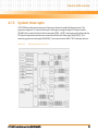
CPCI-6200 Block Diagram . . . . . . . . . . . . . . . . . . . . . . . . . . . . . . . . . . . . . . . . . . . . . . . . 72
Boot Block A . . . . . . . . . . . . . . . . . . . . . . . . . . . . . . . . . . . . . . . . . . . . . . . . . . . . . . . . . . . . 76
Boot Block B . . . . . . . . . . . . . . . . . . . . . . . . . . . . . . . . . . . . . . . . . . . . . . . . . . . . . . . . . . . . 77
PCI Express Bus Topology . . . . . . . . . . . . . . . . . . . . . . . . . . . . . . . . . . . . . . . . . . . . . . . . 79
System Controller Mode . . . . . . . . . . . . . . . . . . . . . . . . . . . . . . . . . . . . . . . . . . . . . . . . . 82
Peripheral Mode . . . . . . . . . . . . . . . . . . . . . . . . . . . . . . . . . . . . . . . . . . . . . . . . . . . . . . . . 83
Stand Alone Mode . . . . . . . . . . . . . . . . . . . . . . . . . . . . . . . . . . . . . . . . . . . . . . . . . . . . . . 84
Routing of Interrupt Sources . . . . . . . . . . . . . . . . . . . . . . . . . . . . . . . . . . . . . . . . . . . . . . 85
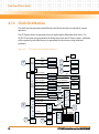
CPCI-6200 Clock Distribution Diagram . . . . . . . . . . . . . . . . . . . . . . . . . . . . . . . . . . . . 86
CPCI-6200 Memory Map Diagram . . . . . . . . . . . . . . . . . . . . . . . . . . . . . . . . . . . . . . . . 138
PCI Interrupt Mapping to Processor . . . . . . . . . . . . . . . . . . . . . . . . . . . . . . . . . . . . . . . 174
CPCI-6200 Installation and Use (6806800J66C)
13
List of Figures
14
CPCI-6200 Installation and Use (6806800J66C)
About this Manual
Overview of Contents
This manual is divided into the following chapters and appendices.
Introduction provides an overview of the features of the product, including ordering and
other product information like the location of labels.
Hardware Preparation and Installation discusses procedures on installing the CPCI
baseboard, PMC modules, and other accessories.
Controls, LEDs, and Connectors provides information on connector pinouts and board and
front panel layouts.
Functional Description discusses the main functional blocks on the product.
MOTLoad Firmwareprovides an overview and description of basic MOTLoad use including
implementation issues, a list of the initialization sequence, and a description of basic
commands.
Control via IPMI discusses the IPMI commands that the product supports.
Memory Maps and Addresses provides details on the various registers and addresses used in
the product.
Replacing the Battery provides instructions on how to replace the onboard battery.
Related Documentation provides a list of documentation relevant to the product.
Safety Notes lists the safety notes applicable to the product.
Sicherheitshinweise lists the German version of the safety notes.
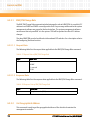
Abbreviations
This document uses the following abbreviations:
Abbreviation
Definition
ANSI
American National Standard Institute
BMC
Base Board Management Controller
CE
Chip Enable
COM
Communications
CPCI-6200 Installation and Use (6806800J66C)
15
About this Manual
About this Manual
16
Abbreviation
Definition
CPCI
Compact PCI
CPLD
Complex Programmable Logic Device
COP
Common On-Chip Processor
CRC
Cyclic Redundancy Check
DDR
Double Data Rate
DIMM
Dual Inline Memory Module
DMA
Direct Memory Access
DRAM
Dynamic Random Access Memory
DUART
Dual Universal Asynchronous Receiver/Transmitter
ECC
Error Correction Code
EEPROM
Electrically Erasable Programmable Read-Only Memory
EPROM
Erasable Programmable Read-Only Memory
ESD
Electrostatic Sensitive Device
ETSI
European Telecommunication Standards Institute
FCC
Federal Communications Commission
FRU
Field Replaceable Unit
GMII
Gigabit Media Independent Interface
GPCM
General Purpose Chip select Machine
IEEE
Institute of Electrical and Electronics Engineers
IPMB
Intelligent Platform Management Bus
IPMC
Intelligent Platform Management Interface Controller
IPMI
Intelligent Platform Management Interface
I2C
Inter Integrated Circuit
JTAG
Joint Test Access Group
LBC
Local Bus Controller
LFM
Linear Feet per Minute
LSB
Least Significant Byte
MPU
Multi Purpose Unit
CPCI-6200 Installation and Use (6806800J66C)
About this Manual
Abbreviation
Definition
MRAM
Magnetoresistive Random Access Memory
MSB
Most Significant Byte
Msb
Most Significant Bit
NEBS
Network Equipment Building System
NVRAM
Non-Volatile Random Access Memory
PCI
Peripheral Component Interconnect
PCIe or PCI-E
Peripheral Component Interconnect Express
PCI-X
Peripheral Component Interconnect -X
PHY
Physical Interface
PIC
Programmable Interrupt Controller
PIM
PCI Mezzanine Card Input/Output Module
PICMG
PCI Industrial Computer Manufacturers Group
PMC
PCI Mezzanine Card
PM
Peripheral Management
PLD
Programmable Logic Device
PLL
Phase-Locked Loop
PrPMC
Processor PCI Mezzanine Card
Rcv
Receive
RTC
Real-Time Clock
RTM
Rear Transition Module
SBC
Single Board Computer
SDR
Sensor Data Record
SDRAM
Synchronous Dynamic Random Access Memory
SEL
System Event Log
SMBus
System Management Bus
SMT
Surface Mount Technology
SO-DIMM
Small-Outline Dual In-line Memory Module
SO-UDIMM
Small-Outline Unbuffered Dual In-line Memory Module
CPCI-6200 Installation and Use (6806800J66C)
17
About this Manual
About this Manual
Abbreviation
Definition
SPD
Serial Presence Detect
SRAM
Static Random Access Memory
TSEC
Three-Speed Ethernet Controller
UART
Universal Asynchronous Receiver/Transmitter
VIO
Input/Output Voltage
VME
Versa Module Eurocard
VPD
Vital Product Data
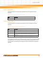
Conventions
The following table describes the conventions used throughout this manual.
18
Notation
Description
0x00000000
Typical notation for hexadecimal numbers (digits are
0 through F), for example used for addresses and
offsets
0b0000
Same for binary numbers (digits are 0 and 1)
bold
Used to emphasize a word
Screen
Used for on-screen output and code related elements
or commands in body text
Courier + Bold
Used to characterize user input and to separate it
from system output
Reference
Used for references and for table and figure
descriptions
File > Exit
Notation for selecting a submenu
<text>
Notation for variables and keys
[text]
Notation for software buttons to click on the screen
and parameter description
...
Repeated item for example node 1, node 2, ..., node
12
CPCI-6200 Installation and Use (6806800J66C)
About this Manual
Notation
Description
.
Omission of information from example/command
that is not necessary at the time being
.
.
..
Ranges, for example: 0..4 means one of the integers
0,1,2,3, and 4 (used in registers)
|
Logical OR
Indicates a hazardous situation which, if not avoided,
could result in death or serious injury
Indicates a hazardous situation which, if not avoided,
may result in minor or moderate injury
Indicates a property damage message
No danger encountered. Pay attention to important
information
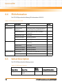
Summary of Changes
This manual has been revised and replaces all prior editions.
Part Number
Publication Date
Description
6806800J66C
August 2011
Updated Appendix P, Safety Notes, on page 185
6806800J66B
December 2010
Updated MOTLoad Command List on page 100
6806800J66A
September 2009
First edition
CPCI-6200 Installation and Use (6806800J66C)
19
About this Manual
About this Manual
20
CPCI-6200 Installation and Use (6806800J66C)
Chapter 1
Introduction
1.1
Features
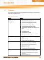
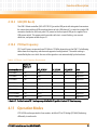
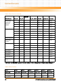
The CPCI-6200 is a high performance, hot swappable universal Compact PCI board based on
the MPC8572 integrated processor.
Table 1-1 Summary of Features
Function
Features
Processor
Host Controller
Memory Controller
One 8572 integrated processor
Two e500 cores with integrated 1 MB L2 cache
32 KB data and instruction cache on each core
Core frequency from 1.3 to 1.5 GHz
Two integrated DDR3 SDRAM controllers
Two integrated four-channel DMA controller
Two integrated PCI Express interfaces (8 lanes of 2.5 Gb/s
each)
Four integrated 10/100/1000 Ethernet controllers
One integrated DUART
Two integrated I2C controllers
One integrated programmable interrupt controller
One integrated local bus controller
Two banks of DDR3 SDRAM with error-correcting code
(ECC)
Supports 2 or 4 GB
Provides up to 800 MHz DDR3 data rate
One 8 KB VPD serial EEPROM
Two 64 KB user configuration serial EEPROMs
One real time clock (RTC) with battery back-up
Dual temperature sensors
Two SPDs for memory
Connection to the PCIE expander and RTM
128 MB soldered flash with two alternate 1 MB boot
sectors that can be selected via a hardware switch
HW switch or SW bit write protection for the entire
logical bank
Minimum of 4 GB user flash
System Memory
I2 C
Flash
CPCI-6200 Installation and Use (6806800J66C)
21
Introduction
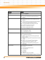
Table 1-1 Summary of Features (continued)
Function
Features
NVRAM
One 512 KB MRAM
PCI Express
4x port to PCI Express expansion
4x port to 6-port PCI Express switch for PCI Express
interface
One mini DB9 connector on the face plate (one serial
channel)
Two RJ-45 connectors on the face plate with integrated
LEDs for two 10/100/1000 Ethernet channels
Two 10/100/1000 Ethernet chanels for rear J3 I/O
One USB 2.0 channel on the face plate
PMC site 1 front I/O and rear J3 I/O
PMC site 2 front I/O and rear J5 I/O
Eight 32-bit MCP8572 timers
Four 32-bit timers in a PLD
One watchdog timer in PLD
I/O
Timers
CPCI Interface
IPMI Controller
22
Complies with the following:
PCI Specification Revision 2.2
PICMG 2.1 R2.0 CompactPCI Hot Swap Specification,
January 17, 2001
PICMG 2.0 R3.0 CompactPCI Core Specification, October
1, 1999
PICMG 2.16 R1.0 CompactPCI Packet Switching
Backplane Specification, September 5, 2001
PICMG 2.9 R1.0 CompactPCI System Management
Specification
Renesas HD65F2166 processor
Six I2C bus
8-channel analog/digital converter
Three serial ports
512 KB flash
40 KB SRAM
1 MB (64K x 16 bit) external SRAM
External user EEPROM, SDR/FRU, SEL flash of 512 KB each
CPCI-6200 Installation and Use (6806800J66C)
Introduction
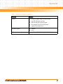
Table 1-1 Summary of Features (continued)
Function
Features
Others
One RESET/ABORT switch on the face plate
User/Fail LED on the face plate
Blue hot swap LED on the face plate
One standard 16-pin JTAG/COP header
Support for boundary scan
VxWorks
Linux
Software Support
RTM
CPCI-6200 Installation and Use (6806800J66C)
Compatible with RTM-CPCI-6115 (01-W3766F11A)
23
Introduction
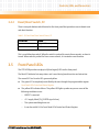
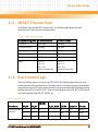
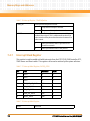
1.2
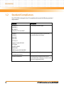
Standard Compliances
The CPCI-6200 is designed to be CE compliant and to meet the following standard
requirements.
Standard
Description
UL 60950-1
Safety Requirements (legal)
EN 60950-1
IEC 60950-1
CAN/CSA C22.2 No 60950-1
CISPR 22
CISPR 24
EMC requirements (legal) on system level
(predefined Emerson system)
EN 55022
EN 55024
FCC Part 15
Industry Canada ICES-003
VCCI Japan
AS/NZS CISPR 22
EN 300 386
NEBS Standard GR-1089 CORE
NEBS Standard GR-63-CORE
Environmental Requirements
ETSI EN 300 019 series
Directive 2002/95/EC
24
Directive on the restriction of the use of
certain hazardous substances in electrical and
electronic equipment (RoHS)
CPCI-6200 Installation and Use (6806800J66C)
Introduction
Figure 1-1
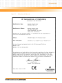
Declaration of Conformity
CPCI-6200 Installation and Use (6806800J66C)
25
Introduction
1.3
Mechanical Data
The CPCI-6200 is a full 6U 18-layer board. It is designed with ruggedization holes to support
ruggedization application. This board occupies a single CPCI card slot with PMC modules
installed.
1.4
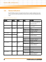
Ordering Information
Use the information in the following sections when ordering boards and accessories.
1.4.1
Supported Board Models
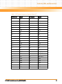
Table 1-2 Order Numbers for Baseboard Variants
1.4.2
Marketing Number
Description
CPCI6200-13-2G
MPC8572, 1.33 GHz, 2 GB SO-DIMM DDR3, 6E
CPCI6200-15-4G
MPC8572, 1.5 GHz, 4 GB SO-DIMM DDR3, 6E
Board Accessories
Table 1-3 Order Numbers for Related Products
Marketing Number
CPCI-6115-MCPTM-02
Description
Transition module/PIM carrier, two RJ-45 Ethernet connectors,
one RJ-45 asynchronous serial port connector, COM2 accessible
via PIM slots, two PIM slots.
26
CPCI-6200 Installation and Use (6806800J66C)
Introduction
1.5
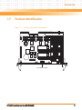
Product Identification
Figure 1-2
Location of the Product Serial Number
9105991
Serial Number Label
CPCI-6200 Installation and Use (6806800J66C)
27
Introduction
28
CPCI-6200 Installation and Use (6806800J66C)
Chapter 2
Hardware Preparation and Installation
2.1
Overview
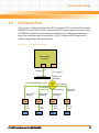
This chapter provides instructions on preparing and installing the CompactPCI board.
A fully implemented CPCI-6200 consists of the baseboard, PMC modules, and an optional rear
transition module.
2.2
Unpacking the CPCI Baseboard
1. Make sure that you receive all items of your shipment:
Printed Quick Start Guide and Safety Notes
CPCI-6200 baseboard
Optional items that were ordered
2. Check the board for damages, and report any damage to Emerson.
3. Remove the desiccant bag shipped together with the board and dispose of it
according to your country’s legislation.
The product is thoroughly inspected before shipment. If any damage occurred during
transportation or any items are missing, contact Emerson immediately.
CPCI-6200 Installation and Use (6806800J66C)
29
Hardware Preparation and Installation
2.3
Environmental Requirements
The environmental conditions must be tested and proven in the used system configuration.
These conditions refer to the surroundings of the board within the user environment.
Operating temperatures refer to the temperature of the air circulating around the board
and not to the component temperature.
To ensure that the operating conditions are met, forced air cooling is required within the
shelf environment.
The environmental values given in the table below only apply to the board without any
accessories. If installing accessories, their environmental requirements must also be
taken into account.
Product Damage
High humidity and condensation on surfaces cause short circuits.
Do not operate the product outside the specified environmental limits. Make sure the
product is completely dry and there is no moisture on any surface before applying power.
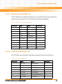
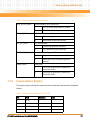
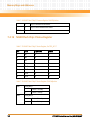
Table 2-1 CPCI-6200 Environmental Requirements
30
Characteristics
Operating
Non-Operating
Operating Temperature
0°C to +55°C (32°F to 131°F)
entry air with forced-air cooling
—40°C to +70°C (104°F to 158°F)
Temperature Change
+/-0.5°C/min according to NEBS
Standard GR-63-CORE
Forced Air Flow
8.7 LFM at 55°C (131 °F)
ambient temperature
Relative Humidity
5% to 90% Non-Condensed
5% to 90%Non-Condensed
Vibration
1.0 G sine sweep, 5—200 Hz,
0.25 octaves/min, all 3 axis
(operating)
5—20 Hz at 0.01 g/Hz
20—200 Hz at -3.0 dB/octave
Random 5—20 Hz at 1 m/sec
Random 20—200 Hz at -3 dB/Octave
CPCI-6200 Installation and Use (6806800J66C)
Hardware Preparation and Installation
Table 2-1 CPCI-6200 Environmental Requirements (continued)
Characteristics
Operating
Non-Operating
Shock
Half-sine, 11 ms, 30 ms
Blade-level packaging
Half-sine, 6 ms at 180 ms
Free Fall
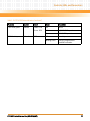
2.4
Blade-level packaging
100 mm (unpackaged) per GR-63CORE
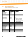
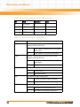
Power Requirements
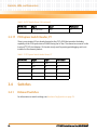
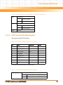
The board's power requirements depend on the installed hardware accessories. The following
table gives examples of typical power requirements for a processor running without any
accessories.
If you want to install any accessories, the load of the respective accessory has to be added to
the load of the board variant you are using. For information on the accessories' power
requirements, refer to the documentation delivered with the respective accessory or ask your
local representative.
Table 2-2 Baseboard Power Requirements
Configuration
Maximum Power Requirement
CPCI6200-13-2G (1.3 GHz, 2 GB memory)
3.3 V, 4.1 A, 13.5 W
5.0 V, 4.6 A, 23 W
CPCI6200-15-4G (1.5 GHz, 4 GB memory)
3.3 V, 4.2 A, 13.8 W
5.0 V, 5.7 A, 28.5 W (Estimated)
CPCI-6200 Installation and Use (6806800J66C)
31
Hardware Preparation and Installation
2.5
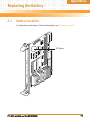
Installing Accessories
2.5.1
Installing a PMC Module on the CPCI Baseboard
One double-width or two single-width PCI mezzanine cards (PMC) can be mounted on the
CPCI-6200 baseboard. Each PMC slot has four connectors that provide a PCI interface to two
PMC slots that provide user I/O to the backplane.
Damage of Circuits
Electrostatic discharge and incorrect installation and removal of the product can damage
circuits or shorten their life.
Before touching the product make sure that your are working in an ESD-safe environment
or wear an ESD wrist strap or ESD shoes. Hold the product by its edges and do not touch any
components or circuits.
This procedure assumes that the CPCI-6200 is installed in the system chassis.
1. Attach an ESD strap to your wrist, and then attach the other end of the ESD strap to
the chassis as a ground.
The ESD strap must be secured to your wrist and to ground throughout the
procedure.
2. Remove chassis or system cover(s) as necessary for access to the board.
Personal Injury or Death
This product operates with dangerous voltages that can cause injury or death.
Use extreme caution when handling, testing, and adjusting this equipment and its
components.
3. Carefully remove the CPCI-6200 from the card slot and lay it flat, with connectors
J1 through J5 facing you.
32
CPCI-6200 Installation and Use (6806800J66C)
Hardware Preparation and Installation
4. Remove the PMC filler plate from the front panel of CPCI-6200.
PMC Alignment
PMC Filler Plate
Voltage Key
5. Make sure that hole on the PMC matches the voltage key on CPCI-6200.
Do not remove the PMC voltage key.
CPCI-6200 supports only 3.3 V I/O PMC modules.
6. Slide the edge connector of the PMC module into the front panel opening from
behind, and then place the PMC module on top of the baseboard.
CPCI-6200 Installation and Use (6806800J66C)
33
Hardware Preparation and Installation
The four connectors on the underside of the PMC module should then connect
smoothly with the corresponding connectors (J11/12/13/14) or (J21/22/23/24) on
CPCI-6200.
7. Insert the four short Phillips screws, provided with the PMC, through the holes on
the bottom side of CPCI-6200 and into the PMC front bezel and rear standoffs, and
then tighten the screws.
2.5.2
Installing the Rear Transition Module
For information on installing the rear transition module, see the "Transition Module
Preparation and Installation" chapter in the CPCI-6115 CompactPCI Single Board Computer
Installation and Use manual.
2.6
2.6.1
Preparing the Baseboard for Installation
Install the accessory kits, before installing the board, if necessary.
If memory modules have been installed, check that all socket locks of the board are
closed before board installation.
Inspecting the CPCI Baseboard
You can use the CPCI-6200 as a system controller in a system slot, an intelligent I/O board in a
peripheral slot, or in stand-alone mode.
The board is fully compliant to CompactPCI Hot Swap Specification PICMG 2.1 R2.0, and can
run in both 3.3 V and 5 V CompactPCI system.
Before installing the CPCI-6200, make sure that switches are configured as desired. For more
information, see Hardware Configuration on page 35.
34
CPCI-6200 Installation and Use (6806800J66C)
Hardware Preparation and Installation
Perform the following steps before you install your board into the CompactPCI backplane to
prevent possible backplane pin damage.
1. Inspect the board connectors to ensure that they are not damaged by previous
insertions or accidental mishandling.
If any connector is damaged, do not install the board into the backplane to prevent
the bending of pins.
2. Inspect the slot where the board will be installed for any bent pins on the backplane.
2.6.2
Equipment Required for Installation
You need the following items to do a complete installation:
2.6.3
CompactPCI or compatible system enclosure
System console terminal
Operating system and/or application software
Disk drives or other I/O, and controllers
Hardware Configuration
To produce the desired configuration and ensure proper operation of the board, you may need
to carry out certain hardware modifications before installing the module.
Most options on the board are configured by software. Configuration changes are made by
setting the bits in control registers after the board is installed in a system. The control registers
are described in Memory Maps and Addresses on page 137 and other vendor publications.
CPCI-6200 Installation and Use (6806800J66C)
35
Hardware Preparation and Installation
Switches are used to control options that are not software configurable. The switch settings are
described in the succeeding sections.
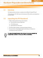
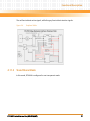
Figure 2-1
Location of Configuration Switches
Board
Configuration
Switch, S1
IPMI
Configuration
Switch, S2
2.6.3.1
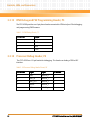
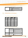
Board Configuration Switch, S1
The CPCI-6200 uses an 8-position SMT configuration switch to:
36
Control the flash bank write-protect.
Select the flash boot image.
Control the safe start ENV settings.
CPCI-6200 Installation and Use (6806800J66C)
Hardware Preparation and Installation
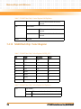
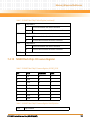
The default switch position is OFF.
Table 2-3 S1 Switch Settings
Switch
Name
ON
OFF (Default)
SW1
SAFE_START
Use safe ENV setting
Use normal ENV setting
SW2
BOOT_SEL
Board is booted from block
B of Flash A
Board is booted from block A
of Flash A
SW3
FLASH_WP
Flash A is write protected
Flash A write protection is off
SW4
JTAG_MODE
JTAG operates in pass
through mode
Normal operation
SW5
PMC1_PCI_FSEL
Max PCI freq can be
133 MHz on PMC1
Max PCI freq can be 100 MHz
on PMC1
SW6
SA_MODE
Board operates in Stand
Alone Mode
Normal operation
SW7
LRO_SW
Reset caused by front
panel switch, RTC, IPMI,
COP header is propagated
to backplane PCI reset
Reset caused by the front
panel switch, RTC, IPMI, COP
header is not propagated to
backplane PCI reset
SW8
PWR12V_EN
+-12 V supplies are
disabled
+-12 V supplies are enabled
When the SAFE_START switch is OFF, the normal ENV setting should be used. When it is on, the
safe ENV settings should be used. This switch status is readable from System Status register 1,
bit 5.
When the BOOT_SEL switch is OFF, the flash memory map is normal and boot block A is
selected. When the switch is ON, boot block B is selected and mapped to the highest address.
When the FLASH_WP switch is OFF, the flash is not write-protected. When it is ON, the flash is
write-protected i.e., writes to the flash devices are blocked by hardware.
When the JTAG_MODE switch is OFF, board operation is normal. When it is ON, the board is in
pass through mode.
When the PMC1_PCI_FSEL switch is OFF, the maximum PCI bus operation is 100 MHz on PMC1.
When it is ON, the maximum PCI bus operation is 100 MHz on PMC1. For more information,
see PCI Bus Frequency on page 81.
CPCI-6200 Installation and Use (6806800J66C)
37
Hardware Preparation and Installation
When the SA_MODE switch is OFF, board operation is normal. When the switch is ON, the
board operates in stand-alone mode i.e., it operates in a peripheral slot without the system
board in the chassis.
When the LRO_SW switch is OFF, if the board is placed in reset, it is only a local reset. When
the switch in ON, the board reset is propagated to CPCI bus. For more information, see Reset
Control Logic on page 87.
When the PWR12V_EN switch is OFF, the 12 V supply is enabled on the board and is available
for the RTM. When the switch is ON, the 12 V supply is disabled. Use the switch at ON position
when a 12 V supply is not available in the system or chassis.
2.6.3.2
IPMI Configuration Switch, S2
The CPCI-6200 uses an 8-position SMT configuration switch to control the IPMI controller
settings.
The default switch position is OFF.
Table 2-4 S2 Switch Settings
Switch
Name
ON
OFF (Default)
SW1
IPMI_DISABLE
Keep the IPMI controller in reset
and thereby disable it
IPMI controller is enabled
SW2
IPMI_MODE_2
JTAG Debug mode
Normal operation
SW3
IPMI_MODE_1
Reserved
Normal operation
SW4
-
Reserved
Reserved
SW5
IPMI_SYSEN
Force IPMI in system mode
IPMI operates in non-system
mode
SW6
FORCE_PM
Force IPMI in PM mode
IPMI operates in non-PM
mode
SW7
-
Reserved
Reserved
SW8
PMC2_PCI_FSEL
Max PCI freq can be 133 MHz on
PMC2
Max PCI freq can be 100 MHz
on PMC2
When the IPMI_DISABLE switch is OFF, the IPMI device is enabled. When the switch ON, IPMI is
disabled by asserting its reset.
38
CPCI-6200 Installation and Use (6806800J66C)
Hardware Preparation and Installation
When the IPMI_MODE_1 and IPMI_MODE_2 switches are OFF, the IPMI controller operates
normally. When both switches are ON, the IPMI controller enters programming mode. Any
other switch setting is not supported and treated as reserved.
When the IPMI_SYSEN switch is OFF, the IPMI operates in non-system mode. When the switch
is ON, IPMI operates in system mode.
When the FORCE_PM switch is OFF, the IPMI operates in non-peripheral management mode.
When the switch is ON, IPMI operates in peripheral management (PM) mode.
When the PMC2_PCI_FSEL switch is OFF, the maximum 100 MHz PCI bus frequency can be
used on PMC2 . When the switch is ON, the maximum PCI bus frequency is 133 MHz. For more
information, see PCI Bus Frequency on page 81.
2.7
Installing the CPCI Baseboard
1. Attach an ESD strap to your wrist, and then attach the other end of the ESD strap to
the chassis as a ground.
The ESD strap must be secured to your wrist and to ground throughout the
procedure.
2. For a non-hot swap system, shut down the operating system.
Personal Injury or Death
This product operates with dangerous voltages that can cause injury or death.
Use extreme caution when handling, testing, and adjusting this equipment and its
components.
3. Turn off the AC or DC power, and then remove the AC cord or DC power lines from
the system.
4. Remove the chassis or system cover(s) as necessary for access to the CompactPCI
modules.
CPCI-6200 Installation and Use (6806800J66C)
39
Hardware Preparation and Installation
5. Remove the filler panel from the appropriate card slot.
6. Set the VIO on the backplane to either +3.3 V or +5 V, depending on your
CompactPCI system signaling requirements, and ensure the backplane does not
bus J3 or J5 signals.
7. Slide the baseboard into the appropriate slot.
Grasping the top and bottom injector handles, be sure the module is well seated in
the P1 through P5 connectors on the backplane. Make sure you do not damage or
bend connector pins.
8. Secure the baseboard in the chassis with the screws provided, making good
contact with the transverse mounting rails to minimize RF emissions.
9. Replace the chassis or system cover(s), and make sure no cables are pinched.
10.Cable the peripherals to the panel connectors, and then reconnect the system to
the AC or DC power source.
11.Turn the equipment power on.
After you have verified that all necessary hardware preparation has been done, that all
connections have been made correctly and that the installation is complete, you can power up
the system. The MPU, hardware and firmware initialization process is performed by the
MOTLoad power-up or system reset. The firmware initializes the devices on the baseboard in
preparation for booting the operating system.
The firmware is shipped from the factory with an appropriate set of defaults. In most cases
there is no need to modify the firmware configuration before you boot the operating system.
For more information on MOTLoad, see MOTLoad Firmware on page 95.
40
CPCI-6200 Installation and Use (6806800J66C)
Hardware Preparation and Installation
2.8
Removing the CPCI Baseboard
The board is fully compliant to Compact PCI Hot Swap Specification PICMG 2.1 R2.0, and can
run in both 3.3 V and 5 V Compact PCI systems.
Data Loss
Removing the RTM with the system power on and the blue LED on the front blade still
flashing causes data loss.
Before removing the RTM from a powered system, power down the slot and the front
blade’s payload by opening the lower handle of the front blade and wait until the blue LED is
permanently ON.
Damage of Circuits
Electrostatic discharge and incorrect installation and removal of the product can damage
circuits or shorten their life.
Before touching the product make sure that your are working in an ESD-safe environment
or wear an ESD wrist strap or ESD shoes. Hold the product by its edges and do not touch any
components or circuits.
The following procedure describes how to remove the board from a system. It assumes that the
system is powered and running system level management software. If the system is
unpowered, disregard the blue LED and skip the respective step.
1. Unfasten the two screws on the front panel until the board is detached from the
rack frame.
2. Press the red button to unlock handles.
3. Open handles until resistance is encountered.
The hot swap switch opens automatically.
CPCI-6200 Installation and Use (6806800J66C)
41
Hardware Preparation and Installation
4. Wait until blue hot swap LED lights up.
Data Loss
Removing the product with the blue LED still blinking causes data loss.
Wait until the blue LED is permanently illuminated before removing the product.
5. Remove the board from the slot by fully opening the ejector handles.
2.9
Connecting to a Console Port
When the CPCI-6200 is installed in the chassis, you are ready to connect peripherals and apply
power to the board.
On the CPCI-6200 baseboard, the standard serial console port (COM1) serves as the MOTLoad
debugger console port. The firmware console should be set up as follows:
Eight bits per character
One stop bit per character
Parity disabled (no parity)
Baud rate of 9600
9600 baud is the power-up default for serial ports on CPCI-6200 boards. After power-up you
can reconfigure the baud rate if you wish, using the MOTLoad PF (Port Format) command via
the command line interface. Whatever the baud rate, some type of hardware
handshaking–either XON/OFF or via the RTS/CTS line–is desirable if the system supports it.
2.10
Factory-Installed Linux
A bootable ramdisk-based Linux image based on the 2.6.29.6 or later kernel is available in the
NOR flash. To boot this image, use the following MOTLoad commands:
CPCI6200> bmw -af8000000 -bf8ff0000 -c2000000
CPCI6200> execP -l2000400
42
CPCI-6200 Installation and Use (6806800J66C)
Hardware Preparation and Installation
The image should boot to the following prompt:
Emerson Network Power Embedded Computing Linux
Kernel 2.6.29.6 on a 2-processor CPCI6200
localhost login:
Login as root with no password.
If you want to use IPMI, load the IPMI SMBus driver using:
# modprobe ipmi_smb
Contact Emerson for kernel patches and additional information on using Linux on the CPCI6200.
CPCI-6200 Installation and Use (6806800J66C)
43
Hardware Preparation and Installation
44
CPCI-6200 Installation and Use (6806800J66C)
Chapter 3
Controls, LEDs, and Connectors
3.1
Board Layout
Figure 3-1
Board Layout
NAND Flash
J5
J3
J2
J1
Processor
PMC 1
PMC 2
PCI Express x4
to PCI Bridge 1,2,3
IPMI Controller
PCI Express
Switch
JTAG Header
DDR3 DIMM
LBC PLD
COP Header
PCI x1
to
PCI Bridge
Boot Flash
DDR3 DIMM
RTC
Battery
PCI Express Expansion
Configuration Configuration
Connector
Switch, S1
Switch, S2
USB Controller
CPCI-6200 Installation and Use (6806800J66C)
45
Controls, LEDs, and Connectors
3.2
Front Panel
For more information on the front panel connectors, see Front Panel LEDs on page 67.
Cutout for PMC Slot 2
covered with filler panel
Cutout for PMC Slot 1
covered with filler panel
Ethernet Port 1
Ethernet Port 2
USB Port
User/Fail LED (Green/Yellow)
Serial Port
Reset/Abort Switch
Hot Swap LED (Blue)
46
CPCI-6200 Installation and Use (6806800J66C)
Controls, LEDs, and Connectors
3.3
Connectors and Headers
Table 3-1 Onboard Connectors
Reference Designator
Function
J1
CPCI five-row J1
CPCI bus connector
J2
CPCI five-row J2
CPCI bus connector
J3
CPCI five-row J3
User I/O connector
J4
Not used
J5
CPCI five-row J5
User I/O connector
J6
10/100/1000 Ethernet
Ethernet port on the front panel (ENET 1 and ENET2)
J7
USB port on the front panel
J11, J12, J13, J14
PMC1
J21, J22, J23, J24
PMC2
J16
Serial Port 1 (COM1)
Mini DB9 serial port on the front panel
J17
PMC expansion to PMCspan
P1
Board insertion/ejection
Switch connector on the front panel
P2
Reset/abort switch on the front panel
P3
IPMI serial port (COM2)
Planar header for debugging IPMI Serial Port
P4
Processor debug header
Planar header for probing debug signals
P5
Boundary scan header
Planar header for boundary scan and PLD/flash programming
CPCI-6200 Installation and Use (6806800J66C)
47
Controls, LEDs, and Connectors
Table 3-1 Onboard Connectors (continued)
Reference Designator
Function
P6
Processor COP header
Planar header for processor COP emulation
P7
Planar header for debugging the PCI Express switch device
XJ1, XJ2
DDR3 DIMM 1 and 2 Socket
204-pin SO-UDIMM socket for DDR3 DIMM
3.3.1
S1
8-position switch
S2
8-position switch for IPMI functionality
CPCI Bus Connector, J1
J1 is a five-row CPCI bus connector.
Table 3-2 CPCI Bus Connector Pinout, J1
Pin
Row A
Row B
Row C
Row D
Row E
25
+5.0 V
REQ64#
ENUM#
+3.3 V
+5.0 V
24
AD[1]
+5.0 V
V(IO)1
AD[0]
ACK64#
23
+3.3 V
AD[4]
AD[3]
+5.0 V1
AD[2]
22
AD[7]
GND
+3.3 V1
AD[6]
AD[5]
21
+3.3 V
AD[9]
AD[8]
M66EN
C/BE[0]#
20
AD[12]
GND
V(IO)
AD[11]
AD[10]
19
+3.3 V
AD[15]
AD[14]
GND1
AD[13]
18
SERR#
GND
+3.3 V
PAR
C/BE[1]#
17
+3.3 V
IPMB0_SCL
IPMB0_SDA
GND1
PERR#
16
DEVSEL#
PCIXCAP
V(IO)
STOP#
LOCK#
15
+3.3 V
FRAME#
IRDY#
BD_SEL#
TRDY#
KEY AREA (Pins 12 - 14)
48
11
AD[18]
AD[17]
AD[16]
GND1
C/BE[2]#
10
AD[21]
GND
+3.3 V
AD[20]
AD[19]
CPCI-6200 Installation and Use (6806800J66C)
Controls, LEDs, and Connectors
Table 3-2 CPCI Bus Connector Pinout, J1 (continued)
3.3.2
Pin
Row A
Row B
Row C
Row D
Row E
9
C/BE[3]#
IDSEL
AD[23]
GND1
AD[22]
8
AD[26]
GND
V(IO)
AD[25]
AD[24]
7
AD[30]
AD[29]
AD[28]
GND1
AD[27]
6
REQ#
GND
+3.3 V1
CLK
AD[31]
5
BRSVR1A5
BRSVR1B5
RST#
GND1
GNT#
4
IPMB_PWR
HEALTHY#
V(IO)1
INTP
INTS
3
INTA#
INTB#
INTC#
+5.0 V1
INTD#
2
TCK
+5.0 V
TMS
TDO
TDI
1
+5.0 V
-12 V
TRST#
+12 V
+5.0 V
CPCI Bus Connector, J2
J2 is a five-row CPCI bus connector.
Table 3-3 CPCI Bus Connector Pinout, J2
Pin
Row A
Row B
Row C
Row D
Row E
22
GA4
GA3
GA2
GA1
GA0
21
RSV
GND
RSV
RSV
RSV
20
RSV
GND
RSV
GND
RSV
19
GND
GND
RSV
RSV
RSV
18
BRSVP2A18
BRSVP2B18
BRSVP2C18
GND
BRSVP2E18
17
BRSVP2A17
GND
RSV
RSV
RSV
16
BRSVP2A16
BRSVP2B16
RSV
GND
BRSVP2E16
15
BRSVP2A15
GND
RSV
RSV
RSV
14
AD[35]
AD[34]
AD[33]
GND
AD[32]
13
AD[38]
GND
V(IO)
AD[37]
AD[36]
12
AD[42]
AD[41]
AD[40]
GND
AD[39]
11
AD[45]
GND
V(IO)
AD[44]
AD[43]
CPCI-6200 Installation and Use (6806800J66C)
49
Controls, LEDs, and Connectors
Table 3-3 CPCI Bus Connector Pinout, J2 (continued)
Pin
Row A
Row B
Row C
Row D
Row E
10
AD[49]
AD[48]
AD[47]
GND
AD[46]
9
AD[52]
GND
V(IO)
AD[51]
AD[50]
8
AD[56]
AD[55]
AD[54]
GND
AD[53]
7
AD[59]
GND
V(IO)
AD[58]
AD[57]
6
AD[63]
AD[62]
AD[61]
GND
AD[60]
5
C/BE[5]#
64EN#
V(IO)
C/BE[4]#
PAR64
4
V(IO)
BRSVP2B4
C/BE[7]#
GND
C/BE[6]#
3
RSV
GND
RSV
RSV
RSV
1
2
RSV
RSV
SYSEN#
RSV
RSV
1
RSV
GND
RSV
RSV
RSV
1. Defined as SYSEN#. This OV allows the CPCI-6200 to ensure that it is installed into a peripheral slot.
3.3.3
CPCI User I/O Connector, J3
J3 is a five-row user I/O CPCI connector.
Note: Row F is ground and is not shown in the table.
Table 3-4 CPCI User I/O Connector Pinout, J3
50
Pin
Row A
Row B
Row C
Row D
Row E
1
IPMI_PWR
PMCIO64
PMCIO63
PMCIO62
PMCIO61
2
PMCIO60
PMCIO59
PMCIO58
PMCIO57
PMCIO56
3
PMCIO55
PMCIO54
PMCIO53
PMCIO52
PMCIO51
4
PMCIO50
PMCIO49
PMCIO48
PMCIO47
PMCIO46
5
PMCIO45
PMCIO44
PMCIO43
PMCIO42
PMCIO41
6
PMCIO40
PMCIO39
PMCIO38
PMCIO37
PMCIO36
7
PMCIO35
PMCIO34
PMCIO33
PMCIO32
PMCIO31
8
PMCIO30
PMCIO29
PMCIO28
PMCIO27
PMCIO26
CPCI-6200 Installation and Use (6806800J66C)
Controls, LEDs, and Connectors
Table 3-4 CPCI User I/O Connector Pinout, J3 (continued)
Pin
Row A
Row B
Row C
Row D
Row E
9
PMCIO25
PMCIO24
PMCIO23
PMCIO22
PMCIO21
10
PMCIO20
PMCIO19
PMCIO18
PMCIO17
PMCIO16
11
PMCIO15
PMCIO14
PMCIO13
PMCIO12
PMCIO11
12
PMCIO10
PMCIO9
PMCIO8
PMCIO7
PMCIO6
13
PMCIO5
PMCIO4
PMCIO3
PMCIO2
PMCIO1
14
+3.3V
+3.3V
+3.3V
+5V
+5V
15
G1_DB+ (RX2+)
G1_DB- (RX2-)
GND
G1_DD+
G1_DD-
16
G1_DA+ (TX2+)
G1_DA- (TX2-)
GND
G1_DC+
G1_DC-
17
G0_DB+ (RX1+)
G0_DB- (RX1-)
GND
G0_DD+
G0_DD-
18
G0_DA+ (TX1+)
G0_DA- (TX1-)
GND
G0_DC+
G0_DC-
19
GND
+12V
-12V
GND
GND
10/100/1000Base-T Ethernet signals:
G0_Dx—CH1 10/100/1000Base-T Ethernet
G1_Dx—CH2 10/100/1000Base-T Ethernet
PMC User I/O signals:
3.3.4
PMCIO(64:1)—PMC I/O
IPMI_PWR—+3.3 V derived from IPMB input power
CPCI Connector, J4
J4 is a five-row CPCI connector that is not used on the CPCI-6200. It is not populated.
3.3.5
CPCI User I/O Connector, J5
J5 is a five-row user I/O CPCI connector.
CPCI-6200 Installation and Use (6806800J66C)
51
Controls, LEDs, and Connectors
Row F is ground and is not shown in the table.
Table 3-5 CPCI User I/O Connector Pinout, J5
3.3.6
Pin
Row A
Row B
Row C
Row D
Row E
1
TM_PRSNT#
PMCIO64
PMCIO63
PMCIO62
PMCIO61
2
PMCIO60
PMCIO59
PMCIO58
PMCIO57
PMCIO56
3
PMCIO55
PMCIO54
PMCIO53
PMCIO52
PMCIO51
4
PMCIO50
PMCIO49
PMCIO48
PMCIO47
PMCIO46
5
PMCIO45
PMCIO44
PMCIO43
PMCIO42
PMCIO41
6
PMCIO40
PMCIO39
PMCIO38
PMCIO37
PMCIO36
7
PMCIO35
PMCIO34
PMCIO33
PMCIO32
PMCIO31
8
PMCIO30
PMCIO29
PMCIO28
PMCIO27
PMCIO26
9
PMCIO25
PMCIO24
PMCIO23
PMCIO22
PMCIO21
10
PMCIO20
PMCIO19
PMCIO18
PMCIO17
PMCIO16
11
PMCIO15
PMCIO14
PMCIO13
PMCIO12
PMCIO11
12
PMCIO10
PMCIO9
PMCIO8
PMCIO7
PMCIO6
13
PMCIO5
PMCIO4
PMCIO3
PMCIO2
PMCIO1
14
NC
NC
NC
NC
NC
15
NC
NC
GND
NC
NC
16
NC
NC
NC
NC
NC
17
GND
NC
NC
NC
NC
18
NC
NC
TMCOM3#
I2C_CLK
I2C_DATA
19
NC
NC
NC
MXCLK
MXSYNC#
20
NC
NC
NC
MXDI
MXDO
21
NC
NC
NC
COM4_RXD
COM3_RXD
22
NC
NC
NC
COM4_TXD
COM4_TXD
PCI Mezzanine Card (PMC) Connectors
There are four 64-pin connectors for each PMC slot on the CPCI-6200.
52
CPCI-6200 Installation and Use (6806800J66C)
Controls, LEDs, and Connectors
Connectors J11, J12, J13 and J14 are used for PMC1 while J21, J22, J23 and J24 are used for
PMC2.
Table 3-6 PMC Connector Pinout, J11/J21
Pin
J11/J21
Pin
1
TCK
-12 V
2
3
GND
INTA#
4
5
INTB#
INTC#
6
7
PRESENT#
+5 V
8
9
INTD#
PCI_RSVD
10
11
GND
NC (+3.3Vaux)
12
13
CLK
GND
14
15
GND
GNT#/XREQ0#
16
17
REQ#/XGNT0#
+5 V
18
19
VIO
AD31
20
21
AD28
AD27
22
23
AD25
GND
24
25
GND
C/BE3#
26
27
AD22
AD21
28
29
AD19
+5 V
30
31
VIO
AD17
32
33
FRAME#
GND
34
35
GND
IRDY#
36
37
DEVSEL#
+5 V
38
39
PCIXCAP
LOCK#
40
41
PCI_RSVD
PCI_RSVD
42
43
PAR
GND
44
45
VIO
AD15
46
47
AD12
AD11
48
49
AD09
+5 V
50
CPCI-6200 Installation and Use (6806800J66C)
53
Controls, LEDs, and Connectors
Table 3-6 PMC Connector Pinout, J11/J21 (continued)
Pin
J11/J21
Pin
51
GND
C/BE0#
52
53
AD06
AD05
54
55
AD04
GND
56
57
VIO
AD03
58
59
AD02
AD01
60
61
AD00
+5 V
62
63
GND
REQ64#
64
Table 3-7 PMC Connector Pinout, J12/J22
54
Pin
J12
J22
Pin
1
+12 V
TRST#
2
3
TMS
TDO
4
5
TDI
GND
6
7
GND
PCI_RSVD
8
9
PCI_RSVD
PCI_RSVD
10
11
MOT_RSVD
+3.3 V
12
13
RST#
MOT_RSVD
14
15
+3.3 V
MOT_RSVD
16
17
NC (PME#)
GND
18
19
AD30
AD29
20
21
GND
AD26
22
23
AD24
+3.3 V
24
25
IDSEL
AD23
26
27
+3.3 V
AD20
28
29
AD18
GND
30
31
AD16
C/BE2#
32
33
GND
IDSELB
34
CPCI-6200 Installation and Use (6806800J66C)
Controls, LEDs, and Connectors
Table 3-7 PMC Connector Pinout, J12/J22 (continued)
Pin
J12
J22
Pin
35
TRDY#
+3.3 V
36
37
GND
STOP#
38
39
PERR#
GND
40
41
+3.3 V
SERR#
42
43
C/BE1#
GND
44
45
AD14
AD13
46
47
M66EN
AD10
48
49
AD08
+3.3 V
50
51
AD07
REQB_L
52
53
+3.3 V
GNTB_L
54
55
MOT_RSVD
GND
56
57
MOT_RSVD
EREADY
58
59
GND
NC (RESETOUT_L)
60
61
ACK64#
+3.3 V
62
63
GND
NC (MONARCH#)
64
Table 3-8 PMC Connector Pinout, J13/J23
Pin
J13/J23
Pin
1
PCI_RSVD
GND
2
3
GND
C/BE7#
4
5
C/BE6#
C/BE5#
6
7
C/BE4# (Note 1)
GND
8
9
VIO
PAR64
10
11
AD63
AD62
12
13
AD61
GND
14
15
GND
AD60
16
17
AD59
AD58
18
CPCI-6200 Installation and Use (6806800J66C)
55
Controls, LEDs, and Connectors
Table 3-8 PMC Connector Pinout, J13/J23 (continued)
Pin
J13/J23
Pin
19
AD57
GND
20
21
VIO
AD56
22
23
AD55
AD54
24
25
AD53
GND
26
27
GND
AD52
28
29
AD51
AD50
30
31
AD49
GND
32
33
GND
AD48
34
35
AD47
AD46
36
37
AD45
GND
38
39
VIO
AD44
40
41
AD43
AD42
42
43
AD41
GND
44
45
GND
AD40
46
47
AD39
AD38
48
49
AD37
GND
50
51
GND
AD36
52
53
AD35
AD34
54
55
AD33
GND
56
57
VIO
AD32
58
59
PCI_RSVD
PCI_RSVD
60
61
PCI_RSVD
GND
62
63
GND
PCI_RSVD
64
Table 3-9 PMC Connector Pin Assignments , J14/J24
Pin
1
56
J14/J24
PMCIO1
PMCIO2
Pin
2
CPCI-6200 Installation and Use (6806800J66C)
Controls, LEDs, and Connectors
Table 3-9 PMC Connector Pin Assignments , J14/J24 (continued)
Pin
J14/J24
Pin
3
PMCIO3
PMCIO4
4
5
PMCIO5
PMCIO6
6
7
PMCIO7
PMCIO8
8
9
PMCIO9
PMCIO10
10
11
PMCIO11
PMCIO12
12
13
PMCIO13
PMCIO14
14
15
PMCIO15
PMCIO16
16
17
PMCIO17
PMCIO18
18
19
PMCIO19
PMCIO20
20
21
PMCIO21
PMCIO22
22
23
PMCIO23
PMCIO24
24
25
PMCIO25
PMCIO26
26
27
PMCIO27
PMCIO28
28
29
PMCIO29
PMCIO30
30
31
PMCIO31
PMCIO32
32
33
PMCIO33
PMCIO34
34
35
PMCIO35
PMCIO36
36
37
PMCIO37
PMCIO38
38
39
PMCIO39
PMCIO40
40
41
PMCIO41
PMCIO42
42
43
PMCIO43
PMCIO44
44
45
PMCIO45
PMCIO46
46
47
PMCIO47
PMCIO48
48
49
PMCIO49
PMCIO50
50
51
PMCIO51
PMCIO52
52
53
PMCIO53
PMCIO54
54
55
PMCIO55
PMCIO56
56
CPCI-6200 Installation and Use (6806800J66C)
57
Controls, LEDs, and Connectors
Table 3-9 PMC Connector Pin Assignments , J14/J24 (continued)
Pin
3.3.7
J14/J24
Pin
57
PMCIO57
PMCIO58
58
59
PMCIO59
PMCIO60
60
61
PMCIO61
PMCIO62
62
63
PMCIO63
PMCIO64
64
Ethernet Connector
There are two Ethernet ports on the front panel through a single connector J6.
J6 is a single housing with two RJ-45 ports. The pin configuration is based on IEEE standards
802.3ab-1999.
3.3.8
USB Connector
There is one standard 4-pin USB connector located on the front panel.
Figure 3-2
USB Connector Pinout
1 5V
2 USB_DATA +
3 USB_DATA GND
58
1
4
CPCI-6200 Installation and Use (6806800J66C)
Controls, LEDs, and Connectors
3.3.9
Serial Port Connector, J16
The serial port connector (COM1) is located on the front panel.
Figure 3-3
1
2
3
4
5
Serial Port Connector Pinout, J16
Not Connected
RXD
TXD
Not Connected
GND
1
6 Not Connected
9
5
RTS#
CTS#
Not Connected
6
7
8
9
Note: G1 and G2 are connected to ground.
3.3.10 Board Insertion/Extraction Connector, P1
A board insertion and extraction connector is located near the front panel. This connector is
used to detect a board insertion or extraction event. The latch connector on the front panel is
connected to this connector.
Table 3-10 Front Panel Latch Pinout, P1
Pin Number
Signal
1
GND
2
BOARD_EJECT
3
FP_EJECTSW
G1
NC
G2
NC
Pins 1 and 2 indicate board insertion or extraction status. Pin 2 is used with the PCI Bridge while
pin 3 is used with the IPMI controller.
A closed latch indicates board insertion. In this case, pin 2 and 3 are shorted and
FP_EJECTSW = 1, BOARD_EJECT = 0.
CPCI-6200 Installation and Use (6806800J66C)
59
Controls, LEDs, and Connectors
3.3.11 DDR3 SO-DIMM Connectors, XJ1 and XJ2
The CPCI-6200 provides two 204-pin DDR3 SO-UDIMM connectors for installing DDR3
SDRAMs.
Table 3-11 DDR3 SO-DIMMs Pinout, XJ1 and XJ2
Pin Number
Signal
Pin Number
Signal
Pin Number
Signal
Pin Number
Signal
1
VREFDQ
2
VSS
103
A3
104
A4
3
VSS
4
DQ4
105
A1
106
A2
5
DQ0
6
DQ5
107
A0
108
BA1
7
DQ1
8
VSS
109
VDD
110
VDD
9
VSS
10
DQS0#
111
CK0
112
PAR_IN/CK1
11
DM0
12
DQS0
113
CK0#
114
ERR_OUT/CK1#
13
DQ2
14
VSS
115
VDD
116
VDD
15
DQ3
16
DQ6
117
A10/AP
118
CS3#
17
VSS
18
DQ7
119
BA0
120
CS2#
19
DQ8
20
VSS
121
WE#
122
RAS#
21
DQ9
22
DQ12
123
VDD
124
VDD
23
VSS
24
DQ13
125
CAS#
126
ODT0
25
DQS1#
26
VSS
127
CS0#
128
ODT1
27
DQS1
28
DM1
129
CS1#
130
A13
29
VSS
30
RESET#
131
VDD
132
VDD
31
DQ10
32
VSS
133
DQ32
134
DQ36
33
DQ11
34
DQ14
135
DQ33
136
DQ37
35
VSS
36
DQ15
137
VSS
138
VSS
37
DQ16
38
VSS
139
DQS4#
140
DM4
39
DQ17
40
DQ20
141
DQS4
142
DQ38
41
VSS
42
DQ21
143
VSS
144
DQ39
43
DQS2#
44
DM2
145
DQ34
146
VSS
45
DQS2
46
VSS
147
DQ35
148
DQ44
60
CPCI-6200 Installation and Use (6806800J66C)
Controls, LEDs, and Connectors
Table 3-11 DDR3 SO-DIMMs Pinout, XJ1 and XJ2 (continued)
Pin Number
Signal
Pin Number
Signal
Pin Number
Signal
Pin Number
Signal
47
VSS
48
DQ22
149
VSS
150
DQ45
49
DQ18
50
DQ23
151
DQ40
152
VSS
51
DQ19
52
VSS
153
DQ41
154
DQS5#
53
VSS
54
DQ28
155
VSS
156
DQS5
55
DQ24
56
DQ29
157
DM5
158
VSS
57
DQ25
58
VSS
159
DQ42
160
DQ46
59
DM3
60
DQS3#
161
DQ43
162
DQ47
61
VSS
62
DQS3
163
VSS
164
VSS
63
DQ26
64
VSS
165
DQ48
166
DQ52
65
DQ27
66
DQ30
167
DQ49
168
DQ53
67
VSS
68
DQ31
169
VSS
170
VSS
69
CB0
70
VSS
171
DQS6#
172
DM6
71
CB1
72
CB4
173
DQS6
174
DQ54
73
VSS
74
CB5
175
VSS
176
DQ55
75
DQS8#
76
DM8
177
DQ50
178
VSS
77
DQS8
78
VSS
179
DQ51
180
DQ60
79
VSS
80
CB6
181
VSS
182
DQ61
81
CB2
82
CB7
183
DQ56
184
VSS
83
CB3
84
VREFCA
185
DQ57
186
DQS7#
85
VDD
86
VDD
187
VSS
188
DQS7
87
CKE0
88
A15
189
DM7
190
VSS
89
CKE1
90
A14
191
DQ58
192
DQ62
91
BA2
92
A9
193
DQ59
194
DQ63
93
VDD
94
VDD
195
VSS
196
VSS
95
A12/BC#
96
A11
197
SA0
198
EVENT#
97
A8
98
A7
199
VDDSPD
200
SDA
99
A5
100
A6
201
SA1
202
SCL
CPCI-6200 Installation and Use (6806800J66C)
61
Controls, LEDs, and Connectors
Table 3-11 DDR3 SO-DIMMs Pinout, XJ1 and XJ2 (continued)
Pin Number
Signal
Pin Number
Signal
Pin Number
Signal
Pin Number
Signal
101
VDD
102
VDD
203
VTT
204
VTT
3.3.12 PCI Express Expansion Connector, J17
The CPCI-6200 provides PCI Express expansion capability through 76-pin Mictor connector.
Table 3-12 PCI Express Expansion Connector Pinout, J17
62
Pin Number
Signal
Pin Number
Signal
1
GND
2
GND
3
TX0_P
4
RX0_P
5
TX0_N
6
RX0_N
7
GND
8
GND
9
TX1_P
10
RX1_P
11
TX1_N
12
RX1_N
13
GND
14
GND
15
TX2_P
16
RX2_P
17
TX2_N
18
RX2_N
19
GND
20
GND
21
TX3_P
22
RX3_P
23
TX3_N
24
RX3_N
25
GND
26
GND
27
CLK_P
28
NC
29
CLK_N
30
NC
31
GND
32
GND
33
NC
34
NC
35
NC
36
END#
37
INT#
38
RESET#
39
GND
40
GND
CPCI-6200 Installation and Use (6806800J66C)
Controls, LEDs, and Connectors
Table 3-12 PCI Express Expansion Connector Pinout, J17
Pin Number
Signal
Pin Number
Signal
41
NC
42
NC
43
NC
44
NC
45
GND
46
GND
47
NC
48
NC
49
NC
50
NC
51
GND
52
GND
53
NC
54
NC
55
NC
56
NC
57
GND
58
GND
59
NC
60
NC
61
NC
62
NC
63
GND
64
GND
65
NC
66
NC
67
NC
68
NC
69
TDI
70
TDO
71
TRST#
72
I2C_CLK
73
TMS
74
I2C_DATA
75
TCK
76
PRESENT#
G1
GND
G2
GND
G3
GND
G4
GND
G5
GND
G6
GND
G7
GND
G8
GND
G9
GND
G10
GND
CPCI-6200 Installation and Use (6806800J66C)
63
Controls, LEDs, and Connectors
3.3.13 IPMI Debug and FW Programming Header, P3
The CPCI-6200 provides one 4-pin planar header connected to IPMI serial port 2 for debugging
and programming IPMI firmware.
Table 3-13 IPMI Debug Pinout, P3
Pin Number
Signal
1
TXD
2
GND
3
RXD
4
GND
3.3.14 Processor Debug Header, P4
The CPCI-6200 has a 10-pin header for debugging. This header can debug a DDR or LBC
interface.
Table 3-14 Processor Debug Header Pinout, P4
64
Pin Number
Signal
Signal
Pin Number
1
GND
MCRCID_0
2
3
TRIG_IN
MCRCID_1
4
5
TRIG_OUT
MCRCID_2
6
7
MDVAL
MCRCID_3
8
9
3.3V
MCRCID_4
10
CPCI-6200 Installation and Use (6806800J66C)
Controls, LEDs, and Connectors
3.3.15 Boundary Scan Header, P5
The CPCI-6200 uses a standard 20-pin boundary scan port header that provides an interface for
programming the onboard PLDs, and boundary scan testing and debugging.
Table 3-15 Boundary Scan Header Pinout, P5
Pin Number
Signal
Signal
Pin Number
1
TCK
GND
2
3
TDO
GND
4
5
TMS
GND
6
7
TRST#
GND
8
9
TDI
BSCAN_EN#
10
11
Key (no pin)
NC
12
13
GND
BSCAN_AW#
14
15
GND
NC
16
17
GND
NC
18
19
GND
NC
20
3.3.16 Processor COP Header, P6
The CPCI-6200 uses one standard 16-pin header to provide access to the COP function.
Table 3-16 COP Header Pinout, P6
Pin Number
Signal
Signal
Pin Number
1
CPU_TDO
Not Connected
2
3
CPU_TDI
CPU_TRST#
4
5
Pull up
CPU_VIO pull-up
6
7
CPU_TCK
CPU_CKSTPI#
8
9
CPU_TMS
Not Connected
10
11
CPU_SRST#
GND (optional pull-down)
12
13
CPU_HRST#
Key (no pin)
14
CPCI-6200 Installation and Use (6806800J66C)
65
Controls, LEDs, and Connectors
Table 3-16 COP Header Pinout, P6 (continued)
Pin Number
Signal
Signal
Pin Number
15
CPU_CKSTPO#
GND
16
3.3.17 PCI Express Switch Header, P7
There is one standard 10-pin header located on the CPCI-6200 that provides the debug
capability of the PCI Express device PLX8624 using the I2C bus. The connector connects to the
Aardvark I2C/SPI Host Adapter. This header is only used for prototype debugging and is not
installed in the released product.
Table 3-17 PCI Express Switch Header Pinout, P7
Pin Number
Signal
Signal
Pin Number
1
SCL
GND
2
3
SDA
NC
4
5
NC
NC
6
7
NC
NC
8
9
NC
GND
10
3.4
Switches
3.4.1
Onboard Switches
For information on switch settings, see Hardware Configuration on page 35.
66
CPCI-6200 Installation and Use (6806800J66C)
Controls, LEDs, and Connectors
3.4.2
Reset/Abort Switch, P2
There is one push button switch located on the front panel that provides access to board reset
and abort function.
Table 3-18 Front Panel Reset Switch Pinout, P2
Pin Number
Signal
1
FP_SWITCH
2
GND
This is a multifunction switch. When the switch is pushed for one to three seconds, an abort is
issued. When switch is pushed for five or more seconds, it is treated as reset function.
3.5
Front Panel LEDs
The CPCI-6200 provides two physical (three logical) LEDs on the front panel.
The blue LED indicates hot swap status, and is used during board insertion and extraction.
The second LED is a bi-color LED: green and yellow.
The green LED is completely controlled by the user through the programmable register
Front Panel LEDs Control and Status Register.
The yellow LED indicates failure. The yellow LED lights up when any one or more of the
following conditions occur:
—
HRESET is asserted.
—
+5 V supply failed (5V_PGOOD signal is low).
—
The system watchdog times out.
—
A user has set bit 0=0 in Front Panel LEDs Control and Status Register.
CPCI-6200 Installation and Use (6806800J66C)
67
Controls, LEDs, and Connectors
3.6
Status Indicators
The CPCI-6200 provides four front panel status indicators as well as multiple planar status
indicators that are used for general board function status and Ethernet link/speed/activity
status.
Table 3-19 CPCI-6200 Status Indicators
Function
Location
Label
Color
Description
Board Fail/User 1
Front panel
User / Fail
Orange
This indicator lights up during a
hard reset and remains lit until
software turns it off.
User 2
Front panel
User / Fail
Green
This LED is completely user
programmable.
TSEC1 Link/Speed
Front panel
ENET 1 SPEED
Off
No link
Yellow
10/100 BASE-T operation
Green
1000 BASE-T operation
ENET 1
Off
No activity
ACT
Blinking Green
Activity is proportional to
bandwidth utilization.
ENET 2 SPEED
Off
No link
Yellow
10/100 BASE-T operation
Green
1000 BASE-T operation
ENET 2
Off
No activity
ACT
Blinking Green
Activity is proportional to
bandwidth utilization.
Yellow - D31
Off
No link
Green - D32
Yellow
10/100 BASE-T operation
Green
1000 BASE-T operation
Off
No activity
Blinking Green
Activity is proportional to
bandwidth utilization.
TSEC1 Activity
TSEC2 Link/Speed
TSEC2 Activity
TSEC3 Link/Speed
TSEC3 Activity
68
Front panel
Front panel
Front panel
Onboard
Onboard
D28
CPCI-6200 Installation and Use (6806800J66C)
Controls, LEDs, and Connectors
Table 3-19 CPCI-6200 Status Indicators (continued)
Function
Location
TSEC4 Link/Speed
Onboard
TSEC4 Activity
Onboard
Label
Color
Description
Yellow - D30
Off
No link
Green - D29
Yellow
10/100 BASE-T operation
Green
1000 BASE-T operation
Off
No activity
Blinking Green
Activity is proportional to
bandwidth utilization.
D27
CPCI-6200 Installation and Use (6806800J66C)
69
Controls, LEDs, and Connectors
70
CPCI-6200 Installation and Use (6806800J66C)
Chapter 4
Functional Description
4.1
Overview
The CPCI-6200 is based on Freescale’s MPC8572 integrated processor. CPCI-6200 provides
the following:
A USB 2.0 interface
Compact PCI interfaces
Dual 32—64 bit/33—133 MHz PCI/PCI-X PMC sites
128 MB of NOR flash and up to 8 GB of NAND flash
Up to 4 GB of DDR3 SDRAM
Quad 10/100/1000 Ethernet and three serial ports
This board supports front and rear I/O. Access to rear I/O is available with a rear transition
module (RTM).
The CPCI-6200 provides front panel access to one serial port with a mini DB-9 connector,
two10/100/1000 Ethernet ports with two RJ-45 connectors, and one USB port with a type A
connector.
The front panel includes a bi-color LED as User/Fail indicator, hot swap blue LED, and a
reset/abort switch.
The RTM provides rear panel access to two serial ports (one with an RJ-45 connector) and two
10/100/1000 Ethernet ports with two RJ-45 connectors. The RTM also provides two planar
connectors for one PMC I/O Module (PIM) with front I/O.
CPCI-6200 Installation and Use (6806800J66C)
71
Functional Description
Figure 4-1
CPCI-6200 Block Diagram
DDR 3 SDRAM
SO-DIMM Socket
(upto 2GB)
DDR2/3
MC
LBC
DUART
DUART
Flash A
128 MB
Dual Core 8572
Processor
RTC
M41 T83
TSEC4
COM2
MRAM
512KB
I2C
I 2C
TSEC3
Flash B
4 – 8 GB
User
EEPROM
512Kb
TSEC2
TSEC1
2
IC
CPLD
Timer/Reg
PCIe
IC
x4
PCIe Expansion
x1
TL16C2550
DUART
x4
E2P
Tsi384
SRAM
64K x 16
VPD
EEPROM
64Kb
PCIe
x4
2
Renesas
H8S
IPMI
DDR 3 SDRAM
SO-DIMM Socket
(upto 2GB)
DDR2/3
MC
x4
PCIe
Switch
x4
E2P
Tsi384
PMC1 I/O
UART
E2P
Tsi384
Single-wide PMC1
PCI/PCI-X,64/32 Bit,
133/100/66/33 MHz
I 2C
I 2C
2
IC
USER
EEPROM
512 Kb
PMC2 I/O
Single-wide PMC2
PCI/PCI-X,64/32 Bit,
133/100/66/33 MHz
MUX
PLD
SEL
512 Kb
E2P
Tsi381
PLX
PCI6466
PCI to PCI
Universal Bridge
IPMB 0
cPCI
J5
cPCI
J3
IPMB 1
Hot Swap
PHY
5482
Power
USB
Controller
cPCI
J1/J2
Arbitration
COM4
PCI Clock
COM3
72
PHY
5482
XCVR
RS232
COM1
SROM
Abt/Rst Blue
Enet COM1 USB User/Fail
Switch LED
LED
VPD /
FRU/SDR
512 Kb
Enet
Temp
ADT7461
Front
Panel
CPCI-6200 Installation and Use (6806800J66C)
Functional Description
4.2
MPC8572 Integrated Processor
TheCPCI-6200 supports the MPC8572 (dual e500 core) processor. The MPC8572 is an
integrated processor with built-in DDR2/3 memory controllers (it supports two sides, up to
four banks per side), PCI Express interfaces, four 10/100/1000 Ethernet fast ports, dual
universal asynchronous receiver and transmitter (DUART), I2C controller, local bus interface,
etc.
The processor is configured to operate at 1.33 or 1.5 GHz core frequency with up to 800 MHz
data rate DDR3 memory bus.
4.3
I2C Serial Interface and Devices
The CPCI-6200 has several I2C buses, including two on the processor. The following sections
describe each bus and the serial devices connected to each bus.
4.3.1
I2C Bus 0
Bus 0 is connected between the IPMI controller and J1 connector as required by PICMG 2.0.
There is no onboard I2C device on this bus.
4.3.2
I2C Bus 1
Bus 1 is connected between the IPMI controller and J2 connector as required by PICMG 2.0.
There is no onboard I2C device on this bus.
4.3.3
I2C Bus 2
Bus 2 is connected between the IPMI controller and PCI Express expansion connector. There is
no onboard I2C device on this bus.
CPCI-6200 Installation and Use (6806800J66C)
73
Functional Description
4.3.4
I2C Bus 3
Bus 3 is connected between the IPMI controller and the following onboard I2C devices:
4.3.5
ADT7461 temperature sensor
64 KB user EEPROM
64 KB FRU/SDR EEPROM
64 KB SEL EEPROM used for system event log data
I2C Bus 4
Bus 4 is connected between the IPMI controller, processor, J5 connector and the following
onboard I2C devices:
8 KB VPD EEPROM
Two 64 KB EEPROM for user configuration data storage
M41T83 Real Time Clock
SPD EEPROMs of DDR3 (on DIMM modules)
The I2C interface is routed to the J5 connector to provide access to the serial EEPROM located
on the rear transition module.
4.3.6
I2C Bus 5
Bus 5 is connected between the IPMI controller and processor providing intercommunication
between the two. There is no onboard I2C device on this bus.
4.4
System Memory
The MPC8572 includes two memory controllers, which operate in asynchronous mode i.e., the
DDR3 clocks are derived from a separate external clock oscillator.
This board supports one bank of memory on each controller, using either 1 GB or 2 GB DDR3
SODIMM. This provides memory configurations of 2 and 4 GB. This board also supports
memory speeds of up to 400 MHz.
74
CPCI-6200 Installation and Use (6806800J66C)
Functional Description
DDR3 memory is implemented using external SO-UDIMM, unbuffered, ECC-supported
modules.
4.5
Timers
The timing functions are provided by eight 32-bit timers that are integrated into the processor.
These timers are clocked by the real-time clock (RTC) input, which is driven by a 1 MHz clock.
There are also four independent 32-bit timers in a programmable logic device (PLD). The clock
source for the four 32-bit timers in the PLD is derived from 25 MHz. The timer prescaler register
must be configured to generate the desired timer reference (default is 1 MHz).
4.6
Ethernet Interfaces
This board provides four 10/100/1000 full duplex Ethernet interfaces using the MPC8572
integrated Ethernet controllers. Two Broadcom BCM5482S PHYs are used. The Ethernet ports
on the processor are configured to operate in reduced Gigabit media independence interface
(RGMII) mode. Two Gigabit Ethernet interfaces are routed to the RJ-45 connectors on the face
plate. These connectors have integrated LEDs. The other two Gigabit Ethernet interfaces are
routed to J3 for rear I/O.
4.7
Local Bus Interface
This board uses the processor's local bus controller (LBC) for access to onboard flash memory
and I/O registers. The LBC has programmable timing modes to support devices of different
access times, as well as device widths of 8, 16, and 32 bits. The CPCI-6200 uses the LBC in
general purpose chip select machine (GPCM) mode to interface to two physical banks of
onboard flash, MRAM, and onboard 32-bit timers, along with control and status registers.
4.7.1
Flash Memory
This board provides 128 MB of soldered NOR flash memory. Two AMD Spansion MirrorBit 3.0 V
devices are configured to operate in 16-bit mode to form a 32-bit flash bank. This flash bank is
connected to LBC Chip Select 0, and it also acts as the boot bank.
CPCI-6200 also includes a second NAND flash bank that is connected to LBC Chip Select 1. This
bank can be up to 16 GB. However, only 4 and 8 GB are supported at this time.
CPCI-6200 Installation and Use (6806800J66C)
75
Functional Description
A hardware flash bank write protect switch is provided on the CPCI-6200 to enable write
protection of the NOR flash. Regardless of the state of the software flash write protect bit in the
NOR Flash Control/Status register, write protection is enabled when this switch is ON. When
this switch is OFF, write protection is controlled by the state of the software flash write protect
bits and can only be disabled by clearing this bit in the NOR FLASH Control/Status register. Note
that the F_WE_HW bit reflects the state of the switch and is only software readable whereas
the F_WP_SW bit supports both read and write operations.
CPCI-6200 provides a dual boot option. You can boot from one of two separate boot images in
the boot flash bank called boot block A and boot block B. Boot blocks A and B are both 1 MB in
size and are located at the top (highest address) 2 MB of the boot flash memory space. Boot
block A is located at the highest 1 MB block, while boot block B is in the next highest 1 MB
block. A flash boot block switch is used to select between block A and block B. When the switch
is OFF, the flash memory map is normal and block A is selected. When the switch is ON, block
B is mapped to the highest address. The MAP_SELECT bit in the Flash Control/Status register
can disable the jumper and restore the memory map to the normal configuration where block
A is selected.
For additional information, see NOR Flash Control and Status Register on page 146 and Local Bus
Controller Memory Map on page 139.
Figure 4-2
76
Boot Block A
CPCI-6200 Installation and Use (6806800J66C)
Functional Description
Figure 4-3
4.7.2
Boot Block B
MRAM (Magnetoresistive Random Access Memory)
This board includes a 512 KB MRAM device that is connected to the processor's local bus. This
memory device provides a non-volatile memory that has unlimited writes, fast access, and long
term data retention without power. The MRAM is organized as 256 K by 16.
4.7.3
Control and Timers PLD
The CPCI-6200 control and timers PLD resides on the local bus. This device provides the
following functions:
Local bus address latch
Chip selects for flash banks and real time clock
System control and status registers
Four 32-bit tick timers
Watchdog timer
Real time clock 1 MHz reference clock
CPCI-6200 Installation and Use (6806800J66C)
77
Functional Description
4.7.4
Serial COM Ports
This board supports four serial ports. Two serial ports, COM1 and COM2, are provided through
the built-in DUART interface of the processor. The remaining two ports, COM3 and COM4, are
provided by TL16C2550 on the local bus.
COM1 is routed to the front panel.
COM2 is for internal use only.
COM3 and COM4 are multiplexed through the serial MUX PLD and routed to the RTM through
the J5 connector.
4.8
DUART Interface
The DUART interface provides two serial ports COM1 and COM2 to CPCI-6200. COM1 provides
a front access asynchronous serial port interface using Serial Port 0 from the MPC8572 DUART.
The TTL-level signals SIN, SOUT, RTS and CTS from Serial Port 0 are routed through onboard
EIA-232 drivers and receivers to the mini DB-9 front panel connector.
COM2 provides an asynchronous serial port interface using Serial Port 1 from the MPC8572
DUART. COM2 is routed to the IPMI controller and is used internally to facilitate
communication between processor and IPMI controller.
78
CPCI-6200 Installation and Use (6806800J66C)
Functional Description
4.9
PCI Express Port
The processor is configured for two x4-lane PCI Express ports. PCIe 1 is connected to a six-port
PEX8624 PCI Express switch. PCIe 2 is connected to a PCI Express expansion connector. Port 0
of PEX8624 is configured as an upstream port while the rest is configured as downstream
ports. Each downstream port is connected to a PCI/PCI-X bridge. Each PCI Express lane is
capable of supporting a data rate of 2.5 Gb/s.
Figure 4-4
PCI Express Bus Topology
Dual Core 8572
Processor
PCIe 2
PCIE5[3:0]
PCIe 1
x4
PCIe Expansion
X4, Lane[36-39] (used as X1 only)
X4, Lane[32-35]
X4, Lane[0-3]
STN 0, Port 0
PCIE0[3:0]
PCIe
Switch
PEX8624
X4, Lane[24-27]
X4, Lane[28-31]
STN 2, Port 9
PCIE4[0]
E2P
Tsi381
PCI
Bus 4
USB
STN 2, Port 8
PCIE3[3:0]
E2P
Tsi384
PCI
Bus 3
PCI
Bridge
CPCI-6200 Installation and Use (6806800J66C)
STN 1, Port 5
PCIE1[3:0]
STN 1, Port 6
PCIE2[3:0]
E2P
Tsi384
PCI-X
Bus 2
PMC 2
E2P
Tsi384
PCI-X
Bus 1
PMC 1
79
Functional Description
4.10
PCI/PCI-X Bus
Four separate PCI/PCI-X bus segments are implemented. These segments are connected to the
processor through PCI Express bridges and a PCI Express switch.
PCI-X bus 1 and PCI-X bus 2 connect to PMC site 1 and PMC site 2, respectively, using a Tsi384
bridge. Both buses are configured dynamically to operate in 25/33/66 MHz PCI or
100/133 MHz PCI-X mode depending on the PMC installed.
PCI bus 3 connects to the PCI bridge (PCI6466) using a Tsi384 bridge and is configured for
66 MHz PCI mode.
PCI bus 4 connects to the USB controller using a Tsi381 bridge and is configured for 33 MHz PCI
mode.
4.10.1 PCI Mezzanine Card Sites (PCI-X Bus 1 and 2)
This board provides two PMC sites that support standard PMCs or PrPMCs. Each PMC site has a
separate PCI Express to PCI-X bridge.
The PMC connectors are placed to support two single-width PMCs or one double-width PMC.
Both PMC sites 1 and 2 support front PMC I/O and rear PMC I/O via the J3/J5 connectors. PMC
1 I/O is routed to the J3 connector while PMC 2 I/O is routed to J5 connector.
Only 3.3 V I/O PMC modules are supported.
4.10.2 PCI 6466 Universal Bridge (PCI Bus 3)
The Compact PCI interface for CPCI-6200 is provided by the PLX PCI6466 universal bridge.
The PCI6466 can operate in transparent and non-transparent mode, allowing CPCI-6200 to
operate in the system slot or peripheral slot of a chassis. The primary side PCI bus operates with
64-bit, 66 MHz with PCI Express to PCI-X bridge. The secondary side (CPCI bus) can operate at
32-bit/33 MHz and 32—64 bit/66 MHz depending on the system configuration.
80
CPCI-6200 Installation and Use (6806800J66C)
Functional Description
4.10.3 USB (PCI Bus 4)
The USB 2.0 host controller (NEC uPD720101) provides USB ports with integrated transceivers
for connectivity with any USB-compliant device or hub. USB channel 1 is routed to a single USB
connector located on the front panel. DC power to the front panel USB port is supplied via a
USB power switch. This power switch provides soft-start, current limiting, over current
detection, and power enable for port 1.
4.10.4 PCI Bus Frequency
PCI 1 and 2 buses can operate from 33 MHz to 133 MHz depending on the PMC. The following
table shows the frequency selection and supported configurations. The switch setting is
controlled by the user while the rest of the signals are set automatically by the hardware.
Table 4-1 PCI Buses 1 and 2 Frequency Requirements
Switch S1,
Position 5
Mode and Bus Rate
1
PCI_PCIXCAP
PCI_SEL100
PCI_M66EN
Note
PCI 25 MHz
ON
GND
1
0
Supported
PCI 33 MHz
OFF
GND
0
0
Supported
PCI 50 MHz
ON
GND
1
1
Supported
PCI 66 MHz
OFF
GND
0
1
Supported
PCI-X 50 MHz
OFF
10K to ground
1
1
Not Supported
PCI-X 66 MHz
OFF
10K to ground
0
1
Not Supported
PCI-X 100 MHz
OFF
HIGH
1
1
Supported
PCI-X 133 MHz
ON
HIGH
0
1
Supported
1. Switch S1, Position 5 selects PCI 1 bus frequency, while Switch S2, position 8 selects PCI 2 bus frequency.
4.11
Operation Modes
CPCI-6200 can be operated in three modes, with the PCI to PCI bridge (PCI6466) behaving
differently in each mode.
CPCI-6200 Installation and Use (6806800J66C)
81
Functional Description
4.11.1 System Controller Mode
In this mode, PCI6466 is configured in universal transparent mode.
The red lines indicate active signals, while the gray lines indicate inactive signals.
Figure 4-5
System Controller Mode
4.11.2 Peripheral Mode
In this mode, PCI6466 is configured in universal non-transparent mode.
82
CPCI-6200 Installation and Use (6806800J66C)
Functional Description
The red lines indicate active signals, while the gray lines indicate inactive signals.
Figure 4-6
Peripheral Mode
4.11.3 Stand Alone Mode
In this mode, PCI6466 is configured in non-transparent mode.
CPCI-6200 Installation and Use (6806800J66C)
83
Functional Description
The red lines indicate active signals, while the gray lines indicate inactive signals.
Figure 4-7
4.12
Stand Alone Mode
PCI Express Expansion
CPCI-6200 provides an additional module capability through the a 76-pin stacking connector.
This connector is connected to the second PCI Express port on the processor.
84
CPCI-6200 Installation and Use (6806800J66C)
Functional Description
4.13
System Interrupts
CPCI-6200 provides several sources of interrupts that are handled by the processor. The
processor supports 12 external interrupts. Interrupts coming through PCI Express switch
(PEX8624) are routed to the first four interrupts (IRQ0 — IRQ3). Interrupts coming through the
PCI Express expansion interface are routed to the next four interrupts (IRQ4-IRQ7). The
remaining processor interrupts (IRQ8-IRQ11) are connected to LBPC CPLD interrupt sources.
Figure 4-8
Routing of Interrupt Sources
CPCI-6200 Installation and Use (6806800J66C)
85
Functional Description
4.14
Clock Distribution
The clock function generates and distributes all of the clocks that are required for system
operation.
The PCI Express clocks are generated using an eight-output differential clock driver. The
PCI/PCI-X bus clocks are generated by the bridge chips from the PCI Express clock. Additional
clocks required by individual devices are generated near the devices using individual
oscillators.
Figure 4-9
CPCI-6200 Clock Distribution Diagram
MXCLK
25MHz
25MHz
Osc
25MHz
Clock
Buffer
25MHz
J5-D19
PHY 1
10MHz
Osc
SMUX CPLD
1.8MHz
Osc
Reset CPLD
8MHz
Osc
H8S IPMI
PHY 1
LBPC CPLD
25MHz
PCIE0_CLK, 100MHz
PCIE1_CLK, 100MHz
PCIE2_CLK, 100MHz
Diff
Clock
Gen.
(ICS9F
G108)
PCIE4_CLK, 100MHz
PCIE7_CLK, 100MHz
PCIe Switch
PCI1, TSi384
PCI2, TSi384
PCI4, TSi381
PCIe Expan.
1 MHz
CLK_PCI1, 133/100/66MHz
CLK_PCI2, 100/66/33MHz
PCIE6_CLK, 100MHz,
QA0
66.6
MHz
Osc
QC2
QA1
QB0
QC0
32.6KHz
Crystal
86
RTC
M41T83
Not Used
CLK_PCI3, 66MHz
66.6 /
100MHz
Osc
P_PB_CLK, 66MHz
S_PB_CLK
33/66MHz
10MHz
Osc
DDR3_CLK1
DDR3_CLK2
Ethernet
DDR3
SODIMM
DDR3
SODIMM
DDR CLK
PCI
6466
C_PLD_CLK, 66MHz
RTC
SYSCLK
Processor
8572
125MHz
Osc
CLK_DDR, 66MHz
MPC
9446
USB
48MHz
Osc
PCIe
PCI3, TSi384
PMC 2
CLK_PCI4, 33MHz
PCIE5_CLK, 100MHz
PCIE3_CLK, 100MHz
PMC 1
CPCI
CPLD
COM 3/4
TL16C552
Clock
Buffer
CY2309
66.6 MHz
Osc
(Not Used)
PCI_BP_CLK0, 33/66MHz
PCI_BP_CLK1, 33/66MHz
PCI_BP_CLK2, 33/66MHz
PCI_BP_CLK3, 33/66MHz
PCI_BP_CLK4, 33/66MHz
PCI_BP_CLK5, 33/66MHz
PCI_BP_CLK6, 33/66MHz
J1 /
J2
CPCI-6200 Installation and Use (6806800J66C)
Functional Description
4.15
MPC8572 System Clock
An oscillator drives the MPC8572 system clock. The following table details the clock
frequencies for various processor configurations.
Table 4-2 System Clock Frequencies
4.16
Clock/CPU Configuration
1.33 GHz CPU Blade
1.5 GHz CPU Blade
SYSCLK (a)
66.67 MHz
100 MHz
CCB (Platform) (b)
533 MHz
600 MHz
Core 0/1 (c)
1.33 GHz
1.5 GHz
DDRCLK (d)
66.66 MHz
66.66 MHz
DDR3 clock to DIMM (e)
333 MHz
400 MHz
Notes
b:a = 8:1
b:a = 6:1
c:b = 5:2
c:b = 5:2
e:d = 10:1
e:d = 12:1
(divide by 2 internally)
(divide by 2 internally)
Reset Control Logic
There are multiple sources of reset on the CPCI-6200. The following table shows the reset
sources and their effect on board reset. The effect of each reset source depends on the board's
current status such as LRO switch setting, board in system or peripheral slot, Watchdog Control
Register value (WD_EN and SYS_RST), System Control Register value (SW_RST), CPCI Control
and Status Register value (BP_RST_MASK), etc.
Table 4-3 Reset Sources
SW_RST
Reset Source
WD_EN
SYS_RST
1
PB_RST_MASK
LRO SW
System Slot
Function
Power-up or Hot
Insertion
X
X
X
X
X
YES
Note 1
X
X
X
X
ON
NO
Note 1
X
X
X
X
OFF
NO
Note 2
CPCI-6200 Installation and Use (6806800J66C)
87
Functional Description
Table 4-3 Reset Sources (continued)
SW_RST
Reset Source
WD_EN
SYS_RST
1
PB_RST_MASK
LRO SW
System Slot
Function
Abort/Reset
Switch, RTC,
IPMI, COP
HRESET
X
X
X
X
ON
YES
Note 1
X
X
X
X
OFF
YES
Note 2
X
X
X
X
ON
NO
Note 1
X
X
X
X
OFF
NO
Note 2
0
X
1
0
X
YES
Note 1
0
X
1
1
X
YES
Note 2
0
X
1
0
X
NO
Note 1
0
X
1
1
X
NO
Note 2
Watch Dog Local
1
0
0
X
X
X
Note 2
Watch Dog
System
1
1
0
X
X
X
Note 1
CPU
X
X
X
X
X
YES
Note 1
X
X
X
X
ON
NO
Note 1
X
X
X
X
OFF
NO
Note 2
COP SRESET
X
X
X
X
X
X
Note 3
COP TRESET
X
X
X
X
X
X
Note 4
HSC Reset
X
X
X
X
X
X
Note 5
IPMI Watch Dog
X
X
X
X
X
X
Note 6
CPCI Backplane
Reset
X
X
X
X
X
NO
Note 1
Software Reset
1. Software reset (SW_RST) is generated whenthe software writes a valid pattern in the System Control Register.
Table 4-4 Reset Functions
Note
Note 1
Note 2
Note 3
Note 4
Note 5
Note 6
Reset Type
System Wide
Local Reset
CPU SRESET
CPU TRESET
HSC Reset
IPMI Reset
CPU, HRESET
YES
YES
NO
NO
NO
NO
CPU, SRESET
NO
NO
YES
NO
NO
NO
88
CPCI-6200 Installation and Use (6806800J66C)
Functional Description
Table 4-4 Reset Functions (continued)
Note
Note 1
Note 2
Note 3
Note 4
Note 5
Note 6
Reset Type
System Wide
Local Reset
CPU SRESET
CPU TRESET
HSC Reset
IPMI Reset
CPU, TRESET
NO
NO
NO
YES
NO
NO
PCI / PCI-X
YES
YES
NO
NO
NO
NO
PHYs, COMs
YES
YES
NO
NO
NO
NO
USB, Flash, CPLDs
YES
YES
NO
NO
NO
NO
HSC Power
NO
NO
NO
NO
YES
NO
IPMI
NO
NO
NO
NO
NO
YES
PCI Bridge Primary
YES
YES
NO
NO
NO
NO
PCI Bridge
Secondary
YES
NO
NO
NO
NO
NO
CPCI Backplane
YES
NO
NO
NO
NO
NO
4.16.1 Abort/Reset Switch
CPCI-6200 uses a single push button switch to provide both the abort and reset functions.
When the switch is depressed for less than three seconds, an abort interrupt is generated to the
MPC8572 PIC.
If the switch is held for more than three seconds, a board level reset is generated. For more
information, see Table 4-4 on page 88.
CPCI-6200 Installation and Use (6806800J66C)
89
Functional Description
4.16.2 Reset Timing
Different devices have different reset timing requirements. CPCI-6200 uses a Reset Control PLD
to meet their requirements.
Table 4-5 Reset Timing Requirements
Device
Reset Signal
Source of Reset
Minimum Reset
Time
Actual Reset
Time
8572
CPU_HRESET_N1
Reset CPLD
100 μs
260 μs
SRESET_N2
Reset CPLD
45 ns
PEX86241
HRESET_N
Reset CPLD
100 μs
125 μs
1
Tsi384
HRESET_N
Reset CPLD
1 μs
125 μs
Tsi3841
HRESET_N
Reset CPLD
1 μs
125 μs
1
Tsi384
HRESET_N
Reset CPLD
1 μs
125 μs
Tsi3841
HRESET_N
Reset CPLD
1 μs
125 μs
5482, PHY_11
HRESET_N
Reset CPLD
2 μs
125 μs
1
HRESET_N
Reset CPLD
2 μs
125 μs
HRESET_N
Reset CPLD
1 μs
125 μs
HRESET_N
Reset CPLD
1 μs
125 μs
LBPC CPLD
HRESET_N
Reset CPLD
1 μs
125 μs
Reset CPLD
5V_PGOOD
MAX811M
200 ms
3.3V_PGOOD
MAX811S
225 ms
HSC_RST_REQ_N
Reset CPLD
5482, PHY_2
1
CPCI CPLD
SMUX CPLD1
1
LT1646, HSC
HRESET_N
Reset CPLD
TL16C25501
HRESET
Reset CPLD
JTAG Router
3.3V_PGOOD
MAX811S
225 ms
PCI6466
P_PB_RST_N
Reset CPLD
1.35 ms
1.35 ms
PCI-E Conn
125 μs
1 μs
125 μs
S_PB_RST_N
Reset CPLD
2
PCI1_RST_N
Tsi384_1
1 ms
1.35 ms
PMC_23
PCI2_RST_N
Tsi384_2
1 ms
1.35 ms
PMC_1
90
1
CPCI-6200 Installation and Use (6806800J66C)
Functional Description
Table 4-5 Reset Timing Requirements (continued)
Device
Reset Signal
Source of Reset
Minimum Reset
Time
Actual Reset
Time
USB3
PCI4_RST_N
Tsi381
1 ms
1.35 ms
CPCI
Backplane
Reset3
PCI_BP_RST_N
CPCI CPLD
1 ms
1.35 ms
Flash A1
FRESET_N
Reset CPLD
500 ns
125 μs
1. With MotLoad reset command
2. PCI Specification
4.17
RTC Battery
The CPCI-6200 provides onboard battery clips for holding a coin cell type battery. The clips
allow for the quick and easy replacement of a 3 V button cell lithium battery (CR2430), which
provides back-up power to the onboard M41T83 real-time clock (RTC). A battery switching
circuit that is built into the RTC provides automatic switching between the 3.3 V and battery
voltages. The battery is capable of providing backup power to the RTC for up to 12 years at
nominal temperature.
For information on replacing the battery, see Replacing the Battery on page 179.
4.18
IPMI Controller
The CPCI-6200 uses the Renesas 16-bit microcontroller H8S/2166 as IPMI controller. The
controller has the following features:
115 I/O ports
Eight-channel analog-to-digital converter
Six I2C bus
Three serial ports
512 KB flash memory
40 KB SRAM
CPCI-6200 Installation and Use (6806800J66C)
91
Functional Description
The controller operates at 32 MHz clock frequency derived from 7.37 MHz external oscillator.
An external SRAM is also added to increase the size of total SRAM available to IPMI firmware.
IPMI firmware resides in internal flash memory. A serial port and I2C bus is connected between
IPMI controller and processor for inter-communication.
You can set the IPMI controller to function as a baseboard management controller (BMC) or a
peripheral management (PM) controller. The mode can be selected by a switch provided on the
board. For more information on setting the IPMI controller, see IPMI Configuration Switch, S2 on
page 38.
Various board signals are connected to the controller for managing and maintaining system
event log functions.
4.18.1 Programming the IPMI Firmware
The CPCI-6200 provides a 4-pin planar header (P3) for programming IPMI firmware.
The IPMI firmware is programmed at the factory before the board is shipped. This section is
included to explain how the firmware can be upgraded in the field if needed.
1. Set the switch S2 positions 2 and 3 to ON.
The IPMI controller enters programming mode. For more information, see IPMI
Configuration Switch, S2 on page 38.
2. Connect custom-made RS-232 cable to the computer and 4-pin planar header.
For more information , see IPMI Debug and FW Programming Header, P3 on page 64.
For information on custom RS-232 cable, contact Emerson.
3. Download the firmware from the computer to the IPMI controller.
92
CPCI-6200 Installation and Use (6806800J66C)
Functional Description
4.19
Programmable Devices
The CPCI-6200 uses many programmable devices that include Boot Flash, CPLDs and SROMs.
The following table shows the all programmable devices, their functions and programming
methods.
Table 4-6 Programming Devices
Reference
Designator
Description
Function
Pgm Method
Remark
U26
EEPROM, 16KX8
PLX8624 Configuration
N/A
Not Used
U27
EEPROM,16KX8
Tsi384_1 Configuration
N/A
Not Used
U28
EEPROM,16KX8
Tsi384_2 Configuration
N/A
Not Used
U30
EEPROM, 16KX8
Tsi384_3 Configuration
N/A
Not Used
U31
EEPROM, 16KX8
Tsi381 Configuration
N/A
Not Used
U36
EEPROM, 2 KB
PCI6466 Configuration
MotLoad
U43
CPLD, LC4128V, 100P TQFP
CPCI Control PLD
ICT
U69
CPLD, LC4064V, 48P TQFP
Serial Mux PLD
ICT
U5
CPLD 2210, BGA256
Local Bus Control PLD
ICT
U39
NOR FLASH, 512 MB
BOOT Flash
MotLoad
U57
NOR FLASH, 512 MB
BOOT Flash
MotLoad
U34
NAND FLASH, 4GX8, SLC
Customer Use
Customer
Software
For customer use
only
U42
NAND FLASH, 4GX8, SLC,
Customer Use
Customer
Software
May not be
populated on some
boards
U67
CPLD, LC4128V, 100P TQFP
Reset Control PLD
ICT
U49
EEPROM, 64K, SOIC-8
CPCI-6200 VPD
ICT
U47
EEPROM 512K, 8P SOIC
Customer Use
Customer
Software
For customer use
only
U48
EEPROM 512K, 8P SOIC
Customer Use
Customer
Software
For customer use
only
U74
EEPROM 512K, 8P SOIC
IPMI, Customer Use
Customer
Software
For customer use
only
CPCI-6200 Installation and Use (6806800J66C)
93
Functional Description
Table 4-6 Programming Devices (continued)
Reference
Designator
Description
Function
Pgm Method
Remark
U84
EEPROM 512K, 8P SOIC
IPMI, SEL
Customer
Software
For customer use
only
U12
Microcontroller, TQFP144
IPMI Controller
ICT or through
P3 header
U83
EEPROM 512K, 8P SOIC
IPMI FRU and SDR
ICT or through
P3 header
0 to 1800 is address
for FRU data; above
1800 is SDR data
4.19.1 Local Bus Control CPLD
This connects to the local bus controller of the processor. It provides access to boot flash,
NAND flash, MRAM, DUART and board registers. It also provides one watchdog timer, four tick
timers, and collects interrupts from various sources and routes them to processor. It operates
on a 25 MHz clock frequency.
4.19.2 Reset CPLD
This controls the reset function of the board. It generates reset for various board components
with varying timings. It also enables various power supplies. For more information, see Reset
Control Logic.
4.19.3 CPCI Control CPLD
This complex programmable logic device (CPLD) configures the PLX PCI bridge device for
various operating modes. It controls PCI reset on back plane, enables CPCI signal terminations,
collects interrupts from CPCI sources (in system slot) and routes them to the local bus control
CPLD. It also controls the hot swap LED. For more information, see Operation Modes.
4.19.4 Serial Multiplexer CPLD
This multiplexes the control lines of two serial port interfaces and routes them to the RTM
through the backplane. This allows fewer signals to be routed to the RTM thereby conserving
the total pin count requirement on J5 connector.
94
CPCI-6200 Installation and Use (6806800J66C)
Chapter 5
MOTLoad Firmware
5.1
Overview
This chapter describes the basic features of the MOTLoad firmware product. It is designed by
Emerson as the next generation initialization, debugger and diagnostic tool for highperformance embedded board products.
In addition to an overview of the product, this chapter includes a list of standard MOTLoad
commands and the default Compact PCI settings that you can change, as allowed by the
firmware.
5.2
MOTLoad Description
The MOTLoad firmware package serves as a board power-up and initialization package, as well
as a vehicle from which user applications can be booted. A secondary function of the MOTLoad
firmware is to serve, in some respects, as a test suite that provides individual tests for certain
devices.
MOTLoad is controlled through an easy-to-use, UNIX-like, command line interface. The
MOTLoad software package is similar to many end-user applications designed for the
embedded market, such as the real time operating systems currently available.
For more information, see the MOTLoad Firmware Package User’s Manual listed in Related
Documentation on page 181.
5.3
MOTLoad Implementation and Memory
Requirements
The implementation of the CPCI-6200 and its memory requirements are product specific. The
CPCI-6200 is offered with a wide range of memory (for example, DRAM, flash). Typically, the
smallest amount of onboard DRAM that an Emerson SBC has is 32 MB. Each supported
Emerson product line has its own unique CPCI-6200 binary image(s). Currently the largest
CPCI-6200 compressed image is less than 1 MB in size.
CPCI-6200 Installation and Use (6806800J66C)
95
MOTLoad Firmware
5.4
MOTLoad Commands
CPCI-6200 supports two types of commands (applications): utilities and tests. Both types of
commands are invoked from the CPCI-6200 command line in a similar fashion. Beyond that,
CPCI-6200 utilities and CPCI-6200 tests are distinctly different.
5.5
MOTLoad Utility Applications
The definition of a MOTLoad utility application is very broad. Simply stated, it is considered a
MOTLoad command if it is not a MOTLoad test. Typically, MOTLoad utility applications are
applications that aid the user in some way (that is, they do something useful). From the
perspective of MOTLoad, examples of utility applications are: configuration, data/status
displays, data manipulation, help routines, data/status monitors, etc.
Operationally, MOTLoad utility applications differ from MOTLoad test applications in several
ways:
5.6
Only one utility application operates at any given time (that is, multiple utility applications
cannot be executing concurrently).
Utility applications may interact with the user. Most test applications do not.
MOTLoad Tests
A MOTLoad test application determines whether or not the hardware meets a given standard.
Test applications are validation tests. Validation is conformance to a specification. Most
MOTLoad tests are designed to directly validate the functionality of a specific single board
computer (SBC) subsystem or component. These tests validate the operation of such SBC
modules as: dynamic memory, external cache, NVRAM, real time clock, etc.
All MOTLoad tests are designed to validate functionality with minimal user interaction. Once
launched, most MOTLoad tests operate automatically without any user interaction. There are
a few tests where the functionality being validated requires user interaction (that is, switch
tests, interactive plug-in hardware modules, etc.). Most MOTLoad test results (errordata/status-data) are logged, not printed. All MOTLoad tests/commands have complete and
separate descriptions. For more information on these tests/commands, see the MOTLoad
Firmware Package User’s Manual.
96
CPCI-6200 Installation and Use (6806800J66C)
MOTLoad Firmware
All devices that are available to MOTLoad for validation/verification testing are represented by
a unique device path string. Most MOTLoad tests require the operator to specify a test device
at the MOTLoad command line when invoking the test.
A listing of all device path strings can be displayed through the devShow command. If an SBC
device does not have a device path string, it is not supported by MOTLoad and cannot be
directly tested. There are a few exceptions to the device path string requirement, like testing
RAM, which is not considered a true device and can be directly tested without a device path
string. Refer to the devShow command description page in the MOTLoad Firmware Package
User’s Manual.
Most MOTLoad tests can be organized to execute as a group of related tests (a test suite)
through the use of the testSuite command. The expert operator can customize their
testing by defining and creating a custom testSuite(s). The list of built-in and user-defined
MOTLoad testSuites, and their test contents, can be obtained by entering testSuite dtestSuite at the MOTLoad prompt. All testSuites that are included as part of a product
specific MOTLoad firmware package are product specific. For more information, refer to the
command description page in the MOTLoad Firmware Package User’s Manual.
Test results and test status are obtained through the testStatus, errorDisplay and
taskActive commands. For more information, refer to the appropriate command
description page in the MOTLoad Firmware Package User’s Manual.
5.7
Using MOTLoad
Interaction with MOTLoad is performed via a command line interface through a serial port on
the SBC, which is connected to an X-terminal or other terminal emulator (for example,
Window’s Hypercomm). The default MOTLoad serial port settings are: 9600 baud, 8 bits, no
parity.
5.7.1
Command Line Interface
The MOTLoad command line interface is similar to a UNIX command line shell interface.
Commands are initiated by entering a valid MOTLoad command (a text string) at the MOTLoad
command line prompt and pressing the carriage-return key to signify the end of input.
MOTLoad then performs the specified action. An example of a MOTLoad command line
prompt is shown below. The MOTLoad prompt changes according to what product it is used on
(for example, HXEB100, CPCI6200, MVME5500).
CPCI-6200 Installation and Use (6806800J66C)
97
MOTLoad Firmware
Example:
CPCI6200>
If an invalid MOTLoad command is entered at the MOTLoad command line prompt, MOTLoad
displays a message that the command was not found.
Example:
CPCI6200> mytest
"mytest" not found
CPCI6200>
If the user enters a partial MOTLoad command string that can be resolved to a unique valid
MOTLoad command and presses the carriage-return key, the command will be executed as if
the entire command string had been entered. This feature is a user-input shortcut that
minimizes the required amount of command line input. MOTLoad is an ever changing firmware
package, so user-input shortcuts may change as command additions are made.
Example:
CPCI6200> version
Copyright(C)2008-2009,Emerson Network Power-Embedded Computing,Inc.
All Rights Reserved
Copyright Motorola Inc. 1999-2007, All Rights Reserved
MOTLoad RTOS Version 2.0, PAL Version 1.1 RM02
Fri Sep 11 09:20:17 MST 2009
Example:
CPCI6200> ver
Copyright(C)2008-2009,Emerson Network Power-Embedded Computing,Inc.
All Rights Reserved
Copyright Motorola Inc. 1999-2007, All Rights Reserved
MOTLoad RTOS Version 2.0, PAL Version 1.1 RM02
Fri Sep 11 09:20:17 MST 2009
If the partial command string cannot be resolved to a single unique command, MOTLoad will
inform the user that the command was ambiguous.
Example:
98
CPCI-6200 Installation and Use (6806800J66C)
MOTLoad Firmware
CPCI6200> te
"te" ambiguous
CPCI6200>
5.7.2
Command Line Help
Each MOTLoad firmware package has an extensive, product-specific help facility that can be
accessed through the help command. The user can enter help at the MOTLoad command
line to display a complete listing of all available tests and utilities.
Example
CPCI6200>help
For help with a specific test or utility the user can enter the following at the MOTLoad prompt:
help <command_name>
The help command also supports a limited form of pattern matching. Refer to the help
command page.
Example
CPCI6200>help testRam
Usage: testRam [-aPh] [-bPh] [-iPd] [-nPh] [-tPd] [-v]
Description: RAM Test [Directory]
Argument/Option Description
-a Ph: Address to Start (Default = Dynamic Allocation)
-b Ph: Block Size (Default = 16KB)
-i Pd: Iterations (Default = 1)
-n Ph: Number of Bytes (Default = 1MB)
-t Ph: Time Delay Between Blocks in OS Ticks (Default = 1)
-v O : Verbose Output
CPCI6200>
5.7.3
Command Line Rules
There are a few things to remember when entering a MOTLoad command:
Multiple commands are permitted on a single command line, provided they are separated
by a single semicolon(";").
Spaces separate the various fields on the command line (command/arguments/options).
CPCI-6200 Installation and Use (6806800J66C)
99
MOTLoad Firmware
The argument/option identifier character is always preceded by a hyphen (“-”) character.
Options are identified by a single character.
Option arguments immediately follow (no spaces) the option.
All commands, command options, device tree strings, etc., are case sensitive.
Example:
CPCI6200> flashProgram -d/dev/flash0 -n00100000
For more information on MOTLoad operation and function, refer to the MOTLoad Firmware
Package User’s Manual.
5.8
MOTLoad Command List
The following table provides a list of all current MOTLoad commands. Products supported by
MOTLoad may or may not employ the full command set. Typing help at the MOTLoad
command prompt displays all commands supported by MOTLoad for a given product.
Table 5-1 MOTLoad Commands
100
Command
Description
as
One-Line Instruction Assembler
bcb bch bcw
Block Compare Byte/Halfword/Word
bdTempShow
Display Current Board Temperature
bfb bfh bfw
Block Fill Byte/Halfword/Word
blkCp
Block Copy
blkFmt
Block Format
blkRd
Block Read
blkShow
Block Show Device Configuration Data
blkVe
Block Verify
blkWr
Block Write
bmb bmh bmw
Block Move Byte/Halfword/Word
br
Assign/Delete/Display User-Program Break-Points
CPCI-6200 Installation and Use (6806800J66C)
MOTLoad Firmware
Table 5-1 MOTLoad Commands (continued)
Command
Description
bsb bsh bsw
Block Search Byte/Halfword/Word
bvb bvh bvw
Block Verify Byte/Halfword/Word
cdDir
ISO9660 File System Directory Listing
cdGet
ISO9660 File System File Load
clear
Clear the Specified Status/History Table(s)
cm
Turns on Concurrent Mode
csb
Checksum Byte/Halfword/Word
,
csh
,
csw
devShow
Display (Show) Device/Node Table
diskBoot
Disk Boot (Direct-Access Mass-Storage Device)
downLoad
Down Load S-Record from Host
ds
One-Line Instruction Disassembler
echo
Echo a Line of Text
elfLoader
ELF Object File Loader
errorDisplay
Display the Contents of the Test Error Status Table
eval
Evaluate Expression
execProgram
Execute Program
fatDir
FAT File System Directory Listing
fatGet
FAT File System File Load
fdShow
Display (Show) File Discriptor
flashProgram
Flash Memory Program
flashShow
Display Flash Memory Device Configuration Data
gd
Go Execute User-Program Direct (Ignore Break-Points)
gevDelete
Global Environment Variable Delete
CPCI-6200 Installation and Use (6806800J66C)
101
MOTLoad Firmware
Table 5-1 MOTLoad Commands (continued)
102
Command
Description
gevDump
Global Environment Variable(s) Dump (NVRAM Header +
Data)
gevEdit
Global Environment Variable Edit
gevInit
Global Environment Variable Area Initialize (NVRAM
Header)
gevList
Global Environment Variable Labels (Names) Listing
gevShow
Global Environment Variable Show
gn
Go Execute User-Program to Next Instruction
go
Go Execute User-Program
gt
Go Execute User-Program to Temporary Break-Point
hbd
Display History Buffer
hbx
Execute History Buffer Entry
help
Display Command/Test Help Strings
l2CacheShow
Display state of L2 Cache and L2CR register contents
l3CacheShow
Display state of L3 Cache and L3CR register contents
mdb mdh mdw
Memory Display Bytes/Halfwords/Words
memShow
Display Memory Allocation
mmb mmh mmw
Memory Modify Bytes/Halfwords/Words
mpuFork
Execute program from idle processor
mpuShow
Display multi-processor control structure
mpuSwitch
Resets board switching master MPU
netBoot
Network Boot (BOOT/TFTP)
netShow
Display Network Interface Configuration Data
netShut
Disable (Shutdown) Network Interface
netStats
Display Network Interface Statistics Data
noCm
Turns off Concurrent Mode
pciDataRd
Read PCI Device Configuration Header Register
pciDataWr
Write PCI Device Configuration Header Register
CPCI-6200 Installation and Use (6806800J66C)
MOTLoad Firmware
Table 5-1 MOTLoad Commands (continued)
Command
Description
pciDump
Dump PCI Device Configuration Header Register
pciShow
Display PCI Device Configuration Header Register
pciSpace
Display PCI Device Address Space Allocation
ping
Ping Network Host
portSet
Port Set
portShow
Display Port Device Configuration Data
rd
User Program Register Display
reset
Reset System
rs
User Program Register Set
set
Set Date and Time
sromRead
SROM Read
sromWrite
SROM Write
sta
Symbol Table Attach
stl
Symbol Table Lookup
stop
Stop Date and Time (Power-Save Mode)
taskActive
Display the Contents of the Active Task Table
tc
Trace (Single-Step) User Program
td
Trace (Single-Step) User Program to Address
testDisk
Test Disk
testEnetPtP
Ethernet Point-to-Point
testNvramRd
NVRAM Read
testNvramRdWr
NVRAM Read/Write (Destructive)
testRam
RAM Test (Directory)
testRamAddr
RAM Addressing
testRamAlt
RAM Alternating
testRamBitToggle
RAM Bit Toggle
testRamBounce
RAM Bounce
CPCI-6200 Installation and Use (6806800J66C)
103
MOTLoad Firmware
Table 5-1 MOTLoad Commands (continued)
104
Command
Description
testRamCodeCopy
RAM Code Copy and Execute
testRamEccMonitor
Monitor for ECC Errors
testRamMarch
RAM March
testRamPatterns
RAM Patterns
testRamPerm
RAM Permutations
testRamQuick
RAM Quick
testRamRandom
RAM Random Data Patterns
testRtcAlarm
RTC Alarm
testRtcReset
RTC Reset
testRtcRollOver
RTC Rollover
testRtcTick
RTC Tick
testSerialExtLoop
Serial External Loopback
testSeriallntLoop
Serial Internal Loopback
testStatus
Display the Contents of the Test Status Table
testSuite
Execute Test Suite
testSuiteMake
Make (Create) Test Suite
testThermoOp
Thermometer Temperature Limit Operational Test
testThermoQ
Thermometer Temperature Limit Quick Test
testThermoRange
Test That Board Temperature Is Within Range
testWatchdogTimer
Tests the accuracy of the watchdog timer device.
tftpGet
TFTP Get
tftpPut
TFTP Put
time
Display Date and Time
transparentMode
Transparent Mode (Connect to Host)
tsShow
Display Task Status
upLoad
Up Load Binary-Data from Target
version
Display Version String(s)
CPCI-6200 Installation and Use (6806800J66C)
MOTLoad Firmware
Table 5-1 MOTLoad Commands (continued)
Command
Description
vmeCfg
Manages user specified VME configuration parameters
vpdDisplay
VPD Display
vpdEdit
VPD Edit
waitProbe
Wait for I/O Probe to Complete
Note:
Due to the difference in endianness of the board, the sromWrite command automatically
swaps bytes as these are written into memory. The sromRead command accesses the actual
memory contents and does not swap bytes as it reads. Therefore, the memory that is read
through sromRead will look different from the source used by sromWrite.
For example, if the data being written start with this sequence:
15 16 1E 00 10 B5 65 40
00 CB 06 04 40 01 06 09
Then, the data retrieved through the sromRead command will appear as:
16 15 00 1E B5 10 40 65
CB 00 04 06 01 40 09 06
This behavior is normal for these commands on the CPCI-6200.
CPCI-6200 Installation and Use (6806800J66C)
105
MOTLoad Firmware
106
CPCI-6200 Installation and Use (6806800J66C)
Chapter 6
Control via IPMI
6.1
Standard IPMI Commands
The IPMC is fully compliant to the Intelligent Platform Management Interface v.1.5. This
section provides information on which IPMI commands are supported.
6.1.1
Global IPMI Commands
The IPMC supports the following global IPMI commands.
Table 6-1 Supported Global IPMI Commands
6.1.2
Command
NetFn (Request/Response)
CMD
Comments
Get Device ID
0x06/0x07
0x01
-
Master Write-Read
0x06/0x07
0x52
Only for accessing private I2C
buses.
Cold Reset
0x06/0x07
0x02
-
Get Selftest Results
0x06/0x07
0x04
-
GetDeviceGUID
0x06/0x07
0x08
-
Watchdog Commands
The watchdog commands are supported by boards providing a system interface and a
watchdog type 2 sensor.
Table 6-2 Supported Watchdog Commands
Command
NetFn (Request/Response)
CMD
Reset Watchdog Timer
0x06/0x07
0x22
Set Watchdog Timer
0x06/0x07
0x24
Get Watchdog Timer
0x06/0x07
0x25
CPCI-6200 Installation and Use (6806800J66C)
107
Control via IPMI
6.1.3
IPMI Messaging Commands
The IPMC supports the following IPMI messaging commands.
Table 6-3 Supported Watchdog Commands
6.1.4
Command
NetFn (Request/Response)
CMD
Set BMC Global Enables
0x06/0x07
0x2E
Get BMC Global Enables
0x06/0x07
0x2F
Clear Message Flags
0x06/0x07
0x30
Get Message Flags
0x06/0x07
0x31
Enable Message Channel Receive
0x06/0x07
0x32
Get Message
0x06/0x07
0x33
Send Message
0x06/0x07
0x34
Read Event Message Buffer
0x06/0x07
0x35
Get BT Interface Capabilities
0x06/0x07
0x36
SEL Device Commands
The IPMC supports the following SEL device commands.
Table 6-4 Supported SEL Device Commands
108
Command
NetFn (Request/Response)
CMD
Get SEL Info
0x0A/0x0B
0x40
Get SEL Allocation Info
0x0A/0x0B
0x41
Reserve SEL
0x0A/0x0B
0x42
Get SEL Entry
0x0A/0x0B
0x43
Add SEL Entry
0x0A/0x0B
0x44
Clear SEL
0x0A/0x0B
0x47
Get SEL Time
0x0A/0x0B
0x48
Set SEL Time
0x0A/0x0B
0x49
CPCI-6200 Installation and Use (6806800J66C)
Control via IPMI
6.1.5
SDR Repository Commands
The IPMC supports the following SDR repository commands.
Table 6-5 Supported SDR Repository Commands
6.1.6
Command
NetFn (Request/Response)
CMD
Get SDR Repository Info
0x0A/0x0B
0x20
Get SDR Repository Allocation Info
0x0A/0x0B
0x21
Reserve SDR Repository
0x0A/0x0B
0x22
Get SDR
0x0A/0x0B
0x23
Partial Add SDR
0x0A/0x0B
0x25
Clear SDR Repository
0x0A/0x0B
0x27
Get SDR Repository Time
0x0A/0x0B
0x28
Set SDR Repository Time
0x0A/0x0B
0x29
FRU Inventory Commands
The IPMC supports the following FRU inventory commands.
Table 6-6 Supported FRU Inventory Commands
Command
NetFn
(Request/Response)
CMD
Comments
Get FRU Inventory Area Info
0x0A/0x0B
0x10
-
Read FRU Data
0x0A/0x0B
0x11
-
Write FRU Data
0x0A/0x0B
0x12
This command returns the error
code 0x80 if you attempt to write
to the common header, Product
Info Area, Board Info Area, Chassis
Info Area, Board Connectivity
record, Board Address table,
Board Power Distribution Record
of FRU ID 0.
CPCI-6200 Installation and Use (6806800J66C)
109
Control via IPMI
6.1.7
Sensor Device Commands
The IPMC supports the following sensor device commands.
Table 6-7 Supported Sensor Device Commands
Command
NetFn
(Request/Response)
CMD
Comments
Get Device SDR Info
0x04/0x05
0x20
-
Get Device SDR
0x04/0x05
0x21
-
Reserve Device SDR Repository
0x04/0x05
0x22
-
Get Sensor Reading Factors
0x04/0x05
0x23
-
Set Sensor Hysteresis
0x04/0x05
0x24
-
Get Sensor Hysteresis
0x04/0x05
0x25
-
Set Sensor Threshold
0x04/0x05
0x26
Most of the threshold-based
sensors have fixed thresholds.
Before using this command,
check whether threshold setting
is supported by using the Get
Device SDR command.
Get Sensor Threshold
0x04/0x05
0x27
-
Set Sensor Event Enable
0x04/0x05
0x28
-
Get Sensor Event Enable
0x04/0x05
0x29
-
Rearm Sensor Events
0x04/0x05
0x2A
-
Get Sensor Reading
0x04/0x05
0x2D
-
Set Sensor Type
0x2E
Get Sensor Type
0x04/0x05
0x2F
-
Set Event Receiver
0x04/0x05
0x00
-
Get Event receiver
0x04/0x05
0x01
-
Platform Event
0x04/0x05
0x02
-
110
CPCI-6200 Installation and Use (6806800J66C)
Control via IPMI
6.1.8
Chassis Device Commands
The IPMC supports the following chassis device commands.
Table 6-8 Supported Chassis Device Commands
6.2
Command
NetFn (Request/Response)
CMD
Get Chassis Capabilities
0x00/0x01
0x00
Get Chassis Status
0x00/0x01
0x01
Chassis Control
0x00/0x01
0x02
Get System Restart Cause
0x00/0x01
0x07
Set System Boot Options
0x00/0x01
0x08
Get System Boot Options
0x00/0x01
0x09
PICMG 2.9 Commands
The IPMC supports the following CompactPCI commands as defined in the PICMG 2.9
specification.
Table 6-9 Supported PICMG 2.9 Commands
Command
NetFn (Request/Response)
CMD
Get PICMG Properties
0x2C/0x2D
0x00
Get Address Info
0x2C/0x2D
0x01
Get Shelf Address Info
0x2C/0x2D
0x02
CPCI-6200 Installation and Use (6806800J66C)
111
Control via IPMI
6.3
Emerson Specific Commands
The Emerson IPMC supports several commands which are not defined in the IPMI or PICMG 2.9
specification but are introduced by Emerson: Firmware upgrade and status change
commands.
6.3.1
Before sending any of these commands, the shelf management software must check
whether the receiving IPMI controller is an Emerson IPMI controller, that means IPMC, by
using the IPMI command 'Get Device ID'. Sending Emerson specific commands to IPMI
controllers which are not delivered by Emerson will lead to no or undefined results.
Implementing any of the Emerson specific IPMI commands means that the software is not
portable to other IPMI controllers that do not use the Emerson IPMC firmware.
Make sure to use these commands with care. For example, it would be possible to use the
BMC/PM Change Role command to set the IPMC to active, even though the system already
has an active BMC. As a result, the two IPMCs set as active BMC might not work or even
conflict with each other. If such a mistake happens, reset the IPMC and correct the software.
Firmware Upgrade Commands
Emerson offers three commands to upgrade the IPMC firmware which can be used to write an
upgrade function:
Start Firmware Upgrade
Continue Firmware Upgrade
Finish Firmware Upgrade
The firmware upgrade session has to start with the Start Firmware Upgrade command which
makes the target IPMC enter the firmware upgrade mode. The firmware image is sent to the
target IPMC in several parts with multiple Continue Firmware Upgrade commands. Each part
can have the size of an IPMB message length. When the whole firmware image is on the target
IPMC, the process has to be finished with the Finish Firmware Upgrade command. During the
firmware upgrade mode, the Emerson IPMC may only execute the Continue Firmware
Upgrade and Get Device ID commands.
112
CPCI-6200 Installation and Use (6806800J66C)
Control via IPMI
The following table shows the firmware upgrade commands together with their network
function and command code.
Table 6-10 Firmware Upgrade Commands
6.3.1.1
Command Name
NetFn (Request/Response)
CMD
Description
Start Firmware Upgrade
0x08/0x09
0x1B
See Start Firmware Upgrade
on page 113
Continue Firmware Upgrade
0x08/0x09
0x1C
See Continue Firmware
Upgrade on page 114
Finish Firmware Upgrade
0x08/0x09
0x1E
See Finish Firmware Upgrade
on page 114
Start Firmware Upgrade
The Start Firmware Upgrade command puts the target IPMC into firmware upgrade mode. The
command must be sent twice. Only the Firmware Upgrade commands and the Get Device ID
command are supported in firmware upgrade mode.
6.3.1.1.1 Request Data
No request data needs to be provided for this command.
6.3.1.1.2 Response Data
The following table lists the response data applicable to the Start Firmware Upgrade
command.
Table 6-11 Response Data of Start Firmware Upgrade
Byte
Data Field
1
Completion Code
0x00: Command executed successfully and target IPMC entered firmware upgrade
mode
0x01..0xFF: Error, that means IPMC cannot enter into firmware upgrade mode
CPCI-6200 Installation and Use (6806800J66C)
113
Control via IPMI
6.3.1.2
Continue Firmware Upgrade
The Continue Firmware Upgrade command writes a part of the firmware image to the target
IPMC. It also checks file integrity and makes the target IPMC leave the firmware upgrade mode
if an error occurs. If an error occurs, the whole firmware upgrade sequence must be repeated
beginning from the Start Firmware Upgrade command and the whole firmware upgrade
image must be retransmitted.
6.3.1.2.1 Request Data
The following table lists the request data applicable to the Continue Firmware Upgrade
command.
Table 6-12 Request Data of Continue Firmware Upgrade
Byte
Data Field
1..23
Firmware content to be sent to the target IPMC.
The firmware image is a Motorola SREC file.
The whole message length is defined by the maximum IPMB message length.
6.3.1.2.2 Response Data
The following table lists the response data of the Continue Firmware Upgrade command.
Table 6-13 Response Data of Continue Firmware Upgrade
Byte
Data Field
1
Completion Code
0x00: Command executed successfully
0x1..0xFF: Error, that means the IPMC left the firmware upgrade mode
6.3.1.3
Finish Firmware Upgrade
The Finish Firmware Upgrade command makes the target IPMC leave the firmware upgrade
mode.
114
CPCI-6200 Installation and Use (6806800J66C)
Control via IPMI
6.3.1.3.1 Request Data
The following table lists the request data applicable to the Finish Firmware Upgrade command.
Table 6-14 Request Data of Finish Firmware Upgrade
Byte
Data Field
1..23
None
6.3.1.3.2 Response Data
The following table lists the response data applicable to the Finish Firmware Upgrade
command.
Table 6-15 Response Data of Finish Firmware Upgrade
Byte
Data Field
1
Completion Code
0: Command executed successfully
0x01..0xFF: Error
6.3.2
OEM Commands
The following table shows the OEM commands together with their network function and
command code.
Table 6-16 OEM Commands
Command Name
NetFn (Request/Response)
CMD
Description
BMC/PM Change Role
0x30
0x03
See BMC/PM Change Role on
page 116
Get Geographical Address
0x30
0x04
See Get Geographical Address
on page 116
CPCI-6200 Installation and Use (6806800J66C)
115
Control via IPMI
6.3.2.1
BMC/PM Change Role
The BMC/PM Change Role command switches between the role of a BMC/PM. As a result its I2C
addresses on IPMB0 and IPMB1 are configured to 0x20. Any message addressed to the system
management software are passed to the host interface. The system management software
must ensure that only one BMC is in the system. SDR will be updated to reflect I2C address
changes.
The role of BMC/PM can also be defined via the onboard DIP switches. For a description refer to
the Configuring the Board section.
6.3.2.1.1 Request Data
The following table lists the request data applicable to the BMC/PM Change Role command.
Table 6-17 Request Data of BMC/PM Change Role
Byte
Data Field
1
Role:
0: BMC
1: reserved
2: PM
6.3.2.1.2 Response Data
The following table lists the response data applicable to the BMC/PM Change Role command.
Table 6-18 Response Data of BMC/PM Change Role
6.3.2.2
Byte
Data Field
1
Completion code (IPMI)
Get Geographical Address
This command is used to get the geographical address of the slot which contains the
management controller.
116
CPCI-6200 Installation and Use (6806800J66C)
Control via IPMI
6.3.2.2.1 Request Data
The following table lists the request data applicable to the Get Geographical Address
command.
Table 6-19 Request Data of Get Geographical Address
Byte
Data Field
-
-
6.3.2.2.2 Response Data
The following table lists the response data applicable to the Get Geographical Address
command.
Table 6-20 Response Data of Get Geographical Address
Byte
Data Field
1
Completion code (IPMI)
2
Geographical address
3
I2C address of the management controller on the IPMB(s) bus(ses) in its
current role
4
I2C address of the management controller on the IPMB(s) bus(ses) in PM role
If the management controller acts as PM, byte 3 and 4 are equal. If the management controller
acts as BMC, byte 3 is 0x20 and byte 4 is the I2C address it will have if acting as PM. This last
fixed information is needed by system management software to identify the management
controller.
CPCI-6200 Installation and Use (6806800J66C)
117
Control via IPMI
6.4
FRU Information
The CPCI-6200 provides the following FRU information in FRU ID 0.
Table 6-21 FRU Information CPCI-6200
Area
Description
Internal use area
Not used
Board info area
Product info area
Multi record area
6.5
Value
Access
Manufacturing
date/time
According to Intel's Platform Management
FRU information Storage Definition v1.0
r
Board manufacturer
Emerson Network Power, Embedded
Computing
r
Board product name
CPCI-6200
r
Board serial number
Defined by Emerson
r
Board part number
Defined by Emerson
r
Product manufacturer
Emerson Network Power, Embedded
Computing
r
Product name
CPCI-6200
r
Product serial number
Defined by Emerson
r
Product part number
Defined by Emerson
r
User Info Area
This section is not applicable to CPCI-6200.
-
Custom usage
Min. 256 Byte available
r/w
Sensor Description
The CPCI-6200 provides the following sensors:
Table 6-22 IPMI Sensors Overview
118
Sensor Name
Sensor Type
Aggregate T
Emerson-specific Discrete
Digital
Sensor
Number
Detailed SDR Description
0x99
See Table 6-23 on page 120
CPCI-6200 Installation and Use (6806800J66C)
Control via IPMI
Table 6-22 IPMI Sensors Overview (continued)
Sensor
Number
Detailed SDR Description
Emerson-specific Discrete
Digital
0x98
See Table 6-24 on page 121
CPCI Signal
Emerson-specific Discrete
Digital
0x83
See Table 6-25 on page 121
CPU Status
Processor
0x87
See Table 6-26 on page 122
Critical IRQ
Emerson-specific Discrete
Digital
0x82
See Table 6-27 on page 123
Ejector Switch
Emerson-specific Discrete
Digital
0x80
See Table 6-28 on page 124
ADT7461Temp
Temperature
0x09
See Table 6-29 on page 125
Core Temp
Temperature
0x0A
See Table 6-30 on page 126
SEL Fullness
OEM
0x64
See Table 6-31 on page 127
Signal Status
Emerson-specific Discrete
Digital
0x85
See Table 6-32 on page 128
VCC1_2
Voltage
0x08
See Table 6-33 on page 129
VCC1_5
Voltage
0x06
See Table 6-34 on page 130
VCC1_8
Voltage
0x01
See Table 6-35 on page 131
VCC3_3
Voltage
0x02
See Table 6-36 on page 132
VCC2_5
Voltage
0x05
See Table 6-37 on page 133
VCC5_0
Voltage
0x03
See Table 6-38 on page 134
VCC1_0
Voltage
0x07
See Table 6-39 on page 135
VPCore
Voltage
0x04
See Table 6-40 on page 136
Sensor Name
Sensor Type
Aggregate V
The following tables describe the IPMI sensors in detail.
CPCI-6200 Installation and Use (6806800J66C)
119
Control via IPMI
The AggregateT sensor reads all on-board temperature sensors and indicates whether a
threshold of any evaluated sensor is asserted or not. The following table shows the main sensor
data record field values of the AggregateT sensor.
Table 6-23 Aggregate T Sensor
120
Feature
Raw Value
Description
Sensor Name
Aggregate T
-
Sensor LUN
0x00
-
Sensor Number
0x99
-
Entity ID
0x06
-
Sensor Type
0xD2
Emerson-specific Discrete Digital
Event/Reading Type
0x6F
Discrete (sensor-specific)
Assertion Event Mask(Byte 15)
0x3F
-
Assertion Event Mask(Byte 16)
0x00
-
Deassertion Event Mask(Byte 17)
0x3F
-
Deassertion Event Mask(Byte 18)
0x00
-
Threshold Mask(Byte 19)
0x3F
-
Threshold Mask(Byte 20)
0x00
-
Base Unit
0x00
(unspecified)
Rearm mode
0x01
Auto
Hysteresis Support
0x00
No Hysteresis or unspecified
Threshold Access Support
0x00
No Tresholds
Event Message Control
0x00
Per Threshold / Discrete State
Reading Definition
-
-
CPCI-6200 Installation and Use (6806800J66C)
Control via IPMI
The AggregateV sensor reads all on-board voltage sensors and indicates whether a threshold
of any evaluated sensor is asserted or not. The following table shows the main sensor data
record field values of the AggregateV sensor.
Table 6-24 Aggregate V Sensor
Feature
Raw Value
Description
Sensor Name
Aggregate V
-
Sensor LUN
0x00
-
Sensor Number
0x98
-
Entity ID
0x06
-
Sensor Type
0xD2
Emerson-specific Discrete Digital
Event/Reading Type
0x6F
Discrete (sensor-specific)
Assertion Event Mask(Byte 15)
0x3F
-
Assertion Event Mask(Byte 16)
0x00
-
Deassertion Event Mask(Byte 17)
0x3F
-
Deassertion Event Mask(Byte 18)
0x00
-
Threshold Mask(Byte 19)
0x3F
-
Threshold Mask(Byte 20)
0x00
-
Base Unit
0x00
(unspecified)
Rearm mode
0x01
Auto
Hysteresis Support
0x00
No Hysteresis or unspecified
Threshold Access Support
0x00
No Tresholds
Event Message Control
0x00
Per Threshold / Discrete State
Reading Definition
-
-
Table 6-25 CPCI Signal Sensor
Feature
Raw Value
Description
Sensor Name
CPCI Signal
-
Sensor LUN
0x00
-
Sensor Number
0x83
-
CPCI-6200 Installation and Use (6806800J66C)
121
Control via IPMI
Table 6-25 CPCI Signal Sensor (continued)
Feature
Raw Value
Description
Entity ID
0x07
-
Sensor Type
0xD2
Emerson-specific Discrete Digital
Event/Reading Type
0x6F
Discrete (sensor-specific)
Assertion Event Mask(Byte 15)
0x03
-
Assertion Event Mask(Byte 16)
0x00
-
Deassertion Event Mask(Byte 17)
0x03
-
Deassertion Event Mask(Byte 18)
0x00
-
Threshold Mask(Byte 19)
0x03
-
Threshold Mask(Byte 20)
0x00
-
Base Unit
0x00
(unspecified)
Rearm mode
0x01
Auto
Hysteresis Support
0x00
No Hysteresis or unspecified
Threshold Access Support
0x00
No Tresholds
Event Message Control
0x00
Per Threshold / Discrete State
Reading Definition
-
-
Table 6-26 CPU Status Sensor
122
Feature
Raw Value
Description
Sensor Name
CPU Status
-
Sensor LUN
0x00
-
Sensor Number
0x87
-
Entity ID
0x03
-
Sensor Type
0x07
Processor
Event/Reading Type
0x6F
Discrete (sensor-specific)
Assertion Event Mask(Byte 15)
0x02
-
Assertion Event Mask(Byte 16)
0x00
-
Assertion Events
-
CPCI-6200 Installation and Use (6806800J66C)
Control via IPMI
Table 6-26 CPU Status Sensor (continued)
Feature
Raw Value
Description
-
Event Offset: 1
Thermal Trip
Deassertion Event Mask(Byte 17)
0x02
-
Deassertion Event Mask(Byte 18)
0x00
-
Deassertion Events
-
-
-
Event Offset: 1
Thermal Trip
Threshold Mask(Byte 19)
0xFF
-
Threshold Mask(Byte 20)
0x07
-
Base Unit
0x00
(unspecified)
Rearm mode
0x01
Auto
Hysteresis Support
0x00
No Hysteresis or unspecified
Threshold Access Support
0x00
No Tresholds
Event Message Control
0x00
Per Threshold / Discrete State
Reading Definition
-
-
Table 6-27 Critical IRQ Sensor
Feature
Raw Value
Description
Sensor Name
Critical IRQ
-
Sensor LUN
0x00
-
Sensor Number
0x82
-
Entity ID
0x07
-
Sensor Type
0xD2
Emerson-specific Discrete Digital
Event/Reading Type
0x6F
Discrete (sensor-specific)
Assertion Event Mask(Byte 15)
0x0B
-
Assertion Event Mask(Byte 16)
0x00
-
Deassertion Event Mask(Byte 17)
0x0B
-
Deassertion Event Mask(Byte 18)
0x00
-
Threshold Mask(Byte 19)
0x0F
-
CPCI-6200 Installation and Use (6806800J66C)
123
Control via IPMI
Table 6-27 Critical IRQ Sensor (continued)
Feature
Raw Value
Description
Threshold Mask(Byte 20)
0x00
-
Base Unit
0x00
(unspecified)
Rearm mode
0x01
Auto
Hysteresis Support
0x00
No Hysteresis or unspecified
Threshold Access Support
0x00
No Tresholds
Event Message Control
0x00
Per Threshold / Discrete State
Reading Definition
-
-
Feature
Raw Value
Description
Sensor Name
Ejector Switch
-
Sensor LUN
0x00
-
Sensor Number
0x80
-
Entity ID
0x07
-
Sensor Type
0xD2
Emerson-specific Discrete Digital
Event/Reading Type
0x6F
Discrete (sensor-specific)
Assertion Event Mask(Byte 15)
0x01
-
Assertion Event Mask(Byte 16)
0x00
-
Deassertion Event Mask(Byte 17)
0x01
-
Deassertion Event Mask(Byte 18)
0x00
-
Threshold Mask(Byte 19)
0x01
-
Threshold Mask(Byte 20)
0x00
-
Base Unit
0x00
(unspecified)
Rearm mode
0x01
Auto
Hysteresis Support
0x00
No Hysteresis or unspecified
Threshold Access Support
0x00
No Tresholds
Event Message Control
0x00
Per Threshold / Discrete State
Table 6-28 Ejector Switch Sensor
124
CPCI-6200 Installation and Use (6806800J66C)
Control via IPMI
Table 6-28 Ejector Switch Sensor (continued)
Feature
Raw Value
Description
Reading Definition
-
-
Table 6-29 Max1617Temp Sensor
Feature
Raw Value
Description
Sensor Name
ADT7461Temp
-
Sensor LUN
0x00
-
Sensor Number
0x09
-
Entity ID
0x03
-
Sensor Type
0x01
Temperature
Event/Reading Type
0x01
Threshold
Assertion Event Mask(Byte 15)
0x95
-
Assertion Event Mask(Byte 16)
0x7A
-
Deassertion Event Mask(Byte 17)
0x95
-
Deassertion Event Mask(Byte 18)
0x7A
-
Threshold Mask(Byte 19)
0x3F
-
Threshold Mask(Byte 20)
0x3F
-
Base Unit
0x01
deg. C
Nominal Reading
0xAA
42
Upper non-recoverable threshold
0xEE
110
Upper critical threshold
0xE4
100
Upper non-critical threshold
0xDA
90
Lower non-recoverable threshold
0x76
-10
Lower critical threshold
0x79
-7
Lower non-critical threshold
0x7B
-5
Rearm mode
0x01
Auto
Hysteresis Support
0x03
Readable and Setable
Threshold Access Support
0x03
Readable and Setable
CPCI-6200 Installation and Use (6806800J66C)
125
Control via IPMI
Table 6-29 Max1617Temp Sensor (continued)
Feature
Raw Value
Description
Event Message Control
0x00
Per Threshold / Discrete State
Reading Definition
Analog reading byte
Analog sensor reading
Table 6-30 CoreTemp Sensor
126
Feature
Raw Value
Description
Sensor Name
CoreTemp
-
Sensor LUN
0x00
-
Sensor Number
0x0A
Entity ID
0x03
Sensor Type
0x01
Temperature
Event/Reading Type
0x01
Threshold
Assertion Event Mask (Byte 15)
0x95
-
Assertion Event Mask (Byte 16)
0x7A
-
Deassertion Event Mask (Byte 17)
0x95
-
Deassertion Event Mask (Byte 18)
0x7A
Threshold Mask (Byte 19)
0x3F
Threshold Mask (Byte 20)
0x3F
Base Unit
0x01
deg. C
Normal Reading
0xAA
42
Upper non-recoverable threshold
0xEE
110
Upper critical threshold
0xE4
100
Upper non-critical threshold
0xDA
90
Lower non-recoverable threshold
0x76
-10
Lower critical threshold
0x79
-7
Lower non-critical threshold
0x7B
-5
Rearm mode
0x01
Auto
Hysteresis Support
0x03
Readable and Setable
CPCI-6200 Installation and Use (6806800J66C)
Control via IPMI
Table 6-30 CoreTemp Sensor (continued)
Feature
Raw Value
Description
Threshold Access Support
0x03
Readable and Setable
Event Message Control
0x00
Per Threshold/Discrete State
Reading Definition
Analog reading byte
Analog sensor reading
Table 6-31 SEL Fullness Sensor
Feature
Raw Value
Description
Sensor Name
SEL Fullness
-
Sensor LUN
0x00
-
Sensor Number
0x64
-
Entity ID
0x06
-
Sensor Type
0xD0
OEM
Event/Reading Type
0x01
Threshold
Assertion Event Mask(Byte 15)
0x80
-
Assertion Event Mask(Byte 16)
0x7A
-
Deassertion Event Mask(Byte 17)
0x80
-
Deassertion Event Mask(Byte 18)
0x7A
-
Threshold Mask(Byte 19)
0x38
-
Threshold Mask(Byte 20)
0x38
-
Base Unit
0x00
(unspecified)
Nominal Reading
0x00
0
Upper non-recoverable threshold
0x5A
90
Upper critical threshold
0x50
80
Upper non-critical threshold
0x4B
75
Lower non-recoverable threshold
0x00
(unspecified)
Lower critical threshold
0x00
(unspecified)
Lower non-critical threshold
0x00
(unspecified)
Rearm mode
0x01
Auto
CPCI-6200 Installation and Use (6806800J66C)
127
Control via IPMI
Table 6-31 SEL Fullness Sensor (continued)
Feature
Raw Value
Description
Hysteresis Support
0x02
Readable and Setable
Threshold Access Support
0x02
Readable and Setable
Event Message Control
0x00
Per Threshold / Discrete State
Reading Definition
Analog reading byte
Analog sensor reading
Table 6-32 Signal Status Sensor
128
Feature
Raw Value
Description
Sensor Name
Signal Status
-
Sensor LUN
0x00
-
Sensor Number
0x85
-
Entity ID
0x07
-
Sensor Type
0xD2
Emerson-specific Discrete Digital
Event/Reading Type
0x6F
Discrete (sensor-specific)
Assertion Event Mask(Byte 15)
0x08
-
Assertion Event Mask(Byte 16)
0x00
-
Deassertion Event Mask(Byte 17)
0x08
-
Deassertion Event Mask(Byte 18)
0x00
-
Threshold Mask(Byte 19)
0x0F
-
Threshold Mask(Byte 20)
0x00
-
Base Unit
0x00
(unspecified)
Rearm mode
0x01
Auto
Hysteresis Support
0x00
No Hysteresis or unspecified
Threshold Access Support
0x00
No Tresholds
Event Message Control
0x00
Per Threshold / Discrete State
Reading Definition
-
-
CPCI-6200 Installation and Use (6806800J66C)
Control via IPMI
Table 6-33 VCC1_2 Sensor
Feature
Raw Value
Description
Sensor Name
VCC1_2
-
Sensor LUN
0x00
-
Sensor Number
0x08
-
Entity ID
0x07
-
Sensor Type
0x02
Voltage
Event/Reading Type
0x01
Threshold
Assertion Event Mask(Byte 15)
0x95
-
Assertion Event Mask(Byte 16)
0x7A
-
Deassertion Event Mask(Byte 17)
0x95
-
Deassertion Event Mask(Byte 18)
0x7A
-
Threshold Mask(Byte 19)
0x3F
-
Threshold Mask(Byte 20)
0x3F
-
Base Unit
0x04
Volt
Nominal Reading
0x7C
1.2
Upper non-recoverable threshold
0x88
1.32
Upper critical threshold
0x85
1.29
Upper non-critical threshold
0x82
1.26
Lower non-recoverable threshold
0x70
1.14
Lower critical threshold
0x73
1.11
Lower non-critical threshold
0x76
1.08
Rearm mode
0x01
Auto
Hysteresis Support
0x02
Readable and Setable
Threshold Access Support
0x02
Readable and Setable
Event Message Control
0x00
Per Threshold / Discrete State
Reading Definition
Analog reading byte
Analog sensor reading
CPCI-6200 Installation and Use (6806800J66C)
129
Control via IPMI
Table 6-34 VCC1_5 Sensor
130
Feature
Raw Value
Description
Sensor Name
VCC1_5
-
Sensor LUN
0x00
-
Sensor Number
0x06
-
Entity ID
0x07
-
Sensor Type
0x02
Voltage
Event/Reading Type
0x01
Threshold
Assertion Event Mask(Byte 15)
0x95
-
Assertion Event Mask(Byte 16)
0x7A
-
Deassertion Event Mask(Byte 17)
0x95
-
Deassertion Event Mask(Byte 18)
0x7A
-
Threshold Mask(Byte 19)
0x3F
-
Threshold Mask(Byte 20)
0x3F
-
Base Unit
0x04
Volt
Nominal Reading
0x9B
1.5
Upper non-recoverable threshold
0xAA
1.65
Upper critical threshold
0xA6
1.61
Upper non-critical threshold
0xA2
1.58
Lower non-recoverable threshold
0x8C
1.35
Lower critical threshold
0x8F
1.4
Lower non-critical threshold
0x93
1.42
Rearm mode
0x01
Auto
Hysteresis Support
0x03
Readable and Setable
Threshold Access Support
0x03
Readable and Setable
Event Message Control
0x00
Per Threshold / Discrete State
Reading Definition
Analog reading byte
Analog sensor reading
CPCI-6200 Installation and Use (6806800J66C)
Control via IPMI
Table 6-35 VCC1_8 Sensor
Feature
Raw Value
Description
Sensor Name
VCC1_8
-
Sensor LUN
0x00
-
Sensor Number
0x01
-
Entity ID
0x07
-
Sensor Type
0x02
Voltage
Event/Reading Type
0x01
Threshold
Assertion Event Mask(Byte 15)
0x95
-
Assertion Event Mask(Byte 16)
0x7A
-
Deassertion Event Mask(Byte 17)
0x95
-
Deassertion Event Mask(Byte 18)
0x7A
-
Threshold Mask(Byte 19)
0x3F
-
Threshold Mask(Byte 20)
0x3F
-
Base Unit
0x04
Volt
Nominal Reading
0xB8
1.8
Upper non-recoverable threshold
0xCA
1.98
Upper critical threshold
0xC5
1.93
Upper non-critical threshold
0xC1
1.89
Lower non-recoverable threshold
0xA6
1.62
Lower critical threshold
0xAA
1.67
Lower non-critical threshold
0xAF
1.71
Rearm mode
0x01
Auto
Hysteresis Support
0x03
Readable and Setable
Threshold Access Support
0x03
Readable and Setable
Event Message Control
0x00
Per Threshold / Discrete State
Reading Definition
Analog reading byte
Analog sensor reading
CPCI-6200 Installation and Use (6806800J66C)
131
Control via IPMI
Table 6-36 VCC3_3 Sensor
132
Feature
Raw Value
Description
Sensor Name
VCC3_3
-
Sensor LUN
0x00
-
Sensor Number
0x02
-
Entity ID
0x07
-
Sensor Type
0x02
Voltage
Event/Reading Type
0x01
Threshold
Assertion Event Mask(Byte 15)
0x95
-
Assertion Event Mask(Byte 16)
0x7A
-
Deassertion Event Mask(Byte 17)
0x95
-
Deassertion Event Mask(Byte 18)
0x7A
-
Threshold Mask(Byte 19)
0x3F
-
Threshold Mask(Byte 20)
0x3F
-
Base Unit
0x04
Volt
Nominal Reading
0xA4
3.3
Upper non-recoverable threshold
0xB4
3.63
Upper critical threshold
0xB0
3.54
Upper non-critical threshold
0xAC
3.46
Lower non-recoverable threshold
0x94
2.97
Lower critical threshold
0x98
3.06
Lower non-critical threshold
0x9C
3.14
Rearm mode
0x01
Auto
Hysteresis Support
0x03
Readable and Setable
Threshold Access Support
0x03
Readable and Setable
Event Message Control
0x00
Per Threshold / Discrete State
Reading Definition
Analog reading byte
Analog sensor reading
CPCI-6200 Installation and Use (6806800J66C)
Control via IPMI
Table 6-37 VCC2_5 Sensor
Feature
Raw Value
Description
Sensor Name
VCC2_5
-
Sensor LUN
0x00
-
Sensor Number
0x05
-
Entity ID
0x07
-
Sensor Type
0x02
Voltage
Event/Reading Type
0x01
Threshold
Assertion Event Mask(Byte 15)
0x95
-
Assertion Event Mask(Byte 16)
0x7A
-
Deassertion Event Mask(Byte 17)
0x95
-
Deassertion Event Mask(Byte 18)
0x7A
-
Threshold Mask(Byte 19)
0x3F
-
Threshold Mask(Byte 20)
0x3F
-
Base Unit
0x04
Volt
Nominal Reading
0xB8
2.5
Upper non-recoverable threshold
0xCA
2.75
Upper critical threshold
0xC5
2.68
Upper non-critical threshold
0xC1
2.62
Lower non-recoverable threshold
0xA6
2.25
Lower critical threshold
0xAA
2.31
Lower non-critical threshold
0xAF
2.38
Rearm mode
0x01
Auto
Hysteresis Support
0x03
Readable and Setable
Threshold Access Support
0x03
Readable and Setable
Event Message Control
0x00
Per Threshold / Discrete State
Reading Definition
Analog reading byte
Analog sensor reading
CPCI-6200 Installation and Use (6806800J66C)
133
Control via IPMI
Table 6-38 VCC5_0 Sensor
134
Feature
Raw Value
Description
Sensor Name
VCC5_0
-
Sensor LUN
0x00
-
Sensor Number
0x03
-
Entity ID
0x07
-
Sensor Type
0x02
Voltage
Event/Reading Type
0x01
Threshold
Assertion Event Mask(Byte 15)
0x95
-
Assertion Event Mask(Byte 16)
0x7A
-
Deassertion Event Mask(Byte 17)
0x95
-
Deassertion Event Mask(Byte 18)
0x7A
-
Threshold Mask(Byte 19)
0x3F
-
Threshold Mask(Byte 20)
0x3F
-
Base Unit
0x04
Volt
Nominal Reading
0xAC
5.00
Upper non-recoverable threshold
0xBD
5.50
Upper critical threshold
0xB8
5.35
Upper non-critical threshold
0xB4
5.23
Lower non-recoverable threshold
0x9B
4.50
Lower critical threshold
0x9F
4.62
Lower non-critical threshold
0xA3
4.74
Rearm mode
0x01
Auto
Hysteresis Support
0x03
Readable and Setable
Threshold Access Support
0x03
Readable and Setable
Event Message Control
0x00
Per Threshold / Discrete State
Reading Definition
Analog reading byte
Analog sensor reading
CPCI-6200 Installation and Use (6806800J66C)
Control via IPMI
Table 6-39 VCC1_0 Sensor
Feature
Raw Value
Description
Sensor Name
VCC1_0
-
Sensor LUN
0x00
-
Sensor Number
0x07
-
Entity ID
0x07
-
Sensor Type
0x02
Voltage
Event/Reading Type
0x01
Threshold
Assertion Event Mask(Byte 15)
0x95
-
Assertion Event Mask(Byte 16)
0x7A
-
Deassertion Event Mask(Byte 17)
0x95
-
Deassertion Event Mask(Byte 18)
0x7A
-
Threshold Mask(Byte 19)
0x3F
-
Threshold Mask(Byte 20)
0x3F
-
Base Unit
0x04
Volt
Nominal Reading
0x66
1.0
Upper non-recoverable threshold
0x70
1.10
Upper critical threshold
0x6D
1.07
Upper non-critical threshold
0x6B
1.05
Lower non-recoverable threshold
0x5C
0.90
Lower critical threshold
0x5E
0.92
Lower non-critical threshold
0x61
0.95
Rearm mode
0x01
Auto
Hysteresis Support
0x02
Readable and Setable
Threshold Access Support
0x02
Readable and Setable
Event Message Control
0x00
Per Threshold / Discrete State
Reading Definition
Analog reading byte
Analog sensor reading
CPCI-6200 Installation and Use (6806800J66C)
135
Control via IPMI
Table 6-40 VPCore Sensor
136
Feature
Raw Value
Description
Sensor Name
VPCore
-
Sensor LUN
0x00
-
Sensor Number
0x04
-
Entity ID
0x03
-
Sensor Type
0x02
Voltage
Event/Reading Type
0x01
Threshold
Assertion Event Mask(Byte 15)
0x95
-
Assertion Event Mask(Byte 16)
0x7A
-
Deassertion Event Mask(Byte 17)
0x95
-
Deassertion Event Mask(Byte 18)
0x7A
-
Threshold Mask(Byte 19)
0x3F
-
Threshold Mask(Byte 20)
0x3F
-
Base Unit
0x04
Volt
Nominal Reading
0x71
1.10
Upper non-recoverable threshold
0x9E
1.54
Upper critical threshold
0x92
1.42
Upper non-critical threshold
0x87
1.31
Lower non-recoverable threshold
0x44
0.66
Lower critical threshold
0x4F
0.77
Lower non-critical threshold
0x5A
0.88
Rearm mode
0x01
Auto
Hysteresis Support
0x07
Readable and Setable
Threshold Access Support
0x07
Readable and Setable
Event Message Control
0x00
Per Threshold / Discrete State
Reading Definition
Analog reading byte
Analog sensor reading
CPCI-6200 Installation and Use (6806800J66C)
Chapter 7
Memory Maps and Addresses
7.1
Default Processor Memory Map
The following table describes a default memory map from the point of view of the processor
after a processor reset. Note that the e500 core only provides one default TLB entry to access
boot code and it allows for accesses within the highest 4 KB of memory. In order to access the
full 8 MB of default boot space (and the 1 MB of CCSR space), additional TLB entries must be set
up within the e500 core for mapping these regions. For more information, see to the MPC8572
Reference Manual.
Table 7-1 Default Processor Address Map
Processor Address
Size
Definition
Start
End
0x0_0000_0000
0x0_FF6F_FFFF
4087 MB
Not mapped
0x0_FF70_0000
0x0_FF7F_FFFF
1 MB
MPC8572 CCSR Registers
0x0_FFF8_0000
0x0_FFFF_FFFF
8 MB
Flash
CPCI-6200 Installation and Use (6806800J66C)
137
Memory Maps and Addresses
7.2
CPCI-6200 Memory Map
The following diagram and the succeeding table detail the physical memory map
implemented by the MotLoad firmware.
Figure 7-1
CPCI-6200 Memory Map Diagram
0x0_0000_0000
0x0_F200_0000
0x0_F200_FFFF
0x0_F201_0000
System Memory
(3.5 GB)
0x0_F201_FFFF
0x0_F202_0000
0x0_DFFF_FFFF
0x0_E000_0000
0x0_F202_FFFF
0x0_F203_0000
PCI Memory 0
(256 MB)
0x0_EFFF_FFFF
0x0_E000_0000
0x0_F07F_FFFF
0x0_F080_0000
0x0_F0BF_FFFF
0x0_F0C0_0000
0x0_F0FF_FFFF
0x0_F100_0000
0x0_F10F_FFFF
0x0_F110_0000
0x0_F1FF_FFFF
0x0_F200_0000
0x0_F203_7FFF
0x0_F203_8000
PCI I/O 0
(8 MB)
0x0_F203_FFFF
0x0_F204_0000
0x0_F23F_FFFF
0x0_F240_0000
PCI Memory 1
(4 MB)
PCI I/O 1
(4 MB)
0x0_F247_FFFF
0x0_F248_0000
Board Registers
(64 KB) CS3
Dual UART
(64 KB) CS4
32-bit Timers
(64 KB) CS5
NAND Flash 1
(32 KB) CS1
NAND Flash 2
(32 KB) CS1
Reserved
(3.75 MB)
MRAM
(512 KB) CS2
Reserved
(91.5 MB)
CPU Internal Register
(1 MB)
0x0_F7FF_FFFF
0x0_F800_0000
Reserved
(15 MB)
Flash A
(128 MB) CS0
LBC
(224 MB)
0x0_FFFF_FFFF
0x0_FFFF_FFFF
Table 7-2 CPCI-6200 Address Memory Map
Processor Address
138
Size
Definition
Start
End
0x0_0000_0000
top_dram - 1
dram_size (3.5 GB max)
System Memory (DDR3
SO-DIMMs)
0x0_E000_0000
0x0_EFF_FFFF
256 MB
PCI 0 Memory Space
0x0_F000_0000
0x0_F07F_FFFF
8 MB
PCI 0 I/O Space
0x0_F080_0000
0x0_F0BF_FFFF
4 MB
PCI 1 Memory Space
CPCI-6200 Installation and Use (6806800J66C)
Memory Maps and Addresses
Table 7-2 CPCI-6200 Address Memory Map (continued)
Processor Address
7.3
Size
Definition
0x0_F0C0_0000
0x0_F0FF_FFFF
8 MB
PCI 1 I/O Space
0x0_F100_0000
0x0_F10F_FFFF
1 MB
MPC8572 CCSR
0x0_F110_0000
0x0_F1FF_FFFF
15 MB
Reserved
0x0_F200_0000
0x0_FFFF_FFFF
224 MB
Local Bus Controller
Local Bus Controller Memory Map
Table 7-3 LBC Memory Map and Chip Select Assignments
LBC Bank/Chip
Select
Local Bus Function
Size
Data Bus
Width
Address Range
0
Boot flash bank
128 MB
32 bits
F800_0000 - FFFF_FFFF
1
NAND flash bank
64 KB
8 bits
F203_0000 - F203_FFFF
2
MRAM
512 KB
16 bits
F240_0000 - F247_FFFF
3
Control/Status Registers
64 KB
32 bits
F200_0000 - F200_FFFF
4
Dual UART
64 KB
8 bits
F201_0000 - F201_FFFF
5
32-bit Timers
64 KB
32 bits
F202_0000 - F202_FFFF
CPCI-6200 Installation and Use (6806800J66C)
139
Memory Maps and Addresses
7.4
System I/O Memory Map
System resources, including system control and status registers, external timers, flash, and
DUART, are mapped to a 224 MB address range that is accessible from the CPCI-6200 local bus
via the MPC8572 LBC. The memory map is defined in the following table including the LBC
bank chip select used to decode the register.
Table 7-4 System I/O Memory Map
Address
Definition
LBC Bank/Chip
Select
F200 00003
System Status Register
3
F200 00013
System Control Register
3
3
FP LEDs Control & Status Register
3
3
F200 0003
NOR Flash Control/Status Register
3
F200 00043
F200 0002
Interrupt Register 1
3
3
Interrupt Register 2
3
3
F200 0006
Interrupt Mask Register
3
F200 00071
Reserved
3
Presence Detect Register
3
F200 0009—F200 000F
Reserved
3
F200 00103
Nand Flash Chip 1 Control Register
3
F200 0011
Nand Flash Chip 1 Select Register
3
F200 00123
Nand Flash Chip 1 Presence Register
3
F200 00133
F200 0005
F200 00083
1
3
Nand Flash Chip 1 Status Register
3
3
Nand Flash Chip 2 Control Register
3
3
F200 0015
Nand Flash Chip 2 Select Register
3
F200 00163
F200 0014
Nand Flash Chip 2 Presence Register
3
3
Nand Flash Chip 2 Status Register
3
3
F200 0018
CPCI Control & Status Register
3
F200 00193
Geographic Address Read Register
3
F200 001A—F200 001F1
Reserved
3
F200 0017
140
CPCI-6200 Installation and Use (6806800J66C)
Memory Maps and Addresses
Table 7-4 System I/O Memory Map (continued)
Address
F200 00203
Definition
LBC Bank/Chip
Select
Watchdog Timer Load
3
1
F200 0021
Reserved
3
F200 00221
Reserved
3
F200 00231
Reserved
3
F200 0024
Watchdog Timer Control
3
F200 00253
Watchdog Timer Resolution
3
F200 0026
Watchdog Timer Count (16 bits)
3
F200 0028—F200 002F1
Reserved
3
F200 00303
3
3
PLD Revision
3
1
Reserved
3
1
F200 0032
Reserved
3
F200 00331
F200 0031
Reserved
3
3
PLD Date Code (32 bits)
3
3
F200 0038
Test Register 1 (32 bits)
3
F200 003C3
Test Register 2 (32 bits)
3
F200 0040—F200 FFFF1
Reserved
3
1
Reserved
4
F201 3000—F201 3FFF
COM 3 (DUART channel 1)
4
F201 4000—F201 4FFF
COM 4 (DUART channel 2)
4
F201 5000—F201 FFFF1
Reserved
F202 00002
External PLD Tick Timer Prescaler
Register
5
F202 00102
External PLD Tick Timer 1 Control
Register
5
F202 00142
External PLD Tick Timer 1 Compare
Register
5
F202 00182
External PLD Tick Timer 1 Counter
Register
5
F200 0034
F201 0000—F201 2FFF
CPCI-6200 Installation and Use (6806800J66C)
141
Memory Maps and Addresses
Table 7-4 System I/O Memory Map (continued)
Definition
LBC Bank/Chip
Select
Reserved
5
F202 0020
External PLD Tick Timer 2 Control
Register
5
F202 00242
External PLD Tick Timer 2 Compare
Register
5
F202 00282
External PLD Tick Timer 2 Counter
Register
5
F202 002C2
Reserved
5
F202 00302
External PLD Tick Timer 3 Control
Register
5
F202 00342
External PLD Tick Timer 3 Compare
Register
5
F202 00382
External PLD Tick Timer 3 Counter
Register
5
F202 003C2
Reserved
5
F202 00402
External PLD Tick Timer 4 Control
Register
5
F202 00442
External PLD Tick Timer 4 Compare
Register
5
F202 00481
External PLD Tick Timer 4 Counter
Register
5
F202 004C—F202 FFFF2
Reserved
5
F203 0000
Nand Chip 1 Data Register
1
F203 0001—F203 7FFF
Reserved
1
F203 80003
Nand Chip 2 Data Register
1
F203 8001—F203 FFFF
Reserved
1
Address
F202 001C2
2
3
1. Reserved for future implementation.
2. 32-bit write only
3. Byte read/write capable
142
CPCI-6200 Installation and Use (6806800J66C)
Memory Maps and Addresses
7.4.1
System Status Register
This is a read-only register that provides general board status information.
Table 7-5 System Status Register, 0xF200_0000
Bit
Field
Operation
Reset
7
PWR12V_EN_STS
R
X
6
PWR_12P_STS
R
X
5
PWR_12N_STS
R
X
4
SW5
R
X
3
SAFE_START
R
X
2
PEX_8624_ERROR
R
X
1
BD_TYPE
R
10
0
Table 7-6 System Status Register Field Definition
PWR12V_EN_STS
PWR_12P_STS
PWR_12N_STS
SW5
12V Power Enable Status from Switch
1
12 V is enabled.
0
12 V is disabled.
+12V Power Status
1
+12 V is good.
0
+12 V is not good.
-12V Power Status
1
-12 V is good.
0
-12 V is not good.
Switch 5 Status
1
Switch 5 is in OFF position (reserved).
0
Switch 5 is in ON position (reserved).
CPCI-6200 Installation and Use (6806800J66C)
143
Memory Maps and Addresses
Table 7-6 System Status Register Field Definition
SAFE_START
ENV Safe Start
PEX_8624_ERROR
BD_TYPE
7.4.2
1
Indicates that firmware should use the safe
ENV settings
0
Indicates the ENV settings programmed in
NVRAM should be used by the firmware
PEX8624 Fatal Error
1
Indicates that the Fatal Error signal from the
PEX8624 is active
0
Indicates no Fatal Error signal from the
PEX8624
Board Type. These bits indicate the board type.
00
VME SBC
01
PrPMC
10
CPCI
11
Reserved
System Control Register
This register provides general board control bits.
Table 7-7 System Control Register, 0xF200_0001
Bit
Field
Operation
Reset
7
BRD_RST
R/W
000
4
RSVD
R
0
3
RSVD
R
0
2
RSVD
R
0
1
EEPROM_WP
R/W
1
0
RSVD
R
0
6
5
144
CPCI-6200 Installation and Use (6806800J66C)
Memory Maps and Addresses
Table 7-8 System Control Register Field Definition
BRD_RST
7.4.3
Board Reset. These bits are used to force a hard reset of the
board
101
Hard reset is generated.
xxx
Does not generate hard reset for any other
bit patterns
RSVD
Reserved
EEPROM_WP
EEPROM Write Protect
1
Disable writes to the onboard EEPROM
devices
0
Enable writes to the onboard EEPROM
devices
Front Panel LEDs Control and Status Register
This register controls the front panel LEDs. It may be read by the system software to determine
the state of the onboard status indicator LEDs, or written to by system software to make the
corresponding onboard LEDs light up.
Table 7-9 Front Panel LED Control/Status Register, 0xF200_0002
Bit
Field
Operation
Reset
7
RSVD
R
0
6
RSVD
R
0
5
RSVD
R
0
4
RSVD
R
0
3
RSVD
R
0
2
RSVD
R
0
1
USR1_LED
R/W
0
0
USR2_LED
R/W
1
CPCI-6200 Installation and Use (6806800J66C)
145
Memory Maps and Addresses
Table 7-10 Front Panel LED Control/Status Register Field Definition
RSVD
Reserved
USR1_LED
User Green LED
USR2_LED
7.4.4
1
Turn on the green LED.
0
Turn off green LED.
User / Failure Indicating Yellow LED
1
Turn on the yellow LED
0
Turn off yellow LED. The board can also
turn on the LED if a failure condition is
detected.
NOR Flash Control and Status Register
This register provides software-controlled bank write protect and map select functions as well
as boot block select, bank write protect, and activity status for the NOR flash.
Table 7-11 NOR Flash Control/Status Register, 0xF200_0003
Bit
Field
Operation
Reset
7
RSVD
R
0
6
RSVD
R
0
5
RSVD
R
0
4
MAP_SEL
R/W
0
3
F_WP_SW
R/W
1
2
F_WP_HW
R
X
1
FBT_BLK_SEL
R
X
0
FLASH_RDY
R
1
Table 7-12 NOR Flash Control/Status Register Field Definition
RSVD
146
Reserved
CPCI-6200 Installation and Use (6806800J66C)
Memory Maps and Addresses
Table 7-12 NOR Flash Control/Status Register Field Definition
MAP_SEL
F_WP_SW
F_WP_HW
FBT_BLK_SEL
FLASH_RDY
Memory Map Select
1
Flash memory boot block A is selected and mapped to
the highest address. See Figure 4-2 on page 76.
0
Flash memory map is controlled by the Flash Boot Block
Select switch.
Software flash bank write protect. This bit provides softwarecontrolled protection against inadvertent writes to the flash
memory devices.
1
Flash is write-protected.
0
Flash bank is not write-protected, if the HW writeprotect bit is not set. This bit is set during reset and
must be cleared by the system software to enable
writing of the flash devices.
Hardware flash bank write protect switch status reflects the
current state of the FLASH BANK WP switch.
1
Flash is write-protected.
0
Flash is not write-protected.
Flash Boot Block Select. This reflects the current state of the
BOOT BLOCK B SELECT switch.
1
Boot block B is selected and mapped to the highest
address. See Figure 4-3 on page 77.
0
Boot block A is selected and mapped to the highest
address. See Figure 4-2 on page 76.
Flash Ready. This bit provides the current state of the flash
devices’ Ready/Busy# pins.
1
FLASH is ready.
0
FLASH is not ready.
CPCI-6200 Installation and Use (6806800J66C)
147
Memory Maps and Addresses
7.4.5
Interrupt Register 1
This register may be read by the system software to determine which of the Ethernet PHYs
originated their combined (OR'd) interrupt.
Table 7-13 Interrupt Register 1, 0xF200_0004
Bit
Field
Operation
Reset
7
RSVD
R
0
6
RSVD
R
0
5
RSVD
R
0
4
RSVD
R
0
3
PHY 4
R
0
2
PHY 3
R
0
1
PHY 2
R
0
0
PHY 1
R
0
Table 7-14 Interrupt Register 1 Field Definition
RSVD
Reserved
PHY 4
TSEC4 Interrupt
PHY 3
1
TSEC4 interrupt is asserted.
0
TSEC4 interrupt is not asserted.
TSEC3 Interrupt
1
TSEC3 interrupt is asserted.
TSEC3 interrupt is not asserted.
PHY 2
PHY 1
148
TSEC2 Interrupt
1
TSEC2 interrupt is asserted.
0
TSEC2 interrupt is not asserted.
TSEC1 Interrupt
1
TSEC1 interrupt is asserted.
0
TSEC1 interrupt is not asserted.
CPCI-6200 Installation and Use (6806800J66C)
Memory Maps and Addresses
7.4.6
Interrupt Register 2
The CPCI CPLD, IPMI Controller, RTC, temperature sensor and abort switch interrupts are OR'd
together. This register may be read by the system software to determine which device
originated the interrupt.
Table 7-15 Interrupt Register 2, 0xF200_0005
Bit
Field
Operation
Reset
7
RSVD
R
0
6
RSVD
R
0
5
RSVD
R
0
4
CPCI_PLD_INT
R
0
3
IPMI_INT
R
0
2
RTC_INT
R
0
1
TEMP_INT
R
0
0
ABORT
R
0
Table 7-16 Interrupt Register 2 Field Definition
RSVD
Reserved
CPCI_PLD_INT
Interrupt from CPCI Control CPLD
IPMI_INT
RTC_INT
1
CPCI CPLD interrupt is asserted.
0
CPCI CPLD interrupt is not asserted.
IPMI Controller Interrupt
1
IPMI interrupt is asserted.
0
IPMI interrupt is not asserted.
RTC Interrupt
1
RTC interrupt is asserted.
0
RTC interrupt is not asserted.
CPCI-6200 Installation and Use (6806800J66C)
149
Memory Maps and Addresses
Table 7-16 Interrupt Register 2 Field Definition
TEMP_INT
ABORT
7.4.7
Interrupt fromTemperature Sensor
1
Temp sensor interrupt is asserted.
0
Temp sensor interrupt is not asserted.
Abort Status. This bit reflects the current state of the
onboard abort signal. This is a debounced version of the
abort switch and may be used to determine the state of the
abort switch.
1
Abort push button switch is pressed for less
than three seconds.
0
Abort push button switch is not pressed.
Interrupt Mask Register
This register is used to enable or disable interrupts from the CPCI CPLD, IPMI Controller, RTC,
TEMP sensor and Abort switch. This register can be read or written by the system software.
Table 7-17 Interrupt Mask Register, 0xF200_0006
Bit
Field
Operation
Reset
7
RSVD
R
0
6
RSVD
R
0
5
RSVD
R
0
4
CPCI_PLD_INT_MASK
R/W
1
3
IPMI_INT_MASK
R/W
1
2
RTC_INT_MASK
R/W
1
1
TEMP_INT_MASK
R/W
1
0
ABORT_MASK
R/W
1
Table 7-18 Interrupt Mask Register
RSVD
150
Reserved
CPCI-6200 Installation and Use (6806800J66C)
Memory Maps and Addresses
Table 7-18 Interrupt Mask Register (continued)
CPCI_PLD_INT_MASK
IPMI_INT_MASK
RTC_INT_MASK
TEMP_INT_MASK
ABORT_MASK
7.4.8
Interrupt Mask for CPCI Control CPLD
1
CPCI CPLD interrupt generation is disabled.
0
CPCI CPLD is allowed to generate interrupt.
IPMI Controller Interrupt Mask
1
IPMI interrupt generation is disabled.
0
IPMI is allowed to generate interrupt.
RTC Interrupt Mask
1
RTC interrupt generation is disabled.
0
RTC is allowed to generate interrupt.
Interrupt Mask for Temperature Sensor
1
Temperature interrupt generation is disabled.
0
Temperature sensor is allowed to generate
interrupt.
Abort Mask
1
Abort interrupt generation is disabled from
push button switch.
0
Abort interrupt generation is allowed from
push button switch.
Presence Detect Register
This register may be read by the system software to determine the presence of optional
devices.
Table 7-19 Presence Detect Register, 0xF200_0008
Bit
Field
Operation
Reset
7
RSVD
R
0
6
RSVD
R
0
5
ERDY2
R
0
4
ERDY1
R
0
CPCI-6200 Installation and Use (6806800J66C)
151
Memory Maps and Addresses
Table 7-19 Presence Detect Register, 0xF200_0008 (continued)
Bit
Field
Operation
Reset
3
RTM_PRSNT
R
X
2
XEP
R
X
1
PMC2P
R
X
0
PMC1P
R
X
Table 7-20 Presence Detect Register Field Definition
RSVD
Reserved
ERDY2
EREADY2. Indicates the enumeration status of PrPMC
module installed in PMC site 2
ERDY1
RTM_PRSNT
XEP
PMC2P
152
1
PrPMC module installed in PMC site 2 is ready for
enumeration.1
0
PrPMC module is not ready for enumeration
EREADY1. Indicates the enumeration status of PrPMC
module installed in PMC site 1
1
PrPMC module installed in PMC site 1 is ready for
enumeration.1
0
PrPMC module is not ready for enumeration.
RTM Present Status
1
RTM is installed.
0
RTM is not installed.
PCI Express Expander Present Status
1
PCI Express Expander module is installed.
0
PCI Express Expander module is not installed.
PMC Module 2 Present
1
PMC module is installed at PMC site 2.
0
PMC module is not installed at PMC site 2.
CPCI-6200 Installation and Use (6806800J66C)
Memory Maps and Addresses
Table 7-20 Presence Detect Register Field Definition
PMC1P
PMC Module 1 Present
1
PMC module is installed at PMC site 1.
0
PMC module is not installed at PMC site 1.
1. If PrPMC module is not installed, this bit is always 1.
7.4.9
NAND Flash Chip 1 Control Register
Table 7-21 NAND Flash Chip 1 Control Register, 0xF200_0010
Bit
Field
Operation
Reset
7
CLE
R/W
0
6
ALE
R/W
0
5
WP
R/W
1
4
RSVD
R
0
3
RSVD
R
0
2
RSVD
R
0
1
RSVD
R
0
0
RSVD
R
0
Table 7-22 NAND Flash Chip 1 Control Register Field Definition
CLE
ALE
Command Latch Enable
1
CLE is asserted when the device is
accessed.
0
CLE is not asserted when the device is
accessed.
Address Latch Enable
1
CPCI-6200 Installation and Use (6806800J66C)
ALE is asserted when the device is
accessed.
153
Memory Maps and Addresses
Table 7-22 NAND Flash Chip 1 Control Register Field Definition
0
WP
RSVD
ALE is not asserted when the device is
accessed.
Write Protect
1
WP is asserted when the device is
accessed.
0
WP is not asserted when the device is
accessed.
Reserved
7.4.10 NAND Flash Chip 1 Select Register
Table 7-23 NAND Flash Chip 1 Select Register, 0xF200_0011
Bit
Field
Operation
Reset
7
CE1
R/W
0
6
CE2
R/W
0
5
CE3
R/W
0
4
CE4
R/W
0
3
RSVD
R
0
2
RSVD
R
0
1
RSVD
R
0
0
RSVD
R
0
Table 7-24 NAND Flash Chip 1 Select Register Field Definition
CE1
154
Chip Enable 1
1
CE1 is asserted when the device is accessed.
0
CE1 is not asserted when the device is accessed.
CPCI-6200 Installation and Use (6806800J66C)
Memory Maps and Addresses
Table 7-24 NAND Flash Chip 1 Select Register Field Definition
CE2
CE3
CE4
RSVD
Chip Enable 2
1
CE2 is asserted when the device is accessed.
0
CE2 is not asserted when the device is accessed.
Chip Enable 3
1
CE3 is asserted when the device is accessed.
0
CE3 is not asserted when the device is accessed.
Chip Enable 1
1
CE4 is asserted when the device is accessed.
0
CE4 is not asserted when the device is accessed.
Reserved
7.4.11 NAND Flash Chip 1 Presence Register
Table 7-25 NAND Flash Chip 1 Presence Register, 0xF200_0012
Bit
Field
Operation
Reset
7
C1P
R
X
6
RSVD
R
0
5
RSVD
R
0
4
RSVD
R
0
3
RSVD
R
0
2
RSVD
R
0
1
RSVD
R
0
0
RSVD
R
0
CPCI-6200 Installation and Use (6806800J66C)
155
Memory Maps and Addresses
Table 7-26 NAND Flash Chip 1 Presence Register Field Definition
C1P
RSVD
Chip 1 Present
1
Chip 1 is installed on the board.
0
Chip 1 is not installed on the board.
Reserved
7.4.12 NAND Flash Chip 1 Status Register
Table 7-27 NAND Flash Chip 1 Status Register, 0xF200_0013
Bit
Field
Operation
Reset
7
RB1
R
1
6
RB2
R
1
5
RB3
R
1
4
RB4
R
1
3
RSVD
R
0
2
RSVD
R
0
1
RSVD
R
0
0
RSVD
R
0
Table 7-28 NAND Flash Chip 1 Status Register Field Definition
RB1
RB2
156
Ready/Busy 1
1
Device 1 is ready.
0
Device 1 is busy.
Ready/Busy 2
1
Device 2 is ready.
0
Device 2 is busy.
CPCI-6200 Installation and Use (6806800J66C)
Memory Maps and Addresses
Table 7-28 NAND Flash Chip 1 Status Register Field Definition (continued)
RB3
Ready/Busy 3
RB4
1
Device 3 is ready.
0
Device 3 is busy.
Ready/Busy 4
RSVD
1
Device 4 is ready.
0
Device 4 is busy.
Reserved
7.4.13 NAND Flash Chip 2 Control Register
Table 7-29 NAND Flash Chip 2 Control Register, 0xF200_0014
Bit
Field
Operation
Reset
7
CLE
R/W
0
6
ALE
R/W
0
5
WP
R/W
1
4
RSVD
R
0
3
RSVD
R
0
2
RSVD
R
0
1
RSVD
R
0
0
RSVD
R
0
Table 7-30 NAND Flash Chip 2 Control Register Field Definition
CLE
Command Latch Enable
1
CLE is asserted when the device is accessed.
0
CLE is not asserted when the device is accessed.
CPCI-6200 Installation and Use (6806800J66C)
157
Memory Maps and Addresses
Table 7-30 NAND Flash Chip 2 Control Register Field Definition
ALE
WP
RSVD
Address Latch Enable
1
ALE is asserted when the device is accessed.
0
ALE is not asserted when the device is accessed.
Write Protect
1
WP is asserted when the device is accessed.
0
WP is not asserted when the device is accessed.
Reserved
7.4.14 NAND Flash Chip 2 Select Register
Table 7-31 NAND Flash Chip 2 Select Register, 0xF200_0015
Bit
Field
Operation
Reset
7
CE1
R/W
0
6
CE2
R/W
0
5
CE3
R/W
0
4
CE4
R/W
0
3
RSVD
R
0
2
RSVD
R
0
1
RSVD
R
0
0
RSVD
R
0
Table 7-32 NAND Flash Chip 2 Select Register
CE1
158
Chip Enable 1
1
CE1 is asserted when the device is accessed.
0
CE1 is not asserted when the device is accessed.
CPCI-6200 Installation and Use (6806800J66C)
Memory Maps and Addresses
Table 7-32 NAND Flash Chip 2 Select Register (continued)
CE2
CE3
CE4
RSVD
Chip Enable 2
1
CE2 is asserted when the device is accessed.
0
CE2 is not asserted when the device is accessed.
Chip Enable 3
1
CE3 is asserted when the device is accessed.
0
CE3 is not asserted when the device is accessed.
Chip Enable 4
1
CE4 is asserted when the device is accessed.
0
CE4 is not asserted when the device is accessed.
Reserved
7.4.15 NAND Flash Chip 2 Presence Register
Table 7-33 NAND Flash Chip 2 Presence Register, 0xF200_0016
Bit
Field
Operation
Reset
7
C2P
R
X
6
RSVD
R
0
5
RSVD
R
0
4
RSVD
R
0
3
RSVD
R
0
2
RSVD
R
0
1
RSVD
R
0
0
RSVD
R
0
Table 7-34 NAND Flash Chip 2 Presence Register Field Definition
C2P
Chip 2 Present
CPCI-6200 Installation and Use (6806800J66C)
159
Memory Maps and Addresses
Table 7-34 NAND Flash Chip 2 Presence Register Field Definition
RSVD
1
Chip 2 is installed on the board.
0
Chip 2 is not installed on the board.
Reserved
7.4.16 NAND Flash Chip 2 Status Register
Table 7-35 NAND Flash Chip 2 Status Register, 0xF200_0017
Bit
Field
Operation
Reset
7
RB1
R
1
6
RB2
R
1
5
RB3
R
1
4
RB4
R
1
3
RSVD
R
0
2
RSVD
R
0
1
RSVD
R
0
0
RSVD
R
0
Table 7-36 NAND Flash Chip 2 Status Register Field Definition
RB1
RB2
160
Ready/Busy 1
1
Device 1 is ready.
0
Device 1 is busy.
Ready/Busy 2
1
Device 2 is ready.
0
Device 2 is busy.
CPCI-6200 Installation and Use (6806800J66C)
Memory Maps and Addresses
Table 7-36 NAND Flash Chip 2 Status Register Field Definition (continued)
RB3
RB4
RSVD
Ready/Busy 3
1
Device 3 is ready.
0
Device 3 is busy.
Ready/Busy 4
1
Device 4 is ready.
0
Device 4 is busy.
Reserved
7.4.17 CPCI Control and Status Register
This register controls CPCI functions.
Table 7-37 CPCI Control/Status Register, 0xF200_0018
Bit
Field
Operation
Reset
7
HS_LED_MASK
R/W
0
6
BP_RST_MASK
R/W
X1
5
HS_LED_ON
R/W
0
4
SA_MODE
R
0
3
SYS_EN_STS
R
X
2
RSVD
R
0
1
RSVD
R
0
0
RSVD
R
0
1. Reset value is 0 for system slot and 1 for peripheral slot.
Table 7-38 CPCI Control/Status Register Field Definition
HS_LED_MASK
Hot Swap (Blue) LED Mask
1
Disable the illumination of Blue LED.
0
Enable the illumination of Blue LED.
CPCI-6200 Installation and Use (6806800J66C)
161
Memory Maps and Addresses
Table 7-38 CPCI Control/Status Register Field Definition (continued)
BP_RST_MASK
CPCI Backplane Reset Mask
HS_LED_ON1
1
Disable backplane CPCI bus reset.
0
Enable backplane CPCI bus reset.
Hot Swap (Blue) LED ON
SA_MODE
1
Turn on Blue LED.
0
Don't turn on Blue LED.
Stand alone mode
SYS_EN_STS
1
Board operates in stand alone mode e.g.
operate in non-system slot and without
system slot board.
0
Board operates in normal mode.
System Slot Operation Status
1
Board is operating in CPCI system slot.
0
Board is operating in CPCI peripheral slot.
1. The software cannot turn off the hot swap LED by writing this bit to 0 if the hardware has
turned on the LED. To turn it off, software must write 1 to mask bit above.
7.4.18 Geographic Address Read Register
Table 7-39 Geographic Address Read Register, 0xF200_0019
162
Bit
Field
Operation
Reset
7
GA4
R
X
6
GA3
R
X
5
GA2
R
X
4
GA1
R
X
3
GA0
R
X
2
RSVD
R
0
CPCI-6200 Installation and Use (6806800J66C)
Memory Maps and Addresses
Table 7-39 Geographic Address Read Register, 0xF200_0019 (continued)
Bit
Field
Operation
Reset
1
RSVD
R
0
0
RSVD
R
0
Table 7-40 Geographic Address Read Register Field Definition
GA[4:0]
Geographic Address Bits from Backplane. The value will depend
upon the chassis slot used for the board.
RSVD
Reserved
7.4.19 Watchdog Timer Load Register
Table 7-41 Watchdog Timer Load Register, 0xF200_0020
Bit
Field
Operation
Reset
7
LOAD
Write only, read returns zero
0x0
6
5
4
3
2
1
0
LOAD–Counter Load; When the pattern 0xDB is written, the watchdog counter is loaded with
the count value.
CPCI-6200 Installation and Use (6806800J66C)
163
Memory Maps and Addresses
7.4.20 Watchdog Timer Control Register
Table 7-42 Watchdog Timer Control Register, 0xF200_0024
Bit
Field
Operation
Reset
7
WDG_EN
R/W
0
6
SYS_RST
R/W
0
5
RSVD
R
0
4
RSVD
R
0
3
RSVD
R
0
2
RSVD
R
0
1
RSVD
R
0
0
RSVD
R
0
Table 7-43 Watchdog Timer Control Register Field Definition
WDG_EN
SYS_RST
RSVD
164
Watch Dog Timer Enable
1
Watchdog timer is enabled.
0
Watchdog timer is disabled.
System Reset
1
Board and CPCI Backplane reset is generated when a timeout occurs.
0
Board level reset is generated when a time out occurs.
Reserved
CPCI-6200 Installation and Use (6806800J66C)
Memory Maps and Addresses
7.4.21 Watchdog Timer Resolution Register
Table 7-44 Watchdog Timer Resolution Register, 0xE200_0025
Bit
Field
Operation
Reset
7
RSVD
R
0
6
RSVD
R
0
5
RSVD
R
0
4
RSVD
R
0
3
WDG_RES
R/W
0x9
2
1
0
Table 7-45 Watchdog Timer Resolution Register
RSVD
Reserved
CPCI-6200 Installation and Use (6806800J66C)
165
Memory Maps and Addresses
Table 7-45 Watchdog Timer Resolution Register (continued)
WDG_RES
Watchdog Timer Resolution
0000
2 μs
0001
4 μs
0010
8 μs
0011
16 μs
0100
32 μs
0101
64 μs
0110
128 μs
0111
256 μs
1000
512 μs
1001
1 ms (default)
1010
2 ms
1011
4 ms
1100
8 ms
1101
16 ms
1110
32 ms
1111
64 ms
7.4.22 Watchdog Timer Count Register
Table 7-46 Watchdog Timer Counter Register, 0xF200_0026
Bit
Field
Operation
Reset
15:0
WDG_COUNT
R/W1
XX
1. This register is not byte writable. It must be written half word (16 bits).
166
CPCI-6200 Installation and Use (6806800J66C)
Memory Maps and Addresses
WDG_COUNT–Count; These bits define the watchdog timer count value. When the watchdog
counter is enabled or there is a write to the load register, the watchdog counter is set to the
count value. When enabled, the watchdog counter will decrement at a rate defined by the
resolution register. The counter will continue to decrement until it reaches zero or the software
writes to the load register. If the counter reaches zero, a system or board level reset is
generated.
7.4.23 PLD Revision Register
This register may be read by the system software to determine the current revision of the
timers/registers PLD.
Table 7-47 PLD Revision Register, 0xF200_0030
Bit
Field
Operation
Reset
7
MAJOR_REV
R
XX
MINOR_REV
R
XX
6
5
4
3
2
1
0
Table 7-48 PLD Revision Register Field Definition
MAJOR_REV
PLD's Major Revision Bits. It starts from 00.
MINOR_REV
PLD's Minor Revision Bits. It starts with 01.
CPCI-6200 Installation and Use (6806800J66C)
167
Memory Maps and Addresses
7.4.24 PLD Date Code Register
This is a 32-bit register that contains the build date code of the timers/registers PLD.
Table 7-49 PLD Date Code Register, 0xF200_0034
Bit
Field
Operation
Reset
31:24
YEAR
R
XX
23:16
MONTH
R
XX
15:8
DATE
R
XX
7:0
DAY REV
R
XX
Table 7-50 PLD Date Code Register Field Definition
YEAR
Four-digit year value of PLD's build date in decimal
MONTH
Two-digit month value of PLD's build date in decimal
DATE
Two-digit date value of PLD's build date in decimal
DAY REV
Revision of the day
7.4.25 Test Register 1
This is a 32-bit general purpose read/write register that is used by software for PLD test or
general status bit storage.
Table 7-51 Test Register 1, 0xF200_0038
Bit
Field
Operation
Reset
31:0
TEST_1
R/W
XX
TEST_1– General purpose 32-bit R/W field
168
CPCI-6200 Installation and Use (6806800J66C)
Memory Maps and Addresses
7.4.26 Test Register 2
This is a second 32-bit test register that reads back the complement of the data in Test Register
1.
Table 7-52 Test Register 2, 0xF200_003C
Bit
Field
Operation
Reset
31:0
TEST_2
R/W
XX
TEST_2–A read from this address will return the complement of the data pattern in Test
Register 1. A write to this address will write the uncomplemented data to register TEST_1.
7.4.27 External Timer Registers
The CPCI-6200 provides a set of tick timer registers that is used to access four external timers
implemented in the PLD. These registers are 32-bit registers and are not byte writable.
7.4.27.1 Prescaler Register
Table 7-53 Prescaler Register, 0xE202_0000
Bit
Field
Operation
Reset
PRESCALE_ADJUST
R/W
0xE7
31:8
7:0
The PRESCALE_ADJUST value is determined by the following formula:
Prescaler Adjust = 256 - (CLKIN/CLKOUT)
Where:
CLKIN is the input clock source in MHz.
CLKOUT is the desired output clock reference in MHz.
CPCI-6200 Installation and Use (6806800J66C)
169
Memory Maps and Addresses
The prescaler provides the clock required by each of the four timers. The input clock to the
prescaler is 25 MHz. The default value is set for $E7 which gives a 1 MHz reference clock for a
25 MHz input clock source.
7.4.27.2 Control Registers
Tick Timer 1 Control Register–0xF202_0010 (32 bits)
Tick Timer 2 Control Register–0xF202_0020 (32 bits)
Tick Timer 3 Control Register–0xF202_0030 (32 bits)
Tick Timer 4 Control Register–0xF202_0040 (32 bits)
Table 7-54 Tick Timer Control Registers
Bit
Field
Operation
Reset
31:11
RSVD
R
0
10
INTS
R
0
9
CINT
R/W
0
8
EN_INT
R/W
0
7
OVF
R
0
3
RSVD
R
0
2
COVF
R/W
0
1
COC
R/W
0
0
ENC
R/W
0
6
5
4
Table 7-55 Tick Timer Control Field Definition
170
RSVD
Reserved
INTS
Interrupt Status
CINT
Clear Interrupt
CPCI-6200 Installation and Use (6806800J66C)
Memory Maps and Addresses
Table 7-55 Tick Timer Control Field Definition (continued)
EN_INT
Enable Interrupt
1
Interrupt is enabled.
0
Interrupt is disabled.
OVF
Overflow bits. These bits are the output of the overflow counter. The
overflow counter is incremented each time the tick timer sends an
interrupt to the local bus interrupter. The overflow counter can be
cleared by writing a 1 to the COVF bit.
COVF
Clear overflow bits. The overflow counter is cleared when a 1 is written
to this bit.
COC
Clear counter on compare
ENC
1
Counter is reset to 0 when it compares with the compare
register.
0
Counter is not reset when it compares with the compare
register.
Enable counter
1
Enable the counter increments.
0
Disable the counter increments.
7.4.27.3 Compare Registers
Tick Timer 1 Compare Register–0xF202_0014 (32 bits)
Tick Timer 2 Compare Register –0xF202_0024 (32 bits)
Tick Timer 3 Compare Register–0xF202_0034 (32 bits)
Tick Timer 4 Compare Register–0xF202_0044 (32 bits)
Table 7-56 Tick Timer Compare Registers
Bit
Field
Operation
Reset
31:0
Tick Timer Compare Value
R/W
0
CPCI-6200 Installation and Use (6806800J66C)
171
Memory Maps and Addresses
The Tick Timer Counter is compared to the Compare Register. When they are equal, the tick
timer interrupt is asserted and the Overflow Counter is incremented. If the clear-on-compare
mode is enabled, the counter is also cleared. For periodic interrupts, this equation should be
used to calculate the compare register value for a specific period (T):
Compare register value = T (μs) x (1 / Reference clock frequency in MHz)
When programming the tick timer for periodic interrupts, the counter should be cleared to
zero by software and then enabled. If the counter does not initially start at 0, the time to the
first interrupt may be longer or shorter than expected. The rollover time for the counter is 71.6
minutes with the default 1 MHz reference clock.
7.4.27.4 Counter Registers
Tick Timer 1 Counter Register–0xF202_0018 (32 bits)
Tick Timer 2 Counter Register–0xF202_0028 (32 bits)
Tick Timer 3 Counter Register–0xF202_0038 (32 bits)
Tick Timer 4 Counter Register–0xF202_0048 (32 bits)
Table 7-57 Tick Timer Counter Register
Bit
Field
Operation
Reset
31:0
Tick Timer Counter Value
R/W
0
When enabled, the tick timer counter register increments with the reference clock value.
Software may read or write the counter at any time.
172
CPCI-6200 Installation and Use (6806800J66C)
Memory Maps and Addresses
7.5
Interrupt Controller
The CPCI-6200 uses the MPC8572 integrated programmable interrupt controller (PIC) to
manage locally generated interrupts.The following table shows the external interrupting
devices and interrupt assignments along with corresponding edge/levels and polarities.
Table 7-58 Interrupt Assignments
Interrupt Number
Edge/Level
Polarity
Interrupt Source
0
Level
Low
PCI Express Port 1
1
Level
Low
PCI Express Port 1
2
Level
Low
PCI Express Port 1
3
Level
Low
PCI Express Port 1
4
Level
Low
PCI Express Port 2
5
Level
Low
PCI Express Port 2
6
Level
Low
PCI Express Port 2
7
Level
Low
PCI Express Port 2
8
Level
Low
PCI Express Expander
9
Level
Low
RTC, TEMP, Abort, IPMI, CPCI PLD
10
Level
Low
PHY’s
11
Level
Low
UARTs, External Timer12
1. External timers are implemented in a PLD.
2. External UARTs are implemented using a DUART.
Refer to the MPC8572 reference manual for additional details regarding the operation of the
MPC8572 PIC.
CPCI-6200 Installation and Use (6806800J66C)
173
Memory Maps and Addresses
The following figure shows how PCI interrupts are mapped to processor interrupts.
Figure 7-2
PCI Interrupt Mapping to Processor
PMC1
Tsi384 (PCI 1)
PEX8624
INTA_N
Port 5
INTB_N
Primary
INTC_N
INTD_N
INTD_N
INTC_N
INTB_N
INTA_N
INTD_N
INTC_N
INTD_N
PMC2
INTB_N
INTB_N
Secondary
INTC_N
INTA_N
INTA_N
Tsi384 (PCI 2)
INTA_N
Port 6
INTB_N
Primary
INTC_N
INTD_N
INTA_N
CPCI CPLD
INTD_N
INTC_N
INTB_N
INTD_N
IRQ0_N
INTA_N
INTB_N
Secondary
INTC_N
IRQ1_N
IRQ2_N
8572
(Processor)
IRQ3_N
Tsi384 (PCI 3)
INTA_N
Port 8
INTB_N
CPCI
INTC_N
INTD_N
USB CONT.
Tsi381 (PCI 4)
INTB_N
INTC_N
7.6
Port 9
INTA_N
I2C Device Addresses
A two-wire serial interface for the CPCI-6200 is provided by an I2C compatible serial controller
integrated into the MPC8572. The MPC8572 I2C controller is used by the system software to
read the contents of the various I2C devices located on the CPCI-6200.
174
CPCI-6200 Installation and Use (6806800J66C)
Memory Maps and Addresses
Table 7-59 I2C Bus Device Addressing
Device Address
2
2
A2 A1 A0
Size
I C Bus
I C Bus Address
(binary)
(bytes)
Function
Bus 4
0xA0
000
N/A
Reserved
0xA2
001
256 x 8
DDR3 memory bank 1 SPD1
0xA4
010
256 x 8
DDR3 memory bank 2 SPD1
0xA6
011
64K x 8
User configuration 1
0xA8 / 0xAA
100
512 x 8
RTM VPD (off-board configuration)
0xAC
110
64K x 8
User configuration 2
0xAE
111
8K x 8
VPD (on-board configuration)
0xD0
N/A
N/A
M41T83 real-time clock
0x4C or 0x98
NA
N/A
ADT7461 temperature sensor
0xA0
000
64K x 8
User configuration
0xA2
001
64K x 8
VPD (on-board configuration)
0xA4
010
64K x 8
System Event Log (SEL)
0xA6
011
Reserved
0xA8
100
Reserved
0xAA
101
Reserved
0xAC
110
Reserved
0xAE
111
Reserved
Bus 3
1. Each SPD defines the physical attributes of each bank of memory.
7.7
PCI/PCI-X Configuration
The following sections detail the PCI/PCI-X configuration of the onboard PCI devices.
CPCI-6200 Installation and Use (6806800J66C)
175
Memory Maps and Addresses
7.7.1
PCI IDSEL and Interrupt Assignment
Each PCI device has an associated address line connected via a resistor to its IDSEL pin for
Configuration Space accesses. Refer to the MPC8572, Tsi384, Tsi381 and PEX8624 datasheets
for details on generating configuration cycles on each of the PCI buses.
Table 7-60 IDSEL and Interrupt Mapping for PCI Devices
Device
Number Field
PCI Bus
PCI1 (Tsi384)
AD Line for
IDSEL
PCI Device or Slot
Device/Slot INT to MPC8572 IRQ
INTA#
INTB#
INTC#
INTD#
0b0_0000
20
PMC1 Primary
IRQ1
IRQ2
IRQ3
IRQ0
0b0_0001
21
PMC1 Secondary
IRQ2
IRQ3
IRQ0
IRQ1
0b0_0000
22
PMC2 Primary
IRQ0
IRQ1
IRQ2
IRQ3
0b0_0001
23
PMC2 Secondary
IRQ1
IRQ2
IRQ3
IRQ0
PCI3 (Tsi384)
0b0_0010
18
CPCI CPLD
IRQ2
IRQ3
IRQ0
IRQ1
PCI4 (Tsi381)
0b0_0010
18
uPD720101 USB
IRQ3
IRQ0
IRQ1
NC
PCI2 (Tsi384)
7.7.2
PCI Vendor and Device IDs
The following table shows the Vendor ID and the Device ID for each of the planar PCI devices
on the CPCI-6200.
Table 7-61 Planar PCI Device Identification
176
Function
Device
Vendor ID
Device ID
System Controller
MPC8572
0x1957
0x0041
PCI-E Switch
PEX8624
0x10B5
0x8624
PCI-E-to-PCI Bridge
Tsi381
0x10E3
0x8111
PCI-E-to-PCI-X Bridge
Tsi384
0x10E3
0x8114
PCI - PCI Bridge
PCI6466
0x10B5
0x6540
USB Controller
μPD720101
0x1033
0x0035
CPCI-6200 Installation and Use (6806800J66C)
Memory Maps and Addresses
7.7.3
PCI Arbitration Assignments
The integrated PCI/X arbiters internal to the Tsi381, Tsi384, and PCI6466 bridges provide PCI
arbitration for the CPCI-6200.
Table 7-62 PCI Arbitration Assignments
PCI Bus
Arbitration Assignment
PCI Master(s)
1
Tsi384 REQ/GNT[0]
PMC site 1 primary master
1
Tsi384 REQ/GNT[1]
PMC site 1 secondary master
2
Tsi384 REQ/GNT[0]
PMC site 2 primary master
2
Tsi384 REQ/GNT[1]
PMC site 2 secondary master
3
Tsi384 REQ/GNT[0]
PCI6466 primary Side
4
Tsi381 REQ/GNT[0]
USB Controller
CPCI Bus
PCI6466 Secondary Side
REQ/GNT[6:0]
Backplane CPCI Devices1
1. When CPCI-6200 operates in system slot
CPCI-6200 Installation and Use (6806800J66C)
177
Memory Maps and Addresses
178
CPCI-6200 Installation and Use (6806800J66C)
Appendix A
A
Replacing the Battery
A.1
Battery Location
For information on the battery’s functional description, see RTC Battery on page 91.
RTC Battery
CPCI-6200 Installation and Use (6806800J66C)
179
Replacing the Battery
Product Damage
Incorrect replacement of lithium batteries can result in a hazardous explosion.
When exchanging the on-board lithium battery, make sure that the new and the old battery
are exactly the same battery models.
If the respective battery model is not available, contact your local Emerson sales
representative for the availability of alternative officially approved battery models.
PCB and Battery Holder Damage
Removing the battery with a screw driver may damage the PCB or the battery holder.
Do not use a screw driver to remove the battery from its holder.
Data Loss
Installing another battery type than the one that is mounted at product delivery may cause
data loss since other battery types may be specified for other environments or may have a
shorter lifetime.
Only use the same type of lithium battery as is already installed.
A.2
Replacing the Battery
1. Remove the old battery.
2. Install the new battery with the plus sign (+) facing up.
3. Dispose of the old battery according to your country’s legislation and in an
environmentally safe way.
180
CPCI-6200 Installation and Use (6806800J66C)
Appendix B
B
Related Documentation
B.1
Emerson Network Power - Embedded
Computing Documents
The publications listed below are referenced in this manual. You can obtain electronic copies of
the publications by contacting your local Emerson sales office.
For documentation of released products, you can also visit
http://www.emersonnetworkpower.com/embeddedcomputing. Navigate to Solution
Services > Technical Documentation Search. Use the search field to look for the appropriate
publication.
This Web site provides the up-to-date copies of Emerson product documentation.
Table B-1 Related Publications
Document Title and Source
Publication Number
CPCI-6200 Quick Start Guide
6806800J85
CPCI-6200 Safety Notes
6806800J86
CPCI-6115 CompactPCI Single Board Computer
Installation and Use
6806800A68
MOTLoad Firmware Package User's Manual
6806800C24
CPCI-6200 Installation and Use (6806800J66C)
181
Related Documentation
B.2
Manufacturer’s Publications
For additional information, refer to the following table for manufacturers’ data sheets or user’s
manuals. A source for the listed document is provided. Please note that, while these sources
have been verified, the information is subject to change without notice.
Table B-2 Manufacturers’ Publications
Company
Document Title and Publication Number
Advanced Micro Devices
S29GLxxxN MirrorBitTM Flash Family S29GL512N, S29GL256N, S29GL128N 512
Megabit, 256 Megabit, and 128 Megabit, 3.0 Volt-only Page Mode Flash
Memory featuring 110 nm MirrorBit process technology, 27631 Revision A
Amendment 4, May 13, 2004
http://www.amd.com
http://www.amd.com/usen/assets/content_type/white_papers_and_tech_docs/27631a4.pdf
Analog Devices, Inc.
ADT7461 Temperature Monitor, ADT7461 Rev B
http://www.analog.com
Atmel Corporation
http://www.atmel.com/
2-Wire Serial EEPROM 32K (4096 x 8), 64K (8192 x 8) AT24C32C, AT24C64C,
5174B-SEEPR-12/06
http://www.atmel.com/dyn/resources/prod_documents/doc5174.pdf
2-Wire Serial EEPROM 512K (65,536 x 8), Rev. 1116K-SEEPR-1/04
http://www.atmel.com/dyn/resources/prod_documents/doc1116.pdf
Broadcom
http://www.broadcom.com
BCM5482S 10/100/1000BASE-T Gigabit Ethernet Transceiver, 5482S-DS06-R
2/15/07
Freescale
MPC8572 Integrated Host Processor Reference Manual
http://www.freescale.com
MPC8572 Integrated Processor Hardware Specifications
MPC8572 Errata
Maxim/Dallas Semiconductor
MAX3221E/MAX3223E/MAX3243E, 19-1283 Rev 5, 10/03
http://www.maxim-ic.com/
MAX811/MAX812 4-Pin μP Voltage Monitors with Manual Reset Input, 19-0411
Rev 3, 3/99
NEC Electronics America
μPD720101 USB2.0 HOST CONTROLLER, S16265EJ3V0DS00, April 2003
http://www.necelam.com
http://www.necelam.com/docs/files/S16265EJ3V0DS00.pdf
182
CPCI-6200 Installation and Use (6806800J66C)
Related Documentation
Table B-2 Manufacturers’ Publications (continued)
Company
Document Title and Publication Number
PLX Technology
PCI6466 PC I-to-PCI Bus Bridge User Manual, Version 1.0, April, 2005
http://www.plxtech.com/
ExpressLane PEX 8624AA 5-Port/24-Lane Versatile PCI Express Switch Data
Book, Version 0.92
STMicroelectronics
M41T83 Serial Real-Time Clock, Rev 6, November 2007
http://www.st.com/stonline/
Texas Instruments
TL16C2550, Dual UART with 16-Byte FIFO's, October 2006
http://www.ti.com
Tundra
www.tundra.com
Tsi384 PCI Express-to-PCI/PCI-X Bridge Data Book, 80E1000_MA001_06,
October 2007
Tsi381 PCI Express-to-PCI Bridge Data Book, 80F1100_MA001_05, December
2007
B.3
Related Specifications
For additional information, refer to the following table for related specifications. As an
additional help, a source for the listed document is provided. Please note that, while these
sources have been verified, the information is subject to change without notice.
Table B-3 Related Specifications
Source
Document Title and Publication Number
Institute of Electrical and
Electronics Engineers, Inc.
IEEE Standard for a Common Mezzanine Card Family: CMC,
IEEE1386, October 25, 2001
IEEE Standard Physical and Environmental Layer for PCI
Mezzanine Cards: IEEE1386.1, October 25, 2001
PCI Special Interest Group
PCI Local Bus Specification, PCI Rev 2.2 December 18, 1998
http://www.pcisig.com
PCI-X Electrical and Mechanical Addendum to the PCI Local
Bus Specification, PCI-X EM 2.0a, August 22, 2003
PCI-X Protocol Addendum to the PCI Local Bus Specification,
PCI-X PT 2.0a, July 22, 2003
CPCI-6200 Installation and Use (6806800J66C)
183
Related Documentation
Table B-3 Related Specifications (continued)
Source
Document Title and Publication Number
PCI Industrial Manufacturers
Group (PICMG)
CPCI Hot Swap Specification, PICMG 2.1 R 2.0
http://www.picmig.com
CPCI System Management Specification, PICMG 2.9 R 1.0
CPCI Base Specification, PICMG 2.0 R 3.0
CPCI Packet Switching Backplane Specification, PICMG 2.16
R1.0
Universal Serial Bus
Universal Serial Bus Specification, Revision 2.0 April 27, 2000
http://www.usb.org/developers
/docs/
184
VITA Standards Organization
PPMC, ANSI/VITA 32-2003
http://www.vita.com/
PCI-X on PMC, ANSI/VITA 39-2003
CPCI-6200 Installation and Use (6806800J66C)
Safety Notes
This section provides warnings that precede potentially dangerous procedures throughout
this manual. Instructions contained in the warnings must be followed during all phases of
operation, service, and repair of this equipment. You should also employ all other safety
precautions necessary for the operation of the equipment in your operating environment.
Failure to comply with these precautions or with specific warnings elsewhere in this manual
could result in personal injury or damage to the equipment.
Emerson intends to provide all necessary information to install and handle the product in this
manual. Because of the complexity of this product and its various uses, we do not guarantee
that the given information is complete. If you need additional information, ask your Emerson
representative.
This product is a Safety Extra Low Voltage (SELV) device designed to meet the EN60950-1
requirements for Information Technology Equipment. The use of the product in any other
application may require safety evaluation specific to that application.
Only personnel trained by Emerson or persons qualified in electronics or electrical engineering
are authorized to install, remove or maintain the product. The information given in this manual
is meant to complete the knowledge of a specialist and must not be used as replacement for
qualified personnel.
Keep away from live circuits inside the equipment. Operating personnel must not remove
equipment covers. Only factory authorized service personnel or other qualified service
personnel is allowed to remove equipment covers for internal subassembly or component
replacement or any internal adjustment.
Do not install substitute parts or perform any unauthorized modification of the equipment or
the warranty may be voided. Contact your local Emerson representative for service and repair
to make sure that all safety features are maintained.
Emerson and our suppliers take significant steps to make sure that there are no bent pins on
the backplane or connector damage to the boards prior to leaving the factory. Bent pins
caused by improper installation or by inserting boards with damaged connectors could void
the Emerson warranty for the backplane or boards.
This product operates with dangerous voltages that can cause injury or death. Use extreme
caution when handling, testing, and adjusting this equipment and its components.
CPCI-6200 Installation and Use (6806800J66C)
185
Safety Notes
EMC
FCC Class A
This equipment has been tested and found to comply with the limits for a Class A digital device,
pursuant to Part 15 of the FCC Rules, EN55022. These limits are designed to provide
reasonable protection against harmful interference when the equipment is operated in a
commercial environment. This equipment generates, uses, and can radiate radio frequency
energy and, if not installed and used in accordance with the instruction manual, can cause
harmful interference to radio communications.
Operation of this equipment in a residential area is likely to cause harmful interference in which
case the user is required to correct the interference at his own expense.
Use only shielded cables when connecting peripherals to assure that appropriate radio
frequency emissions compliance is maintained. Installed blades must have the face plates
installed and all vacant slots in the shelf must be covered.
For applications where this product is provided without a face plate, or where the face plate has
been removed, your system chassis/enclosure must provide the required electromagnetic
interference (EMI) shielding to maintain EMC compliance.
Board products are tested in a representative system to show compliance with the above
mentioned requirements. A proper installation in a compliant system maintains the required
performance.
As soon as you modify the product or change the default configuration you are responsible for
complying with all relevant regulatory standards.
Installation
Damage of Circuits
Electrostatic discharge and incorrect installation and removal of the product can damage
circuits or shorten their life.
Before touching the product make sure that your are working in an ESD-safe environment or
wear an ESD wrist strap or ESD shoes. Hold the product by its edges and do not touch any
components or circuits.
186
CPCI-6200 Installation and Use (6806800J66C)
Safety Notes
Operation
Product Damage
High humidity and condensation on surfaces cause short circuits.
Do not operate the product outside the specified environmental limits. Make sure the product
is completely dry and there is no moisture on any surface before applying power.
Personal Injury or Death
This product operates with dangerous voltages that can cause injury or death.
Use extreme caution when handling, testing, and adjusting this equipment and its
components.
Battery
Data Loss
Installing another battery type than the one that is mounted at product delivery may cause
data loss since other battery types may be specified for other environments or may have a
shorter lifetime.
Only use the same type of lithium battery as is already installed.
PCB and Battery Holder Damage
Removing the battery with a screw driver may damage the PCB or the battery holder.
Do not use a screw driver to remove the battery from its holder.
Product Damage
Incorrect replacement of lithium batteries can result in a hazardous explosion.
When exchanging the on-board lithium battery, make sure that the new and the old battery
are exactly the same battery models.
If the respective battery model is not available, contact your local Emerson sales
representative for the availability of alternative officially approved battery models.
CPCI-6200 Installation and Use (6806800J66C)
187
Safety Notes
Hot Swap
Data Loss
Removing the product with the blue LED still blinking causes data loss.
Wait until the blue LED is permanently illuminated before removing the product.
Data Loss
Removing the RTM with the system power on and the blue LED on the front blade still flashing
causes data loss.
Before removing the RTM from a powered system, power down the slot and the front blade’s
payload by opening the lower handle of the front blade and wait until the blue LED is
permanently ON.
188
CPCI-6200 Installation and Use (6806800J66C)
Sicherheitshinweise
Dieses Kapitel enthält Hinweise, die potentiell gefährlichen Prozeduren innerhalb dieses
Handbuchs vorrangestellt sind. Beachten Sie unbedingt in allen Phasen des Betriebs, der
Wartung und der Reparatur des Systems die Anweisungen, die diesen Hinweisen enthalten
sind. Sie sollten außerdem alle anderen Vorsichtsmaßnahmen treffen, die für den Betrieb des
Systems innerhalb Ihrer Betriebsumgebung notwendig sind. Wenn Sie diese
Vorsichtsmaßnahmen oder Sicherheitshinweise, die an anderer Stelle diese Handbuchs
enthalten sind, nicht beachten, kann das Verletzungen oder Schäden am System zur Folge
haben.
Emerson ist darauf bedacht, alle notwendigen Informationen zum Einbau und zum Umgang
mit dem System in diesem Handbuch bereit zu stellen. Da es sich jedoch bei dem System um
ein komplexes Produkt mit vielfältigen Einsatzmöglichkeiten handelt, können wir die
Vollständigkeit der im Handbuch enthaltenen Informationen nicht garantieren. Falls Sie
weitere Informationen benötigen sollten, wenden Sie sich bitte an die für Sie zuständige
Geschäftsstelle von Emerson.
Das Produkt wurde entwickelt, um die Sicherheitsanforderungen für SELV Geräte nach der
Norm EN 60950-1 für informationstechnische Einrichtungen zu erfüllen. Die Verwendung des
Produkts in einer anderen Anwendung erfordert eine Sicherheitsüberprüfung für diese
spezifische Anwendung.
Einbau, Wartung und Betrieb dürfen nur von durch Emerson ausgebildetem oder im Bereich
Elektronik oder Elektrotechnik qualifiziertem Personal durchgeführt werden. Die in diesem
Handbuch enthaltenen Informationen dienen ausschließlich dazu, das Wissen von
Fachpersonal zu ergänzen, können dieses jedoch nicht ersetzen.
Halten Sie sich von stromführenden Leitungen innerhalb des Systems fern. Entfernen Sie auf
keinen Fall die Systemabdeckung. Nur werksseitig zugelassenes Wartungspersonal oder
anderweitig qualifiziertes Wartungspersonal darf die Systemabdeckung entfernen, um
Systemkomponenten zu ersetzen oder andere Anpassungen vorzunehmen.
Installieren Sie keine Ersatzteile oder führen Sie keine unerlaubten Veränderungen am System
durch, sonst verfällt die Garantie. Wenden Sie sich für Wartung oder Reparatur bitte an die für
Sie zuständige Geschäftsstelle von Emerson. So stellen Sie sicher, dass alle
sicherheitsrelevanten Aspekte beachtet werden.
CPCI-6200 Installation and Use (6806800J66C)
189
Sicherheitshinweise
Emerson und unsere Zulieferer unternehmen größte Anstrengungen um sicherzustellen, dass
sich Pins und Stecker von Boards vor dem Verlassen der Produktionsstätte in einwandfreiem
Zustand befinden. Verbogene Pins, verursacht durch fehlerhafte Installation oder durch
Installation von Boards mit beschädigten Steckern kann die durch Emerson gewährte Garantie
für Boards und Backplanes erlöschen lassen.
Dieses Produkt wird mit gefährlichen Spannungen betrieben, die zu Verletzungen und Tod
führen können. Seien Sie im Umgang mit dem Produkt und beim Testen und Anpassen des
Produktes und seiner Komponenten äußerst vorsichtig.
EMV
FCC Class A
Das Produkt wurde getestet und erfüllt die für digitale Geräte der Klasse A gültigen Grenzwerte
gemäß den FCC-Richtlinien Abschnitt 15 bzw. EN 55022 Klasse A. Diese Grenzwerte sollen
einen angemessenen Schutz vor Störstrahlung beim Betrieb des Produkts in Geschäfts-,
Gewerbe- sowie Industriebereichen gewährleisten. Das Produkt arbeitet im
Hochfrequenzbereich und erzeugt Störstrahlung. Bei unsachgemäßem Einbau und anderem
als in diesem Handbuch beschriebenen Betrieb können Störungen im Hochfrequenzbereich
auftreten.
Diese Einrichtung kann im Wohnbereich Funkstörungen verursachen; in diesem Fall kann vom
Betreiber verlangt werden, angemessene Maßnahmen durchzuführen und dafür
aufzukommen.
Benutzen Sie zum Anschließen von Peripheriegeräten ausschließlich abgeschirmte Kabel. So
stellen Sie sicher, dass ausreichend Schutz vor Störstrahlung vorhanden ist. Die Blades müssen
mit der Frontblende installiert und alle freien Steckplätze müssen mit Blindblenden abgedeckt
sein.
Änderungen, die nicht ausdrücklich von Emerson erlaubt sind, können Ihr Recht das System zu
betreiben zunichte machen.
190
CPCI-6200 Installation and Use (6806800J66C)
Sicherheitshinweise
Wenn dieses Produkt ohne Frontblende ausgeliefert wird oder wenn die Frontblende entfernt
wird, muss Ihr System die notwendigenSchutzmechnismen gegen elektromagnetische
interferenzen bereitstellen, um die Einhaltung der eletromagnetischen Verträglichkeit des
Systems zu gewährleisten.
Boardprodukte werden in einem repräsentativen System getestet, um zu zeigen, dass das
Board den oben aufgeführten EMV-Richtlinien entspricht. Eine ordnungsgemäße Installation
in einem System, welches die EMV-Richtlinien erfüllt, stellt sicher, dass das Produkt gemäß den
EMV-Richtlinien betrieben wird.
Sobald Sie das Produkt oder seine Standardkonfiguration verändern, müssen Sie dafür sorgen,
dass alle relevanten Richtlinien eingehalten werden.
System Installation
Beschädigung von Schaltkreisen
Elektrostatische Entladung und unsachgemäßer Ein- und Ausbau des Produktes kann
Schaltkreise beschädigen oder ihre Lebensdauer verkürzen.
Bevor Sie das Produkt oder elektronische Komponenten berühren, vergewissern Sie sich, daß
Sie in einem ESD-geschützten Bereich arbeiten.
Betrieb
Beschädigung des Systems
Hohe Luftfeuchtigkeit und Kondensat auf den Oberflächen der Produkte kann zu
Kurzschlüssen führen.
Betreiben Sie die Produkte nur innerhalb der angegebenen Grenzwerte für die relative
Luftfeuchtigkeit und Temperatur und stellen Sie vor dem Einschalten des Stroms sicher, dass
sich auf den Produkten kein Kondensat befindet.
CPCI-6200 Installation and Use (6806800J66C)
191
Sicherheitshinweise
Batterie
Datenverlust
Wenn Sie einen anderen Batterietyp installieren als der, der bei Auslieferung des Produktes
installiert war, kann Datenverlust die Folge sein, da die neu installierte Batterie für andere
Umgebungsbedingungen oder eine andere Lebenszeit ausgelegt sein könnte.
Verwenden Sie daher den gleichen Batterietyp, der bei Auslieferung des Produktes installiert
war.
Beschädigung des PCBs und der Batteriehalterung
Wenn Sie die Batterie mit einem Schraubendreher ausbauen, können das PCB und die
Batteriehalterung beschädigt werden.
Benutzen Sie keinesfalls einen Schraubendreher, um die Batterie aus der Halterung zu nehmen.
Beschädigung des Produktes
Fehlerhafter Austausch von Lithium-Batterien kann zu gefährlichen Explosionen führen.
Wenn SIe die Lithium-Batterie auf dem Produkt austauschen, stellen Sie sicher, dass die alte
und die neue Batterie vom gleichen Typ sind.
Ist der Batterietyp nicht verfügbar, wenden Sie sich an Emerson um herauszufinden, welcher
Batterietyp offiziell alternativ verwendet werden darf.
Hot Swap
Datenverlust
Wenn Sie das Produkt ausbauen, obwohl die blaue Hot-Swap LED noch blinkt, kann dies zu
Datenverlust führen.
Warten Sie daher, bis die blaue LED durchgehend leuchtet, bevor Sie das Produkt ausbauen.
Beschädigung des Produktes
Wenn Sie das RTM ausbauen, während das System läuft und die blaue LED auf dem Front Board
noch blinkt, können Daten verloren gehen.
Schalten Sie deshalb vor dem Ausbau des RTMs den Slot, in dem es sich befindet, ab und fahren
Sie die Payload des Front Boards herunter, indem Sie den unteren Griff des Front Boards öffnen
und warten, bis die blaue LED leuchtet ohne zu blinken.
192
CPCI-6200 Installation and Use (6806800J66C)
Index
A
abbreviations 15
accessories 26
installing 32
ordering 26
B
baseboard
features 21
installing 39
mechanical information 26
ordering 26
removing 41
size 26
battery
replacing 179
board
configuring 35
features 21
layout 45
ordering 26
removal 41
status indicators 67
C
command line rules
MOTLoad 99
compliances 24
configuring
baseboard 35
board 35
CPCI-6200 35
connectors
COM1 59
CPCI bus connector, J1 48
CPCI bus connector, J2 49
CPCI connector, J4 51
CPCI user I/O connector, J3 50
CPCI user I/O connector, J5 51
DDR3 memory module
60
Ethernet connector, J6 58
front panel 46
front panel latch, P1 59
memory module, XJ1 and XJ2 60
CPCI-6200 Installation and Use (6806800J66C)
onboard 47
PCI Express expansion connector, J17 62
serial port, J16 59
USB 58
conventions 18
CPCI 50
CPCI-6200
configuring 35
features 21
installing 39
removing 41
D
DUART interface 78
E
ethernet interface 75
F
features 21
front panel 46
LED 67
H
headers
boundary scan, P5 65
firmware programming 64
IPMI debug, P3 64
PCI Express switch, P7 66
processor COP, P6 65
processor debug, P4 64
help command
MOTLoad 99
I
installing
accessories 32
baseboard 39
CPCI-6200 single board computer 39
PMC module 32
RTM 32
installing PMC 32
interrupts 85
IPMI controller 91
193
Index
L
R
list of commands
MOTLoad 100
local bus interface 75
removing
baseboard 41
board 41
CPCI-6200 41
single board computer 41
replacing
battery 179
requirements
environmental 30
operating 30
reset timing 90
M
MOTLoad
command characteristics 97
command line help 99
command line rules 99
command types 96
command versus test 96
described 95
how employed 95
interface 97
list of commands 100
memory requirements 95
prompt explained 97
test suites 97
tests described 96
O
operation modes 81
ordering 26
board 26
P
PCI Express expansion 84
PCI Express port 79
pin assignments
J12/J22 connectors (905) 54
J13/J23 connectors (905) 55
J14/J24 connectors (905) 56
PMC
installing 32
PMC module
installing 32
PMC sites 80
processor 73
programmable devices 93
194
S
serial interface 73
serial number
location 27
single board computer
removing 41
standard compliances 24
status indicators 68
front panel 68
onboard 68
switch
abort 67
board configuration 36
IPMI configuration 38
reset, P2 67
switches
configuration switches 66
onboard 66
system interrupts 85
system memory 74
T
timers 75
U
unpacking 29
board 29
CPCI-6200 Installation and Use (6806800J66C)
HOW TO REACH LITERATURE AND TECHNICAL SUPPORT:
For literature, training, and technical assistance and support programs, visit
www.emersonnetworkpower.com/embeddedcomputing
Emerson Network Power.
The global leader in enabling Business-Critical Continuity™
AC Power Systems
Connectivity
DC Power Systems
Embedded Computing
Embedded Power
Integrated Cabinet Solutions
www.emersonnetworkpower.com/embeddedcomputing
Outside Plant
Power Switching & Control
Precision Cooling
Services
Site Monitoring
Surge & Signal Protection
Emerson, Business-Critical Continuity, Emerson Network Power and the Emerson Network Power logo are trademarks and service marks of Emerson Electric Co.
All other product or service names are the property of their respective owners.
© 2009 Emerson Electric Co.